EP4369607A1 - Pressure-sensitive key and electronic device - Google Patents
Pressure-sensitive key and electronic device Download PDFInfo
- Publication number
- EP4369607A1 EP4369607A1 EP22836823.9A EP22836823A EP4369607A1 EP 4369607 A1 EP4369607 A1 EP 4369607A1 EP 22836823 A EP22836823 A EP 22836823A EP 4369607 A1 EP4369607 A1 EP 4369607A1
- Authority
- EP
- European Patent Office
- Prior art keywords
- circuit board
- connector
- pressure sensitive
- pad
- capacitor
- Prior art date
- Legal status (The legal status is an assumption and is not a legal conclusion. Google has not performed a legal analysis and makes no representation as to the accuracy of the status listed.)
- Pending
Links
Images


Classifications
-
- H—ELECTRICITY
- H03—ELECTRONIC CIRCUITRY
- H03K—PULSE TECHNIQUE
- H03K17/00—Electronic switching or gating, i.e. not by contact-making and –breaking
- H03K17/94—Electronic switching or gating, i.e. not by contact-making and –breaking characterised by the way in which the control signals are generated
- H03K17/965—Switches controlled by moving an element forming part of the switch
- H03K17/975—Switches controlled by moving an element forming part of the switch using a capacitive movable element
-
- H—ELECTRICITY
- H03—ELECTRONIC CIRCUITRY
- H03K—PULSE TECHNIQUE
- H03K17/00—Electronic switching or gating, i.e. not by contact-making and –breaking
- H03K17/94—Electronic switching or gating, i.e. not by contact-making and –breaking characterised by the way in which the control signals are generated
- H03K17/96—Touch switches
- H03K17/964—Piezoelectric touch switches
-
- H—ELECTRICITY
- H05—ELECTRIC TECHNIQUES NOT OTHERWISE PROVIDED FOR
- H05K—PRINTED CIRCUITS; CASINGS OR CONSTRUCTIONAL DETAILS OF ELECTRIC APPARATUS; MANUFACTURE OF ASSEMBLAGES OF ELECTRICAL COMPONENTS
- H05K1/00—Printed circuits
- H05K1/02—Details
- H05K1/11—Printed elements for providing electric connections to or between printed circuits
- H05K1/111—Pads for surface mounting, e.g. lay-out
-
- H—ELECTRICITY
- H05—ELECTRIC TECHNIQUES NOT OTHERWISE PROVIDED FOR
- H05K—PRINTED CIRCUITS; CASINGS OR CONSTRUCTIONAL DETAILS OF ELECTRIC APPARATUS; MANUFACTURE OF ASSEMBLAGES OF ELECTRICAL COMPONENTS
- H05K1/00—Printed circuits
- H05K1/18—Printed circuits structurally associated with non-printed electric components
- H05K1/181—Printed circuits structurally associated with non-printed electric components associated with surface mounted components
-
- H—ELECTRICITY
- H03—ELECTRONIC CIRCUITRY
- H03K—PULSE TECHNIQUE
- H03K2217/00—Indexing scheme related to electronic switching or gating, i.e. not by contact-making or -breaking covered by H03K17/00
- H03K2217/94—Indexing scheme related to electronic switching or gating, i.e. not by contact-making or -breaking covered by H03K17/00 characterised by the way in which the control signal is generated
- H03K2217/96—Touch switches
- H03K2217/9607—Capacitive touch switches
- H03K2217/960755—Constructional details of capacitive touch and proximity switches
-
- H—ELECTRICITY
- H03—ELECTRONIC CIRCUITRY
- H03K—PULSE TECHNIQUE
- H03K2217/00—Indexing scheme related to electronic switching or gating, i.e. not by contact-making or -breaking covered by H03K17/00
- H03K2217/94—Indexing scheme related to electronic switching or gating, i.e. not by contact-making or -breaking covered by H03K17/00 characterised by the way in which the control signal is generated
- H03K2217/965—Switches controlled by moving an element forming part of the switch
- H03K2217/9651—Switches controlled by moving an element forming part of the switch the moving element acting on a force, e.g. pressure sensitive element
-
- H—ELECTRICITY
- H05—ELECTRIC TECHNIQUES NOT OTHERWISE PROVIDED FOR
- H05K—PRINTED CIRCUITS; CASINGS OR CONSTRUCTIONAL DETAILS OF ELECTRIC APPARATUS; MANUFACTURE OF ASSEMBLAGES OF ELECTRICAL COMPONENTS
- H05K2201/00—Indexing scheme relating to printed circuits covered by H05K1/00
- H05K2201/10—Details of components or other objects attached to or integrated in a printed circuit board
- H05K2201/10007—Types of components
- H05K2201/10015—Non-printed capacitor
-
- H—ELECTRICITY
- H05—ELECTRIC TECHNIQUES NOT OTHERWISE PROVIDED FOR
- H05K—PRINTED CIRCUITS; CASINGS OR CONSTRUCTIONAL DETAILS OF ELECTRIC APPARATUS; MANUFACTURE OF ASSEMBLAGES OF ELECTRICAL COMPONENTS
- H05K2201/00—Indexing scheme relating to printed circuits covered by H05K1/00
- H05K2201/10—Details of components or other objects attached to or integrated in a printed circuit board
- H05K2201/10007—Types of components
- H05K2201/10053—Switch
-
- Y—GENERAL TAGGING OF NEW TECHNOLOGICAL DEVELOPMENTS; GENERAL TAGGING OF CROSS-SECTIONAL TECHNOLOGIES SPANNING OVER SEVERAL SECTIONS OF THE IPC; TECHNICAL SUBJECTS COVERED BY FORMER USPC CROSS-REFERENCE ART COLLECTIONS [XRACs] AND DIGESTS
- Y02—TECHNOLOGIES OR APPLICATIONS FOR MITIGATION OR ADAPTATION AGAINST CLIMATE CHANGE
- Y02E—REDUCTION OF GREENHOUSE GAS [GHG] EMISSIONS, RELATED TO ENERGY GENERATION, TRANSMISSION OR DISTRIBUTION
- Y02E60/00—Enabling technologies; Technologies with a potential or indirect contribution to GHG emissions mitigation
- Y02E60/10—Energy storage using batteries
Definitions
- This application belongs to the field of electronic devices, and specifically relates to a pressure sensitive button and an electronic device.
- a user may press a mechanical button on an electronic device to implement a corresponding touch operation.
- the mechanical button is generally disposed on a surface of the electronic device. This increases an overall stacking thickness of the electronic device.
- Embodiments of this application aim to provide a pressure sensitive button and an electronic device, to resolve a technical problem that an existing mechanical button increases an overall stacking thickness.
- an embodiment of this application provides a pressure sensitive button, including a first circuit board, a second circuit board, a first capacitor, a second capacitor, and a first connector, where
- an embodiment of this application provides an electronic device, including a housing, a second connector, and the pressure sensitive button according to the first aspect.
- a pressure sensitive button includes a first circuit board, a second circuit board, a first capacitor, a second capacitor, and a first connector, where a first surface of the first circuit board is disposed opposite to a second surface of the second circuit board, the first capacitor is disposed on the first surface, the second capacitor is disposed on the second surface, the first capacitor is disposed opposite to the second capacitor, a first end of the first connector is connected to the first surface, a second end of the first connector is connected to the second surface, and the first connector is configured to limit the first surface to be parallel to the second surface.
- the pressure sensitive button in the embodiments of this application does not need to be disposed on a surface of an electronic device. This decreases an overall stacking thickness of the electronic device, so that the electronic device is lighter and thinner.
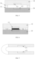
- FIG 1 is a first structural diagram of a pressure sensitive button according to an embodiment of this application.
- the pressure sensitive button in this embodiment of this application includes a first circuit board 10, a second circuit board 20, a first capacitor C1, a second capacitor C2, and a first connector 30.
- a first surface of the first circuit board 10 is disposed opposite to a second surface of the second circuit board 20.
- the first capacitor C1 is disposed on the first surface.
- the second capacitor C2 is disposed on the second surface.
- the first capacitor C1 is disposed opposite to the second capacitor C2.
- a first end of the first connector 30 is connected to the first surface.
- a second end of the first connector 30 is connected to the second surface.
- the first connector 30 is configured to limit the first surface to be parallel to the second surface.
- the first circuit board 10 may be a printed circuit board (Printed Circuit Board, PCB) or a flexible printed circuit (Flexible Printed Circuit, FPC); and the second circuit board 20 may be a printed circuit board or a flexible printed circuit. This is not specifically limited herein.
- first circuit board 10 is a flexible printed circuit
- a reinforcement plate is disposed on the side of the first circuit board 10 away from the second circuit board 20; and if the second circuit board 20 is a flexible printed circuit, a reinforcement plate is disposed on the side of the second circuit board 20 away from the first circuit board 10. Due to the additionally disposed reinforcement plates, strength of the circuit boards is improved. This facilitates overall assembly of the pressure sensitive button.
- the first surface of the first circuit board 10 is disposed opposite and parallel to the second surface of the second circuit board 20.
- the first capacitor C1 is disposed on the first surface.
- the second capacitor C2 is disposed on the second surface.
- the first capacitor C1 is disposed opposite to the second capacitor C2.
- the first circuit board 10 and the second circuit board 20 may be fastened to each other by welding with two solder balls.
- the size of the solder ball is related to the temperature of welding, the thickness of a steel mesh, the viscosity of solder paste, the speed of a scraper during welding, and the like.
- a relatively thick steel mesh needs to be used for printing with the solder paste. For example, a steel mesh whose thickness is 0.2 mm or 0.18 mm is used.
- the sizes of the two solder balls are usually inconsistent. If the sizes of the two solder balls are inconsistent, the first circuit board 10 and the second circuit board 20 are not parallel to each other. As a result, after the pressure sensitive button is pressed with force, variations of capacitances cannot be measured accurately, which easily causes an accidental touch. This reduces the reliability of the pressure sensitive button.
- the first connector 30 is disposed between the first circuit board 10 and the second circuit board 20. That the first connector 30 is configured to limit the first surface to be parallel to the second surface means that the first connector 30 is configured to limit the first circuit board 10 to be parallel to the second circuit board 20.
- first circuit board 10 being parallel to the second circuit board 20 means that the distance between the first circuit board 10 and the second circuit board 20 is within a preset range.
- the distance between the first circuit board 10 and the second circuit board 20 is greater than or equal to 50 ⁇ m and less than or equal to 150 ⁇ m.
- FIG 3 is a schematic diagram of a pressure sensitive button pressed with force according to an embodiment of this application.
- the distance between the first circuit board 10 and the second circuit board 20 is d 0 ; and after the pressure sensitive button is pressed with force, the distance between the first circuit board 10 and the second circuit board 20 is d F .
- the difference between d 0 and d F may be defined as ⁇ d.
- ⁇ d may also be understood as a variation of the distance between the first circuit board 10 and the second circuit board 20 after the pressure sensitive button is pressed with force.
- the pressure sensitive button in the embodiments of this application does not need to be disposed on a surface of an electronic device. This decreases an overall stacking thickness of the electronic device, so that the electronic device is lighter and thinner.
- the first end of the first connector 30 is fastened to the first circuit board 10 by bonding
- the second end of the first connector 30 is fastened to the second circuit board 20 by bonding
- the first circuit board 10 is electrically connected to the second circuit board 20 through the first connector 30.
- the first connector 30 is conductive adhesive.
- the first end of the first connector 30 is fastened to the first circuit board 10 by bonding according to a lamination process.
- the second end of the first connector 30 is fastened to the second circuit board 20 by bonding, so that the first circuit board 10 is parallel to the second circuit board 20.
- the first circuit board 10 and the second circuit board 20 may also be electrically connected to each other through the first connector 30.
- the thickness of the first connector 30 after lamination is less than the thickness of the first connector 30 before the lamination.
- the thickness of the first connector 30 after the lamination may be 40 ⁇ m. If the conventional thickness of the first connector 30 is 40 ⁇ m, the thickness of the first connector 30 after the lamination may be 25 ⁇ m.
- the first connector 30 is conductive adhesive, and the conductive adhesive is in a solidified state. It should be understood that in some embodiments, the first connector 30 may alternatively be made of another material that has an electricity conducting function. This is not specifically limited herein.
- the first connector 30 includes a metal reinforcement plate 31, a first conductive adhesive layer 32, and a second conductive adhesive layer 33; the first conductive adhesive layer 32 is disposed between the first circuit board 10 and the metal reinforcement plate 31; and the second conductive adhesive layer 33 is disposed between the second circuit board 20 and the metal reinforcement plate 31.
- the first connector 30 includes the metal reinforcement plate 31, the first conductive adhesive layer 32, and the second conductive adhesive layer 33.
- the metal reinforcement plate 31 is disposed between the first conductive adhesive layer 32 and the second conductive adhesive layer 33.
- the first conductive adhesive layer 32 is fastened to the first circuit board 10 by bonding.
- the second conductive adhesive layer 33 is fastened to the second circuit board 20 by bonding.
- the first conductive adhesive layer 32 and the second conductive adhesive layer 33 are made of conductive adhesive.
- the metal reinforcement plate 31 may be made of stainless steel or another metal. This is not specifically limited herein.
- disposing the metal reinforcement plate 31 between the first conductive adhesive layer 32 and the second conductive adhesive layer 33 not only limits the first circuit board 10 to be parallel to the second circuit board 20, but also can decrease usage of conductive adhesive, thereby decreasing the production cost of the pressure sensitive button.
- the first connector 30 includes at least one of a first pad 34 that is disposed in a first welding region of the first circuit board 10 and a second pad 35 that is disposed in a second welding region of the second circuit board 20; the first pad 34 protrudes from the first surface of the first circuit board 10; and the second pad 35 protrudes from the second surface of the second circuit board 20.
- the first connector 30 includes the first pad 34 and the second pad 35.
- the first pad 34 is disposed in the first welding region of the first circuit board 10.
- the second pad 35 is disposed in the second welding region of the second circuit board 20. Disposing of the first pad 34 and the second pad 35 decreases the distance between the first circuit board 10 and the second circuit board 20 in a welding region. Solder balls are welded between the first pad 34 and the second pad 35, so that the first circuit board 10 and the second circuit board 20 are parallel to each other.
- disposing of the first pad 34 and the second pad 35 decreases the distance between the first circuit board 10 and the second circuit board 20 in the welding region. For example, if both the first pad 34 and the second pad 35 are 25 ⁇ m high, the distance between the first circuit board 10 and the second circuit board 20 in the welding region may be decreased by 50 ⁇ m. In this case, a relatively thin steel mesh may be used for printing with solder paste to form solder balls whose sizes are consistent. This ensures that the two circuit boards are parallel to each other.
- the first connector 30 is the first pad 34; and the first pad 34 protrudes from the first surface of the first circuit board 10.
- the first connector 30 is the second pad 35; and the second pad 35 protrudes from the second surface of the second circuit board 20.
- the first connector 30 is the first pad 34, and the first pad 34 is fastened to the second welding region by welding;
- solder balls may be welded between the first pad 34 and the second welding region, so that first pad 34 is fastened to the second welding region by welding.
- the first circuit board 10 and the second circuit board 20 are electrically connected to each other by using the first pad 34 and the solder balls.
- solder balls may be welded between the second pad 35 and the first welding region, so that second pad 35 is fastened to the first welding region by welding.
- the first circuit board 10 and the second circuit board 20 are electrically connected to each other by using the second pad 35 and the solder balls.
- solder balls may be welded between the first pad 34 and the second pad 35, so that first pad 34 is fastened to the second pad 35 by welding.
- the first circuit board 10 and the second circuit board 20 are electrically connected to each other by using the first pad 34 and the second pad 35.
- the first connector 30 is a first elastic member 36; and the first circuit board 10 is fastened to the second circuit board 20 by welding.
- a first end of the first elastic member 36 is connected to the first capacitor C1; and a second end of the first elastic member 36 is connected to the second capacitor C2.
- the first connector 30 is a first elastic member 36.
- the first circuit board 10 is kept parallel to the second circuit board 20.
- the first elastic member 36 is made of a high temperature-resistant elastic material, for example, all-aromatic polyimide, a high temperature-resistant polyurethane elastomer, or another material.
- the first end of the first elastic member 36 is connected to the first capacitor C1; the second end of the first elastic member 36 is connected to the second capacitor; and the first circuit board 10 is fastened to the second circuit board 20 by welding.
- solder balls may be welded between the first circuit board 10 and the second circuit board 20 to fasten the first circuit board 10 and the second circuit board 20.
- the distance between the first circuit board 10 and the second circuit board 20 is the same as the thickness of the first elastic member 36.
- the first elastic member 36 is not disposed between the first capacitor C1 and the second capacitor C2. In this case, it may also be ensured that the first circuit board 10 and the second circuit board 20 are parallel to each other.
- the first circuit board 10 and the second circuit board 20 are a same circuit board and are flexible printed circuits.
- the circuit board may be bent to form two surfaces that are parallel to each other, as shown in FIG 7 which is a fifth structural diagram of a pressure sensitive button according to an embodiment of this application.
- the first capacitor C1 is disposed on one of the surfaces of the circuit board.
- the second capacitor C2 is disposed on the other surface of the circuit board.
- the first capacitor C1 is disposed opposite to the second capacitor C2.
- FIG 8 is a schematic diagram of a local structure of an electronic device according to an embodiment of this application.
- the electronic device includes a housing 40, a second connector 50, and the pressure sensitive button described above.
- the second connector 50 is disposed between the housing 40 and the pressure sensitive button.
- the second connector 50 is configured to limit the pressure sensitive button to be fastened to the housing 40.
- the electronic device includes the housing 40, the second connector 50, and the pressure sensitive button.
- the pressure sensitive button includes the first circuit board 10 and the second circuit board 20 that are parallel to each other.
- the first capacitor C1 is disposed on the first circuit board 10.
- the second capacitor C2 is disposed on the second circuit board 20.
- the distance between the first circuit board 10 and the second circuit board 20 is changed. Accordingly, a capacitance between the first capacitor C1 and the second capacitor C2 is also changed to respond to the press operation of the user based on a variation of the capacitance.
- a reinforcement plate may be disposed on the side of the first circuit board 10 away from the second circuit board 20.
- One end of the second connector 50 is connected to the housing 40, and the other end of the second connector 50 is connected to the reinforcement plate, so that the pressure sensitive button is fastened to the housing 40.
- the second connector 50 may be double-sided adhesive.
- the bonding force of double-sided adhesive is decreased in an environment having relatively high temperature or relatively high humidity. This may cause the pressure sensitive button to fall off from the housing 40.
- the pressure sensitive button may also fall off from the housing 40.
- the second connector 50 may be provided as a second elastic member.
- the second connector 50 is a second elastic member; a first end of the second elastic member is connected to the housing 40; and a second end of the second elastic member is connected to the pressure sensitive button.
- the second elastic member is a spring.
- the first end of the second elastic member is connected to the housing 40.
- the second end of the second elastic member is connected to the pressure sensitive button. Because the spring is insusceptible to temperature and humidity, the pressure sensitive button will not fall off from the housing 40 even in an environment having relatively high temperature and relatively high humidity.
- the second elastic member may also perform a buffering function to prevent the pressure sensitive button from falling off from the housing 40.
- the foregoing electronic device may be a computer (Computer), a mobile phone, a tablet personal computer (Tablet Personal Computer), a laptop computer (Laptop Computer), a personal digital assistant (personal digital assistant, PDA), a mobile Internet device (Mobile Internet Device, MID), a wearable device (Wearable Device), an e-book reader, a navigator, a digital camera, or the like.
- a computer Computer
- Tablet Personal Computer Tablet Personal Computer
- laptop computer laptop computer
- PDA personal digital assistant
- mobile Internet device Mobile Internet Device, MID
- Wearable Device wearable device
- e-book reader e-book reader
Landscapes
- Engineering & Computer Science (AREA)
- Microelectronics & Electronic Packaging (AREA)
- Coupling Device And Connection With Printed Circuit (AREA)
- Combinations Of Printed Boards (AREA)
- Push-Button Switches (AREA)
Abstract
Description
- This application claims priority to
Chinese Patent Application No. 202110771201.1, filed on July 8, 2021 - This application belongs to the field of electronic devices, and specifically relates to a pressure sensitive button and an electronic device.
- Currently, most electronic devices use press-type mechanical buttons. A user may press a mechanical button on an electronic device to implement a corresponding touch operation. However, the mechanical button is generally disposed on a surface of the electronic device. This increases an overall stacking thickness of the electronic device.
- Embodiments of this application aim to provide a pressure sensitive button and an electronic device, to resolve a technical problem that an existing mechanical button increases an overall stacking thickness.
- To resolve the technical problem, this application is implemented as follows:
- According to a first aspect, an embodiment of this application provides a pressure sensitive button, including a first circuit board, a second circuit board, a first capacitor, a second capacitor, and a first connector, where
- a first surface of the first circuit board is disposed opposite to a second surface of the second circuit board, the first capacitor is disposed on the first surface, the second capacitor is disposed on the second surface, the first capacitor is disposed opposite to the second capacitor, a first end of the first connector is connected to the first surface, and a second end of the first connector is connected to the second surface; and
- the first connector is configured to limit the first surface to be parallel to the second surface.
- According to a second aspect, an embodiment of this application provides an electronic device, including a housing, a second connector, and the pressure sensitive button according to the first aspect.
- According to the embodiments of this application, a pressure sensitive button includes a first circuit board, a second circuit board, a first capacitor, a second capacitor, and a first connector, where a first surface of the first circuit board is disposed opposite to a second surface of the second circuit board, the first capacitor is disposed on the first surface, the second capacitor is disposed on the second surface, the first capacitor is disposed opposite to the second capacitor, a first end of the first connector is connected to the first surface, a second end of the first connector is connected to the second surface, and the first connector is configured to limit the first surface to be parallel to the second surface. The pressure sensitive button in the embodiments of this application does not need to be disposed on a surface of an electronic device. This decreases an overall stacking thickness of the electronic device, so that the electronic device is lighter and thinner.
-
-
FIG 1 is a first structural diagram of a pressure sensitive button according to an embodiment of this application; -
FIG 2 is a structural diagram of a pressure sensitive button in the prior art; -
FIG 3 is a schematic diagram of a pressure sensitive button pressed with force according to an embodiment of this application; -
FIG 4 is a second structural diagram of a pressure sensitive button according to an embodiment of this application; -
FIG 5 is a third structural diagram of a pressure sensitive button according to an embodiment of this application; -
FIG 6 is a fourth structural diagram of a pressure sensitive button according to an embodiment of this application; -
FIG 7 is a fifth structural diagram of a pressure sensitive button according to an embodiment of this application; and -
FIG 8 is a schematic diagram of a local structure of an electronic device according to an embodiment of this application. - The following clearly and completely describes technical solutions in embodiments of this application with reference to accompanying drawings in the embodiments of this application. Apparently, the described embodiments are some but not all of the embodiments of this application. All other embodiments obtained by a person of ordinary skill in the art based on the embodiments of this application without creative efforts shall fall within the protection scope of this application.
- The terms "first", "second", and the like in this specification and the claims of this application are used to distinguish between similar objects instead of describing a specific order or sequence. It should be understood that the data used in such a way is interchangeable in proper circumstances so that the embodiments of this application can be implemented in an order other than the order illustrated or described herein. In addition, in this specification and the claims, "and/or" represents at least one of connected objects, and a character "/" generally represents an "or" relationship between associated objects.
- Refer to
FIG 1 which is a first structural diagram of a pressure sensitive button according to an embodiment of this application. As shown inFIG 1 , the pressure sensitive button in this embodiment of this application includes afirst circuit board 10, asecond circuit board 20, a first capacitor C1, a second capacitor C2, and afirst connector 30. - A first surface of the
first circuit board 10 is disposed opposite to a second surface of thesecond circuit board 20. The first capacitor C1 is disposed on the first surface. The second capacitor C2 is disposed on the second surface. The first capacitor C1 is disposed opposite to the second capacitor C2. A first end of thefirst connector 30 is connected to the first surface. A second end of thefirst connector 30 is connected to the second surface. - The
first connector 30 is configured to limit the first surface to be parallel to the second surface. - In this embodiment, the
first circuit board 10 may be a printed circuit board (Printed Circuit Board, PCB) or a flexible printed circuit (Flexible Printed Circuit, FPC); and thesecond circuit board 20 may be a printed circuit board or a flexible printed circuit. This is not specifically limited herein. - It should be understood that if the
first circuit board 10 is a flexible printed circuit, a reinforcement plate is disposed on the side of thefirst circuit board 10 away from thesecond circuit board 20; and if thesecond circuit board 20 is a flexible printed circuit, a reinforcement plate is disposed on the side of thesecond circuit board 20 away from thefirst circuit board 10. Due to the additionally disposed reinforcement plates, strength of the circuit boards is improved. This facilitates overall assembly of the pressure sensitive button. - As shown in
FIG 1 , the first surface of thefirst circuit board 10 is disposed opposite and parallel to the second surface of thesecond circuit board 20. The first capacitor C1 is disposed on the first surface. The second capacitor C2 is disposed on the second surface. The first capacitor C1 is disposed opposite to the second capacitor C2. In this way, after the pressure sensitive button is pressed with force, the distance between thefirst circuit board 10 and thesecond circuit board 20 is changed. Accordingly, capacitances of the first capacitor C1 and the second capacitor C2 are also changed to respond to a press operation of a user. - In a possible case, as shown in
FIG 2 , thefirst circuit board 10 and thesecond circuit board 20 may be fastened to each other by welding with two solder balls. However, the size of the solder ball is related to the temperature of welding, the thickness of a steel mesh, the viscosity of solder paste, the speed of a scraper during welding, and the like. In addition, if the distance between the two circuit boards is too large, a large quantity of solder paste needs to be used to form the solder balls. In this case, a relatively thick steel mesh needs to be used for printing with the solder paste. For example, a steel mesh whose thickness is 0.2 mm or 0.18 mm is used. Due to impacts of the foregoing factors, in an actual operation process, the sizes of the two solder balls are usually inconsistent. If the sizes of the two solder balls are inconsistent, thefirst circuit board 10 and thesecond circuit board 20 are not parallel to each other. As a result, after the pressure sensitive button is pressed with force, variations of capacitances cannot be measured accurately, which easily causes an accidental touch. This reduces the reliability of the pressure sensitive button. - To avoid the foregoing case, in this embodiment, the
first connector 30 is disposed between thefirst circuit board 10 and thesecond circuit board 20. That thefirst connector 30 is configured to limit the first surface to be parallel to the second surface means that thefirst connector 30 is configured to limit thefirst circuit board 10 to be parallel to thesecond circuit board 20. - It should be understood that the
first circuit board 10 being parallel to thesecond circuit board 20 means that the distance between thefirst circuit board 10 and thesecond circuit board 20 is within a preset range. Optionally, the distance between thefirst circuit board 10 and thesecond circuit board 20 is greater than or equal to 50 µm and less than or equal to 150 µm. - Further, refer to
FIG 3 which is a schematic diagram of a pressure sensitive button pressed with force according to an embodiment of this application. As shown inFIG 3 , before the pressure sensitive button is pressed with force, the distance between thefirst circuit board 10 and thesecond circuit board 20 is d0; and after the pressure sensitive button is pressed with force, the distance between thefirst circuit board 10 and thesecond circuit board 20 is dF. Herein, the difference between d0 and dF may be defined as Δd. Δd may also be understood as a variation of the distance between thefirst circuit board 10 and thesecond circuit board 20 after the pressure sensitive button is pressed with force. Therefore, a variation of a capacitance after the pressure sensitive button is pressed with force may be represented by using the following formula:
ΔC is a variation of a capacitance; εr and ε0 are preset dielectric constants; S is an area by which thefirst circuit board 10 and thesecond circuit board 20 are disposed opposite to each other; d0 is a distance between thefirst circuit board 10 and thesecond circuit board 20; and Δd is a variation of the distance between thefirst circuit board 10 and thesecond circuit board 20 after the pressure sensitive button is pressed with force. - In this embodiment of this application, after a user presses the pressure sensitive button with force, the distance between two parallel circuit boards is changed. Therefore, capacitances of two capacitors that are disposed on the two parallel circuit boards and opposite to each other are changed to respond to the press operation of the user. The pressure sensitive button in the embodiments of this application does not need to be disposed on a surface of an electronic device. This decreases an overall stacking thickness of the electronic device, so that the electronic device is lighter and thinner.
- Optionally, the first end of the
first connector 30 is fastened to thefirst circuit board 10 by bonding, the second end of thefirst connector 30 is fastened to thesecond circuit board 20 by bonding, and thefirst circuit board 10 is electrically connected to thesecond circuit board 20 through thefirst connector 30. - Optionally, the
first connector 30 is conductive adhesive. - In this embodiment, the first end of the
first connector 30 is fastened to thefirst circuit board 10 by bonding according to a lamination process. The second end of thefirst connector 30 is fastened to thesecond circuit board 20 by bonding, so that thefirst circuit board 10 is parallel to thesecond circuit board 20. Moreover, thefirst circuit board 10 and thesecond circuit board 20 may also be electrically connected to each other through thefirst connector 30. - It should be understood that the thickness of the
first connector 30 after lamination is less than the thickness of thefirst connector 30 before the lamination. For example, if the conventional thickness of thefirst connector 30 is 60 µm, that is, the thickness of thefirst connector 30 before the lamination is 60 µm, the thickness of thefirst connector 30 after the lamination may be 40 µm. If the conventional thickness of thefirst connector 30 is 40 µm, the thickness of thefirst connector 30 after the lamination may be 25 µm. - In an optional implementation, the
first connector 30 is conductive adhesive, and the conductive adhesive is in a solidified state. It should be understood that in some embodiments, thefirst connector 30 may alternatively be made of another material that has an electricity conducting function. This is not specifically limited herein. - Optionally, the
first connector 30 includes ametal reinforcement plate 31, a first conductiveadhesive layer 32, and a second conductiveadhesive layer 33; the first conductiveadhesive layer 32 is disposed between thefirst circuit board 10 and themetal reinforcement plate 31; and the second conductiveadhesive layer 33 is disposed between thesecond circuit board 20 and themetal reinforcement plate 31. - Refer to
FIG 4 which is a second structural diagram of a pressure sensitive button according to an embodiment of this application. As shown inFIG 4 , thefirst connector 30 includes themetal reinforcement plate 31, the first conductiveadhesive layer 32, and the second conductiveadhesive layer 33. Themetal reinforcement plate 31 is disposed between the first conductiveadhesive layer 32 and the second conductiveadhesive layer 33. The first conductiveadhesive layer 32 is fastened to thefirst circuit board 10 by bonding. The second conductiveadhesive layer 33 is fastened to thesecond circuit board 20 by bonding. The first conductiveadhesive layer 32 and the second conductiveadhesive layer 33 are made of conductive adhesive. Themetal reinforcement plate 31 may be made of stainless steel or another metal. This is not specifically limited herein. - In this embodiment, disposing the
metal reinforcement plate 31 between the first conductiveadhesive layer 32 and the second conductiveadhesive layer 33 not only limits thefirst circuit board 10 to be parallel to thesecond circuit board 20, but also can decrease usage of conductive adhesive, thereby decreasing the production cost of the pressure sensitive button. - Optionally, the
first connector 30 includes at least one of afirst pad 34 that is disposed in a first welding region of thefirst circuit board 10 and asecond pad 35 that is disposed in a second welding region of thesecond circuit board 20; thefirst pad 34 protrudes from the first surface of thefirst circuit board 10; and thesecond pad 35 protrudes from the second surface of thesecond circuit board 20. - Refer to
FIG 5 which is a third structural diagram of a pressure sensitive button according to an embodiment of this application. As shown inFIG 5 , thefirst connector 30 includes thefirst pad 34 and thesecond pad 35. Thefirst pad 34 is disposed in the first welding region of thefirst circuit board 10. Thesecond pad 35 is disposed in the second welding region of thesecond circuit board 20. Disposing of thefirst pad 34 and thesecond pad 35 decreases the distance between thefirst circuit board 10 and thesecond circuit board 20 in a welding region. Solder balls are welded between thefirst pad 34 and thesecond pad 35, so that thefirst circuit board 10 and thesecond circuit board 20 are parallel to each other. - As described above, when the distance between the two circuit boards is too large, a relatively thick steel mesh needs to be used for printing with solder paste to form solder balls. This easily causes that the sizes of the solder balls are inconsistent. As a result, the two circuit boards are not parallel to each other.
- In this embodiment, disposing of the
first pad 34 and thesecond pad 35 decreases the distance between thefirst circuit board 10 and thesecond circuit board 20 in the welding region. For example, if both thefirst pad 34 and thesecond pad 35 are 25 µm high, the distance between thefirst circuit board 10 and thesecond circuit board 20 in the welding region may be decreased by 50 µm. In this case, a relatively thin steel mesh may be used for printing with solder paste to form solder balls whose sizes are consistent. This ensures that the two circuit boards are parallel to each other. - In an optional implementation, the
first connector 30 is thefirst pad 34; and thefirst pad 34 protrudes from the first surface of thefirst circuit board 10. - In another optional implementation, the
first connector 30 is thesecond pad 35; and thesecond pad 35 protrudes from the second surface of thesecond circuit board 20. - Optionally, the
first connector 30 is thefirst pad 34, and thefirst pad 34 is fastened to the second welding region by welding; - the
first connector 30 is thesecond pad 35, and thesecond pad 35 is fastened to the first welding region by welding; or - the
first connector 30 includes thefirst pad 34 and thesecond pad 35, and thefirst pad 34 is fastened to thesecond pad 35 by welding. - In this embodiment, in a case that the
first connector 30 is thefirst pad 34, solder balls may be welded between thefirst pad 34 and the second welding region, so thatfirst pad 34 is fastened to the second welding region by welding. Thefirst circuit board 10 and thesecond circuit board 20 are electrically connected to each other by using thefirst pad 34 and the solder balls. - In a case that the
first connector 30 is thesecond pad 35, solder balls may be welded between thesecond pad 35 and the first welding region, so thatsecond pad 35 is fastened to the first welding region by welding. Thefirst circuit board 10 and thesecond circuit board 20 are electrically connected to each other by using thesecond pad 35 and the solder balls. - In a case that the
first connector 30 includes thefirst pad 34 and thesecond pad 35, solder balls may be welded between thefirst pad 34 and thesecond pad 35, so thatfirst pad 34 is fastened to thesecond pad 35 by welding. Thefirst circuit board 10 and thesecond circuit board 20 are electrically connected to each other by using thefirst pad 34 and thesecond pad 35. - Optionally, the
first connector 30 is a firstelastic member 36; and thefirst circuit board 10 is fastened to thesecond circuit board 20 by welding. - Optionally, a first end of the first
elastic member 36 is connected to the first capacitor C1; and a second end of the firstelastic member 36 is connected to the second capacitor C2. - Refer to
FIG 6 . As shown inFIG 6 , in this embodiment, thefirst connector 30 is a firstelastic member 36. By disposing the firstelastic member 36, thefirst circuit board 10 is kept parallel to thesecond circuit board 20. To prevent the firstelastic member 36 from deforming in a welding process, the firstelastic member 36 is made of a high temperature-resistant elastic material, for example, all-aromatic polyimide, a high temperature-resistant polyurethane elastomer, or another material. - The first end of the first
elastic member 36 is connected to the first capacitor C1; the second end of the firstelastic member 36 is connected to the second capacitor; and thefirst circuit board 10 is fastened to thesecond circuit board 20 by welding. As shown inFIG 6 , solder balls may be welded between thefirst circuit board 10 and thesecond circuit board 20 to fasten thefirst circuit board 10 and thesecond circuit board 20. As shown inFIG 6 , the distance between thefirst circuit board 10 and thesecond circuit board 20 is the same as the thickness of the firstelastic member 36. - It should be understood that in some embodiments, the first
elastic member 36 is not disposed between the first capacitor C1 and the second capacitor C2. In this case, it may also be ensured that thefirst circuit board 10 and thesecond circuit board 20 are parallel to each other. - In a possible case, the
first circuit board 10 and thesecond circuit board 20 are a same circuit board and are flexible printed circuits. In this case, the circuit board may be bent to form two surfaces that are parallel to each other, as shown inFIG 7 which is a fifth structural diagram of a pressure sensitive button according to an embodiment of this application. - In the circuit board shown in
FIG 7 , two surfaces of the circuit board are parallel to each other. The first capacitor C1 is disposed on one of the surfaces of the circuit board. The second capacitor C2 is disposed on the other surface of the circuit board. The first capacitor C1 is disposed opposite to the second capacitor C2. - Refer to
FIG 8 which is a schematic diagram of a local structure of an electronic device according to an embodiment of this application. In this embodiment of this application, an electronic device is further provided. The electronic device includes ahousing 40, asecond connector 50, and the pressure sensitive button described above. Thesecond connector 50 is disposed between thehousing 40 and the pressure sensitive button. Thesecond connector 50 is configured to limit the pressure sensitive button to be fastened to thehousing 40. - As shown in
FIG 8 , the electronic device includes thehousing 40, thesecond connector 50, and the pressure sensitive button. The pressure sensitive button includes thefirst circuit board 10 and thesecond circuit board 20 that are parallel to each other. The first capacitor C1 is disposed on thefirst circuit board 10. The second capacitor C2 is disposed on thesecond circuit board 20. - When a user presses the pressure sensitive button on the electronic device, the distance between the
first circuit board 10 and thesecond circuit board 20 is changed. Accordingly, a capacitance between the first capacitor C1 and the second capacitor C2 is also changed to respond to the press operation of the user based on a variation of the capacitance. - As described above, if the
first circuit board 10 in the pressure sensitive button is a flexible printed circuit, a reinforcement plate may be disposed on the side of thefirst circuit board 10 away from thesecond circuit board 20. One end of thesecond connector 50 is connected to thehousing 40, and the other end of thesecond connector 50 is connected to the reinforcement plate, so that the pressure sensitive button is fastened to thehousing 40. - It should be understood that for a specific implementation of the pressure sensitive button, refer to the foregoing descriptions, and a same technical effect can be achieved. To avoid repetition, details are not described again.
- Optionally, the
second connector 50 may be double-sided adhesive. However, the bonding force of double-sided adhesive is decreased in an environment having relatively high temperature or relatively high humidity. This may cause the pressure sensitive button to fall off from thehousing 40. In addition, in a case that the electronic device suffers an external force, the pressure sensitive button may also fall off from thehousing 40. - To resolve the foregoing possible technical problem, the
second connector 50 may be provided as a second elastic member. - Optionally, the
second connector 50 is a second elastic member; a first end of the second elastic member is connected to thehousing 40; and a second end of the second elastic member is connected to the pressure sensitive button. - In an optional implementation, the second elastic member is a spring. The first end of the second elastic member is connected to the
housing 40. The second end of the second elastic member is connected to the pressure sensitive button. Because the spring is insusceptible to temperature and humidity, the pressure sensitive button will not fall off from thehousing 40 even in an environment having relatively high temperature and relatively high humidity. When the electronic device suffers an external force, the second elastic member may also perform a buffering function to prevent the pressure sensitive button from falling off from thehousing 40. - In this embodiment of the present invention, the foregoing electronic device may be a computer (Computer), a mobile phone, a tablet personal computer (Tablet Personal Computer), a laptop computer (Laptop Computer), a personal digital assistant (personal digital assistant, PDA), a mobile Internet device (Mobile Internet Device, MID), a wearable device (Wearable Device), an e-book reader, a navigator, a digital camera, or the like.
- The embodiments of this application are described above with reference to the accompanying drawings. However, this application is not limited to the foregoing specific implementations. The foregoing specific implementations are merely illustrative instead of restrictive. Under the enlightenment of this application, a person of ordinary skill in the art may make many forms without departing from the essence of this application and the protection scope of the claims, all of which fall within the protection of this application.
Claims (10)
- A pressure sensitive button, comprising a first circuit board, a second circuit board, a first capacitor, a second capacitor, and a first connector, whereina first surface of the first circuit board is disposed opposite to a second surface of the second circuit board, the first capacitor is disposed on the first surface, the second capacitor is disposed on the second surface, the first capacitor is disposed opposite to the second capacitor, a first end of the first connector is connected to the first surface, and a second end of the first connector is connected to the second surface; andthe first connector is configured to limit the first surface to be parallel to the second surface.
- The pressure sensitive button according to claim 1, wherein the first end of the first connector is fastened to the first circuit board by bonding, the second end of the first connector is fastened to the second circuit board by bonding, and the first circuit board is electrically connected to the second circuit board through the first connector.
- The pressure sensitive button according to claim 2, wherein the first connector is conductive adhesive.
- The pressure sensitive button according to claim 1, wherein the first connector comprises a metal reinforcement plate, a first conductive adhesive layer, and a second conductive adhesive layer, the first conductive adhesive layer is disposed between the first circuit board and the metal reinforcement plate, and the second conductive adhesive layer is disposed between the second circuit board and the metal reinforcement plate.
- The pressure sensitive button according to claim 1, wherein the first connector comprises at least one of a first pad that is disposed in a first welding region of the first circuit board and a second pad that is disposed in a second welding region of the second circuit board, the first pad protrudes from the first surface of the first circuit board, and the second pad protrudes from the second surface of the second circuit board.
- The pressure sensitive button according to claim 5, wherein the first connector is the first pad, and the first pad is fastened to the second welding region by welding;the first connector is the second pad, and the second pad is fastened to the first welding region by welding; orthe first connector comprises the first pad and the second pad, and the first pad is fastened to the second pad by welding.
- The pressure sensitive button according to claim 1, wherein the first connector is a first elastic member, and the first circuit board is fastened to the second circuit board by welding.
- The pressure sensitive button according to claim 7, wherein a first end of the first elastic member is connected to the first capacitor, and a second end of the first elastic member is connected to the second capacitor.
- An electronic device, wherein the electronic device comprises a housing, a second connector, and the pressure sensitive button according to any one of claims 1 to 8, the second connector is disposed between the housing and the pressure sensitive button, and the second connector is configured to limit the pressure sensitive button to be fastened to the housing.
- The electronic device according to claim 9, wherein the second connector is a second elastic member, a first end of the second elastic member is connected to the housing, and a second end of the second elastic member is connected to the pressure sensitive button.
Applications Claiming Priority (2)
| Application Number | Priority Date | Filing Date | Title |
|---|---|---|---|
| CN202110771201.1A CN113346890B (en) | 2021-07-08 | 2021-07-08 | Pressure-sensitive key and electronic equipment |
| PCT/CN2022/103334 WO2023280072A1 (en) | 2021-07-08 | 2022-07-01 | Pressure-sensitive key and electronic device |
Publications (2)
| Publication Number | Publication Date |
|---|---|
| EP4369607A1 true EP4369607A1 (en) | 2024-05-15 |
| EP4369607A4 EP4369607A4 (en) | 2024-11-06 |
Family
ID=77483103
Family Applications (1)
| Application Number | Title | Priority Date | Filing Date |
|---|---|---|---|
| EP22836823.9A Pending EP4369607A4 (en) | 2021-07-08 | 2022-07-01 | Pressure-sensitive key and electronic device |
Country Status (4)
| Country | Link |
|---|---|
| US (1) | US20240146303A1 (en) |
| EP (1) | EP4369607A4 (en) |
| CN (1) | CN113346890B (en) |
| WO (1) | WO2023280072A1 (en) |
Families Citing this family (2)
| Publication number | Priority date | Publication date | Assignee | Title |
|---|---|---|---|---|
| CN113346890B (en) * | 2021-07-08 | 2023-08-08 | 维沃移动通信有限公司 | Pressure-sensitive key and electronic equipment |
| CN114863826B (en) * | 2022-04-12 | 2023-06-27 | 武汉华星光电半导体显示技术有限公司 | Display screen and manufacturing method thereof |
Family Cites Families (17)
| Publication number | Priority date | Publication date | Assignee | Title |
|---|---|---|---|---|
| IT1183977B (en) * | 1985-11-27 | 1987-10-22 | Olivetti & Co Spa | MULTI-LAYER CAPACITIVE MEMBRANE FOR KEYBOARDS OF OFFICE MACHINES AND DATA PROCESSING EQUIPMENT |
| US20130018489A1 (en) * | 2011-07-14 | 2013-01-17 | Grunthaner Martin Paul | Combined force and proximity sensing |
| JP6237641B2 (en) * | 2012-11-08 | 2017-11-29 | 味の素株式会社 | Membrane switch and article using the same |
| US20160062500A1 (en) * | 2014-08-28 | 2016-03-03 | Apple Inc. | Force Sensor with Capacitive Gap Sensing |
| CN204808299U (en) * | 2015-07-29 | 2015-11-25 | 维沃移动通信有限公司 | Capacitive touch panel |
| US9870033B1 (en) * | 2016-08-30 | 2018-01-16 | Apple Inc. | Sensor assemblies for electronic devices |
| CN108256388A (en) * | 2016-12-28 | 2018-07-06 | 南昌欧菲生物识别技术有限公司 | Fingerprint recognition button and electronic device |
| CN206282307U (en) * | 2016-12-28 | 2017-06-27 | 南昌欧菲生物识别技术有限公司 | Fingerprint recognition button and electronic installation |
| WO2018227492A1 (en) * | 2017-06-15 | 2018-12-20 | 深圳市汇顶科技股份有限公司 | Button device for use in electronic equipment and electronic equipment |
| CN108346537B (en) * | 2018-02-06 | 2020-02-18 | 维沃移动通信有限公司 | A key structure and terminal |
| WO2020004651A1 (en) * | 2018-06-28 | 2020-01-02 | ソニー株式会社 | Sensor, input device, and electronic apparatus |
| CN210518263U (en) * | 2019-09-11 | 2020-05-12 | 佛吉亚(中国)投资有限公司 | Capacitance voltage detection mechanism and automobile including the same |
| DE102019006628A1 (en) * | 2019-09-20 | 2021-03-25 | Diehl Ako Stiftung & Co. Kg | Control device |
| CN111930274B (en) * | 2020-08-10 | 2022-05-31 | Oppo(重庆)智能科技有限公司 | Virtual key, electronic equipment and touch operation detection method |
| CN213210864U (en) * | 2020-10-22 | 2021-05-14 | 深圳瑞湖科技有限公司 | Touch module and electronic equipment |
| EP4068800A4 (en) * | 2021-02-09 | 2022-10-05 | Shenzhen Goodix Technology Co., Ltd. | Pressure detection module and electronic device |
| CN113346890B (en) * | 2021-07-08 | 2023-08-08 | 维沃移动通信有限公司 | Pressure-sensitive key and electronic equipment |
-
2021
- 2021-07-08 CN CN202110771201.1A patent/CN113346890B/en active Active
-
2022
- 2022-07-01 WO PCT/CN2022/103334 patent/WO2023280072A1/en not_active Ceased
- 2022-07-01 EP EP22836823.9A patent/EP4369607A4/en active Pending
-
2024
- 2024-01-08 US US18/406,608 patent/US20240146303A1/en active Pending
Also Published As
| Publication number | Publication date |
|---|---|
| WO2023280072A1 (en) | 2023-01-12 |
| CN113346890A (en) | 2021-09-03 |
| US20240146303A1 (en) | 2024-05-02 |
| EP4369607A4 (en) | 2024-11-06 |
| CN113346890B (en) | 2023-08-08 |
Similar Documents
| Publication | Publication Date | Title |
|---|---|---|
| US20240146303A1 (en) | Pressure sensitive button and electronic device | |
| US8913031B2 (en) | Sensor apparatus and electronic apparatus | |
| JP2011086191A (en) | Electronic apparatus | |
| US11829567B2 (en) | Touch pad, force touch apparatus, and electronic device | |
| US20230375419A1 (en) | Device for detecting user input with force sensor in stem thereof | |
| CN216118567U (en) | Touch pad assembly and electronic equipment | |
| CN206282307U (en) | Fingerprint recognition button and electronic installation | |
| CN214702567U (en) | Pressure sensor and electronic device | |
| CN114981761A (en) | Haptic effect device | |
| US8857276B2 (en) | Pressure detection unit | |
| US11202379B2 (en) | Electronic apparatus | |
| US11481080B2 (en) | Sensor device, input device, and electronic apparatus | |
| EP4016258B1 (en) | Display apparatus and terminal | |
| US6479775B2 (en) | Flat input device having push switches | |
| CN215954276U (en) | Touch pad and electronic equipment | |
| CN108256388A (en) | Fingerprint recognition button and electronic device | |
| CN113778245B (en) | Touch pad and electronic equipment | |
| KR101095180B1 (en) | Input device | |
| CN107077017B (en) | a terminal | |
| CN108256395A (en) | Fingerprint recognition button and electronic device | |
| US20160179202A1 (en) | Touch device and electronic equipment using the same | |
| US10831324B2 (en) | Touch panel and fabrication method thereof, touch display screen and fabrication method thereof | |
| CN210954807U (en) | Side button device of sensor module and equipment | |
| CN215954288U (en) | Connecting soft board, sensor module, touch device and electronic equipment | |
| CN218825380U (en) | Ultrathin touch control panel module |
Legal Events
| Date | Code | Title | Description |
|---|---|---|---|
| STAA | Information on the status of an ep patent application or granted ep patent |
Free format text: STATUS: THE INTERNATIONAL PUBLICATION HAS BEEN MADE |
|
| PUAI | Public reference made under article 153(3) epc to a published international application that has entered the european phase |
Free format text: ORIGINAL CODE: 0009012 |
|
| STAA | Information on the status of an ep patent application or granted ep patent |
Free format text: STATUS: REQUEST FOR EXAMINATION WAS MADE |
|
| 17P | Request for examination filed |
Effective date: 20240201 |
|
| AK | Designated contracting states |
Kind code of ref document: A1 Designated state(s): AL AT BE BG CH CY CZ DE DK EE ES FI FR GB GR HR HU IE IS IT LI LT LU LV MC MK MT NL NO PL PT RO RS SE SI SK SM TR |
|
| DAV | Request for validation of the european patent (deleted) | ||
| DAX | Request for extension of the european patent (deleted) | ||
| A4 | Supplementary search report drawn up and despatched |
Effective date: 20241007 |
|
| RIC1 | Information provided on ipc code assigned before grant |
Ipc: H05K 1/18 20060101ALI20240930BHEP Ipc: H05K 1/11 20060101ALI20240930BHEP Ipc: H03K 17/96 20060101ALI20240930BHEP Ipc: H03K 17/975 20060101AFI20240930BHEP |