EP4369423A1 - Method for activating absorption layer of thin-film solar cell - Google Patents
Method for activating absorption layer of thin-film solar cell Download PDFInfo
- Publication number
- EP4369423A1 EP4369423A1 EP22897093.5A EP22897093A EP4369423A1 EP 4369423 A1 EP4369423 A1 EP 4369423A1 EP 22897093 A EP22897093 A EP 22897093A EP 4369423 A1 EP4369423 A1 EP 4369423A1
- Authority
- EP
- European Patent Office
- Prior art keywords
- solar cell
- polyvinylchloride
- film
- absorber layer
- cdse
- Prior art date
- Legal status (The legal status is an assumption and is not a legal conclusion. Google has not performed a legal analysis and makes no representation as to the accuracy of the status listed.)
- Granted
Links
Images

Classifications
-
- H—ELECTRICITY
- H10—SEMICONDUCTOR DEVICES; ELECTRIC SOLID-STATE DEVICES NOT OTHERWISE PROVIDED FOR
- H10F—INORGANIC SEMICONDUCTOR DEVICES SENSITIVE TO INFRARED RADIATION, LIGHT, ELECTROMAGNETIC RADIATION OF SHORTER WAVELENGTH OR CORPUSCULAR RADIATION
- H10F71/00—Manufacture or treatment of devices covered by this subclass
-
- H—ELECTRICITY
- H10—SEMICONDUCTOR DEVICES; ELECTRIC SOLID-STATE DEVICES NOT OTHERWISE PROVIDED FOR
- H10F—INORGANIC SEMICONDUCTOR DEVICES SENSITIVE TO INFRARED RADIATION, LIGHT, ELECTROMAGNETIC RADIATION OF SHORTER WAVELENGTH OR CORPUSCULAR RADIATION
- H10F10/00—Individual photovoltaic cells, e.g. solar cells
- H10F10/10—Individual photovoltaic cells, e.g. solar cells having potential barriers
- H10F10/16—Photovoltaic cells having only PN heterojunction potential barriers
- H10F10/162—Photovoltaic cells having only PN heterojunction potential barriers comprising only Group II-VI materials, e.g. CdS/CdTe photovoltaic cells
-
- H—ELECTRICITY
- H10—SEMICONDUCTOR DEVICES; ELECTRIC SOLID-STATE DEVICES NOT OTHERWISE PROVIDED FOR
- H10F—INORGANIC SEMICONDUCTOR DEVICES SENSITIVE TO INFRARED RADIATION, LIGHT, ELECTROMAGNETIC RADIATION OF SHORTER WAVELENGTH OR CORPUSCULAR RADIATION
- H10F71/00—Manufacture or treatment of devices covered by this subclass
- H10F71/125—The active layers comprising only Group II-VI materials, e.g. CdS, ZnS or CdTe
-
- H—ELECTRICITY
- H10—SEMICONDUCTOR DEVICES; ELECTRIC SOLID-STATE DEVICES NOT OTHERWISE PROVIDED FOR
- H10F—INORGANIC SEMICONDUCTOR DEVICES SENSITIVE TO INFRARED RADIATION, LIGHT, ELECTROMAGNETIC RADIATION OF SHORTER WAVELENGTH OR CORPUSCULAR RADIATION
- H10F71/00—Manufacture or treatment of devices covered by this subclass
- H10F71/128—Annealing
-
- Y—GENERAL TAGGING OF NEW TECHNOLOGICAL DEVELOPMENTS; GENERAL TAGGING OF CROSS-SECTIONAL TECHNOLOGIES SPANNING OVER SEVERAL SECTIONS OF THE IPC; TECHNICAL SUBJECTS COVERED BY FORMER USPC CROSS-REFERENCE ART COLLECTIONS [XRACs] AND DIGESTS
- Y02—TECHNOLOGIES OR APPLICATIONS FOR MITIGATION OR ADAPTATION AGAINST CLIMATE CHANGE
- Y02E—REDUCTION OF GREENHOUSE GAS [GHG] EMISSIONS, RELATED TO ENERGY GENERATION, TRANSMISSION OR DISTRIBUTION
- Y02E10/00—Energy generation through renewable energy sources
- Y02E10/50—Photovoltaic [PV] energy
- Y02E10/543—Solar cells from Group II-VI materials
Definitions
- the present invention refers to a method of activating an absorber layer of a CdTe or CdSeTe thin-film solar cell without the use of CdCl 2 .
- producing superstrate configuration thin-film solar cells having an absorber layer comprising CdSe x Te 1-x (0 ⁇ x ⁇ 4 ⁇ m) involves applying a transparent front contact layer (TCO, i.e. transparent conductive oxide) onto a substrate (preferably glass).
- TCO transparent front contact layer
- the front contact layer may also be a layer stack consisting of several different layers.
- a layer of pure or modified CdS (cadmium sulfide) may be deposited.
- Modified CdS cadmium sulfide
- this CdS layer may also be omitted.
- an absorber layer of CdTe (cadmium telluride) or CdSe x Te 1-x (cadmium selenide telluride) is applied.
- the absorber layer in turn the back contact layer, or back layer sequence, is deposited.
- a CdCl 2 layer is applied to the absorber layer using methods according to the state of the art, e.g. wet-chemical methods, CVD (chemical vapour deposition) or PVD (physical vapour deposition).
- CVD chemical vapour deposition
- PVD physical vapour deposition
- the CdCl 2 is left to react with the absorber layer at a raised temperature, usually about 380°C to 430°C. Reaction time is about 15 minutes to 45 minutes.
- the CdClz acts as fluxing agent and supports a recrystallisation of the CdTe or CdSe x Te 1-x layer.
- CdCl 2 is an easily water-soluble, toxic chemical and highly hazardous for the environment. It is proven to have carcinogenic and mutagenic properties and to be toxic for reproduction. These properties require special care in handling when processing the CdCb in the production process. Furthermore, the generated contaminated waste water requires costly cleaning or waste disposal.
- hypochlorites of sodium, calcium or other alkaline or earth alkaline metals has been investigated in WO 2018/119679 A1 , wherein calcium hypochlorite (Ca(OCl) 2 ) has proven suitable.
- WO 2011/045728 A1 describes a method, wherein the absorber layer is treated with a mixture formed by a fluorine-free chlorinated hydrocarbon and by a chlorine-free fluorinated hydrocarbon.
- EP 1176644 A1 discloses a method using a gaseous mixture of hydrogen chloride, nitrogen and oxygen for activation.
- the object of the present invention consists in providing a further alternative method in which the CdCl 2 is replaced with a safer, and easier to handle substance. Furthermore, the overall method of producing a CdTe or CdSeTe thin-film solar cell should be maintained.
- the method according to the present invention comprises the steps of providing a semi-finished thin-film solar cell, forming a polyvinylchloride film, and performing a heat treatment.
- the semi-finished solar cell comprises an absorber layer comprising CdSe x Te 1-x , wherein 0 ⁇ x ⁇ 0.99, and the absorber layer may also be a layer stack comprising different material layers.
- the layer stack may - among other materials - comprise at least two layers selected from CdS, CdTe, ZnTe, CdSe. This is beneficial, as during activation, these stacked layers may intermix, leading to the formation of an absorber layer comprising CdSe x Te 1-x or the recrystallization of layers in different alloying states and mixing ratios.
- the semi-finished solar cell can therefore also comprise an absorber layer comprising CdSe, CdS or CdTe.
- the absorber layer is adjacent to a surface of the semi-finished thin-film solar cell, i.e. a surface of the absorber layer lies open and can be treated.
- the polyvinylchloride film is formed on this surface of the absorber layer.
- the heat treatment is performed when the polyvinylchloride film is formed on the absorber layer, wherein the temperature is in the range of 300°C to 500°C. Due to the temperature treatment, the polyvinylchloride film decomposes and the released hydrogen chloride (H + Cl - ) may enter the absorber layer via the surface and/or the grain boundaries and initiate the activation process.
- the heat treatment step may be performed at least at 300°C in order to fully decompose the polyvinylchloride film in an acceptable period of time. Furthermore, recrystallization processes within the absorber layer, which are part of the activation process, perform better at higher temperatures.
- the temperature may not rise above 500°C during heat treatment in order to avoid negative effects on other films already present in the semi-finished thin-film solar cell, e.g. transparent conductive oxides or a glass substrate.
- the temperature is in the range between 380°C and 450°C during heat treatment.
- the heat treatment may be performed for a time in the range of 5 minutes to 30 minutes.
- polyvinylchloride is less toxic and hazardous for the environment as CDCl 2 , safety requirements are less. Furthermore, products resulting from its decomposition may be treated with normal filter units already present in the process apparatuses used for fabricating CdSe x Te 1-x thin-film solar cells.
- the polyvinylchloride film is formed by applying a solid sheet of polyvinylchloride on the surface of the absorber layer.
- the sheet of polyvinylchloride may be provided from a roll and applied to the surface of the absorber layer by a roller.
- the sheet of polyvinylchloride may have a thickness in the range of 10 ⁇ m to 500 ⁇ m.
- the polyvinylchloride film is formed by applying a solvent in which the polyvinylchloride is dissolved, followed by drying of the film.
- the solvent may be an organic solvent, for instance tetrahydrofuran or dimethylformamide, or any other suitable solvent.
- the solvent may be applied using a roller coater, a spin coater, a scraper, or a spray coater. Drying may be performed at elevated temperatures, for instance 100°C, or at room temperature (between 18°C and 30°C) and results in transforming the liquid or pasty solvent film into a solid film or essentially solid film of polyvinylchloride by evaporation or sublimation of the solvent part.
- the temperature during drying may be below 200°C in order to prevent decomposition of the polyvinylchloride at this process stage.
- the surface of the absorber layer may be cleaned before forming the polyvinylchloride film on it.
- Cleaning agents known from the prior art e.g. isopropanol, or plasma cleaning processes can be used.
- the method further comprises a cleaning step performed after the heat treatment in order to remove organic residues resulting from the decomposed polyvinylchloride film.
- a cleaning step performed after the heat treatment in order to remove organic residues resulting from the decomposed polyvinylchloride film.
- At least one of the group comprising an aqueous inorganic acid, an organic complexing agent, an organic complexing acid, a mechanical cleaning device, a water jet or ultra sound may be used for cleaning the surface of the activated absorber layer.
- An aqueous inorganic acid may be, for instance, hydrochloric acid, nitric acid, phosphoric acid, hydroiodic acid or a mixture of some or all of these acids.
- An organic complexing agent may be, for instance, ethylenediamine or ethylenediaminetetraacetate (EDTA).
- An organic complexing acid may be, for instance, citric acid or tartaric acid.
- a mechanical cleaning device may comprise, for instance, soft brushes.
- the semi-finished thin-film solar cell may be treated further in order to fabricate a finished thin-film solar cell.
- Structuring processes, doping processes, temperature treatment processes and processes for forming a back contact layer (or back contact layer stack) may be performed. These processes are known to a person skilled in the art.
- FIGS 1 to 5 schematically show the sequence of process steps, including the activation step according to the invention using polyvinylchloride.
Landscapes
- Photovoltaic Devices (AREA)
- Life Sciences & Earth Sciences (AREA)
- Engineering & Computer Science (AREA)
- Sustainable Development (AREA)
- Sustainable Energy (AREA)
Abstract
Description
- The present invention refers to a method of activating an absorber layer of a CdTe or CdSeTe thin-film solar cell without the use of CdCl2.
- According to the state of the art, producing superstrate configuration thin-film solar cells having an absorber layer comprising CdSexTe1-x (0 ≤ x ≤ 4 µm) involves applying a transparent front contact layer (TCO, i.e. transparent conductive oxide) onto a substrate (preferably glass). The front contact layer may also be a layer stack consisting of several different layers. Onto this, a layer of pure or modified CdS (cadmium sulfide) may be deposited. Modified CdS (cadmium sulfide) is henceforth understood as CdS with dopings, variations in crystal shape or in grain sizes, or as a mixture of CdS with other substances. However, this CdS layer may also be omitted. On top of the CdS layer or on top of the transparent front contact layer, an absorber layer of CdTe (cadmium telluride) or CdSexTe1-x (cadmium selenide telluride) is applied. Onto the absorber layer in turn the back contact layer, or back layer sequence, is deposited.
- During the production process, after applying the CdTe or CdSexTe1-x, in the state of the art usually an activation of the absorber layer follows by means of CdCb and heating. To this end, a CdCl2 layer is applied to the absorber layer using methods according to the state of the art, e.g. wet-chemical methods, CVD (chemical vapour deposition) or PVD (physical vapour deposition). Afterwards, the CdCl2 is left to react with the absorber layer at a raised temperature, usually about 380°C to 430°C. Reaction time is about 15 minutes to 45 minutes. Here the CdClz acts as fluxing agent and supports a recrystallisation of the CdTe or CdSexTe1-x layer.
- After activation, any surplus CdCl2 is rinsed off from the surface of the absorber layer using deionized water. A problem arising from the activation process according to the state of the art is that CdCl2 is an easily water-soluble, toxic chemical and highly hazardous for the environment. It is proven to have carcinogenic and mutagenic properties and to be toxic for reproduction. These properties require special care in handling when processing the CdCb in the production process. Furthermore, the generated contaminated waste water requires costly cleaning or waste disposal.
- Therefore, other substances were investigated, which could replace the CdCl2 necessary for achieving activation of the absorber layer comprising CdSexTe1-x and for achieving good electrical characteristics of produced thin-film solar cells.
- In
US 9,287,439 B1 - Further, hypochlorites of sodium, calcium or other alkaline or earth alkaline metals has been investigated in
WO 2018/119679 A1 , wherein calcium hypochlorite (Ca(OCl)2) has proven suitable. -
WO 2011/045728 A1 describes a method, wherein the absorber layer is treated with a mixture formed by a fluorine-free chlorinated hydrocarbon and by a chlorine-free fluorinated hydrocarbon. -
EP 1176644 A1 discloses a method using a gaseous mixture of hydrogen chloride, nitrogen and oxygen for activation. - However, all the previous attempts have drawbacks in handling, e.g. using gaseous hydrogen chloride, or in the achieved electrical properties of the resulting solar cells.
- Thus, the object of the present invention consists in providing a further alternative method in which the CdCl2 is replaced with a safer, and easier to handle substance. Furthermore, the overall method of producing a CdTe or CdSeTe thin-film solar cell should be maintained.
- According to the invention, the object is achieved using the method according to
claim 1. Advantageous embodiments are disclosed in the corresponding dependent sub-claims. - The method according to the present invention comprises the steps of providing a semi-finished thin-film solar cell, forming a polyvinylchloride film, and performing a heat treatment. The semi-finished solar cell comprises an absorber layer comprising CdSexTe1-x, wherein 0 ≤ x ≤ 0.99, and the absorber layer may also be a layer stack comprising different material layers. The layer stack may - among other materials - comprise at least two layers selected from CdS, CdTe, ZnTe, CdSe. This is beneficial, as during activation, these stacked layers may intermix, leading to the formation of an absorber layer comprising CdSexTe1-x or the recrystallization of layers in different alloying states and mixing ratios. In some embodiments, the semi-finished solar cell can therefore also comprise an absorber layer comprising CdSe, CdS or CdTe. The absorber layer is adjacent to a surface of the semi-finished thin-film solar cell, i.e. a surface of the absorber layer lies open and can be treated. On this surface of the absorber layer, the polyvinylchloride film is formed. The heat treatment is performed when the polyvinylchloride film is formed on the absorber layer, wherein the temperature is in the range of 300°C to 500°C. Due to the temperature treatment, the polyvinylchloride film decomposes and the released hydrogen chloride (H+ Cl-) may enter the absorber layer via the surface and/or the grain boundaries and initiate the activation process.
- Although the polyvinylchloride (PVC) starts to decompose already at a temperature around 200°C, the heat treatment step may be performed at least at 300°C in order to fully decompose the polyvinylchloride film in an acceptable period of time. Furthermore, recrystallization processes within the absorber layer, which are part of the activation process, perform better at higher temperatures. On the other hand, the temperature may not rise above 500°C during heat treatment in order to avoid negative effects on other films already present in the semi-finished thin-film solar cell, e.g. transparent conductive oxides or a glass substrate. In embodiments, the temperature is in the range between 380°C and 450°C during heat treatment. The heat treatment may be performed for a time in the range of 5 minutes to 30 minutes.
- Since polyvinylchloride is less toxic and hazardous for the environment as CDCl2, safety requirements are less. Furthermore, products resulting from its decomposition may be treated with normal filter units already present in the process apparatuses used for fabricating CdSexTe1-x thin-film solar cells.
- In embodiments of the inventive method, the polyvinylchloride film is formed by applying a solid sheet of polyvinylchloride on the surface of the absorber layer. The sheet of polyvinylchloride may be provided from a roll and applied to the surface of the absorber layer by a roller. The sheet of polyvinylchloride may have a thickness in the range of 10 µm to 500 µm.
- In alternative embodiments, the polyvinylchloride film is formed by applying a solvent in which the polyvinylchloride is dissolved, followed by drying of the film. The solvent may be an organic solvent, for instance tetrahydrofuran or dimethylformamide, or any other suitable solvent. The solvent may be applied using a roller coater, a spin coater, a scraper, or a spray coater. Drying may be performed at elevated temperatures, for instance 100°C, or at room temperature (between 18°C and 30°C) and results in transforming the liquid or pasty solvent film into a solid film or essentially solid film of polyvinylchloride by evaporation or sublimation of the solvent part. The temperature during drying may be below 200°C in order to prevent decomposition of the polyvinylchloride at this process stage.
- In any case, the surface of the absorber layer may be cleaned before forming the polyvinylchloride film on it. Cleaning agents known from the prior art, e.g. isopropanol, or plasma cleaning processes can be used.
- In embodiments, the method further comprises a cleaning step performed after the heat treatment in order to remove organic residues resulting from the decomposed polyvinylchloride film. At least one of the group comprising an aqueous inorganic acid, an organic complexing agent, an organic complexing acid, a mechanical cleaning device, a water jet or ultra sound may be used for cleaning the surface of the activated absorber layer. An aqueous inorganic acid may be, for instance, hydrochloric acid, nitric acid, phosphoric acid, hydroiodic acid or a mixture of some or all of these acids. An organic complexing agent may be, for instance, ethylenediamine or ethylenediaminetetraacetate (EDTA). An organic complexing acid may be, for instance, citric acid or tartaric acid. A mechanical cleaning device may comprise, for instance, soft brushes. Furthermore, the cleaning step may comprise rinsing using deionized water, and a drying step.
- Afterwards, the semi-finished thin-film solar cell may be treated further in order to fabricate a finished thin-film solar cell. Structuring processes, doping processes, temperature treatment processes and processes for forming a back contact layer (or back contact layer stack) may be performed. These processes are known to a person skilled in the art.
- The accompanying drawings are included to provide a further understanding of the invention and are incorporated in and constitute a part of this specification. The drawings illustrate an embodiment of the present invention and together with the description serve to explain the principles. Other embodiments of the invention are possible and lie within the scope of the invention. The elements of the drawings are not necessarily to scale relative to each other. Like reference numbers designate corresponding similar parts.
-
Figures 1 to 5 schematically show the sequence of process steps, including the activation step according to the invention using polyvinylchloride. -
Fig. 1 shows the semi-finished thin-film solar cell with a substrate (1), onto which a transparent front contact (2), and an absorber layer (3) comprising CdSexTe1-x on top of it have already been applied. -
Fig. 2 schematically shows a polyvinylchloride film (4) formed on the absorber layer (3). The polyvinylchloride film (4) is formed by applying a polyvinylchloride sheet having a thickness of 500 µm with a roller. At this stage, the semi-finished thin-film solar cell is at room temperature
Then, the semi-finished thin-film solar cell is heated to a temperature of 400°C and held at this temperature for 25 min for performing an activation process.
As schematically shown inFig. 3 , an activated absorber layer (31) remains after the activation process. The polyvinylchloride film is fully decomposed, but some residuals (41) have been left.
After cooling down the semi-finished thin-film solar cell, a cleaning step follows. -
Fig. 4 schematically shows the cleaning step after the activation process. Here, a cleaning solution (5) containing dimethylformamide (DMF) is used to remove residuals (41) of the polyvinylchloride film. The cleaning step is carried out at a temperature of 20°C for 30 seconds. To this end, the semi-finished thin-film solar cell is dipped into the cleaning solution (5) (DMF 50 % to 100 %). -
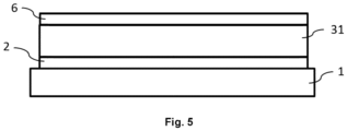
Fig. 5 schematically shows the layer sequence of the finished solar cell after applying a back contact (6) onto the activated absorber layer (31). - The embodiments of the invention described in the foregoing description are examples given by way of illustration and the invention is nowise limited thereto. Any modification, variation and equivalent arrangement as well as combinations of embodiments should be considered as being included within the scope of the invention.
-
- 1
- Substrate
- 2
- Front contact
- 3
- Absorber layer
- 31
- Activated absorber layer
- 4
- Polyvinylchloride film
- 5
- Cleaning solution
- 6
- Back contact
Claims (6)
- A method for activating an absorber layer of a semi-finished thin-film solar cell, the absorber layer comprising CdSexTe1-x, CdSe, CdS or CdTe, the method comprising the steps of- providing a semi-finished thin-film solar cell with an absorber layer comprising a CdSexTe1-x, layer or comprising at least two layers selected from CdS, CdTe, ZnTe, CdSe,- forming a polyvinylchloride film on a surface of the absorber layer, and- performing a heat treatment of the semi-finished thin-film solar cell with the polyvinylchloride film on it, wherein the temperature is in the range of 300°C to 500°C.
- The method of claim 1, characterized in that the polyvinylchloride film is formed by applying a solid sheet of polyvinylchloride on the surface of the absorber layer.
- The method of claim 1, characterized in that the polyvinylchloride film is formed by applying a solvent in which the polyvinylchloride is dissolved, followed by caking of the solvent.
- The method of claim 3, characterized in that the solvent is an organic solvent.
- The method of anyone of claims 1 to 4, characterized in that the method further comprises a cleaning step performed after the heat treatment in order to remove organic residuals resulting from the decomposed polyvinylchloride film.
- The method of claim 5, characterized in that at least one of the group comprising an aqueous anorganic acid, an organic complexing agent, an organic complexing acid, a mechanical cleaning device, a water jet, ultra sound or plasma clean is used within the cleaning step.
Applications Claiming Priority (2)
| Application Number | Priority Date | Filing Date | Title |
|---|---|---|---|
| CN202111393768.6A CN116154033A (en) | 2021-11-23 | 2021-11-23 | A method of activating the absorber layer of a thin film solar cell |
| PCT/CN2022/098045 WO2023092995A1 (en) | 2021-11-23 | 2022-06-10 | Method for activating absorption layer of thin-film solar cell |
Publications (3)
| Publication Number | Publication Date |
|---|---|
| EP4369423A1 true EP4369423A1 (en) | 2024-05-15 |
| EP4369423A4 EP4369423A4 (en) | 2025-04-02 |
| EP4369423B1 EP4369423B1 (en) | 2026-02-25 |
Family
ID=86353086
Family Applications (1)
| Application Number | Title | Priority Date | Filing Date |
|---|---|---|---|
| EP22897093.5A Active EP4369423B1 (en) | 2021-11-23 | 2022-06-10 | Method for activating absorption layer of thin-film solar cell |
Country Status (4)
| Country | Link |
|---|---|
| US (1) | US12563845B2 (en) |
| EP (1) | EP4369423B1 (en) |
| CN (1) | CN116154033A (en) |
| WO (1) | WO2023092995A1 (en) |
Families Citing this family (1)
| Publication number | Priority date | Publication date | Assignee | Title |
|---|---|---|---|---|
| CN120282578B (en) * | 2025-06-10 | 2025-08-22 | 邯郸中建材光电材料有限公司 | CdTe power generation glass and preparation method thereof |
Family Cites Families (13)
| Publication number | Priority date | Publication date | Assignee | Title |
|---|---|---|---|---|
| JPS61111585A (en) * | 1984-11-05 | 1986-05-29 | Matsushita Electric Ind Co Ltd | Photovoltaic cell manufacturing method and ink for photovoltaic cell manufacturing |
| JPS62143306A (en) * | 1985-12-11 | 1987-06-26 | 山本 隆一 | Metal sulfide |
| JP3366175B2 (en) * | 1996-02-20 | 2003-01-14 | 松下電池工業株式会社 | Method for manufacturing CdS / CdTe solar cell |
| EP1176644B1 (en) | 2000-07-26 | 2007-12-19 | ANTEC Solar Energy AG | Method to activate CdTe thin film solar cells |
| IT1396166B1 (en) | 2009-10-13 | 2012-11-16 | Arendi S P A | METHOD OF ACTIVATION OF THIN CDTE FILMS FOR APPLICATIONS IN SOLAR FILMS WITH THIN FILMS OF THE CDTE / CDS TYPE. |
| GB201019039D0 (en) * | 2010-11-11 | 2010-12-22 | Univ Durham | Method for doping a semi-conductor material and method for manufacturing solar cells |
| CN103811579B (en) * | 2014-02-13 | 2016-09-28 | 吉林大学 | A kind of flexible CdTe thin film solar cell and preparation method thereof |
| US9287439B1 (en) * | 2015-04-16 | 2016-03-15 | China Triumph International Engineering Co., Ltd. | Method of conditioning the CdTe layer of CdTe thin-film solar cells |
| CN108604617B (en) * | 2016-12-27 | 2022-06-28 | 中国建材国际工程集团有限公司 | Method for activating CdTe layers of CdTe thin film solar cells with calcium hypochlorite |
| EP3627564A1 (en) * | 2018-09-22 | 2020-03-25 | (CNBM) Bengbu Design & Research Institute for Glass Industry Co., Ltd. | Method for the post-treatment of an absorber layer |
| CN110098331B (en) * | 2019-04-17 | 2021-03-30 | 华南理工大学 | A kind of CdTe nanocrystalline film with surface passivation treatment and its surface passivation treatment method and application |
| CN114207842B (en) * | 2019-07-25 | 2024-01-30 | 中国建材国际工程集团有限公司 | Method for manufacturing inorganic thin film solar cell device and inorganic thin film solar cell device |
| CN112768558B (en) * | 2020-12-31 | 2022-08-16 | 中国建材国际工程集团有限公司 | Method for activating CdTe thin film solar cell |
-
2021
- 2021-11-23 CN CN202111393768.6A patent/CN116154033A/en active Pending
-
2022
- 2022-06-10 US US18/711,885 patent/US12563845B2/en active Active
- 2022-06-10 WO PCT/CN2022/098045 patent/WO2023092995A1/en not_active Ceased
- 2022-06-10 EP EP22897093.5A patent/EP4369423B1/en active Active
Also Published As
| Publication number | Publication date |
|---|---|
| US20250015219A1 (en) | 2025-01-09 |
| CN116154033A (en) | 2023-05-23 |
| EP4369423A4 (en) | 2025-04-02 |
| WO2023092995A1 (en) | 2023-06-01 |
| EP4369423B1 (en) | 2026-02-25 |
| US12563845B2 (en) | 2026-02-24 |
Similar Documents
| Publication | Publication Date | Title |
|---|---|---|
| US10707536B2 (en) | Solid-state laminate electrode assemblies and methods of making | |
| KR102409503B1 (en) | Photoactive devices and materials | |
| US9147792B2 (en) | Method of providing chloride treatment for a photovoltaic device and a chloride treated photovoltaic device | |
| US20140261685A1 (en) | Thin film photovoltaic device wtih large grain structure and methods of formation | |
| EP4369423B1 (en) | Method for activating absorption layer of thin-film solar cell | |
| EP3028295B1 (en) | Method for bonding substrates | |
| WO2014039420A1 (en) | In-situ tco chamber clean | |
| WO2017100443A1 (en) | Recovery of valuable or toxic metals from silicon solar cells | |
| FR2572739A1 (en) | PROCESS FOR INHIBITING CORROSION AFTER ETCHING OF ALUMINUM | |
| JP3893608B2 (en) | Annealed wafer manufacturing method | |
| RU2364574C2 (en) | Method for cleaning of substrate | |
| CN100499182C (en) | A process for large-scale production of CdTe/CdS thin film solar cells, without the use of CdCl2 | |
| DE112010003607T5 (en) | PHOVOLTAIK BACK CONTACT | |
| US9287439B1 (en) | Method of conditioning the CdTe layer of CdTe thin-film solar cells | |
| EP0178955A1 (en) | Process and apparatus for depositing upon a substrate a thin layer of a compound comprising at least one cationic and at least one anionic component | |
| US8592248B2 (en) | Etching method for use with thin-film photovoltaic panel | |
| EP2662899B1 (en) | Method for manufacturing a film of Cu2ZnSnS4 by SILAR | |
| WO2018119679A1 (en) | Method for activation of cdte layer of cdte thin-film solar cells with calcium hypochlorite | |
| EP3051596B1 (en) | Method for modifying cdte layer of cdte thin-layer solar cell | |
| CN106206244A (en) | The method that the CdTe layer of CdTe thin-layer solar cell is nursed one's health | |
| KR20010027459A (en) | Method of manufacturing a capacitor in a semiconductor device | |
| Ichimura et al. | Photochemical Deposition of Semiconductor Thin Films and Their Application for Solar Cells and Gas Sensors | |
| CN116262631A (en) | Method and apparatus for forming solid CdCl2 layers on thin film solar cells | |
| US20110147230A1 (en) | Film Removal | |
| WO2017114357A1 (en) | Method for removing transparent conductive oxide |
Legal Events
| Date | Code | Title | Description |
|---|---|---|---|
| STAA | Information on the status of an ep patent application or granted ep patent |
Free format text: STATUS: THE INTERNATIONAL PUBLICATION HAS BEEN MADE |
|
| PUAI | Public reference made under article 153(3) epc to a published international application that has entered the european phase |
Free format text: ORIGINAL CODE: 0009012 |
|
| STAA | Information on the status of an ep patent application or granted ep patent |
Free format text: STATUS: REQUEST FOR EXAMINATION WAS MADE |
|
| 17P | Request for examination filed |
Effective date: 20240205 |
|
| AK | Designated contracting states |
Kind code of ref document: A1 Designated state(s): AL AT BE BG CH CY CZ DE DK EE ES FI FR GB GR HR HU IE IS IT LI LT LU LV MC MK MT NL NO PL PT RO RS SE SI SK SM TR |
|
| RAP3 | Party data changed (applicant data changed or rights of an application transferred) |
Owner name: CTF SOLAR GMBH Owner name: CHINA TRIUMPH INTERNATIONAL ENGINEERING CO., LTD. |
|
| RIN1 | Information on inventor provided before grant (corrected) |
Inventor name: DROST, CHRISTIAN Inventor name: YIN, XINJIAN Inventor name: MA, LIYUN Inventor name: FU, GANHUA Inventor name: PENG, SHOU |
|
| DAV | Request for validation of the european patent (deleted) | ||
| DAX | Request for extension of the european patent (deleted) | ||
| REG | Reference to a national code |
Ref country code: DE Ref legal event code: R079 Free format text: PREVIOUS MAIN CLASS: H01L0031180000 Ipc: H10F0010162000 Ref country code: DE Ref legal event code: R079 Ref document number: 602022031359 Country of ref document: DE Free format text: PREVIOUS MAIN CLASS: H01L0031180000 Ipc: H10F0010162000 |
|
| A4 | Supplementary search report drawn up and despatched |
Effective date: 20250305 |
|
| RIC1 | Information provided on ipc code assigned before grant |
Ipc: H10F 71/00 20250101ALI20250227BHEP Ipc: H10F 10/162 20250101AFI20250227BHEP |
|
| GRAP | Despatch of communication of intention to grant a patent |
Free format text: ORIGINAL CODE: EPIDOSNIGR1 |
|
| STAA | Information on the status of an ep patent application or granted ep patent |
Free format text: STATUS: GRANT OF PATENT IS INTENDED |
|
| RIC1 | Information provided on ipc code assigned before grant |
Ipc: H10F 10/162 20250101AFI20250910BHEP Ipc: H10F 71/00 20250101ALI20250910BHEP |
|
| INTG | Intention to grant announced |
Effective date: 20250922 |
|
| GRAS | Grant fee paid |
Free format text: ORIGINAL CODE: EPIDOSNIGR3 |
|
| GRAA | (expected) grant |
Free format text: ORIGINAL CODE: 0009210 |
|
| STAA | Information on the status of an ep patent application or granted ep patent |
Free format text: STATUS: THE PATENT HAS BEEN GRANTED |
|
| AK | Designated contracting states |
Kind code of ref document: B1 Designated state(s): AL AT BE BG CH CY CZ DE DK EE ES FI FR GB GR HR HU IE IS IT LI LT LU LV MC MK MT NL NO PL PT RO RS SE SI SK SM TR |
|
| REG | Reference to a national code |
Ref country code: CH Ref legal event code: F10 Free format text: ST27 STATUS EVENT CODE: U-0-0-F10-F00 (AS PROVIDED BY THE NATIONAL OFFICE) Effective date: 20260225 Ref country code: GB Ref legal event code: FG4D |
|
| REG | Reference to a national code |
Ref country code: DE Ref legal event code: R096 Ref document number: 602022031359 Country of ref document: DE |
|
| REG | Reference to a national code |
Ref country code: IE Ref legal event code: FG4D |