EP4369401A1 - Esd protection circuit for negative voltage operation - Google Patents
Esd protection circuit for negative voltage operation Download PDFInfo
- Publication number
- EP4369401A1 EP4369401A1 EP23203845.5A EP23203845A EP4369401A1 EP 4369401 A1 EP4369401 A1 EP 4369401A1 EP 23203845 A EP23203845 A EP 23203845A EP 4369401 A1 EP4369401 A1 EP 4369401A1
- Authority
- EP
- European Patent Office
- Prior art keywords
- pin
- diode
- chip
- type
- type transistor
- Prior art date
- Legal status (The legal status is an assumption and is not a legal conclusion. Google has not performed a legal analysis and makes no representation as to the accuracy of the status listed.)
- Pending
Links
- 238000009792 diffusion process Methods 0.000 claims abstract description 19
- 238000001514 detection method Methods 0.000 claims description 24
- XUIMIQQOPSSXEZ-UHFFFAOYSA-N Silicon Chemical compound [Si] XUIMIQQOPSSXEZ-UHFFFAOYSA-N 0.000 claims description 2
- 229910052710 silicon Inorganic materials 0.000 claims description 2
- 239000010703 silicon Substances 0.000 claims description 2
- 238000010586 diagram Methods 0.000 description 14
- 238000000034 method Methods 0.000 description 8
- 238000002955 isolation Methods 0.000 description 5
- 238000004519 manufacturing process Methods 0.000 description 5
- 239000004065 semiconductor Substances 0.000 description 5
- 239000002019 doping agent Substances 0.000 description 2
- 239000000758 substrate Substances 0.000 description 2
- ZOXJGFHDIHLPTG-UHFFFAOYSA-N Boron Chemical compound [B] ZOXJGFHDIHLPTG-UHFFFAOYSA-N 0.000 description 1
- GYHNNYVSQQEPJS-UHFFFAOYSA-N Gallium Chemical compound [Ga] GYHNNYVSQQEPJS-UHFFFAOYSA-N 0.000 description 1
- OAICVXFJPJFONN-UHFFFAOYSA-N Phosphorus Chemical compound [P] OAICVXFJPJFONN-UHFFFAOYSA-N 0.000 description 1
- 230000004075 alteration Effects 0.000 description 1
- 229910052782 aluminium Inorganic materials 0.000 description 1
- XAGFODPZIPBFFR-UHFFFAOYSA-N aluminium Chemical compound [Al] XAGFODPZIPBFFR-UHFFFAOYSA-N 0.000 description 1
- 229910052785 arsenic Inorganic materials 0.000 description 1
- RQNWIZPPADIBDY-UHFFFAOYSA-N arsenic atom Chemical compound [As] RQNWIZPPADIBDY-UHFFFAOYSA-N 0.000 description 1
- 229910052796 boron Inorganic materials 0.000 description 1
- 239000003990 capacitor Substances 0.000 description 1
- 229910052733 gallium Inorganic materials 0.000 description 1
- 238000012986 modification Methods 0.000 description 1
- 230000004048 modification Effects 0.000 description 1
- 230000003071 parasitic effect Effects 0.000 description 1
- 229910052698 phosphorus Inorganic materials 0.000 description 1
- 239000011574 phosphorus Substances 0.000 description 1
Images



Classifications
-
- H—ELECTRICITY
- H10—SEMICONDUCTOR DEVICES; ELECTRIC SOLID-STATE DEVICES NOT OTHERWISE PROVIDED FOR
- H10D—INORGANIC ELECTRIC SEMICONDUCTOR DEVICES
- H10D89/00—Aspects of integrated devices not covered by groups H10D84/00 - H10D88/00
- H10D89/60—Integrated devices comprising arrangements for electrical or thermal protection, e.g. protection circuits against electrostatic discharge [ESD]
- H10D89/601—Integrated devices comprising arrangements for electrical or thermal protection, e.g. protection circuits against electrostatic discharge [ESD] for devices having insulated gate electrodes, e.g. for IGFETs or IGBTs
- H10D89/611—Integrated devices comprising arrangements for electrical or thermal protection, e.g. protection circuits against electrostatic discharge [ESD] for devices having insulated gate electrodes, e.g. for IGFETs or IGBTs using diodes as protective elements
-
- H—ELECTRICITY
- H10—SEMICONDUCTOR DEVICES; ELECTRIC SOLID-STATE DEVICES NOT OTHERWISE PROVIDED FOR
- H10D—INORGANIC ELECTRIC SEMICONDUCTOR DEVICES
- H10D89/00—Aspects of integrated devices not covered by groups H10D84/00 - H10D88/00
- H10D89/60—Integrated devices comprising arrangements for electrical or thermal protection, e.g. protection circuits against electrostatic discharge [ESD]
- H10D89/601—Integrated devices comprising arrangements for electrical or thermal protection, e.g. protection circuits against electrostatic discharge [ESD] for devices having insulated gate electrodes, e.g. for IGFETs or IGBTs
- H10D89/811—Integrated devices comprising arrangements for electrical or thermal protection, e.g. protection circuits against electrostatic discharge [ESD] for devices having insulated gate electrodes, e.g. for IGFETs or IGBTs using FETs as protective elements
- H10D89/819—Bias arrangements for gate electrodes of FETs, e.g. RC networks or voltage partitioning circuits
-
- H—ELECTRICITY
- H10—SEMICONDUCTOR DEVICES; ELECTRIC SOLID-STATE DEVICES NOT OTHERWISE PROVIDED FOR
- H10D—INORGANIC ELECTRIC SEMICONDUCTOR DEVICES
- H10D89/00—Aspects of integrated devices not covered by groups H10D84/00 - H10D88/00
- H10D89/60—Integrated devices comprising arrangements for electrical or thermal protection, e.g. protection circuits against electrostatic discharge [ESD]
- H10D89/601—Integrated devices comprising arrangements for electrical or thermal protection, e.g. protection circuits against electrostatic discharge [ESD] for devices having insulated gate electrodes, e.g. for IGFETs or IGBTs
- H10D89/711—Integrated devices comprising arrangements for electrical or thermal protection, e.g. protection circuits against electrostatic discharge [ESD] for devices having insulated gate electrodes, e.g. for IGFETs or IGBTs using bipolar transistors as protective elements
- H10D89/713—Integrated devices comprising arrangements for electrical or thermal protection, e.g. protection circuits against electrostatic discharge [ESD] for devices having insulated gate electrodes, e.g. for IGFETs or IGBTs using bipolar transistors as protective elements including a PNP transistor and a NPN transistor, wherein each of said transistors has its base region coupled to the collector region of the other transistor, e.g. silicon controlled rectifier [SCR] devices
-
- H—ELECTRICITY
- H10—SEMICONDUCTOR DEVICES; ELECTRIC SOLID-STATE DEVICES NOT OTHERWISE PROVIDED FOR
- H10D—INORGANIC ELECTRIC SEMICONDUCTOR DEVICES
- H10D89/00—Aspects of integrated devices not covered by groups H10D84/00 - H10D88/00
- H10D89/60—Integrated devices comprising arrangements for electrical or thermal protection, e.g. protection circuits against electrostatic discharge [ESD]
- H10D89/601—Integrated devices comprising arrangements for electrical or thermal protection, e.g. protection circuits against electrostatic discharge [ESD] for devices having insulated gate electrodes, e.g. for IGFETs or IGBTs
- H10D89/811—Integrated devices comprising arrangements for electrical or thermal protection, e.g. protection circuits against electrostatic discharge [ESD] for devices having insulated gate electrodes, e.g. for IGFETs or IGBTs using FETs as protective elements
Definitions
- one or more ESD protection circuits are designed within the die to pass a human body model (HBM) and charged device model (CDM) of ESD specifications.
- HBM human body model
- CDM charged device model
- one or more diodes serving as the ESD protection circuit are connected between an input/output (I/O) pin and a ground voltage, and these diodes absorb the short-duration voltage pulses during the ESD strike, that is high peak currents from the ESD strike flow to the ground through the diodes and limit the ESD strike voltages from damaging the internal circuits.
- the ESD protection circuit having diodes when used for the I/O pin having negative voltage, a parasitic diode may be formed between the I/O pin and the ground voltage so that a junction forward leakage current is generated.
- the conventional art uses a deep N-well isolation technique to isolate the P-type diffusion of the first diode and the N-type diffusion of the last diode.
- the deep N-well process and mask will increase the manufacturing costs.
- a chip comprising an I/O pin and an ESD protection circuit.
- the ESD protection circuit comprises a P-type device and a first diode, wherein the P-type device is coupled between the I/O pin and a ground voltage, and an anode of the first diode is directly connected to the I/O pin.
- the ESD protection circuit does not comprise any device whose N-type doping/diffusion is directly connected to the I/O pin.
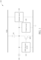
- FIG. 1 is a diagram illustrating a chip 100 according to one embodiment of the present invention.
- the chip 100 comprises an I/O pin 102, an ESD detection circuit 110, a control circuit 120, an internal circuit 130, and an ESD protection circuit comprising a P-type transistor MP1 and at least one diode D1, wherein the I/O pin 102 is used to receive a negative voltage from a device external to the chip 100, and the negative voltage is lower than a ground voltage, for example, the negative voltage may be -1V.
- the P-type transistor MP1 and the diode D1 serves as the ESD protection circuit to absorb the short-duration voltage pulses during the ESD strike, wherein a drain electrode of the P-type transistor MP1 is directly connected to the I/O pin 102 without passing through any other circuit element, and a source electrode of the P-type transistor MP1 is coupled to the ground voltage, that is, there may or may not be other circuit element(s) between the source electrode and the ground voltage; an anode of the diode D1 is directly connected to the I/O pin 102 without passing through any other circuit element, and a cathode of the diode D1 is coupled to a supply voltage VDD, that is, there may or may not be other circuit element (s) between the cathode of the diode D1 and the supply voltage VDD.
- the ESD detection circuit 110 is configured to detect a voltage level of the I/O pin 102 to determine if enabling the P-type transistor MP1, that is, if the I/O pin 102 suffers ESD strikes, the ESD detection circuit 110 generates a control signal to enable the P-type transistor MP1 to form a current path; and the P-type transistor MP1 is disabled when the I/O pin 102 has the normal negative voltage.
- a bulk of the P-type transistor MP1 is connected to its source electrode or a bias voltage provided by the control circuit 120, wherein the control circuit 120 is an optional device that can be removed from the chip 100.
- the I/O pin 102 only connects to the anode of the diode D1 and the drain electrode of the P-type transistor MP1, without connecting to the cathode of any diode or source/drain electrode of any N-type transistor. Therefore, since the I/O pin 102 only connects to the P-type doping/diffusion (e.g., boron, aluminum, gallium or any other P-type dopant) of the semiconductor device, without directly connecting to any N-type doping/diffusion (e.g., phosphorus, arsenic or any other N-type dopant), a junction forward leakage current from the ground to the I/O pin 102 will not be generated, so that a power consumption of the chip 100 can be improved. In addition, because there is no need to use the deep N-well isolation technique in the ESD protection circuit, the manufacturing cost will not increase.
- P-type doping/diffusion e.g., boron, aluminum, gallium or any other P-type dopant
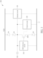
- FIG. 2 is a diagram illustrating a chip 200 according to one embodiment of the present invention.
- the chip 200 comprises an I/O pin 202, an ESD detection circuit 210, a control circuit 220, an internal circuit 230, and an ESD protection circuit comprising a P-type transistor MP1 and at least one diode D2, wherein the I/O pin 202 is used to receive a negative voltage from a device external to the chip 200, and the negative voltage is lower than the ground voltage.
- the P-type transistor MP1 and the diode D2 serves as the ESD protection circuit to absorb the short-duration voltage pulses during the ESD strike, wherein a drain electrode of the P-type transistor MP1 is directly connected to the I/O pin 202 without passing through any other circuit element, and a source electrode of the P-type transistor MP1 is coupled to the ground voltage, that is, there may or may not be other circuit element(s) between the source electrode and the ground voltage; an anode of the diode D2 is directly connected to the I/O pin 202 without passing through any other circuit element, and a cathode of the diode D2 is coupled to the ground voltage , that is, there may or may not be other circuit element(s) between the cathode of the diode D2 and the ground voltage.
- the ESD detection circuit 210 is configured to detect a voltage level of the I/O pin 202 to determine if enabling the P-type transistor MP1, that is, if the I/O pin 202 suffers ESD strikes, the ESD detection circuit 210 enables the P-type transistor MP1 to form a current path; and the P-type transistor MP1 is disabled when the I/O pin 202 has the normal negative voltage.
- a bulk of the P-type transistor MP1 is connected to its source electrode or a bias voltage provided by the control circuit 220, wherein the control circuit 220 is an optional device that can be removed from the chip 200.
- the I/O pin 202 only connects to the anode of the diode D2 and the drain electrode of the P-type transistor MP1, without connecting to the cathode of any diode or source/drain electrode of any N-type transistor. Therefore, since the I/O pin 202 only connects to the P-type doping/diffusion of the semiconductor device, without directly connecting to any N-type doping/diffusion, a junction forward leakage current from the ground to the I/O pin 202 will not be generated, so that a power consumption of the chip 200 can be improved. In addition, because there is no need to use the deep N-well isolation technique in the ESD protection circuit, the manufacturing cost will not increase.
- FIG. 3 is a diagram illustrating a chip 300 according to one embodiment of the present invention.
- the chip 300 comprises an I/O pin 302, an ESD detection circuit 310, a control circuit 320, an internal circuit 330, and an ESD protection circuit comprising a P-type transistor MP1 and a plurality of diodes such as D3 - D5, wherein the I/O pin 302 is used to receive a negative voltage from a device external to the chip 300, and the negative voltage is lower than the ground voltage.
- the P-type transistor MP1 and the diodes D3 - D5 serves as the ESD protection circuit to absorb the short-duration voltage pulses during the ESD strike, wherein a drain electrode of the P-type transistor MP1 is directly connected to the I/O pin 302 without passing through any other circuit element, and a source electrode of the P-type transistor MP1 is coupled to the ground voltage via the diode D5.
- an anode of the diode D5 is connected to the ground voltage
- a cathode of the diode D5 is coupled to the source electrode of the P-type transistor, wherein there may or may not be other circuit element (s) between the source electrode and the diode D5.
- the diodes D3 and D4 form a diode string, wherein an anode of the diode D3 is directly connected to the I/O pin 302 without passing through any other circuit element, and a cathode of the diode D4 is coupled to a supply voltage VDD, and there may or may not be other diode (s) between the diodes D3 and D4.
- the ESD detection circuit 310 is configured to detect a voltage level of the I/O pin 302 to determine if enabling the P-type transistor MP1, that is, if the I/O pin 302 suffers ESD strikes, the ESD detection circuit 310 enables the P-type transistor MP1 to form a current path; and the P-type transistor MP1 is disabled when the I/O pin 302 has the normal negative voltage.
- a bulk of the P-type transistor MP1 is connected to its source electrode or a bias voltage provided by the control circuit 320, wherein the control circuit 320 is an optional device that can be removed from the chip 300.
- the I/O pin 302 only connects directly to the anode of the diode D3 and the drain electrode of the P-type transistor MP1, without connecting directly to the cathode of any diode or source/drain electrode of any N-type transistor. Therefore, since the I/O pin 302 only connects to the P-type doping/diffusion of the semiconductor device, without directly connecting to any N-type doping/diffusion, a junction forward leakage current from the ground to the I/O pin 302 will not be generated, so that a power consumption of the chip 300 can be improved. In addition, because there is no need to use the deep N-well isolation technique in the ESD protection circuit, the manufacturing cost will not increase.
- FIG. 4 is a diagram illustrating a chip 400 according to one embodiment of the present invention.
- the chip 400 comprises an I/O pin 402, an ESD detection circuit 410, a control circuit 420, an internal circuit 430, and an ESD protection circuit comprising a P-type transistor MP1 and a plurality of diodes such as D6 - D8, wherein the I/O pin 402 is used to receive a negative voltage from a device external to the chip 400, and the negative voltage is lower than the ground voltage.
- the P-type transistor MP1 and the diodes D6 - D8 serves as the ESD protection circuit to absorb the short-duration voltage pulses during the ESD strike, wherein a drain electrode of the P-type transistor MP1 is directly connected to the I/O pin 402 without passing through any other circuit element, and a source electrode of the P-type transistor MP1 is coupled to the ground voltage via the diode D8.
- an anode of the diode D8 is connected to the ground voltage
- a cathode of the diode D8 is coupled to the source electrode of the P-type transistor, wherein there may or may not be other circuit element (s) between the source electrode and the diode D8.
- the diodes D6 and D7 form a diode string, wherein an anode of the diode D6 is directly connected to the I/O pin 402 without passing through any other circuit element, and a cathode of the diode D7 is coupled to the ground voltage, and there may or may not be other diode (s) between the diodes D6 and D7.
- the ESD detection circuit 410 is configured to detect a voltage level of the I/O pin 402 to determine if enabling the P-type transistor MP1, that is, if the I/O pin 402 suffers ESD strikes, the ESD detection circuit 410 enables the P-type transistor MP1 to form a current path; and the P-type transistor MP1 is disabled when the I/O pin 402 has the normal negative voltage.
- a bulk of the P-type transistor MP1 is connected to its source electrode or a bias voltage provided by the control circuit 420, wherein the control circuit 420 is an optional device that can be removed from the chip 400.
- the I/O pin 402 only connects directly to the anode of the diode D6 and the drain electrode of the P-type transistor MP1, without connecting directly to the cathode of any diode or source/drain electrode of any N-type transistor. Therefore, since the I/O pin 402 only connects to the P-type doping/diffusion of the semiconductor device, without directly connecting to any N-type doping/diffusion, a junction forward leakage current from the ground to the I/O pin 402 will not be generated, so that a power consumption of the chip 400 can be improved. In addition, because there is no need to use the deep N-well isolation technique in the ESD protection circuit, the manufacturing cost will not increase.
- FIG. 5 is a diagram illustrating the ESD detection circuit 410, the control circuit 420 and part of the internal circuit 430 according to one embodiment of the present invention.
- the ESD detection circuit 410 and the control circuit 420 comprise a resistor R, a P-type transistor MP2 serving as s metal-oxide-semiconductor capacitor and a plurality of P-type transistors MP3 - MP5, wherein a gate electrode of the P-type transistor MP2 is coupled to the I/O pin 402 via the resistor R, a drain electrode of the P-type transistor MP3 is directly connected to the I/O pin 402, a source electrode of the P-type transistor MP3 is coupled to a drain electrode of the P-type transistor MP4 and a gate electrode of the P-type transistor MP5, and a bulks of the P-type transistors MP1 - MP5 and source electrodes of the P-type transistors MP1, MP2 and MP4 are connected together.
- the I/O pin 402 only connects directly to the drain electrode of the P-type transistor and a gate electrode of the transistor, without connecting directly to the cathode of any diode or source/drain electrode of any N-type transistor.
- the embodiments of the ESD detection circuit 410, the control circuit 420 and part of the internal circuit 430 shown in FIG. 5 are for illustrative, not a limitation of the present invention, as long as the ESD detection circuit 410 can detect a voltage level of the I/O pin 402 to determine if enabling the P-type transistor MP1, the ESD detection circuit 410, the control circuit 420 and part of the internal circuit 430 can have any suitable designs.
- the embodiments of the ESD detection circuit 410, the control circuit 420 and part of the internal circuit 430 shown in FIG. 5 can be used to implement the ESD detection circuit 110/210/310, the control circuit 120/220/320 and part of the internal circuit 130/230/330 shown in FIG. 1 , FIG. 2 or FIG. 3 .
- FIG. 6 is a diagram illustrating a chip 600 according to one embodiment of the present invention.
- the chip 600 comprises an I/O pin 602, a control circuit 620, an internal circuit 630, and an ESD protection circuit comprising a P-type field-oxide device (PFOD) and at least one diode D9, wherein the I/O pin 602 is used to receive a negative voltage from a device external to the chip 600, and the negative voltage is lower than a ground voltage.
- PFOD P-type field-oxide device
- the PFOD and the diode D9 serves as the ESD protection circuit to absorb the short-duration voltage pulses during the ESD strike, wherein the PFOD is directly connected to the I/O pin 602 without passing through any other circuit element; an anode of the diode D9 is directly connected to the I/O pin 602 without passing through any other circuit element, and a cathode of the diode D9 is coupled to a supply voltage VDD, that is, there may or may not be other circuit element (s) between the cathode of the diode D9 and the supply voltage VDD.
- a bulk of the PFOD is connected to a bias voltage provided by the control circuit 620.
- the diode D2 shown in FIG. 2 , the diodes D3 - D5 shown in FIG. 3 , the diodes D6 - D8 shown in FIG. 4 can be applied to the chip 600. These alternative designs shall fall within the scope of the present invention.
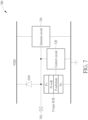
- FIG. 7 is a diagram illustrating a chip 700 according to one embodiment of the present invention.
- the chip 700 comprises an I/O pin 702, a control circuit 720, an internal circuit 730, and an ESD protection circuit comprising a P-type silicon controlled rectifier (SCR) and at least one diode D10, wherein the I/O pin 702 is used to receive a negative voltage from a device external to the chip 700, and the negative voltage is lower than a ground voltage.
- SCR P-type silicon controlled rectifier
- the P-type SCR and the diode D10 serves as the ESD protection circuit to absorb the short-duration voltage pulses during the ESD strike.
- the P-type SCR comprises P+ diffusion, N-well, P-type substrate and N+ diffusion, wherein the P+ diffusion is directly connected to the I/O pin 702 without passing through any other circuit element, and the N+ diffusion is coupled to the ground voltage.
- An anode of the diode D10 is directly connected to the I/O pin 702 without passing through any other circuit element, and a cathode of the diode D10 is coupled to a supply voltage VDD, that is, there may or may not be other circuit element(s) between the cathode of the diode D10 and the supply voltage VDD.
- the P-type substrate is connected to a bias voltage provided by the control circuit 720.
- the diode D2 shown in FIG. 2 , the diodes D3 - D5 shown in FIG. 3 , the diodes D6 - D8 shown in FIG. 4 can be applied to the chip 700. These alternative designs shall fall within the scope of the present invention.
Landscapes
- Semiconductor Integrated Circuits (AREA)
- Metal-Oxide And Bipolar Metal-Oxide Semiconductor Integrated Circuits (AREA)
Abstract
Description
- This application claims the benefit of
U.S. Provisional Application No. 63/382,892, filed on November 9th, 2022 - In order to protect internal circuits of a die from being damaged by electrostatic discharge (ESD), one or more ESD protection circuits are designed within the die to pass a human body model (HBM) and charged device model (CDM) of ESD specifications. In the conventional art, one or more diodes serving as the ESD protection circuit are connected between an input/output (I/O) pin and a ground voltage, and these diodes absorb the short-duration voltage pulses during the ESD strike, that is high peak currents from the ESD strike flow to the ground through the diodes and limit the ESD strike voltages from damaging the internal circuits.
- However, when the ESD protection circuit having diodes is used for the I/O pin having negative voltage, a parasitic diode may be formed between the I/O pin and the ground voltage so that a junction forward leakage current is generated. To solve this problem, the conventional art uses a deep N-well isolation technique to isolate the P-type diffusion of the first diode and the N-type diffusion of the last diode. However, the deep N-well process and mask will increase the manufacturing costs.
- It is therefore an objective of the present invention to provide a ESD protection circuit for the I/O pin having a negative voltage, which can avoid leakage current without using deep N-well process, to solve the above-mentioned problems.
- According to one embodiment of the present invention, a chip comprising an I/O pin and an ESD protection circuit is disclosed. The ESD protection circuit comprises a P-type device and a first diode, wherein the P-type device is coupled between the I/O pin and a ground voltage, and an anode of the first diode is directly connected to the I/O pin. In addition, the ESD protection circuit does not comprise any device whose N-type doping/diffusion is directly connected to the I/O pin.
- These and other objectives of the present invention will no doubt become obvious to those of ordinary skill in the art after reading the following detailed description of the preferred embodiment that is illustrated in the various figures and drawings.
-
-
FIG. 1 is a diagram illustrating a chip according to a first embodiment of the present invention. -
FIG. 2 is a diagram illustrating a chip according to a second embodiment of the present invention. -
FIG. 3 is a diagram illustrating a chip according to a third embodiment of the present invention. -
FIG. 4 is a diagram illustrating a chip according to a fourth embodiment of the present invention. -
FIG. 5 is a diagram illustrating the ESD detection circuit, the control circuit and part of the internal circuit according to one embodiment of the present invention. -
FIG. 6 is a diagram illustrating a chip according to a fifth embodiment of the present invention. -
FIG. 7 is a diagram illustrating a chip according to a sixth embodiment of the present invention. - Certain terms are used throughout the following description and claims to refer to particular system components. As one skilled in the art will appreciate, manufacturers may refer to a component by different names. This document does not intend to distinguish between components that differ in name but not function. In the following discussion and in the claims, the terms "including" and "comprising" are used in an open-ended fashion, and thus should be interpreted to mean "including, but not limited to ...". The terms "couple" and "couples" are intended to mean either an indirect or a direct electrical connection. Thus, if a first device couples to a second device, that connection may be through a direct electrical connection, or through an indirect electrical connection via other devices and connections.
-
FIG. 1 is a diagram illustrating achip 100 according to one embodiment of the present invention. As shown inFIG. 1 , thechip 100 comprises an I/O pin 102, anESD detection circuit 110, acontrol circuit 120, aninternal circuit 130, and an ESD protection circuit comprising a P-type transistor MP1 and at least one diode D1, wherein the I/O pin 102 is used to receive a negative voltage from a device external to thechip 100, and the negative voltage is lower than a ground voltage, for example, the negative voltage may be -1V. - In the embodiment shown in
FIG. 1 , the P-type transistor MP1 and the diode D1 serves as the ESD protection circuit to absorb the short-duration voltage pulses during the ESD strike, wherein a drain electrode of the P-type transistor MP1 is directly connected to the I/O pin 102 without passing through any other circuit element, and a source electrode of the P-type transistor MP1 is coupled to the ground voltage, that is, there may or may not be other circuit element(s) between the source electrode and the ground voltage; an anode of the diode D1 is directly connected to the I/O pin 102 without passing through any other circuit element, and a cathode of the diode D1 is coupled to a supply voltage VDD, that is, there may or may not be other circuit element (s) between the cathode of the diode D1 and the supply voltage VDD. TheESD detection circuit 110 is configured to detect a voltage level of the I/O pin 102 to determine if enabling the P-type transistor MP1, that is, if the I/O pin 102 suffers ESD strikes, theESD detection circuit 110 generates a control signal to enable the P-type transistor MP1 to form a current path; and the P-type transistor MP1 is disabled when the I/O pin 102 has the normal negative voltage. In addition, a bulk of the P-type transistor MP1 is connected to its source electrode or a bias voltage provided by thecontrol circuit 120, wherein thecontrol circuit 120 is an optional device that can be removed from thechip 100. - In this embodiment, the I/
O pin 102 only connects to the anode of the diode D1 and the drain electrode of the P-type transistor MP1, without connecting to the cathode of any diode or source/drain electrode of any N-type transistor. Therefore, since the I/O pin 102 only connects to the P-type doping/diffusion (e.g., boron, aluminum, gallium or any other P-type dopant) of the semiconductor device, without directly connecting to any N-type doping/diffusion (e.g., phosphorus, arsenic or any other N-type dopant), a junction forward leakage current from the ground to the I/O pin 102 will not be generated, so that a power consumption of thechip 100 can be improved. In addition, because there is no need to use the deep N-well isolation technique in the ESD protection circuit, the manufacturing cost will not increase. -
FIG. 2 is a diagram illustrating achip 200 according to one embodiment of the present invention. As shown inFIG. 2 , thechip 200 comprises an I/O pin 202, anESD detection circuit 210, acontrol circuit 220, aninternal circuit 230, and an ESD protection circuit comprising a P-type transistor MP1 and at least one diode D2, wherein the I/O pin 202 is used to receive a negative voltage from a device external to thechip 200, and the negative voltage is lower than the ground voltage. - In the embodiment shown in
FIG. 2 , the P-type transistor MP1 and the diode D2 serves as the ESD protection circuit to absorb the short-duration voltage pulses during the ESD strike, wherein a drain electrode of the P-type transistor MP1 is directly connected to the I/O pin 202 without passing through any other circuit element, and a source electrode of the P-type transistor MP1 is coupled to the ground voltage, that is, there may or may not be other circuit element(s) between the source electrode and the ground voltage; an anode of the diode D2 is directly connected to the I/O pin 202 without passing through any other circuit element, and a cathode of the diode D2 is coupled to the ground voltage , that is, there may or may not be other circuit element(s) between the cathode of the diode D2 and the ground voltage. TheESD detection circuit 210 is configured to detect a voltage level of the I/O pin 202 to determine if enabling the P-type transistor MP1, that is, if the I/O pin 202 suffers ESD strikes, theESD detection circuit 210 enables the P-type transistor MP1 to form a current path; and the P-type transistor MP1 is disabled when the I/O pin 202 has the normal negative voltage. In addition, a bulk of the P-type transistor MP1 is connected to its source electrode or a bias voltage provided by thecontrol circuit 220, wherein thecontrol circuit 220 is an optional device that can be removed from thechip 200. - In this embodiment, the I/
O pin 202 only connects to the anode of the diode D2 and the drain electrode of the P-type transistor MP1, without connecting to the cathode of any diode or source/drain electrode of any N-type transistor. Therefore, since the I/O pin 202 only connects to the P-type doping/diffusion of the semiconductor device, without directly connecting to any N-type doping/diffusion, a junction forward leakage current from the ground to the I/O pin 202 will not be generated, so that a power consumption of thechip 200 can be improved. In addition, because there is no need to use the deep N-well isolation technique in the ESD protection circuit, the manufacturing cost will not increase. -
FIG. 3 is a diagram illustrating achip 300 according to one embodiment of the present invention. As shown inFIG. 3 , thechip 300 comprises an I/O pin 302, anESD detection circuit 310, acontrol circuit 320, aninternal circuit 330, and an ESD protection circuit comprising a P-type transistor MP1 and a plurality of diodes such as D3 - D5, wherein the I/O pin 302 is used to receive a negative voltage from a device external to thechip 300, and the negative voltage is lower than the ground voltage. - In the embodiment shown in
FIG. 3 , the P-type transistor MP1 and the diodes D3 - D5 serves as the ESD protection circuit to absorb the short-duration voltage pulses during the ESD strike, wherein a drain electrode of the P-type transistor MP1 is directly connected to the I/O pin 302 without passing through any other circuit element, and a source electrode of the P-type transistor MP1 is coupled to the ground voltage via the diode D5. In this embodiment, an anode of the diode D5 is connected to the ground voltage, a cathode of the diode D5 is coupled to the source electrode of the P-type transistor, wherein there may or may not be other circuit element (s) between the source electrode and the diode D5. The diodes D3 and D4 form a diode string, wherein an anode of the diode D3 is directly connected to the I/O pin 302 without passing through any other circuit element, and a cathode of the diode D4 is coupled to a supply voltage VDD, and there may or may not be other diode (s) between the diodes D3 and D4. TheESD detection circuit 310 is configured to detect a voltage level of the I/O pin 302 to determine if enabling the P-type transistor MP1, that is, if the I/O pin 302 suffers ESD strikes, theESD detection circuit 310 enables the P-type transistor MP1 to form a current path; and the P-type transistor MP1 is disabled when the I/O pin 302 has the normal negative voltage. In addition, a bulk of the P-type transistor MP1 is connected to its source electrode or a bias voltage provided by thecontrol circuit 320, wherein thecontrol circuit 320 is an optional device that can be removed from thechip 300. - In this embodiment, the I/
O pin 302 only connects directly to the anode of the diode D3 and the drain electrode of the P-type transistor MP1, without connecting directly to the cathode of any diode or source/drain electrode of any N-type transistor. Therefore, since the I/O pin 302 only connects to the P-type doping/diffusion of the semiconductor device, without directly connecting to any N-type doping/diffusion, a junction forward leakage current from the ground to the I/O pin 302 will not be generated, so that a power consumption of thechip 300 can be improved. In addition, because there is no need to use the deep N-well isolation technique in the ESD protection circuit, the manufacturing cost will not increase. -
FIG. 4 is a diagram illustrating achip 400 according to one embodiment of the present invention. As shown inFIG. 4 , thechip 400 comprises an I/O pin 402, anESD detection circuit 410, acontrol circuit 420, aninternal circuit 430, and an ESD protection circuit comprising a P-type transistor MP1 and a plurality of diodes such as D6 - D8, wherein the I/O pin 402 is used to receive a negative voltage from a device external to thechip 400, and the negative voltage is lower than the ground voltage. - In the embodiment shown in
FIG. 4 , the P-type transistor MP1 and the diodes D6 - D8 serves as the ESD protection circuit to absorb the short-duration voltage pulses during the ESD strike, wherein a drain electrode of the P-type transistor MP1 is directly connected to the I/O pin 402 without passing through any other circuit element, and a source electrode of the P-type transistor MP1 is coupled to the ground voltage via the diode D8. In this embodiment, an anode of the diode D8 is connected to the ground voltage, a cathode of the diode D8 is coupled to the source electrode of the P-type transistor, wherein there may or may not be other circuit element (s) between the source electrode and the diode D8. The diodes D6 and D7 form a diode string, wherein an anode of the diode D6 is directly connected to the I/O pin 402 without passing through any other circuit element, and a cathode of the diode D7 is coupled to the ground voltage, and there may or may not be other diode (s) between the diodes D6 and D7. TheESD detection circuit 410 is configured to detect a voltage level of the I/O pin 402 to determine if enabling the P-type transistor MP1, that is, if the I/O pin 402 suffers ESD strikes, theESD detection circuit 410 enables the P-type transistor MP1 to form a current path; and the P-type transistor MP1 is disabled when the I/O pin 402 has the normal negative voltage. In addition, a bulk of the P-type transistor MP1 is connected to its source electrode or a bias voltage provided by thecontrol circuit 420, wherein thecontrol circuit 420 is an optional device that can be removed from thechip 400. - In this embodiment, the I/
O pin 402 only connects directly to the anode of the diode D6 and the drain electrode of the P-type transistor MP1, without connecting directly to the cathode of any diode or source/drain electrode of any N-type transistor. Therefore, since the I/O pin 402 only connects to the P-type doping/diffusion of the semiconductor device, without directly connecting to any N-type doping/diffusion, a junction forward leakage current from the ground to the I/O pin 402 will not be generated, so that a power consumption of thechip 400 can be improved. In addition, because there is no need to use the deep N-well isolation technique in the ESD protection circuit, the manufacturing cost will not increase. -
FIG. 5 is a diagram illustrating theESD detection circuit 410, thecontrol circuit 420 and part of theinternal circuit 430 according to one embodiment of the present invention. As shown inFIG. 5 , theESD detection circuit 410 and thecontrol circuit 420 comprise a resistor R, a P-type transistor MP2 serving as s metal-oxide-semiconductor capacitor and a plurality of P-type transistors MP3 - MP5, wherein a gate electrode of the P-type transistor MP2 is coupled to the I/O pin 402 via the resistor R, a drain electrode of the P-type transistor MP3 is directly connected to the I/O pin 402, a source electrode of the P-type transistor MP3 is coupled to a drain electrode of the P-type transistor MP4 and a gate electrode of the P-type transistor MP5, and a bulks of the P-type transistors MP1 - MP5 and source electrodes of the P-type transistors MP1, MP2 and MP4 are connected together. In addition, for theinternal circuit 430, the I/O pin 402 is directly connected to a gate electrode of a transistor within theinternal circuit 430. - In this embodiment shown in
FIG. 5 , for theESD detection circuit 410, thecontrol circuit 420 and theinternal circuit 430, the I/O pin 402 only connects directly to the drain electrode of the P-type transistor and a gate electrode of the transistor, without connecting directly to the cathode of any diode or source/drain electrode of any N-type transistor. - It is noted that the embodiments of the
ESD detection circuit 410, thecontrol circuit 420 and part of theinternal circuit 430 shown inFIG. 5 are for illustrative, not a limitation of the present invention, as long as theESD detection circuit 410 can detect a voltage level of the I/O pin 402 to determine if enabling the P-type transistor MP1, theESD detection circuit 410, thecontrol circuit 420 and part of theinternal circuit 430 can have any suitable designs. - In addition, the embodiments of the
ESD detection circuit 410, thecontrol circuit 420 and part of theinternal circuit 430 shown inFIG. 5 can be used to implement theESD detection circuit 110/210/310, thecontrol circuit 120/220/320 and part of theinternal circuit 130/230/330 shown inFIG. 1 ,FIG. 2 orFIG. 3 . - In the embodiment shown in
FIG. 1 - FIG. 5 , the P-type transistor MP1 and theESD detection circuit 110/210/310/410 can be replaced by any other suitable P-type device capable of forming a current path during the ESD strike. Specifically,FIG. 6 is a diagram illustrating achip 600 according to one embodiment of the present invention. As shown inFIG. 6 , thechip 600 comprises an I/O pin 602, acontrol circuit 620, aninternal circuit 630, and an ESD protection circuit comprising a P-type field-oxide device (PFOD) and at least one diode D9, wherein the I/O pin 602 is used to receive a negative voltage from a device external to thechip 600, and the negative voltage is lower than a ground voltage. - In the embodiment shown in
FIG. 6 , the PFOD and the diode D9 serves as the ESD protection circuit to absorb the short-duration voltage pulses during the ESD strike, wherein the PFOD is directly connected to the I/O pin 602 without passing through any other circuit element; an anode of the diode D9 is directly connected to the I/O pin 602 without passing through any other circuit element, and a cathode of the diode D9 is coupled to a supply voltage VDD, that is, there may or may not be other circuit element (s) between the cathode of the diode D9 and the supply voltage VDD. In addition, a bulk of the PFOD is connected to a bias voltage provided by thecontrol circuit 620. - In other embodiments, the diode D2 shown in
FIG. 2 , the diodes D3 - D5 shown inFIG. 3 , the diodes D6 - D8 shown inFIG. 4 can be applied to thechip 600. These alternative designs shall fall within the scope of the present invention. -
FIG. 7 is a diagram illustrating achip 700 according to one embodiment of the present invention. As shown inFIG. 7 , thechip 700 comprises an I/O pin 702, acontrol circuit 720, aninternal circuit 730, and an ESD protection circuit comprising a P-type silicon controlled rectifier (SCR) and at least one diode D10, wherein the I/O pin 702 is used to receive a negative voltage from a device external to thechip 700, and the negative voltage is lower than a ground voltage. - In the embodiment shown in
FIG. 7 , the P-type SCR and the diode D10 serves as the ESD protection circuit to absorb the short-duration voltage pulses during the ESD strike. The P-type SCR comprises P+ diffusion, N-well, P-type substrate and N+ diffusion, wherein the P+ diffusion is directly connected to the I/O pin 702 without passing through any other circuit element, and the N+ diffusion is coupled to the ground voltage. An anode of the diode D10 is directly connected to the I/O pin 702 without passing through any other circuit element, and a cathode of the diode D10 is coupled to a supply voltage VDD, that is, there may or may not be other circuit element(s) between the cathode of the diode D10 and the supply voltage VDD. In addition, the P-type substrate is connected to a bias voltage provided by thecontrol circuit 720. - In other embodiments, the diode D2 shown in
FIG. 2 , the diodes D3 - D5 shown inFIG. 3 , the diodes D6 - D8 shown inFIG. 4 can be applied to thechip 700. These alternative designs shall fall within the scope of the present invention. - Those skilled in the art will readily observe that numerous modifications and alterations of the device and method may be made while retaining the teachings of the invention. Accordingly, the above disclosure should be construed as limited only by the metes and bounds of the appended claims.
Claims (9)
- A chip (100, 200, 300, 400, 600, 700), comprising:an input/output, I/O, pin;an electrostatic discharge, ESD, protection circuit comprising a P-type device and a first diode, wherein the P-type device is coupled between the I/O pin (102, 202, 302, 402, 602, 702) and a ground voltage, and an anode of the first diode is directly connected to the I/O pin (102, 202, 302, 402, 602, 702);wherein the ESD protection circuit does not comprise any device whose N-type doping/diffusion is directly connected to the I/O pin (102, 202, 302, 402, 602, 702).
- The chip (100, 200, 300, 400, 600, 700) of claim 1, wherein the I/O pin (102, 202, 302, 402, 602, 702) is used to receive a negative voltage from a device external to the chip (100, 200, 300, 400, 600, 700), and the negative voltage is lower than the ground voltage.
- The chip (100, 200, 300, 400, 600, 700) of claim 1, wherein the P-type device is a P-type transistor, a P-type field-oxide device, PFOD, or a P-type silicon controlled rectifier, SCR.
- The chip (100, 200, 300, 400, 600, 700) of claim 1, wherein the P-type device is a P-type transistor, a drain electrode of the P-type transistor is directly connected to the I/O pin (102, 202, 302, 402, 602, 702), a source electrode of the P-type transistor is coupled to the ground voltage; and the chip (100, 200, 300, 400, 600, 700) further comprises:
an ESD detection circuit (110, 210, 310, 410), configured to detect a voltage level of the I/O pin (102, 202, 302, 402, 602, 702) to determine if generating a control signal to enable the P-type transistor. - The chip (100, 200, 300, 400, 600, 700) of claim 4, wherein the ESD detection circuit (110, 210, 310, 410) does not comprise any device whose N-type doping/diffusion is directly connected to the I/O pin (102, 202, 302, 402, 602, 702).
- The chip (100, 200, 300, 400, 600, 700) of claim 1, further comprising:
an internal circuit (130, 230, 330, 430, 630, 730) directly connected to the I/O pin (102, 202, 302, 402, 602, 702), wherein the internal circuit (130, 230, 330, 430, 630, 730) does not comprise any device whose N-type doping/diffusion is directly connected to the I/O pin (102, 202, 302, 402, 602, 702) . - The chip (100, 200, 300, 400, 600, 700) of claim 1, wherein a cathode of the first diode is coupled to a supply voltage or the ground voltage.
- The chip (100, 200, 300, 400, 600, 700) of claim 1, wherein a cathode of the first diode is coupled to a supply voltage; and the ESD protection circuit further comprises:
a second diode, wherein an anode of the second diode is coupled to the ground voltage, and a cathode of the second diode is coupled to the P-type device. - The chip (100, 200, 300, 400, 600, 700) of claim 1, wherein a cathode of the first diode is coupled to the ground voltage; and the ESD protection circuit further comprises:
a second diode, wherein an anode of the second diode is coupled to the ground voltage, and a cathode of the second diode is coupled to the P-type device.
Applications Claiming Priority (2)
| Application Number | Priority Date | Filing Date | Title |
|---|---|---|---|
| US202263382892P | 2022-11-09 | 2022-11-09 | |
| US18/373,288 US20240153945A1 (en) | 2022-11-09 | 2023-09-27 | Esd protection circuit for negative voltage operation |
Publications (1)
| Publication Number | Publication Date |
|---|---|
| EP4369401A1 true EP4369401A1 (en) | 2024-05-15 |
Family
ID=88417608
Family Applications (1)
| Application Number | Title | Priority Date | Filing Date |
|---|---|---|---|
| EP23203845.5A Pending EP4369401A1 (en) | 2022-11-09 | 2023-10-16 | Esd protection circuit for negative voltage operation |
Country Status (2)
| Country | Link |
|---|---|
| US (1) | US20240153945A1 (en) |
| EP (1) | EP4369401A1 (en) |
Citations (3)
| Publication number | Priority date | Publication date | Assignee | Title |
|---|---|---|---|---|
| US5637900A (en) * | 1995-04-06 | 1997-06-10 | Industrial Technology Research Institute | Latchup-free fully-protected CMOS on-chip ESD protection circuit |
| US20040212936A1 (en) * | 2002-09-27 | 2004-10-28 | Salling Craig T. | Diode-string substrate-pumped electrostatic discharge protection |
| US20060152868A1 (en) * | 2005-01-12 | 2006-07-13 | Silicon Integrated System Corp. | ESD protection unit with ability to enhance trigger-on speed of low voltage triggered PNP |
Family Cites Families (1)
| Publication number | Priority date | Publication date | Assignee | Title |
|---|---|---|---|---|
| TW475250B (en) * | 2001-03-14 | 2002-02-01 | Taiwan Semiconductor Mfg | ESD protection circuit to be used in high-frequency input/output port with low capacitance load |
-
2023
- 2023-09-27 US US18/373,288 patent/US20240153945A1/en active Pending
- 2023-10-16 EP EP23203845.5A patent/EP4369401A1/en active Pending
Patent Citations (3)
| Publication number | Priority date | Publication date | Assignee | Title |
|---|---|---|---|---|
| US5637900A (en) * | 1995-04-06 | 1997-06-10 | Industrial Technology Research Institute | Latchup-free fully-protected CMOS on-chip ESD protection circuit |
| US20040212936A1 (en) * | 2002-09-27 | 2004-10-28 | Salling Craig T. | Diode-string substrate-pumped electrostatic discharge protection |
| US20060152868A1 (en) * | 2005-01-12 | 2006-07-13 | Silicon Integrated System Corp. | ESD protection unit with ability to enhance trigger-on speed of low voltage triggered PNP |
Non-Patent Citations (1)
| Title |
|---|
| LAI DA-WEI ET AL: "Bidirectional ESD Protection Device Using PNP With pMOS-Controlled Nwell Bias", IEEE ELECTRON DEVICE LETTERS, IEEE, USA, vol. 39, no. 3, 1 March 2018 (2018-03-01), pages 331 - 334, XP011678765, ISSN: 0741-3106, [retrieved on 20180226], DOI: 10.1109/LED.2018.2795253 * |
Also Published As
| Publication number | Publication date |
|---|---|
| US20240153945A1 (en) | 2024-05-09 |
Similar Documents
| Publication | Publication Date | Title |
|---|---|---|
| US5610425A (en) | Input/output electrostatic discharge protection circuit for an integrated circuit | |
| US7518164B2 (en) | Current-triggered low turn-on voltage SCR | |
| US8102001B2 (en) | Initial-on SCR device for on-chip ESD protection | |
| US5615073A (en) | Electrostatic discharge protection apparatus | |
| US6690066B1 (en) | Minimization and linearization of ESD parasitic capacitance in integrated circuits | |
| US20130264646A1 (en) | Diode Biased ESD Protection Device and Method | |
| US20080013233A1 (en) | Electrostatic breakdown protection circuit | |
| US9461032B1 (en) | Bipolar ESD protection device with integrated negative strike diode | |
| TWI541974B (en) | Electrostatic discharge protection for high voltage applications | |
| US8513737B2 (en) | ESD protection element | |
| CN1808716A (en) | Electrostatic discharge protective unit with low voltage triggered bipolar transistor | |
| EP3367437A1 (en) | Device and method for electrostatic discharge (esd) protection | |
| US20220199611A1 (en) | Insulated-gate bipolar transistor with integrated schottky barrier | |
| EP1046193A1 (en) | An integrated circuit provided with esd protection means | |
| US6323523B1 (en) | N-type structure for n-type pull-up and down I/O protection circuit | |
| US20070096213A1 (en) | Electro-static discharge protection circuit | |
| CN102054861B (en) | Bidirectional thyristor and electrostatic protection circuit | |
| US10304820B1 (en) | Electrostatic discharge protection apparatus and applications thereof | |
| KR101488566B1 (en) | Electrostatic Discharge Protection Circuit | |
| CN114388495A (en) | Integrated clamping diode structure and forming method | |
| US20240153945A1 (en) | Esd protection circuit for negative voltage operation | |
| EP0772237A2 (en) | Semiconductor device including protection means | |
| KR101417351B1 (en) | Electrostatic Discharge Protection Circuit | |
| US20050002139A1 (en) | Electrostatic discharge clamp circuit | |
| KR20150086752A (en) | Electrostatic discharge protection circuit |
Legal Events
| Date | Code | Title | Description |
|---|---|---|---|
| PUAI | Public reference made under article 153(3) epc to a published international application that has entered the european phase |
Free format text: ORIGINAL CODE: 0009012 |
|
| STAA | Information on the status of an ep patent application or granted ep patent |
Free format text: STATUS: THE APPLICATION HAS BEEN PUBLISHED |
|
| AK | Designated contracting states |
Kind code of ref document: A1 Designated state(s): AL AT BE BG CH CY CZ DE DK EE ES FI FR GB GR HR HU IE IS IT LI LT LU LV MC ME MK MT NL NO PL PT RO RS SE SI SK SM TR |
|
| STAA | Information on the status of an ep patent application or granted ep patent |
Free format text: STATUS: REQUEST FOR EXAMINATION WAS MADE |
|
| 17P | Request for examination filed |
Effective date: 20241107 |
|
| RBV | Designated contracting states (corrected) |
Designated state(s): AL AT BE BG CH CY CZ DE DK EE ES FI FR GB GR HR HU IE IS IT LI LT LU LV MC ME MK MT NL NO PL PT RO RS SE SI SK SM TR |