EP4369367A1 - Kapazitive vorrichtung mit einem ferroelektrischen p-n-homoübergang mit negativer kapazität, verfahren zur herstellung davon und verwendung - Google Patents
Kapazitive vorrichtung mit einem ferroelektrischen p-n-homoübergang mit negativer kapazität, verfahren zur herstellung davon und verwendung Download PDFInfo
- Publication number
- EP4369367A1 EP4369367A1 EP22465566.2A EP22465566A EP4369367A1 EP 4369367 A1 EP4369367 A1 EP 4369367A1 EP 22465566 A EP22465566 A EP 22465566A EP 4369367 A1 EP4369367 A1 EP 4369367A1
- Authority
- EP
- European Patent Office
- Prior art keywords
- layer
- type
- layers
- doped
- ferroelectric
- Prior art date
- Legal status (The legal status is an assumption and is not a legal conclusion. Google has not performed a legal analysis and makes no representation as to the accuracy of the status listed.)
- Pending
Links
- 238000004519 manufacturing process Methods 0.000 title claims abstract description 6
- 239000000463 material Substances 0.000 claims abstract description 21
- 238000000034 method Methods 0.000 claims abstract description 12
- 238000000151 deposition Methods 0.000 claims description 25
- 229910020294 Pb(Zr,Ti)O3 Inorganic materials 0.000 claims description 19
- 230000008021 deposition Effects 0.000 claims description 15
- 239000000758 substrate Substances 0.000 claims description 13
- 229910002370 SrTiO3 Inorganic materials 0.000 claims description 10
- 238000004549 pulsed laser deposition Methods 0.000 claims description 10
- 230000010287 polarization Effects 0.000 claims description 9
- 239000013078 crystal Substances 0.000 claims description 3
- 230000000694 effects Effects 0.000 description 30
- 239000003989 dielectric material Substances 0.000 description 7
- 239000003990 capacitor Substances 0.000 description 6
- 238000005259 measurement Methods 0.000 description 6
- QVGXLLKOCUKJST-UHFFFAOYSA-N atomic oxygen Chemical compound [O] QVGXLLKOCUKJST-UHFFFAOYSA-N 0.000 description 4
- 229910052760 oxygen Inorganic materials 0.000 description 4
- 239000001301 oxygen Substances 0.000 description 4
- 229910052726 zirconium Inorganic materials 0.000 description 4
- 239000002800 charge carrier Substances 0.000 description 3
- 239000000969 carrier Substances 0.000 description 2
- 230000000052 comparative effect Effects 0.000 description 2
- 230000001419 dependent effect Effects 0.000 description 2
- 239000002184 metal Substances 0.000 description 2
- 229910052751 metal Inorganic materials 0.000 description 2
- 230000000087 stabilizing effect Effects 0.000 description 2
- 229910002902 BiFeO3 Inorganic materials 0.000 description 1
- 229910002244 LaAlO3 Inorganic materials 0.000 description 1
- 229910002353 SrRuO3 Inorganic materials 0.000 description 1
- 229910010252 TiO3 Inorganic materials 0.000 description 1
- 229910002113 barium titanate Inorganic materials 0.000 description 1
- 230000015572 biosynthetic process Effects 0.000 description 1
- 230000005684 electric field Effects 0.000 description 1
- 230000001939 inductive effect Effects 0.000 description 1
- 239000012212 insulator Substances 0.000 description 1
- 229920006395 saturated elastomer Polymers 0.000 description 1
- 230000006641 stabilisation Effects 0.000 description 1
- 238000011105 stabilization Methods 0.000 description 1
- 230000007847 structural defect Effects 0.000 description 1
Images
Classifications
-
- H—ELECTRICITY
- H01—ELECTRIC ELEMENTS
- H01G—CAPACITORS; CAPACITORS, RECTIFIERS, DETECTORS, SWITCHING DEVICES, LIGHT-SENSITIVE OR TEMPERATURE-SENSITIVE DEVICES OF THE ELECTROLYTIC TYPE
- H01G4/00—Fixed capacitors; Processes of their manufacture
- H01G4/002—Details
- H01G4/018—Dielectrics
- H01G4/06—Solid dielectrics
- H01G4/08—Inorganic dielectrics
- H01G4/12—Ceramic dielectrics
- H01G4/1272—Semiconductive ceramic capacitors
-
- H—ELECTRICITY
- H01—ELECTRIC ELEMENTS
- H01G—CAPACITORS; CAPACITORS, RECTIFIERS, DETECTORS, SWITCHING DEVICES, LIGHT-SENSITIVE OR TEMPERATURE-SENSITIVE DEVICES OF THE ELECTROLYTIC TYPE
- H01G4/00—Fixed capacitors; Processes of their manufacture
- H01G4/002—Details
- H01G4/018—Dielectrics
- H01G4/06—Solid dielectrics
-
- H—ELECTRICITY
- H01—ELECTRIC ELEMENTS
- H01G—CAPACITORS; CAPACITORS, RECTIFIERS, DETECTORS, SWITCHING DEVICES, LIGHT-SENSITIVE OR TEMPERATURE-SENSITIVE DEVICES OF THE ELECTROLYTIC TYPE
- H01G4/00—Fixed capacitors; Processes of their manufacture
- H01G4/002—Details
- H01G4/018—Dielectrics
- H01G4/20—Dielectrics using combinations of dielectrics from more than one of groups H01G4/02 - H01G4/06
-
- H—ELECTRICITY
- H01—ELECTRIC ELEMENTS
- H01G—CAPACITORS; CAPACITORS, RECTIFIERS, DETECTORS, SWITCHING DEVICES, LIGHT-SENSITIVE OR TEMPERATURE-SENSITIVE DEVICES OF THE ELECTROLYTIC TYPE
- H01G4/00—Fixed capacitors; Processes of their manufacture
- H01G4/30—Stacked capacitors
- H01G4/306—Stacked capacitors made by thin film techniques
Definitions
- the present invention relates to capacitive devices comprising at least one bi-layer ferroelectric (FE) structure forming ferroelectric p-n homojunctions, to methods for manufacturing the capacitive devices and the use of such FE by-layers in capacitive devices.
- FE bi-layer ferroelectric
- Capacitive devices are electronic devices able to store electric charge.
- a capacitive device usually includes two or more electrodes, usually in the form of conductive layers, separated by isolator materials, such as dielectrics.
- the capacitance C of the capacitive device is a measure of its ability to store electrical charges, expressed as the ratio between the amount of electric charge stored on its conductive layers and their difference of electric potential (voltage).
- a recently implemented method to increase the capacitance of capacitive devices is the use of the negative capacitance (NC) effect shown by ferroelectric materials.
- Ferroelectric (FE) materials are dielectrics having the ability to spontaneously polarize, whitout the presence of an electric field, for example further to lowering the temperature.
- NC effect which can be either a transitory, unstable NC effect manifesting itself only during the switching of the ferroelectric polarization, or a steady state (stabilized) NC effect manifesting itself in heterostructures in which the NC of a ferroelectric layer is compensated by a corresponding rise in the positive capacitance of the surrounding region(s), leading to an enhancement of the equivalent capacitance of the heterostructure.
- the simplest known heterostructure dispaying a NC effect is a bi-layer structure combining a ferroelectric layer with a layer of another isolating material, for example a non-ferroelectric dielectric (referred to in the literature simply as a dielectric).
- the equivalent capacitance C eq should be smaller than each of the capacitances of the component layers C 1 , C 2 , ...C n . If this prediction of the serial connection model is not fulfilled and C eq is higher than the capacitance of a component layer, it is considered that the structure is in a steady state negative capacitance.
- ferroelectric (FE) materials are basically dielectric materials with the ability to spontaneously polarize, in accordance with the usual practice in the field, throughout the present document, the wordings: "dielectric material”, “dielectric”, “DE” will be used to mean dielectric materials that are not ferroelectric.
- Such a heterogeneous system is also called metal-ferroelectric-insulator-metal (MFIM), wherein the insulator (I) is the dielectric DE.
- MFIM metal-ferroelectric-insulator-metal
- I the insulator
- DE ferroelectric-delectric
- the authors study the capacitance using as a model this MFIM model also referred to as a ferroelectric (FE) - dielectric (DE) stack, which is at present the basic model for the electronic devices using the negative capacitance effect.
- the authors explain that, in the MFIM stack, the transfer of the energy from the FE layer to the DE layer leads to the enhanced energy of the DE beyond the energy supplied from the source, hence, it leads to increased equivalent capacitance of the heterogeneous device.
- the technical problem solved by the present invention consists of designing new capacitive devices with improved stability of the negative capacitance effect and with increased equivalent capacitance.
- the present invention discloses capacitive devices comprising two electrodes, separated by a dielectric medium, wherein said dielectric medium consists of one or more pairs of ferroelectric (FE) layers, each pair having:
- the consecutive FE layers When more than one pair of FE layers are present, the consecutive FE layers have different, p-type or n-type, dopings, and have substantially the same permittivity and doping concentrations. Therefore, the doping of consecutive layers alternates, for example for three pairs of FE layers the dopings would be p-n-p-n-p-n or n-p-n-p-n-p. In some embodiments, all the FE layer pairs can be made from the same FE material, have the same thickness and doping concentrations.
- capacitive devices any devices able to store electric charge, such as capacitors.
- the electrodes of the capacitive device are preferably in the form of conductive layers.
- the dielectric medium of the present invention is a dielectric element made of one or more FE bi-layers (or pairs of FE layers), and does not comprise any dielectric material that is not ferroelectric.
- FE homojunction means that the first and second FE layers are made of ferroelectric materials having the same electrical permittivity (the same band gap).
- first and second FE layers of the homojunction are made of the same FE material and have the same thickness.
- said first and second FE layers are made of materials with high polarization, such as Pb(Zr,Ti)O 3 (PZT), BaTiO 3 or BiFeO 3 .
- p-n homojunction refers to the fact that one of the layers is n-type, meaning it is n-doped, or has n-type doping (electrons are the majority carriers), and the other layer is p-type, meaning it is p-doped, or it has p-type doping (holes are the majority carriers).
- the doping of the ferroelectric layers may be made by the usual methods known in the art.
- the n-type doping concentration of the first, n-type FE layer is substantially equal with the p-type doping concentration of the second, p-type FE layer.
- the doping concentration of the n-type layer is of about 0.5 to 3%, preferably about 1%, and the doping concentration of the p-type layer is also of about 0.5 to 3%, preferably about 1%.
- the expected doping in the FE layers is from 0.8 x 10 20 cm -3 to 5 x 10 20 cm -3 , preferably about 1 x 10 20 cm -3 , at room temperature.
- the FE layers are made of PZT with a Zr/Ti ratio of 20/80
- the n-doping is made by replacing Zr or Ti atoms with Nb (giving one electron, thus acting as a donor)
- the p-doping is made by replacing the Zr or Ti atoms with Fe (receiving one electron, thus acting as an acceptor).
- the n-type PZT layer is doped with about 1% Nb
- the p-type PZT layer is doped with about 1% Fe, so the expected doping in the PZT layers is of 10 20 cm -3 at most, at room temperature.
- the conductive layers are separated only by pairs of FE p-n homojunctions, without any dielectric material that is not ferroelectric.
- the conductive layers are separated only by pairs of FE p-n homojunctions, without any dielectric material that is not ferroelectric.
- charge carriers of only one type electrons in the n-type and holes in the p-type layer. These charge carriers will travel to compensate the polarization charge at the homojunction electrode interfaces.
- the FE p-n homojunction of the present invention has equivalent concentrations of both kinds (p-type and n-type) of charge carriers, which are able to react to any magnitudes of voltage and/or frequency applied to the device, and can contribute in real time to the compensation of the polarization charges, thus reducing the transitory effects and having a stabilizing influence.
- n-type and p-type charges spatially distributed in the two layers of the FE p-n homojunction leads to an increase of the equivalent (total) capacitance, while also contributing to the stabilization of the Negative Capacitance effect.
- a ferroelectric bi-layer forming a p-n homojunction with substantially equal p-type and n-type dopings in a capacitive device.
- the invention discloses a method for manufacturing a capacitive device with increased NC effect, comprising the steps:
- steps ii) and iii) are repeated, such that at least a further pair of n-doped and p-doped layers are deposited on the layer deposited in step iii), so that any two consecutive FE layers have different, n-type or p-type dopings.
- the substrate mentioned at step i) can be any commercially available substrate suitable for capacitive devices.
- the substrate has a pervoskite structure, preferably in the form of a single-crystal layer with (0,0,1) orientation, more preferably made of SrTiO 3 (STO).
- the layers are deposited by epitaxial deposition, which has the advantage that the structural defects are reduced to the minimum, so the doping effect is maximized and as a consequence the negative capacitance effect is also maximized.
- the FE layers and the conductive layers are deposited by pulsed laser deposition (PLD).
- PLD pulsed laser deposition
- the n-doped and p-doped FE layers are deposited with the same thickness.
- a capacitive device has been manufactured as follows: On a single crystal SrTiO 3 (STO) substrate (3) with (0,0,1) orientation was deposited by pulsed laser deposition (PLD) a SrRuO3(SRO) layer of 20 nm having the role of an electrode (2).
- STO single crystal SrTiO 3
- PLD pulsed laser deposition
- a bi-layer ferroelectric structure (5) was deposited by PLD on the SRO layer.
- the ferroelectric material used was Pb(Zr,Ti)O3 (PZT), with Zr/Ti ratio of 20/80.
- the n-type doping was obtained by replacing Zr or Ti atoms with Nb (giving one electron, thus acting as donor), while the p-type doping was obtained by replacing the same Zr or Ti atoms with Fe (receiving an electro, thus acting as acceptor). Therefore, the expected doping in the deposited PZT layers was of 10 20 cm -3 at most.
- the deposition of the bottom SRO electrode (2) and of the n and p type doped PZT layers (30, 32) was performed using an excimer laser (KrF) of 248 nm wavelength, 700 mJ maximum energy, and maximum 10 Hz pulse frequency.
- KrF excimer laser
- the following parameters were used for depositing the layers: SRO bottom electrode-substrate temperature of 700 °C, 0.133 mbar oxygen atmosphere, laser fluence of 2 J/cm2 and a repetition rate of 5 Hz; PZT layers, n and p type, were deposited at 575 °C, 0.2 mbar oxygen atmosphere, with a laser fluence of 2 J/cm2 and a repetition rate of 5 Hz.
- the PZT layers were annealed at 575 °C in oxygen atmosphere at 1 bar, for 1 h, to compensate the oxygen vacancies.
- the final layer of the capacitive device was obtained by depositing a top SRO contact, which is the second electrode (4) of 100x100 ⁇ m 2 .
- the deposition was performed also by PLD, at room temperature, the rest of the parameters being the same as for the first electrode (2), namely the bottom SRO contact.
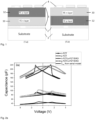
- the structures as obtained are presented in Figure 1 , configurations (1.a) and (1.b).
- Capacitance-voltage (C-V) measurements were performed at room temperature by placing the sample in a special measurement set-up with micro-manipulated arms.
- the top and bottom SRO electrodes (2, 4) were contacted with CuBe needles and the capacitance was measured at different voltages using a LRC meter from Hioki, with incorporated voltage source.
- Example of recorded C-V characteristics are presented in Figure 2a , both for the bi-layer structures of configurations (1.a) and (1.b), and for separate p-type and n-type PZT layers grown by PLD in the same conditions, on similar STO substrates, with similar SRO electrodes and thickness as the bi-layer structures.
- the p-n ferroelectric homojunction shows negative capacitance effect, the capacitance of the bi-layer structures being much larger than the capacitances of the component layers, not only in the voltage range where the polarization switching takes place (corresponding the peaks in the C-V characteristics) but on the entire voltage range used for measurements, thus for voltages for which the ferroelectric polarization is saturated. This is a steady state negative capacitance effect.
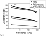
- C-f capacitance-frequency
Landscapes
- Engineering & Computer Science (AREA)
- Power Engineering (AREA)
- Manufacturing & Machinery (AREA)
- Microelectronics & Electronic Packaging (AREA)
- Ceramic Engineering (AREA)
- Chemical & Material Sciences (AREA)
- Inorganic Chemistry (AREA)
- Semiconductor Integrated Circuits (AREA)
Priority Applications (1)
| Application Number | Priority Date | Filing Date | Title |
|---|---|---|---|
| EP22465566.2A EP4369367A1 (de) | 2022-11-10 | 2022-11-10 | Kapazitive vorrichtung mit einem ferroelektrischen p-n-homoübergang mit negativer kapazität, verfahren zur herstellung davon und verwendung |
Applications Claiming Priority (1)
| Application Number | Priority Date | Filing Date | Title |
|---|---|---|---|
| EP22465566.2A EP4369367A1 (de) | 2022-11-10 | 2022-11-10 | Kapazitive vorrichtung mit einem ferroelektrischen p-n-homoübergang mit negativer kapazität, verfahren zur herstellung davon und verwendung |
Publications (1)
| Publication Number | Publication Date |
|---|---|
| EP4369367A1 true EP4369367A1 (de) | 2024-05-15 |
Family
ID=84361275
Family Applications (1)
| Application Number | Title | Priority Date | Filing Date |
|---|---|---|---|
| EP22465566.2A Pending EP4369367A1 (de) | 2022-11-10 | 2022-11-10 | Kapazitive vorrichtung mit einem ferroelektrischen p-n-homoübergang mit negativer kapazität, verfahren zur herstellung davon und verwendung |
Country Status (1)
| Country | Link |
|---|---|
| EP (1) | EP4369367A1 (de) |
Citations (3)
| Publication number | Priority date | Publication date | Assignee | Title |
|---|---|---|---|---|
| US3305394A (en) * | 1964-06-30 | 1967-02-21 | Ibm | Method of making a capacitor with a multilayered ferroelectric dielectric |
| US4772985A (en) * | 1986-09-24 | 1988-09-20 | Kabushiki Kaisha Toshiba | Thick film capacitor |
| JP2001085272A (ja) * | 1999-07-14 | 2001-03-30 | Matsushita Electric Ind Co Ltd | 可変容量コンデンサ |
-
2022
- 2022-11-10 EP EP22465566.2A patent/EP4369367A1/de active Pending
Patent Citations (3)
| Publication number | Priority date | Publication date | Assignee | Title |
|---|---|---|---|---|
| US3305394A (en) * | 1964-06-30 | 1967-02-21 | Ibm | Method of making a capacitor with a multilayered ferroelectric dielectric |
| US4772985A (en) * | 1986-09-24 | 1988-09-20 | Kabushiki Kaisha Toshiba | Thick film capacitor |
| JP2001085272A (ja) * | 1999-07-14 | 2001-03-30 | Matsushita Electric Ind Co Ltd | 可変容量コンデンサ |
Non-Patent Citations (5)
| Title |
|---|
| ASIF ISLAM KHAN: "Experimental evidence of ferroelectric negative capacitance in nanoscale heterostructures", APPL. PHYS. LETT., vol. 99, 2011, pages 113501, XP012151401, DOI: 10.1063/1.3634072 |
| ATANU K. SAHASUMEET K. GUPTA: "Negative capacitance effects in ferroelectric heterostructures: A theoretical perspective", JOURNAL OF APPLIED PHYSICS, vol. 129, 2021, pages 080901, XP012254149, DOI: 10.1063/5.0038971 |
| J MATER SCI, vol. 51, 2016, pages 499 - 505 |
| WEIWEI GAO: "Room temperature negative capacitance in a ferroelectric-dielectric superlatice heterostructure", NANO LETT, 2014 |
| WEIWEI GAO: "Room temperature negative capacitance in a ferroelectric-dielectric superlatice heterostructure", NANO LETT., 2014 |
Similar Documents
| Publication | Publication Date | Title |
|---|---|---|
| Trithaveesak et al. | Ferroelectric properties of epitaxial BaTiO3 thin films and heterostructures on different substrates | |
| Dietz et al. | Electrode influence on the charge transport through SrTiO3 thin films | |
| Roy et al. | Pulsed excimer laser ablated barium titanate thin films | |
| DE69232740T2 (de) | Spannungsvariabler kondensator | |
| Niu et al. | Molecular beam epitaxy growth of BaTiO3 thin films and crucial impact of oxygen content conditions on the electrical characteristics | |
| Pintilie et al. | Extrinsic contributions to the apparent thickness dependence of the dielectric constant in epitaxial Pb (Zr, Ti) O 3 thin films | |
| Wouters et al. | Electrical conductivity in ferroelectric thin films | |
| US20100182730A1 (en) | Ferroelectric varactor with improved tuning range | |
| Zhang et al. | Investigation of the electrical properties of RF sputtered BaTiO3 films grown on various substrates | |
| Voora et al. | Interface polarization coupling in piezoelectric-semiconductor ferroelectric heterostructures | |
| Tan et al. | Crystallographically engineered hierarchical polydomain nanostructures in perovskite ferroelectric films | |
| Pignolet et al. | Rapid thermal processed thin films of niobium pentoxide (Nb2 O5) deposited by reactive magnetron sputtering | |
| EP4369367A1 (de) | Kapazitive vorrichtung mit einem ferroelektrischen p-n-homoübergang mit negativer kapazität, verfahren zur herstellung davon und verwendung | |
| EP3154099A1 (de) | Flexoelektrische vorrichtung | |
| Stolichnov et al. | Dielectric breakdown in (Pb, La)(Zr, Ti) O 3 ferroelectric thin films with Pt and oxide electrodes | |
| Abe et al. | Nonswitching layer model for voltage shift phenomena in heteroepitaxial barium titanate thin films | |
| Nguyen et al. | Energy storage performance of silicon-integrated Sr0. 98Mn0. 02TiO3 thin film capacitors | |
| Liu et al. | Reversible metal-insulator transition in LaAlO 3 thin films mediated by intragap defects: An alternative mechanism for resistive switching | |
| Moon et al. | Formation and electrical properties of heteroepitaxial SrTiO3/SrVO3− x/Si (100) structures | |
| Tyunina et al. | Dielectric nonlinearities in ferroelectric thin-film heterostructures | |
| Kato et al. | Effect of Ozone Annealing on the Charge Trapping Property of Ta2O5–Si3N4–p-Si Capacitor Grown by Low-pressure Chemical Vapor Deposition | |
| Liu et al. | Asymmetric electrical properties in Pt/Ba0. 5Sr0. 5Ti0. 99Co0. 01O3/Nb-doped SrTiO3 capacitors | |
| Algueró et al. | The effect of film thickness on the ferroelectric properties of sol–gel prepared lanthanum modified lead titanate thin films | |
| Shirokov et al. | Polarization of thin barium-strontium titanate films by an external electric field | |
| Bharadwaja et al. | Dielectric and dc electrical studies of antiferroelectric lead zirconate thin films |
Legal Events
| Date | Code | Title | Description |
|---|---|---|---|
| PUAI | Public reference made under article 153(3) epc to a published international application that has entered the european phase |
Free format text: ORIGINAL CODE: 0009012 |
|
| STAA | Information on the status of an ep patent application or granted ep patent |
Free format text: STATUS: REQUEST FOR EXAMINATION WAS MADE |
|
| 17P | Request for examination filed |
Effective date: 20230719 |
|
| AK | Designated contracting states |
Kind code of ref document: A1 Designated state(s): AL AT BE BG CH CY CZ DE DK EE ES FI FR GB GR HR HU IE IS IT LI LT LU LV MC ME MK MT NL NO PL PT RO RS SE SI SK SM TR |