EP4369366A1 - Planares magnetisches bauteil - Google Patents
Planares magnetisches bauteil Download PDFInfo
- Publication number
- EP4369366A1 EP4369366A1 EP23209566.1A EP23209566A EP4369366A1 EP 4369366 A1 EP4369366 A1 EP 4369366A1 EP 23209566 A EP23209566 A EP 23209566A EP 4369366 A1 EP4369366 A1 EP 4369366A1
- Authority
- EP
- European Patent Office
- Prior art keywords
- trace
- hole
- current transformer
- primary
- inductor
- Prior art date
- Legal status (The legal status is an assumption and is not a legal conclusion. Google has not performed a legal analysis and makes no representation as to the accuracy of the status listed.)
- Granted
Links
Images


Classifications
-
- H—ELECTRICITY
- H02—GENERATION; CONVERSION OR DISTRIBUTION OF ELECTRIC POWER
- H02M—APPARATUS FOR CONVERSION BETWEEN AC AND AC, BETWEEN AC AND DC, OR BETWEEN DC AND DC, AND FOR USE WITH MAINS OR SIMILAR POWER SUPPLY SYSTEMS; CONVERSION OF DC OR AC INPUT POWER INTO SURGE OUTPUT POWER; CONTROL OR REGULATION THEREOF
- H02M3/00—Conversion of DC power input into DC power output
- H02M3/02—Conversion of DC power input into DC power output without intermediate conversion into AC
- H02M3/04—Conversion of DC power input into DC power output without intermediate conversion into AC by static converters
- H02M3/10—Conversion of DC power input into DC power output without intermediate conversion into AC by static converters using discharge tubes with control electrode or semiconductor devices with control electrode
- H02M3/145—Conversion of DC power input into DC power output without intermediate conversion into AC by static converters using discharge tubes with control electrode or semiconductor devices with control electrode using devices of a triode or transistor type requiring continuous application of a control signal
- H02M3/155—Conversion of DC power input into DC power output without intermediate conversion into AC by static converters using discharge tubes with control electrode or semiconductor devices with control electrode using devices of a triode or transistor type requiring continuous application of a control signal using semiconductor devices only
- H02M3/156—Conversion of DC power input into DC power output without intermediate conversion into AC by static converters using discharge tubes with control electrode or semiconductor devices with control electrode using devices of a triode or transistor type requiring continuous application of a control signal using semiconductor devices only with automatic control of output voltage or current, e.g. switching regulators
- H02M3/158—Conversion of DC power input into DC power output without intermediate conversion into AC by static converters using discharge tubes with control electrode or semiconductor devices with control electrode using devices of a triode or transistor type requiring continuous application of a control signal using semiconductor devices only with automatic control of output voltage or current, e.g. switching regulators including plural semiconductor devices as final control devices for a single load
-
- H—ELECTRICITY
- H01—ELECTRIC ELEMENTS
- H01F—MAGNETS; INDUCTANCES; TRANSFORMERS; SELECTION OF MATERIALS FOR THEIR MAGNETIC PROPERTIES
- H01F27/00—Details of transformers or inductances, in general
- H01F27/28—Coils; Windings; Conductive connections
- H01F27/2804—Printed windings
-
- H—ELECTRICITY
- H01—ELECTRIC ELEMENTS
- H01F—MAGNETS; INDUCTANCES; TRANSFORMERS; SELECTION OF MATERIALS FOR THEIR MAGNETIC PROPERTIES
- H01F27/00—Details of transformers or inductances, in general
- H01F27/24—Magnetic cores
-
- H—ELECTRICITY
- H01—ELECTRIC ELEMENTS
- H01F—MAGNETS; INDUCTANCES; TRANSFORMERS; SELECTION OF MATERIALS FOR THEIR MAGNETIC PROPERTIES
- H01F27/00—Details of transformers or inductances, in general
- H01F27/28—Coils; Windings; Conductive connections
- H01F27/29—Terminals; Tapping arrangements for signal inductances
-
- H—ELECTRICITY
- H01—ELECTRIC ELEMENTS
- H01F—MAGNETS; INDUCTANCES; TRANSFORMERS; SELECTION OF MATERIALS FOR THEIR MAGNETIC PROPERTIES
- H01F27/00—Details of transformers or inductances, in general
- H01F27/34—Special means for preventing or reducing unwanted electric or magnetic effects, e.g. no-load losses, reactive currents, harmonics, oscillations, leakage fields
- H01F27/346—Preventing or reducing leakage fields
-
- H—ELECTRICITY
- H01—ELECTRIC ELEMENTS
- H01F—MAGNETS; INDUCTANCES; TRANSFORMERS; SELECTION OF MATERIALS FOR THEIR MAGNETIC PROPERTIES
- H01F27/00—Details of transformers or inductances, in general
- H01F27/40—Structural association with built-in electric component, e.g. fuse
-
- H—ELECTRICITY
- H01—ELECTRIC ELEMENTS
- H01F—MAGNETS; INDUCTANCES; TRANSFORMERS; SELECTION OF MATERIALS FOR THEIR MAGNETIC PROPERTIES
- H01F3/00—Cores, Yokes, or armatures
- H01F3/10—Composite arrangements of magnetic circuits
- H01F3/14—Constrictions; Gaps, e.g. air-gaps
-
- H—ELECTRICITY
- H02—GENERATION; CONVERSION OR DISTRIBUTION OF ELECTRIC POWER
- H02J—CIRCUIT ARRANGEMENTS OR SYSTEMS FOR SUPPLYING OR DISTRIBUTING ELECTRIC POWER; SYSTEMS FOR STORING ELECTRIC ENERGY
- H02J1/00—Circuit arrangements for DC mains or DC distribution networks
- H02J1/08—Three-wire systems; Systems having more than three wires
- H02J1/082—Plural DC voltage, e.g. DC supply voltage with at least two different DC voltage levels
-
- H—ELECTRICITY
- H02—GENERATION; CONVERSION OR DISTRIBUTION OF ELECTRIC POWER
- H02M—APPARATUS FOR CONVERSION BETWEEN AC AND AC, BETWEEN AC AND DC, OR BETWEEN DC AND DC, AND FOR USE WITH MAINS OR SIMILAR POWER SUPPLY SYSTEMS; CONVERSION OF DC OR AC INPUT POWER INTO SURGE OUTPUT POWER; CONTROL OR REGULATION THEREOF
- H02M1/00—Details of apparatus for conversion
- H02M1/0064—Magnetic structures combining different functions, e.g. storage, filtering or transformation
-
- H—ELECTRICITY
- H02—GENERATION; CONVERSION OR DISTRIBUTION OF ELECTRIC POWER
- H02M—APPARATUS FOR CONVERSION BETWEEN AC AND AC, BETWEEN AC AND DC, OR BETWEEN DC AND DC, AND FOR USE WITH MAINS OR SIMILAR POWER SUPPLY SYSTEMS; CONVERSION OF DC OR AC INPUT POWER INTO SURGE OUTPUT POWER; CONTROL OR REGULATION THEREOF
- H02M1/00—Details of apparatus for conversion
- H02M1/42—Circuits or arrangements for compensating for or adjusting power factor in converters or inverters
- H02M1/4208—Arrangements for improving power factor of AC input
- H02M1/4225—Arrangements for improving power factor of AC input using a non-isolated boost converter
-
- H—ELECTRICITY
- H02—GENERATION; CONVERSION OR DISTRIBUTION OF ELECTRIC POWER
- H02M—APPARATUS FOR CONVERSION BETWEEN AC AND AC, BETWEEN AC AND DC, OR BETWEEN DC AND DC, AND FOR USE WITH MAINS OR SIMILAR POWER SUPPLY SYSTEMS; CONVERSION OF DC OR AC INPUT POWER INTO SURGE OUTPUT POWER; CONTROL OR REGULATION THEREOF
- H02M3/00—Conversion of DC power input into DC power output
- H02M3/003—Constructional details, e.g. physical layout, assembly, wiring or busbar connections
-
- H—ELECTRICITY
- H02—GENERATION; CONVERSION OR DISTRIBUTION OF ELECTRIC POWER
- H02M—APPARATUS FOR CONVERSION BETWEEN AC AND AC, BETWEEN AC AND DC, OR BETWEEN DC AND DC, AND FOR USE WITH MAINS OR SIMILAR POWER SUPPLY SYSTEMS; CONVERSION OF DC OR AC INPUT POWER INTO SURGE OUTPUT POWER; CONTROL OR REGULATION THEREOF
- H02M3/00—Conversion of DC power input into DC power output
- H02M3/01—Resonant DC/DC converters
-
- H—ELECTRICITY
- H02—GENERATION; CONVERSION OR DISTRIBUTION OF ELECTRIC POWER
- H02M—APPARATUS FOR CONVERSION BETWEEN AC AND AC, BETWEEN AC AND DC, OR BETWEEN DC AND DC, AND FOR USE WITH MAINS OR SIMILAR POWER SUPPLY SYSTEMS; CONVERSION OF DC OR AC INPUT POWER INTO SURGE OUTPUT POWER; CONTROL OR REGULATION THEREOF
- H02M3/00—Conversion of DC power input into DC power output
- H02M3/02—Conversion of DC power input into DC power output without intermediate conversion into AC
- H02M3/04—Conversion of DC power input into DC power output without intermediate conversion into AC by static converters
- H02M3/10—Conversion of DC power input into DC power output without intermediate conversion into AC by static converters using discharge tubes with control electrode or semiconductor devices with control electrode
- H02M3/145—Conversion of DC power input into DC power output without intermediate conversion into AC by static converters using discharge tubes with control electrode or semiconductor devices with control electrode using devices of a triode or transistor type requiring continuous application of a control signal
- H02M3/155—Conversion of DC power input into DC power output without intermediate conversion into AC by static converters using discharge tubes with control electrode or semiconductor devices with control electrode using devices of a triode or transistor type requiring continuous application of a control signal using semiconductor devices only
- H02M3/156—Conversion of DC power input into DC power output without intermediate conversion into AC by static converters using discharge tubes with control electrode or semiconductor devices with control electrode using devices of a triode or transistor type requiring continuous application of a control signal using semiconductor devices only with automatic control of output voltage or current, e.g. switching regulators
- H02M3/158—Conversion of DC power input into DC power output without intermediate conversion into AC by static converters using discharge tubes with control electrode or semiconductor devices with control electrode using devices of a triode or transistor type requiring continuous application of a control signal using semiconductor devices only with automatic control of output voltage or current, e.g. switching regulators including plural semiconductor devices as final control devices for a single load
- H02M3/1582—Buck-boost converters
-
- H—ELECTRICITY
- H02—GENERATION; CONVERSION OR DISTRIBUTION OF ELECTRIC POWER
- H02M—APPARATUS FOR CONVERSION BETWEEN AC AND AC, BETWEEN AC AND DC, OR BETWEEN DC AND DC, AND FOR USE WITH MAINS OR SIMILAR POWER SUPPLY SYSTEMS; CONVERSION OF DC OR AC INPUT POWER INTO SURGE OUTPUT POWER; CONTROL OR REGULATION THEREOF
- H02M3/00—Conversion of DC power input into DC power output
- H02M3/22—Conversion of DC power input into DC power output with intermediate conversion into AC
- H02M3/24—Conversion of DC power input into DC power output with intermediate conversion into AC by static converters
- H02M3/28—Conversion of DC power input into DC power output with intermediate conversion into AC by static converters using discharge tubes with control electrode or semiconductor devices with control electrode to produce the intermediate AC
- H02M3/325—Conversion of DC power input into DC power output with intermediate conversion into AC by static converters using discharge tubes with control electrode or semiconductor devices with control electrode to produce the intermediate AC using devices of a triode or a transistor type requiring continuous application of a control signal
- H02M3/335—Conversion of DC power input into DC power output with intermediate conversion into AC by static converters using discharge tubes with control electrode or semiconductor devices with control electrode to produce the intermediate AC using devices of a triode or a transistor type requiring continuous application of a control signal using semiconductor devices only
- H02M3/33507—Conversion of DC power input into DC power output with intermediate conversion into AC by static converters using discharge tubes with control electrode or semiconductor devices with control electrode to produce the intermediate AC using devices of a triode or a transistor type requiring continuous application of a control signal using semiconductor devices only with automatic control of the output voltage or current, e.g. flyback converters
- H02M3/33523—Conversion of DC power input into DC power output with intermediate conversion into AC by static converters using discharge tubes with control electrode or semiconductor devices with control electrode to produce the intermediate AC using devices of a triode or a transistor type requiring continuous application of a control signal using semiconductor devices only with automatic control of the output voltage or current, e.g. flyback converters with galvanic isolation between input and output of both the power stage and the feedback loop
-
- H—ELECTRICITY
- H02—GENERATION; CONVERSION OR DISTRIBUTION OF ELECTRIC POWER
- H02M—APPARATUS FOR CONVERSION BETWEEN AC AND AC, BETWEEN AC AND DC, OR BETWEEN DC AND DC, AND FOR USE WITH MAINS OR SIMILAR POWER SUPPLY SYSTEMS; CONVERSION OF DC OR AC INPUT POWER INTO SURGE OUTPUT POWER; CONTROL OR REGULATION THEREOF
- H02M7/00—Conversion of AC power input into DC power output; Conversion of DC power input into AC power output
- H02M7/02—Conversion of AC power input into DC power output without possibility of reversal
- H02M7/04—Conversion of AC power input into DC power output without possibility of reversal by static converters
- H02M7/12—Conversion of AC power input into DC power output without possibility of reversal by static converters using discharge tubes with control electrode or semiconductor devices with control electrode
- H02M7/21—Conversion of AC power input into DC power output without possibility of reversal by static converters using discharge tubes with control electrode or semiconductor devices with control electrode using devices of a triode or transistor type requiring continuous application of a control signal
- H02M7/217—Conversion of AC power input into DC power output without possibility of reversal by static converters using discharge tubes with control electrode or semiconductor devices with control electrode using devices of a triode or transistor type requiring continuous application of a control signal using semiconductor devices only
- H02M7/219—Conversion of AC power input into DC power output without possibility of reversal by static converters using discharge tubes with control electrode or semiconductor devices with control electrode using devices of a triode or transistor type requiring continuous application of a control signal using semiconductor devices only in a bridge configuration
-
- H—ELECTRICITY
- H02—GENERATION; CONVERSION OR DISTRIBUTION OF ELECTRIC POWER
- H02M—APPARATUS FOR CONVERSION BETWEEN AC AND AC, BETWEEN AC AND DC, OR BETWEEN DC AND DC, AND FOR USE WITH MAINS OR SIMILAR POWER SUPPLY SYSTEMS; CONVERSION OF DC OR AC INPUT POWER INTO SURGE OUTPUT POWER; CONTROL OR REGULATION THEREOF
- H02M7/00—Conversion of AC power input into DC power output; Conversion of DC power input into AC power output
- H02M7/02—Conversion of AC power input into DC power output without possibility of reversal
- H02M7/04—Conversion of AC power input into DC power output without possibility of reversal by static converters
- H02M7/12—Conversion of AC power input into DC power output without possibility of reversal by static converters using discharge tubes with control electrode or semiconductor devices with control electrode
- H02M7/21—Conversion of AC power input into DC power output without possibility of reversal by static converters using discharge tubes with control electrode or semiconductor devices with control electrode using devices of a triode or transistor type requiring continuous application of a control signal
- H02M7/217—Conversion of AC power input into DC power output without possibility of reversal by static converters using discharge tubes with control electrode or semiconductor devices with control electrode using devices of a triode or transistor type requiring continuous application of a control signal using semiconductor devices only
- H02M7/23—Conversion of AC power input into DC power output without possibility of reversal by static converters using discharge tubes with control electrode or semiconductor devices with control electrode using devices of a triode or transistor type requiring continuous application of a control signal using semiconductor devices only arranged for operation in parallel
-
- H—ELECTRICITY
- H05—ELECTRIC TECHNIQUES NOT OTHERWISE PROVIDED FOR
- H05K—PRINTED CIRCUITS; CASINGS OR CONSTRUCTIONAL DETAILS OF ELECTRIC APPARATUS; MANUFACTURE OF ASSEMBLAGES OF ELECTRICAL COMPONENTS
- H05K1/00—Printed circuits
- H05K1/16—Printed circuits incorporating printed electric components, e.g. printed resistor, capacitor, inductor
- H05K1/165—Printed circuits incorporating printed electric components, e.g. printed resistor, capacitor, inductor incorporating printed inductors
-
- H—ELECTRICITY
- H01—ELECTRIC ELEMENTS
- H01F—MAGNETS; INDUCTANCES; TRANSFORMERS; SELECTION OF MATERIALS FOR THEIR MAGNETIC PROPERTIES
- H01F27/00—Details of transformers or inductances, in general
- H01F27/28—Coils; Windings; Conductive connections
- H01F27/2804—Printed windings
- H01F2027/2809—Printed windings on stacked layers
-
- H—ELECTRICITY
- H01—ELECTRIC ELEMENTS
- H01F—MAGNETS; INDUCTANCES; TRANSFORMERS; SELECTION OF MATERIALS FOR THEIR MAGNETIC PROPERTIES
- H01F27/00—Details of transformers or inductances, in general
- H01F27/28—Coils; Windings; Conductive connections
- H01F27/2804—Printed windings
- H01F2027/2819—Planar transformers with printed windings, e.g. surrounded by two cores and to be mounted on printed circuit
-
- H—ELECTRICITY
- H01—ELECTRIC ELEMENTS
- H01F—MAGNETS; INDUCTANCES; TRANSFORMERS; SELECTION OF MATERIALS FOR THEIR MAGNETIC PROPERTIES
- H01F27/00—Details of transformers or inductances, in general
- H01F27/34—Special means for preventing or reducing unwanted electric or magnetic effects, e.g. no-load losses, reactive currents, harmonics, oscillations, leakage fields
- H01F2027/348—Preventing eddy currents
-
- H—ELECTRICITY
- H01—ELECTRIC ELEMENTS
- H01F—MAGNETS; INDUCTANCES; TRANSFORMERS; SELECTION OF MATERIALS FOR THEIR MAGNETIC PROPERTIES
- H01F27/00—Details of transformers or inductances, in general
- H01F27/40—Structural association with built-in electric component, e.g. fuse
- H01F2027/408—Association with diode or rectifier
-
- Y—GENERAL TAGGING OF NEW TECHNOLOGICAL DEVELOPMENTS; GENERAL TAGGING OF CROSS-SECTIONAL TECHNOLOGIES SPANNING OVER SEVERAL SECTIONS OF THE IPC; TECHNICAL SUBJECTS COVERED BY FORMER USPC CROSS-REFERENCE ART COLLECTIONS [XRACs] AND DIGESTS
- Y02—TECHNOLOGIES OR APPLICATIONS FOR MITIGATION OR ADAPTATION AGAINST CLIMATE CHANGE
- Y02B—CLIMATE CHANGE MITIGATION TECHNOLOGIES RELATED TO BUILDINGS, e.g. HOUSING, HOUSE APPLIANCES OR RELATED END-USER APPLICATIONS
- Y02B70/00—Technologies for an efficient end-user side electric power management and consumption
- Y02B70/10—Technologies improving the efficiency by using switched-mode power supplies [SMPS], i.e. efficient power electronics conversion e.g. power factor correction or reduction of losses in power supplies or efficient standby modes
Definitions
- the present disclosure relates to a planar magnetic component, and more particularly to a planar magnetic component integrated with a current transformer.
- the input voltage of information and household appliances is divided into AC voltage and DC voltage, and power supplies can generally be divided into two levels.
- the front stage is usually an AC-to-DC converter, a power factor corrector or a DC-to-DC converter
- the rear stage is usually a resonant converter.
- the resonant converter is a DC-to-DC power converter, and it has a primary-side switch that turns on at zero voltage and a secondary-side rectification switch that turns off at zero current. Therefore, it has the advantages of high power and high conversion efficiency than other converters. Furthermore, using a rectification switch on the secondary side makes it easier to achieve high efficiency and high power density.
- resonant converters usually include inductive components such as resonant inductors and transformers, and these inductive components are usually composed of coils, bobbins, and iron cores. Since the coil must be formed by winding copper wire on the winding frame for more than dozens of turns, and then the iron core is used to set the winding to form a closed magnetic circuit, resonant inductors and transformers usually have the fatal disadvantage of being bulky. Therefore, the size of the resonant converter cannot be effectively reduced, resulting in the problem of bulky power supply and poor power density.
- FIG. 1 which shows a circuit block diagram of a conventional current converter coupled to the resonant converter of the present disclosure.
- the traditional current detection is to connect a current transformer (CT) 5 in series on the primary-side path, and the current transformer 5 includes a current transformer primary-side coil 5A and a current transformer secondary-side coil 5B.
- CT current transformer
- the current transformer 5 usually requires the current transformer primary-side coil 5A and the current transformer secondary-side coil 5B to be wound around the current transformer core to detect the current, and therefore larger space and safety distance are usually required to meet the design requirements. Therefore, it is also impossible to effectively reduce the size of the resonant converter, resulting in the problem that the power supply is bulky and has poor power density.
- the planar magnetic component is arranged on a circuit board of a resonant converter, and the resonant converter includes a primary-side circuit and a secondary-side circuit.
- the planar magnetic component includes an inductor trace, an inductor iron core, and a current transformer trace.
- the inductor trace is arranged on the primary-side circuit and formed on one layer board of the circuit board to serve as a resonant inductor coupled to the primary-side circuit.
- the inductor iron core includes a core pillar, and the core pillar penetrates a through hole of the circuit board, and the inductor trace surrounds the through hole.
- the current transformer trace is formed on the circuit board to serve as a current transformer coil coupled to the resonant inductor.
- the current transformer trace surrounds the through hole to form a common-core structure that shares the inductor iron core.
- the present disclosure provides a planar magnetic component.
- the planar magnetic component is arranged on a circuit board of a resonant converter, and the resonant converter includes a primary-side circuit and a secondary-side circuit.
- the planar magnetic component includes a primary-side trace, a secondary-side trace, an iron core, and a current transformer trace.
- the primary-side trace is formed on one layer board of the circuit board to serve as a primary-side coil coupled to the primary-side circuit.
- the secondary-side trace is formed on another layer board of the circuit board to serve as a secondary-side coil coupled to the secondary-side circuit.
- the iron core includes a first core pillar and a second core pillar, and the first core pillar and the second core pillar respectively penetrate a first through hole and a second through hole of the circuit board, and the primary-side trace and the secondary-side trace surround the first through hole and the second through hole.
- the current transformer trace is formed on the circuit board to serve as a current transformer coil coupled to the secondary-side coil.
- the current transformer trace surrounds the first through hole or the second through hole to form a common-core structure that shares the iron core.
- the main purpose and effect of the present disclosure is to use the planar magnetic component in the resonant converter and integrate the current transformer coil into the planar magnetic component, so that the primary-side coil of the current transformer and the current transformer core can be omitted to reduce the contact resistance caused by the current transformer, increase efficiency, and increase power density.
- FIG. 2A shows a circuit block diagram of a resonant converter of the present disclosure, and also refer to FIG. 1 .
- the resonant converter 100 is be coupled to a front-end circuit 200 and a load 300, and the front-end circuit 200 may be a DC power supply such as an AC-to-DC converter, a power factor corrector, a DC power source, or so on.
- the resonant converter 100 includes a primary-side circuit 1A, at least one transformer 2A (two transformers are shown as an example), at least one secondary-side circuit 3A (two secondary-side circuits are shown as an example), and a controller 4A.
- the transformer 2A includes a primary-side coil 22A and a secondary-side coil 24A. Taking FIG.
- the primary-side circuit 1A is a half-bridge architecture, including one switch bridge arm SA1_M and one resonant tank (i.e., a resonant inductor Lr and a resonant capacitor Cr), and the switch bridge arm SA1_M includes two power switches Q1, Q2 connected in series.
- the secondary-side circuit 3A includes two rectification circuits 32, and each rectification circuit 32 includes two rectification switches SR1, SR2.
- the secondary-side coil 24A of the transformer 2A includes a first winding 24A-1 and a second winding 24A-2, and the first winding 24A-1 and the second winding 24A-2 are center-tapped windings.
- the resonant converter 100 can control the turning on/turning off of the rectification switches SR1, SR2 by the controller 4A, so that the first winding 24A-1 and the second winding 24A-2 are respectively coupled to the primary-side coil 22A.
- the controller 4A controls the switch bridge arm SA1_M and the rectification switches SR1, SR2 of the rectification circuit 32 to operate the resonant tank and the transformer 2A storing energy and releasing energy so as to convert the DC power source V_DC received by the resonant converter 100 into a main power source V_M.
- the circuit structures of the primary-side circuit 1A and the secondary-side circuit 3A are only illustrative examples.
- the primary-side circuit 1A (such as, but not limited to, a full-bridge structure, two resonant tanks, etc.) and the secondary-side circuit 3A (such as, but not limited to, a half-bridge rectification circuit, one rectification circuit, etc.) can form the structure of the resonant converter 100, should be included in the scope of this embodiment.
- the number of the transformers 2A is not limited to two as shown in FIG. 1 , i.e., the number of the transformer 2A may be one or more than one.
- the resonant converter 100 includes one primary-side coil 22A, one first winding 24A-1, and one second winding 24A-2, and so on.
- the resonant converter 100 further includes current transformer coils 52A, 52B.
- the current transformer primary-side coil 5A is integrated in the resonant inductor Lr and the secondary-side coil 24A, the present disclosure does not include the current transformer primary-side coil 5A.
- the current transformer coils 52A, 52B serve as the current transformer secondary-side coil 5B for sensing the current flowing through the resonant inductor Lr and the secondary-side coil 24A.
- the 2A may be coupled to, for example, but not limited to, a current detection circuit (not shown).
- the current detection circuit can generate a voltage signal according to the current sensed by the current transformer coils 52A, 52B, so as to provide the voltage signal to the controller 4A. Therefore, the controller 4A can acquire the magnitude of the current flowing through the resonant inductor Lr and the transformer 2A through calculation of the voltage signal.
- FIG. 2B shows a schematic diagram of the circuit structure of the current transformer coil coupled to a secondary-side coil of the present disclosure.
- One terminal of the current transformer coil 52B is coupled to one terminal of the first coil 24A-1 or the second coil 24A-2, and the other terminal of the current transformer coil 52B is coupled to a detection resistor Rs, and therefore the current transformer coil 52B and the detection resistor Rs are connected in parallel to the first coil 24A-1 or the second coil 24A-2.
- the secondary-side currents flowing through the rectification switches SR1, SR2 are distinguished as a first current I1 and a second current I2 respectively.
- the current transformer coil 52B When the current transformer coil 52B is coupled to the first coil 24A-1 and the first current I1 flows through the first coil 24A-1, the current transformer coil 52B induces a sensing current Ia.
- the sensing current Ia flowing through the detection resistor Rs can generate a cross-voltage Vc on the detection resistor Rs, and a back-end coupled current detection circuit (not shown) can generate a voltage signal according to the cross-voltage Vc.
- the controller 4A can realize the size of the first current I1 by calculating the cross voltage Vc.
- the current transformer coil 52B when the current transformer coil 52B is coupled to the second coil 24A-2, the operation is similar to the first coil 24A-1 and will not be described again. Since the current transformer coil 52B is only used to sense the shunt current (i.e., the sensing current Ia), its current value should not be too large. Therefore, the resistance value of the detection resistor Rs should not be too small. For example, but not limited to, a resistor with a resistance value above 10k is preferably configured. Therefore, the resistance value of the detection resistor Rs should not be too small. For example, but not limited to, a resistor with a resistance value above 10kQ is preferably configured.
- FIG. 3A shows an exploded perspective view of the resonant converter of the present disclosure, and also refer to FIG. 2A .
- the resonant converter 100 is arranged/configured on the circuit board CB1, and the switch bridge arms SA1_M, SA1_N and the controller 4A are arranged in positions as shown in FIG. 3A .
- the resonant inductor Lr and the (at least one) transformer 2A form a planar magnetic component PE.
- an inductor coil Lc of the resonant inductor Lr and the primary-side coil 22A and the secondary-side coil 24A of the transformer 2A are all planar structures, and the inductor coil Lc, the primary-side coil 22A and the secondary-side coil 24A are formed on PCB traces of the circuit board CB1.
- An iron core assembly includes an iron core C1 and an inductor iron core C_L.
- the (at least one) transformer 2A is formed by directly sleeving the iron core C1 on the primary-side coil 22A and the secondary-side coil 24A of the circuit board CB1, and the resonant inductor Lr is formed by directly sleeving the inductor iron core C _L on the inductor coil Lc of the circuit board CB1.
- the structure of the resonant converter 100 of the present disclosure mainly forms the inductor coil Lc of the resonant inductor Lr and the primary-side coil 22A and the secondary-side coil 24A of the transformer 2A on the circuit board CB1, so that the planar magnetic component PE can be planarized to significantly increase the space utilization of the resonant converter 100 and meet the requirement of the high power density.
- the planar magnetic component PE due to the small size of the planar magnetic component PE, the operating frequency of the resonant converter 100 can be significantly increased.
- the power switches of the switch bridge arms SA1_M, SA1_N and the rectification circuit 32 can use third-generation semiconductor components such as the wide bandgap (WBG) as the main power switch, so that the resonant converter 100 has the advantages of higher efficiency, significantly reduced power switch size, lighter weight, and increased heat dissipation performance.
- WBG wide bandgap
- the current transformer coils 52A, 52B of the present disclosure also have a planar structure and are formed on the circuit board CB1.
- the current transformer coil 52A is formed near the inductor coil Lc and can induce the current flowing through the inductor coil Lc through coupling, and the current transformer coil 52A reuses the common-core structure of the inductor iron core C_L shared with the inductor coil Lc to form a current transformer for sensing the primary-side current. Therefore, under the above-mentioned common core structure, the circuit volume of the resonant converter 100 can be greatly reduced, and the space utilization of the resonant converter 100 can be greatly increased to meet high power density requirements.
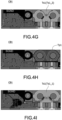
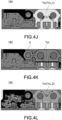
- FIG. 4A to FIG. 4L show schematic diagrams of the wiring of the coil of the planar magnetic component on each layer of the circuit board according to different embodiments of the present disclosure, and also refer to FIG. 2A to FIG. 3B .
- the circuit board CB1 is a multi-layer board (a 12-layer board is used as an example, but is not limited thereto), and FIG. 4A shows the top board, and FIG. 4L shows the bottom board.
- an inductor trace Tl serves as the inductor coil Lc
- a primary-side trace Tp1 serves as the primary-side coil 22A.
- the plurality of inductor traces Tl and the plurality of primary-side traces Tp1 are respectively formed on layer boards of FIG.
- the inductor trace T1 can be connected in series through the connection of each primary-side layer board (for example, using via holes via) to form the inductor coil Lc.
- the primary-side trace Tp1 can be connected in series through the communication of each primary-side layer board (for example, using via holes via) to serve as the primary-side coil 22A coupled to the primary-side circuit 1A.
- a plurality of secondary-side traces Ts1 serve as the secondary-side coil 24A and are formed on the layer boards of FIG. 4A, FIG. 4C , FIG. 4D, FIG. 4F , FIG.
- the secondary-side traces Ts1 can be connected in series through the connection of each secondary-side layer board (for example, using via holes via) to serve as a means for coupling the secondary-side coil 24A of the secondary-side circuit 3A.
- the iron core C1 includes a first core pillar C12 and a second core pillar C14.
- the first core pillar C12 penetrates a first through hole H1 of the circuit board CB1
- the second core pillar C14 penetrates a second through hole H2 of the circuit board CB1.
- the primary-side traces Tp1 surround the first through hole H1 and the second through hole H2
- the secondary-side traces Ts1 also surround the first through hole H1 and the second through hole H2, so that after the iron core C1 is sleeved on the primary-side traces Tp1 and the secondary-side traces Ts1, closed magnetic paths can be formed in the transformer 2A.
- the inductor iron core C_L includes a core pillar C_LC.
- the core pillar C_LC penetrates a third through hole H3 of the circuit board CB1.
- the inductor traces Tl surround the third through hole H3, so that after the inductor iron core C_L is sleeved on the inductor traces Tl, closed magnetic paths can be formed in the resonant inductor Lr.
- the material of the traces formed by each layer board may be copper foil, but it does not exclude the use of other metal foils that are easy to conduct electricity (such as, but not limited to, gold, silver, etc.).
- the primary-side traces Tp1 surround the first through hole H1 in a first direction D1 (clockwise direction/counterclockwise direction), and surround the second through hole H2 in a second direction D2 (counterclockwise direction/clockwise direction) opposite to the first direction D1 to form co-shaped traces. That is, when the primary-side traces Tp1 surround the first through hole H1 in the clockwise direction, they will surround the second through hole H2 in the counterclockwise direction. On the contrary, when the primary-side traces Tp1 surround the first through hole H1 in the counterclockwise direction, they will surround the second through hole H2 in the clockwise direction.
- the primary-side traces Tp1 shown in FIG. 4B , FIG. 4E , FIG. 4H , and FIG. 4K form two first primary-side coils 22A as shown in FIG. 3A . It can be inferred similarly that depending on the circuit configuration of the resonant converter 100, the primary-side traces Tp1 may form one or more than one first primary-side coils 22A. The number of the first primary-side coils 22A may be added depending on the number of layers of the circuit board CB1 and the number of turns of the primary-side traces Tp1, which will not be described again here.
- the primary-side traces Tp1 shown in FIG. 4B , FIG. 4E , FIG. 4H , and FIG. 4K form two primary-side coils 22A as shown in FIG. 3A . It can be inferred similarly that depending on the circuit configuration of the resonant converter 100, the primary-side traces Tp1 may form one or more than one primary-side coils 22A. The number of the primary-side coils 22A may be added depending on the number of layers of the circuit board CB1 and the number of turns of the primary-side traces Tp1, which will not be described again here.
- the primary-side traces Tp1 start from the first through hole H1 in the counterclockwise direction (i.e., the first direction D1), and approach the second through hole H2 in the clockwise direction (i.e., the second direction D2).
- the rest may be deduced by analogy, and no further details will be given.
- the first direction D1 and the second direction D2 refer to the current directions surrounding the first through hole H1 and the second through hole H2 as two different current directions, and are not limited to a clockwise direction or a counterclockwise direction. Therefore, the primary-side traces Tp 1 surround the first through-hole H1 and the second through-hole H2 for at least two turns respectively, and similarly forms an co-shaped pattern, which is referred to as an co-shaped trace.
- the primary-side traces Tp1 of the present disclosure further integrates the inductor traces Tl, and the inductor traces Tl surround the third through hole H3.
- the resonant inductor Lr is a different circuit component from the transformer 2A, in fact the two can be configured separately (that is, the two may include other circuit components, such as but not limited to, the resonant capacitor Cr), the circuit components of the two are similar in type and will also have a coil structure.
- the present disclosure it is a preferred embodiment to integrate the inductor coil Lc of the resonant inductor Lr and the primary-side coils 22A to form the planar magnetic component PE, but it is not limited to this in practice. That is, the metal foil of the inductor trace Tl of the present disclosure is directly connected to the metal foil of the primary-side trace Tp1 to form a common trace structure.
- the metal foils of the inductor trace Tl and the primary-side trace Tp1 are located on the same layer and they are an integrally formed structure, the inductor trace Tl and the primary-side trace Tp1 can also be on different layers and coupled through via holes via. Therefore, the metal foil of the inductor trace T1 can be coupled to the primary-side trace Tp1 through coupling manner to form the same path. For example, but not limited to the via holes via, or other circuit components such as the resonant capacitor Cr between the two.
- the metal foil of the inductor trace T1 and the primary-side trace Tp1 is an integrally formed structure as shown in FIG. 4B , FIG. 4E , FIG. 4H , and FIG. 4K
- the inductor trace Tl and the metal foil of the primary-side trace Tp1 can be configured separately, that is, the inductor trace Tl and the metal foil of the primary-side trace Tp1 in FIG. 4B , FIG. 4E , FIG. 4H , and FIG. 4K are disconnected, and coupled through via holes via or other circuit components that can be connected in series on this path.
- first primary-side coils 22A form two first primary-side coils 22A as shown in FIG. 2A .
- the primary-side traces Tp1 may form one or more than one primary-side coils 22A.
- the number of the first primary-side coils 22A may be added depending on the number of layers of the circuit board CB1 and the number of turns of the primary-side traces Tp1, which will not be described again here.
- the secondary-side traces Ts1 form an m-shaped trace with the first through hole H1 and the second through hole H2.
- the current flowing through the secondary-side trace Ts1 can flow out from the center point of the m-shape trace to two terminals respectively, or flow from the two terminals of the m-shape trace to the center point according to the actions of the rectification switches SR1, SR2, there will be further explanations later.
- the bottom of m-shape trace may include a plurality of via holes via.
- via holes via are filled with conductive material inside, so that the secondary-side traces Ts1 of the secondary-side layer boards in FIG. 4A, FIG. 4C , FIG. 4D, FIG. 4F , FIG. 4G, FIG. 4I , FIG. 4J, and FIG. 4L can be electrically connected to each other through the via holes via.
- the secondary-side traces Ts1 respectively include at least one first trace Ts1_1 (as shown in FIG. 4A , FIG. 4F , FIG. 4I , and FIG. 4J ) and at least one second trace Ts1_2 (as shown in FIG. 4C , FIG. 4D , FIG. 4G , and FIG. 4L ). Therefore, the number of layers of the multi-layer circuit board CB1 may be at least three or more, so that the top layer, the middle layer, and the bottom layer can separately form one first trace Ts1_1, one second trace Ts1_2, and one trace integrating the primary-side trace Tp1 with the inductor trace Tl.
- the number of the first trace Ts1_1, the second trace Ts1_2, the primary-side trace Tp1, and the inductor trace T1 can be selectively increased (based on circuit requirements).
- the secondary-side traces Ts1 of the secondary-side layer boards in FIG. 4A , FIG. 4F , FIG. 4I , and FIG. 4J can be connected through via holes via respectively to form two first coils 24A-1 (as shown in FIG. 2A ).
- the secondary-side traces Ts1 of the secondary-side layer boards in FIG. 4C , FIG. 4D , FIG. 4G , and FIG. 4L can be connected through via holes via respectively to form two second coils 24A-2 (as shown in FIG. 3A ).
- the secondary-side traces Ts1 shown in FIG. 4A, FIG. 4C , FIG. 4D, FIG. 4F , FIG. 4G, FIG. 4I , FIG. 4J, and FIG. 4L can form two first secondary-side coils 24A as shown in FIG. 1 .
- the secondary-side traces Ts1 may form one or more than one first secondary-side coils 24A.
- the number of the first secondary-side coils 24A may be added depending on the number of layers of the circuit board CB1 and the number of turns of the secondary-side traces Ts1, which will not be described again here.
- first traces Ts1_1 surround the first through hole H1 and the second through hole H2 to form an m-shaped trace.
- second traces Ts1_2 also surround the first through hole H1 and the second through hole H2 to form an m-shaped trace.
- the current direction of the first trace Ts1_1 in FIG. 4A , FIG. 4F , FIG. 4I , and FIG. 4J flows from the two terminals of the m-shaped trace to the center point, and further to the first power output terminal OUT_P1 of the circuit board CB1.
- the current direction of the second trace Ts1_2 in FIG. 4C , FIG. 4D , FIG. 4G , and FIG. 4L is exactly opposite to that of the first trace Ts1_1, that is, the current direction flows from the center point of the m-shaped trace to the two terminals, and further to the first power output terminal OUT_P1 of the circuit board CB1.
- the current transformer traces Tca, Tcb are shown in FIG. 4D , and the current transformer traces Tca, Tcb serve as current transformer coils 52A, 52B respectively.
- the current transformer trace Tca and the inductor trace Tl are arranged on different layer boards, and the current transformer trace Tca surrounds the third through hole H3 to couple the inductor trace Tl of the different layer board. Therefore, the circuit board CB1 can form a closed magnetic circuit after the inductor iron core C_L is sleeved on the inductor trace Tl and the current transformer trace Tca to constitute the resonant inductor Lr and the current transformer with a common iron core structure with the resonant inductor Lr.
- the current transformer trace Tcb and the second trace Ts1_2 are configured on the same layer board, and the current transformer trace Tcb and the second trace Ts1_2 of the secondary-side trace Ts1 have a concentric circle structure.
- the current transformer trace Tcb can also be configured on the same layer board as the first trace Ts1_1, and the current transformer trace Tcb and the second trace Ts1_2 of the secondary-side trace Ts1 have a concentric structure.
- the current transformer trace Tcb surrounds the first through hole H1 to couple the second trace Ts1_2 of the same layer board. Therefore, the circuit board CB1 can form a closed magnetic circuit to form the transformer 2A and a current transformer with a common core structure as the transformer 2A after the iron core C1 is sleeved on the primary-side trace Tp1, the secondary-side trace Ts1, and the current transformer trace Tcb. It is assumed that the current transformer trace Tcb and the first trace Ts1_1 are configured on the same layer board, and when the synchronous rectification switch SR1 is turned on, the current transformer trace Tcb can induce the first current I1 flowing through the first trace Ts1_1.
- the current transformer trace Tcb and the second trace Ts1_2 are configured on the same layer board, and when the synchronous rectification switch SR2 is turned on, the current transformer trace Tcb can induce the second current I2 flowing through the second trace Ts1_2. Since the synchronous rectification switch SR1 and the synchronous rectification switch SR2 (or diodes) are designed to be in complementary conduction (forward bias), when the synchronous rectification switch SR1 is turned on, the synchronous rectification switch SR2 is turned off, and vice versa.
- the current transformer trace Tcb is disposed closer to the first through hole H1 than the second trace Ts1_2 of the secondary-side trace Ts1, a closed magnetic circuit is formed to form the transformer 2A and a current transformer having a common core structure with the transformer 2A after the iron core C1 is sleeved on the secondary-side trace Ts1 and the current transformer trace Tcb.
- the current transformer trace Tca surrounding the third through hole H3 has a first area
- the inductor trace T1 surrounding the third through hole H3 has a second area. Since the current transformer is mainly used to sense the current flowing through the resonant inductor Lr, and the current flowing through the current transformer coil 52A is not too large, the first area must be smaller than the second area, and the area difference is preferably 1/5 to 1/10.
- the current transformer trace Tcb surrounding the first through hole H1 has a third area
- the secondary-side traces Ts1 surrounding the first through hole H1 has a fourth area. In particular, the third area must be smaller than the fourth, and the area difference is preferably 1/5 to 1/10.
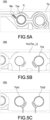
- FIG. 5A to FIG. 5C show schematic diagrams of the wiring of the coil of the planar magnetic component on each layer of the circuit board according to other different embodiments of the present disclosure, and also refer to FIG. 2A to FIG. 4L .
- the trace structures in FIG. 5A to FIG. 5C are only simple trace diagrams, so only the traces of the main components are shown, and the detailed structure can be easily inferred from the structures in FIG. 4A to FIG. 4L .
- the current transformer trace Tca and the inductor trace Tl are arranged on the same layer board, and the current transformer trace Tca is disposed closer to the third through hole H3 than the inductor trace Tl.
- the current transformer trace Tca can be coupled to the current detection circuit (not shown) through, for example, but not limited to, a via hole via.
- the current transformer trace Tcb and the first trace Ts1_1 are arranged on the same layer board, and the current transformer trace Tcb and the first trace Ts1_1 of the secondary-side trace Ts1 have a concentric structure.
- the current transformer trace Tcb surrounds the second through hole H2 to couple the first trace Ts1_1 that surrounds the second through hole H2 in the same layer board. Therefore, it is similar to FIG.
- the current transformer trace Tcb when the synchronous rectification switch SR1 is turned on, the current transformer trace Tcb can induce the first current I1 flowing through the first trace Ts1_1.
- the current transformer trace Tcb is disposed closer to the second through hole H2 than the first trace Ts1_1 of the secondary-side trace Ts1 so that a closed magnetic circuit is formed to form the transformer 2A and a current transformer having a common core structure with the transformer 2A after the iron core C1 is sleeved on the secondary-side trace Ts1 and the current transformer trace Tcb.
- the current transformer trace Tcb includes a first current transformer trace Tcb 1 and a second current transformer trace Tcb2, and the second current transformer trace Tcb2 and the first current transformer trace Tcb1 are arranged on the same layer.
- this layer independently configures the first current transformer trace Tcb1 and the second current transformer trace Tcb2 (similar to the current transformer trace Tca FIG. 4D ).
- This layer does not include any first trace Ts1_1 or second trace Ts1_2, but it does not exclude that the first current transformer trace Tcb 1 and the second current transformer trace Tcb2 may be configured on the same layer as one of the first trace Ts1_1 and the second trace Ts1_2, as long as the second current transformer trace Tcb2 and the first current transformer trace Tcb1 are configured on the same layer.
- the first current transformer trace Tcb1 surrounds the first through hole H1
- the second current transformer trace Tcb2 surrounds the second through hole H2 to couple the first trace Ts1_1 and the second trace Ts1_2 of different layer boards.
- the first current transformer trace Tcb 1 and the second current transformer trace Tcb2 can induce the first current I1 flowing through the first trace Ts1_1.
- the first current transformer trace Tcb 1 and the second current transformer trace Tcb2 can induce the second current I2 flowing through the second trace Ts1_2.
- the characteristics of the current transformer trace configuration of FIG. 4A to FIG. 5C may be applied interchangeably, and will not be described again here.
- the current transformer coils 52A, 52B have a planar structure having current transformer traces Tca, Tcb, and are respectively integrated into the inductor trace Tl and the secondary-side trace Ts1 to form the structure of the planar magnetic component PE, the current detection can be achieved by utilizing the turn ratio of the current transformer traces Tca, Tcb to the inductor trace Tl and the secondary-side trace Ts1 respectively. Therefore, the resonant converter 100 can omit the current transformer primary-side coil 5A and the current transformer core of the current transformer 5, thereby reducing the contact resistance caused by the current transformer, increasing efficiency, and increasing power density.
- the use of integrated planar magnetic component PE can increase the space utilization of the resonant converter 100 and reduce the manpower assembly in the manufacturing process.
- the primary-side coil 22A and the secondary-side coil 24A of the transformer 2A can be effectively distributed to reduce AC eddy current losses and increase efficiency.
Landscapes
- Engineering & Computer Science (AREA)
- Power Engineering (AREA)
- Chemical & Material Sciences (AREA)
- Composite Materials (AREA)
- Microelectronics & Electronic Packaging (AREA)
- Coils Or Transformers For Communication (AREA)
- Dc-Dc Converters (AREA)
- Coils Of Transformers For General Uses (AREA)
- Inverter Devices (AREA)
- Parts Printed On Printed Circuit Boards (AREA)
Applications Claiming Priority (1)
| Application Number | Priority Date | Filing Date | Title |
|---|---|---|---|
| US202263425014P | 2022-11-14 | 2022-11-14 |
Publications (2)
| Publication Number | Publication Date |
|---|---|
| EP4369366A1 true EP4369366A1 (de) | 2024-05-15 |
| EP4369366B1 EP4369366B1 (de) | 2025-04-09 |
Family
ID=88833518
Family Applications (5)
| Application Number | Title | Priority Date | Filing Date |
|---|---|---|---|
| EP23209486.2A Pending EP4369586A1 (de) | 2022-11-14 | 2023-11-13 | Stromversorgungseinheit und gleichstromumwandlungsmodul |
| EP23209566.1A Active EP4369366B1 (de) | 2022-11-14 | 2023-11-13 | Planares magnetisches bauteil |
| EP23209405.2A Pending EP4369363A3 (de) | 2022-11-14 | 2023-11-13 | Planartransformator |
| EP23209485.4A Pending EP4369364A1 (de) | 2022-11-14 | 2023-11-13 | Planares magnetisches bauteil |
| EP23209562.0A Pending EP4369365A1 (de) | 2022-11-14 | 2023-11-13 | Planartransformator |
Family Applications Before (1)
| Application Number | Title | Priority Date | Filing Date |
|---|---|---|---|
| EP23209486.2A Pending EP4369586A1 (de) | 2022-11-14 | 2023-11-13 | Stromversorgungseinheit und gleichstromumwandlungsmodul |
Family Applications After (3)
| Application Number | Title | Priority Date | Filing Date |
|---|---|---|---|
| EP23209405.2A Pending EP4369363A3 (de) | 2022-11-14 | 2023-11-13 | Planartransformator |
| EP23209485.4A Pending EP4369364A1 (de) | 2022-11-14 | 2023-11-13 | Planares magnetisches bauteil |
| EP23209562.0A Pending EP4369365A1 (de) | 2022-11-14 | 2023-11-13 | Planartransformator |
Country Status (4)
| Country | Link |
|---|---|
| US (5) | US20240161969A1 (de) |
| EP (5) | EP4369586A1 (de) |
| CN (6) | CN118039311A (de) |
| TW (7) | TW202518826A (de) |
Families Citing this family (2)
| Publication number | Priority date | Publication date | Assignee | Title |
|---|---|---|---|---|
| US20240072839A1 (en) * | 2022-08-30 | 2024-02-29 | Texas Instruments Incorporated | Differential electrical balance duplexers |
| US20250292943A1 (en) * | 2024-03-15 | 2025-09-18 | Delta Electronics, Inc. | Resonant converter |
Citations (4)
| Publication number | Priority date | Publication date | Assignee | Title |
|---|---|---|---|---|
| JP2011077328A (ja) * | 2009-09-30 | 2011-04-14 | Tdk Corp | トランス及びスイッチング電源装置 |
| US20150124489A1 (en) * | 2013-11-07 | 2015-05-07 | Futurewei Technologies, Inc. | Current Sensing Apparatus for Power Converters |
| US10516339B2 (en) * | 2016-04-06 | 2019-12-24 | Telefonaktiebolaget Lm Ericsson (Publ) | Power converter having a differential determination with secondary current sensor |
| EP3629463A1 (de) * | 2018-09-27 | 2020-04-01 | Siemens Aktiengesellschaft | Resonanter gleichspannungssteller |
Family Cites Families (22)
| Publication number | Priority date | Publication date | Assignee | Title |
|---|---|---|---|---|
| JP2002299130A (ja) * | 2001-04-02 | 2002-10-11 | Densei Lambda Kk | 電源用複合素子 |
| CN101917053B (zh) * | 2010-08-03 | 2012-10-24 | 浪潮电子信息产业股份有限公司 | 一种对rack系统集中式供电的方法 |
| CN105655113B (zh) * | 2014-11-12 | 2018-04-17 | 台达电子工业股份有限公司 | Pcb平面变压器及使用这种变压器的变换器 |
| CN106484045B (zh) * | 2015-08-25 | 2020-06-30 | 佛山市顺德区顺达电脑厂有限公司 | 服务器 |
| TWI542135B (zh) * | 2015-09-11 | 2016-07-11 | 萬國半導體(開曼)股份有限公司 | 電壓轉換器 |
| US10348119B2 (en) * | 2016-02-05 | 2019-07-09 | Guangdong Oppo Mobile Telecommunications Corp., Ltd. | Adapter and method for charging control |
| CN106655721A (zh) * | 2017-03-13 | 2017-05-10 | 杭州富特科技股份有限公司 | 一种电源功率模块及其电路板组合及一种功率转换器 |
| CN107818865B (zh) * | 2017-09-19 | 2019-05-31 | 东南大学 | 一种半桥llc谐振变换器中的高频中间抽头平面变压器 |
| TWI630628B (zh) * | 2017-10-19 | 2018-07-21 | 光壽科技有限公司 | Capacitive resistance voltage conversion device |
| CN109494749B (zh) * | 2018-11-30 | 2021-03-26 | 华中科技大学 | 一种即插即用集成模块化串联型动态电压补偿器 |
| CN111383830B (zh) * | 2018-12-29 | 2021-05-28 | 台达电子企业管理(上海)有限公司 | 磁性单元 |
| CN109546872B (zh) * | 2019-01-22 | 2023-09-15 | 东莞育嘉电子有限公司 | 并联叠加可无限扩充的电源系统 |
| US11848140B2 (en) * | 2019-06-11 | 2023-12-19 | Virginia Tech Intellectual Properties, Inc. | Integrated parallel matrix transformer and inductor |
| CN112564485B (zh) * | 2019-09-10 | 2022-03-08 | 中车株洲电力机车研究所有限公司 | Llc谐振变换器及其控制方法 |
| CN111463879A (zh) * | 2020-04-29 | 2020-07-28 | 恩益达电源科技(苏州)有限公司 | 一种用于充电桩的功率控制系统 |
| DE102020118708A1 (de) * | 2020-07-15 | 2022-01-20 | WAGO Verwaltungsgesellschaft mit beschränkter Haftung | Elektrische anordnung mit übertrager zum übertragen von signalen von einer primärseite zu einer sekundärseite |
| AU2021313127A1 (en) * | 2020-07-21 | 2023-03-09 | Omnifi Inc. | Flexible wireless interconnection and board diversity |
| US11594973B2 (en) * | 2020-08-04 | 2023-02-28 | Delta Electronics Inc. | Multiple-port bidirectional converter and control method thereof |
| TWM612250U (zh) * | 2021-01-14 | 2021-05-21 | 台達電子工業股份有限公司 | 磁性元件 |
| US20230162905A1 (en) * | 2021-02-08 | 2023-05-25 | Navitas Semiconductor Limited | Planar transformer including noise cancellation for auxiliary winding |
| US20230005659A1 (en) * | 2021-07-05 | 2023-01-05 | Navitas Semiconductor Limited | Systems and methods for improving winding losses in planar transformers |
| CN116076011B (zh) * | 2022-10-12 | 2025-10-28 | 英诺赛科(深圳)半导体有限公司 | 具有平面变压器的基于GaN的开关模式电力供应器 |
-
2023
- 2023-11-13 EP EP23209486.2A patent/EP4369586A1/de active Pending
- 2023-11-13 TW TW114100115A patent/TW202518826A/zh unknown
- 2023-11-13 US US18/507,775 patent/US20240161969A1/en active Pending
- 2023-11-13 TW TW112143628A patent/TWI872803B/zh active
- 2023-11-13 US US18/507,853 patent/US20240162833A1/en active Pending
- 2023-11-13 TW TW112212259U patent/TWM656161U/zh unknown
- 2023-11-13 TW TW112143654A patent/TWI852831B/zh active
- 2023-11-13 US US18/507,694 patent/US20240161967A1/en active Pending
- 2023-11-13 CN CN202311504360.0A patent/CN118039311A/zh active Pending
- 2023-11-13 US US18/507,751 patent/US20240161968A1/en active Pending
- 2023-11-13 CN CN202311504365.3A patent/CN118041064A/zh active Pending
- 2023-11-13 EP EP23209566.1A patent/EP4369366B1/de active Active
- 2023-11-13 CN CN202323055274.4U patent/CN221551625U/zh active Active
- 2023-11-13 EP EP23209405.2A patent/EP4369363A3/de active Pending
- 2023-11-13 EP EP23209485.4A patent/EP4369364A1/de active Pending
- 2023-11-13 EP EP23209562.0A patent/EP4369365A1/de active Pending
- 2023-11-13 CN CN202311504362.XA patent/CN118039312A/zh active Pending
- 2023-11-13 CN CN202311504363.4A patent/CN118039313A/zh active Pending
- 2023-11-13 TW TW112143629A patent/TWI890192B/zh active
- 2023-11-13 TW TW112143653A patent/TWI891121B/zh active
- 2023-11-13 CN CN202311506112.XA patent/CN118039314A/zh active Pending
- 2023-11-13 US US18/507,446 patent/US20240161966A1/en active Pending
- 2023-11-13 TW TW112143640A patent/TWI879226B/zh active
Patent Citations (4)
| Publication number | Priority date | Publication date | Assignee | Title |
|---|---|---|---|---|
| JP2011077328A (ja) * | 2009-09-30 | 2011-04-14 | Tdk Corp | トランス及びスイッチング電源装置 |
| US20150124489A1 (en) * | 2013-11-07 | 2015-05-07 | Futurewei Technologies, Inc. | Current Sensing Apparatus for Power Converters |
| US10516339B2 (en) * | 2016-04-06 | 2019-12-24 | Telefonaktiebolaget Lm Ericsson (Publ) | Power converter having a differential determination with secondary current sensor |
| EP3629463A1 (de) * | 2018-09-27 | 2020-04-01 | Siemens Aktiengesellschaft | Resonanter gleichspannungssteller |
Also Published As
| Publication number | Publication date |
|---|---|
| CN118041064A (zh) | 2024-05-14 |
| US20240161967A1 (en) | 2024-05-16 |
| CN118039312A (zh) | 2024-05-14 |
| EP4369366B1 (de) | 2025-04-09 |
| EP4369365A1 (de) | 2024-05-15 |
| US20240162833A1 (en) | 2024-05-16 |
| US20240161968A1 (en) | 2024-05-16 |
| TWI852831B (zh) | 2024-08-11 |
| TW202429494A (zh) | 2024-07-16 |
| TWI879226B (zh) | 2025-04-01 |
| EP4369586A1 (de) | 2024-05-15 |
| CN221551625U (zh) | 2024-08-16 |
| US20240161969A1 (en) | 2024-05-16 |
| TW202427508A (zh) | 2024-07-01 |
| EP4369363A3 (de) | 2024-07-10 |
| TWI872803B (zh) | 2025-02-11 |
| CN118039314A (zh) | 2024-05-14 |
| TW202420345A (zh) | 2024-05-16 |
| TWI890192B (zh) | 2025-07-11 |
| TW202420346A (zh) | 2024-05-16 |
| TW202518826A (zh) | 2025-05-01 |
| TWM656161U (zh) | 2024-06-01 |
| CN118039313A (zh) | 2024-05-14 |
| EP4369363A2 (de) | 2024-05-15 |
| CN118039311A (zh) | 2024-05-14 |
| US20240161966A1 (en) | 2024-05-16 |
| TWI891121B (zh) | 2025-07-21 |
| TW202420723A (zh) | 2024-05-16 |
| EP4369364A1 (de) | 2024-05-15 |
Similar Documents
| Publication | Publication Date | Title |
|---|---|---|
| EP4369366A1 (de) | Planares magnetisches bauteil | |
| US11587718B2 (en) | Integrated transformer and power converter | |
| US11791087B2 (en) | Planar converter | |
| CN206421898U (zh) | 带有抽头的pcb平板变压器 | |
| JP2004112991A (ja) | スイッチング電源装置 | |
| TWI905041B (zh) | 諧振轉換器 | |
| US20250293595A1 (en) | Resonant converter | |
| TWI905043B (zh) | 諧振轉換器 | |
| EP4583131A1 (de) | Transformator und llc-resonanzwandler damit | |
| JP7120154B2 (ja) | 変成器 | |
| TW202539155A (zh) | 諧振轉換器 | |
| TW202539153A (zh) | 諧振轉換器 |
Legal Events
| Date | Code | Title | Description |
|---|---|---|---|
| PUAI | Public reference made under article 153(3) epc to a published international application that has entered the european phase |
Free format text: ORIGINAL CODE: 0009012 |
|
| STAA | Information on the status of an ep patent application or granted ep patent |
Free format text: STATUS: THE APPLICATION HAS BEEN PUBLISHED |
|
| AK | Designated contracting states |
Kind code of ref document: A1 Designated state(s): AL AT BE BG CH CY CZ DE DK EE ES FI FR GB GR HR HU IE IS IT LI LT LU LV MC ME MK MT NL NO PL PT RO RS SE SI SK SM TR |
|
| STAA | Information on the status of an ep patent application or granted ep patent |
Free format text: STATUS: REQUEST FOR EXAMINATION WAS MADE |
|
| 17P | Request for examination filed |
Effective date: 20240928 |
|
| RBV | Designated contracting states (corrected) |
Designated state(s): AL AT BE BG CH CY CZ DE DK EE ES FI FR GB GR HR HU IE IS IT LI LT LU LV MC ME MK MT NL NO PL PT RO RS SE SI SK SM TR |
|
| GRAP | Despatch of communication of intention to grant a patent |
Free format text: ORIGINAL CODE: EPIDOSNIGR1 |
|
| STAA | Information on the status of an ep patent application or granted ep patent |
Free format text: STATUS: GRANT OF PATENT IS INTENDED |
|
| INTG | Intention to grant announced |
Effective date: 20241118 |
|
| RAP3 | Party data changed (applicant data changed or rights of an application transferred) |
Owner name: DELTA ELECTRONICS, INC. |
|
| RIN1 | Information on inventor provided before grant (corrected) |
Inventor name: CHU, CHIA-WEI Inventor name: LAI, CHIEN-AN Inventor name: CHANG, YI-SHENG Inventor name: CHIU, YI-HSUN |
|
| GRAS | Grant fee paid |
Free format text: ORIGINAL CODE: EPIDOSNIGR3 |
|
| P01 | Opt-out of the competence of the unified patent court (upc) registered |
Free format text: CASE NUMBER: APP_4740/2025 Effective date: 20250128 |
|
| GRAA | (expected) grant |
Free format text: ORIGINAL CODE: 0009210 |
|
| STAA | Information on the status of an ep patent application or granted ep patent |
Free format text: STATUS: THE PATENT HAS BEEN GRANTED |
|
| AK | Designated contracting states |
Kind code of ref document: B1 Designated state(s): AL AT BE BG CH CY CZ DE DK EE ES FI FR GB GR HR HU IE IS IT LI LT LU LV MC ME MK MT NL NO PL PT RO RS SE SI SK SM TR |
|
| REG | Reference to a national code |
Ref country code: GB Ref legal event code: FG4D |
|
| REG | Reference to a national code |
Ref country code: CH Ref legal event code: EP |
|
| REG | Reference to a national code |
Ref country code: DE Ref legal event code: R096 Ref document number: 602023002837 Country of ref document: DE |
|
| REG | Reference to a national code |
Ref country code: IE Ref legal event code: FG4D |
|
| REG | Reference to a national code |
Ref country code: NL Ref legal event code: MP Effective date: 20250409 |
|
| PG25 | Lapsed in a contracting state [announced via postgrant information from national office to epo] |
Ref country code: NL Free format text: LAPSE BECAUSE OF FAILURE TO SUBMIT A TRANSLATION OF THE DESCRIPTION OR TO PAY THE FEE WITHIN THE PRESCRIBED TIME-LIMIT Effective date: 20250409 |
|
| REG | Reference to a national code |
Ref country code: AT Ref legal event code: MK05 Ref document number: 1784339 Country of ref document: AT Kind code of ref document: T Effective date: 20250409 |
|
| PG25 | Lapsed in a contracting state [announced via postgrant information from national office to epo] |
Ref country code: FI Free format text: LAPSE BECAUSE OF FAILURE TO SUBMIT A TRANSLATION OF THE DESCRIPTION OR TO PAY THE FEE WITHIN THE PRESCRIBED TIME-LIMIT Effective date: 20250409 Ref country code: PT Free format text: LAPSE BECAUSE OF FAILURE TO SUBMIT A TRANSLATION OF THE DESCRIPTION OR TO PAY THE FEE WITHIN THE PRESCRIBED TIME-LIMIT Effective date: 20250811 Ref country code: ES Free format text: LAPSE BECAUSE OF FAILURE TO SUBMIT A TRANSLATION OF THE DESCRIPTION OR TO PAY THE FEE WITHIN THE PRESCRIBED TIME-LIMIT Effective date: 20250409 |
|
| REG | Reference to a national code |
Ref country code: LT Ref legal event code: MG9D |
|
| PG25 | Lapsed in a contracting state [announced via postgrant information from national office to epo] |
Ref country code: NO Free format text: LAPSE BECAUSE OF FAILURE TO SUBMIT A TRANSLATION OF THE DESCRIPTION OR TO PAY THE FEE WITHIN THE PRESCRIBED TIME-LIMIT Effective date: 20250709 Ref country code: GR Free format text: LAPSE BECAUSE OF FAILURE TO SUBMIT A TRANSLATION OF THE DESCRIPTION OR TO PAY THE FEE WITHIN THE PRESCRIBED TIME-LIMIT Effective date: 20250710 |
|
| PG25 | Lapsed in a contracting state [announced via postgrant information from national office to epo] |
Ref country code: PL Free format text: LAPSE BECAUSE OF FAILURE TO SUBMIT A TRANSLATION OF THE DESCRIPTION OR TO PAY THE FEE WITHIN THE PRESCRIBED TIME-LIMIT Effective date: 20250409 |
|
| PG25 | Lapsed in a contracting state [announced via postgrant information from national office to epo] |
Ref country code: BG Free format text: LAPSE BECAUSE OF FAILURE TO SUBMIT A TRANSLATION OF THE DESCRIPTION OR TO PAY THE FEE WITHIN THE PRESCRIBED TIME-LIMIT Effective date: 20250409 |
|
| PG25 | Lapsed in a contracting state [announced via postgrant information from national office to epo] |
Ref country code: HR Free format text: LAPSE BECAUSE OF FAILURE TO SUBMIT A TRANSLATION OF THE DESCRIPTION OR TO PAY THE FEE WITHIN THE PRESCRIBED TIME-LIMIT Effective date: 20250409 |
|
| PG25 | Lapsed in a contracting state [announced via postgrant information from national office to epo] |
Ref country code: AT Free format text: LAPSE BECAUSE OF FAILURE TO SUBMIT A TRANSLATION OF THE DESCRIPTION OR TO PAY THE FEE WITHIN THE PRESCRIBED TIME-LIMIT Effective date: 20250409 |
|
| PG25 | Lapsed in a contracting state [announced via postgrant information from national office to epo] |
Ref country code: RS Free format text: LAPSE BECAUSE OF FAILURE TO SUBMIT A TRANSLATION OF THE DESCRIPTION OR TO PAY THE FEE WITHIN THE PRESCRIBED TIME-LIMIT Effective date: 20250709 |
|
| PG25 | Lapsed in a contracting state [announced via postgrant information from national office to epo] |
Ref country code: IS Free format text: LAPSE BECAUSE OF FAILURE TO SUBMIT A TRANSLATION OF THE DESCRIPTION OR TO PAY THE FEE WITHIN THE PRESCRIBED TIME-LIMIT Effective date: 20250809 |
|
| PG25 | Lapsed in a contracting state [announced via postgrant information from national office to epo] |
Ref country code: LV Free format text: LAPSE BECAUSE OF FAILURE TO SUBMIT A TRANSLATION OF THE DESCRIPTION OR TO PAY THE FEE WITHIN THE PRESCRIBED TIME-LIMIT Effective date: 20250409 |