EP4369363A2 - Planar transformer - Google Patents
Planar transformer Download PDFInfo
- Publication number
- EP4369363A2 EP4369363A2 EP23209405.2A EP23209405A EP4369363A2 EP 4369363 A2 EP4369363 A2 EP 4369363A2 EP 23209405 A EP23209405 A EP 23209405A EP 4369363 A2 EP4369363 A2 EP 4369363A2
- Authority
- EP
- European Patent Office
- Prior art keywords
- primary
- trace
- circuit board
- circuit
- layer
- Prior art date
- Legal status (The legal status is an assumption and is not a legal conclusion. Google has not performed a legal analysis and makes no representation as to the accuracy of the status listed.)
- Pending
Links
Images


Classifications
-
- H—ELECTRICITY
- H02—GENERATION; CONVERSION OR DISTRIBUTION OF ELECTRIC POWER
- H02M—APPARATUS FOR CONVERSION BETWEEN AC AND AC, BETWEEN AC AND DC, OR BETWEEN DC AND DC, AND FOR USE WITH MAINS OR SIMILAR POWER SUPPLY SYSTEMS; CONVERSION OF DC OR AC INPUT POWER INTO SURGE OUTPUT POWER; CONTROL OR REGULATION THEREOF
- H02M3/00—Conversion of DC power input into DC power output
- H02M3/02—Conversion of DC power input into DC power output without intermediate conversion into AC
- H02M3/04—Conversion of DC power input into DC power output without intermediate conversion into AC by static converters
- H02M3/10—Conversion of DC power input into DC power output without intermediate conversion into AC by static converters using discharge tubes with control electrode or semiconductor devices with control electrode
- H02M3/145—Conversion of DC power input into DC power output without intermediate conversion into AC by static converters using discharge tubes with control electrode or semiconductor devices with control electrode using devices of a triode or transistor type requiring continuous application of a control signal
- H02M3/155—Conversion of DC power input into DC power output without intermediate conversion into AC by static converters using discharge tubes with control electrode or semiconductor devices with control electrode using devices of a triode or transistor type requiring continuous application of a control signal using semiconductor devices only
- H02M3/156—Conversion of DC power input into DC power output without intermediate conversion into AC by static converters using discharge tubes with control electrode or semiconductor devices with control electrode using devices of a triode or transistor type requiring continuous application of a control signal using semiconductor devices only with automatic control of output voltage or current, e.g. switching regulators
- H02M3/158—Conversion of DC power input into DC power output without intermediate conversion into AC by static converters using discharge tubes with control electrode or semiconductor devices with control electrode using devices of a triode or transistor type requiring continuous application of a control signal using semiconductor devices only with automatic control of output voltage or current, e.g. switching regulators including plural semiconductor devices as final control devices for a single load
-
- H—ELECTRICITY
- H01—ELECTRIC ELEMENTS
- H01F—MAGNETS; INDUCTANCES; TRANSFORMERS; SELECTION OF MATERIALS FOR THEIR MAGNETIC PROPERTIES
- H01F27/00—Details of transformers or inductances, in general
- H01F27/28—Coils; Windings; Conductive connections
- H01F27/2804—Printed windings
-
- H—ELECTRICITY
- H01—ELECTRIC ELEMENTS
- H01F—MAGNETS; INDUCTANCES; TRANSFORMERS; SELECTION OF MATERIALS FOR THEIR MAGNETIC PROPERTIES
- H01F27/00—Details of transformers or inductances, in general
- H01F27/24—Magnetic cores
-
- H—ELECTRICITY
- H01—ELECTRIC ELEMENTS
- H01F—MAGNETS; INDUCTANCES; TRANSFORMERS; SELECTION OF MATERIALS FOR THEIR MAGNETIC PROPERTIES
- H01F27/00—Details of transformers or inductances, in general
- H01F27/28—Coils; Windings; Conductive connections
- H01F27/29—Terminals; Tapping arrangements for signal inductances
-
- H—ELECTRICITY
- H01—ELECTRIC ELEMENTS
- H01F—MAGNETS; INDUCTANCES; TRANSFORMERS; SELECTION OF MATERIALS FOR THEIR MAGNETIC PROPERTIES
- H01F27/00—Details of transformers or inductances, in general
- H01F27/34—Special means for preventing or reducing unwanted electric or magnetic effects, e.g. no-load losses, reactive currents, harmonics, oscillations, leakage fields
- H01F27/346—Preventing or reducing leakage fields
-
- H—ELECTRICITY
- H01—ELECTRIC ELEMENTS
- H01F—MAGNETS; INDUCTANCES; TRANSFORMERS; SELECTION OF MATERIALS FOR THEIR MAGNETIC PROPERTIES
- H01F27/00—Details of transformers or inductances, in general
- H01F27/40—Structural association with built-in electric component, e.g. fuse
-
- H—ELECTRICITY
- H01—ELECTRIC ELEMENTS
- H01F—MAGNETS; INDUCTANCES; TRANSFORMERS; SELECTION OF MATERIALS FOR THEIR MAGNETIC PROPERTIES
- H01F3/00—Cores, Yokes, or armatures
- H01F3/10—Composite arrangements of magnetic circuits
- H01F3/14—Constrictions; Gaps, e.g. air-gaps
-
- H—ELECTRICITY
- H02—GENERATION; CONVERSION OR DISTRIBUTION OF ELECTRIC POWER
- H02J—ELECTRIC POWER NETWORKS; CIRCUIT ARRANGEMENTS OR SYSTEMS FOR SUPPLYING OR DISTRIBUTING ELECTRIC POWER; SYSTEMS FOR STORING ELECTRIC ENERGY
- H02J1/00—Circuit arrangements for DC mains or DC distribution networks
- H02J1/08—Three-wire DC power distribution systems; Systems having more than three wires
- H02J1/082—DC supplies with two or more different DC voltage levels
-
- H—ELECTRICITY
- H02—GENERATION; CONVERSION OR DISTRIBUTION OF ELECTRIC POWER
- H02M—APPARATUS FOR CONVERSION BETWEEN AC AND AC, BETWEEN AC AND DC, OR BETWEEN DC AND DC, AND FOR USE WITH MAINS OR SIMILAR POWER SUPPLY SYSTEMS; CONVERSION OF DC OR AC INPUT POWER INTO SURGE OUTPUT POWER; CONTROL OR REGULATION THEREOF
- H02M1/00—Details of apparatus for conversion
- H02M1/0064—Magnetic structures combining different functions, e.g. storage, filtering or transformation
-
- H—ELECTRICITY
- H02—GENERATION; CONVERSION OR DISTRIBUTION OF ELECTRIC POWER
- H02M—APPARATUS FOR CONVERSION BETWEEN AC AND AC, BETWEEN AC AND DC, OR BETWEEN DC AND DC, AND FOR USE WITH MAINS OR SIMILAR POWER SUPPLY SYSTEMS; CONVERSION OF DC OR AC INPUT POWER INTO SURGE OUTPUT POWER; CONTROL OR REGULATION THEREOF
- H02M1/00—Details of apparatus for conversion
- H02M1/42—Circuits or arrangements for compensating for or adjusting power factor in converters or inverters
- H02M1/4208—Arrangements for improving power factor of AC input
- H02M1/4225—Arrangements for improving power factor of AC input using a non-isolated boost converter
-
- H—ELECTRICITY
- H02—GENERATION; CONVERSION OR DISTRIBUTION OF ELECTRIC POWER
- H02M—APPARATUS FOR CONVERSION BETWEEN AC AND AC, BETWEEN AC AND DC, OR BETWEEN DC AND DC, AND FOR USE WITH MAINS OR SIMILAR POWER SUPPLY SYSTEMS; CONVERSION OF DC OR AC INPUT POWER INTO SURGE OUTPUT POWER; CONTROL OR REGULATION THEREOF
- H02M3/00—Conversion of DC power input into DC power output
- H02M3/003—Constructional details, e.g. physical layout, assembly, wiring or busbar connections
-
- H—ELECTRICITY
- H02—GENERATION; CONVERSION OR DISTRIBUTION OF ELECTRIC POWER
- H02M—APPARATUS FOR CONVERSION BETWEEN AC AND AC, BETWEEN AC AND DC, OR BETWEEN DC AND DC, AND FOR USE WITH MAINS OR SIMILAR POWER SUPPLY SYSTEMS; CONVERSION OF DC OR AC INPUT POWER INTO SURGE OUTPUT POWER; CONTROL OR REGULATION THEREOF
- H02M3/00—Conversion of DC power input into DC power output
- H02M3/01—Resonant DC/DC converters
-
- H—ELECTRICITY
- H02—GENERATION; CONVERSION OR DISTRIBUTION OF ELECTRIC POWER
- H02M—APPARATUS FOR CONVERSION BETWEEN AC AND AC, BETWEEN AC AND DC, OR BETWEEN DC AND DC, AND FOR USE WITH MAINS OR SIMILAR POWER SUPPLY SYSTEMS; CONVERSION OF DC OR AC INPUT POWER INTO SURGE OUTPUT POWER; CONTROL OR REGULATION THEREOF
- H02M3/00—Conversion of DC power input into DC power output
- H02M3/02—Conversion of DC power input into DC power output without intermediate conversion into AC
- H02M3/04—Conversion of DC power input into DC power output without intermediate conversion into AC by static converters
- H02M3/10—Conversion of DC power input into DC power output without intermediate conversion into AC by static converters using discharge tubes with control electrode or semiconductor devices with control electrode
- H02M3/145—Conversion of DC power input into DC power output without intermediate conversion into AC by static converters using discharge tubes with control electrode or semiconductor devices with control electrode using devices of a triode or transistor type requiring continuous application of a control signal
- H02M3/155—Conversion of DC power input into DC power output without intermediate conversion into AC by static converters using discharge tubes with control electrode or semiconductor devices with control electrode using devices of a triode or transistor type requiring continuous application of a control signal using semiconductor devices only
- H02M3/156—Conversion of DC power input into DC power output without intermediate conversion into AC by static converters using discharge tubes with control electrode or semiconductor devices with control electrode using devices of a triode or transistor type requiring continuous application of a control signal using semiconductor devices only with automatic control of output voltage or current, e.g. switching regulators
- H02M3/158—Conversion of DC power input into DC power output without intermediate conversion into AC by static converters using discharge tubes with control electrode or semiconductor devices with control electrode using devices of a triode or transistor type requiring continuous application of a control signal using semiconductor devices only with automatic control of output voltage or current, e.g. switching regulators including plural semiconductor devices as final control devices for a single load
- H02M3/1582—Buck-boost converters
-
- H—ELECTRICITY
- H02—GENERATION; CONVERSION OR DISTRIBUTION OF ELECTRIC POWER
- H02M—APPARATUS FOR CONVERSION BETWEEN AC AND AC, BETWEEN AC AND DC, OR BETWEEN DC AND DC, AND FOR USE WITH MAINS OR SIMILAR POWER SUPPLY SYSTEMS; CONVERSION OF DC OR AC INPUT POWER INTO SURGE OUTPUT POWER; CONTROL OR REGULATION THEREOF
- H02M3/00—Conversion of DC power input into DC power output
- H02M3/22—Conversion of DC power input into DC power output with intermediate conversion into AC
- H02M3/24—Conversion of DC power input into DC power output with intermediate conversion into AC by static converters
- H02M3/28—Conversion of DC power input into DC power output with intermediate conversion into AC by static converters using discharge tubes with control electrode or semiconductor devices with control electrode to produce the intermediate AC
- H02M3/325—Conversion of DC power input into DC power output with intermediate conversion into AC by static converters using discharge tubes with control electrode or semiconductor devices with control electrode to produce the intermediate AC using devices of a triode or a transistor type requiring continuous application of a control signal
- H02M3/335—Conversion of DC power input into DC power output with intermediate conversion into AC by static converters using discharge tubes with control electrode or semiconductor devices with control electrode to produce the intermediate AC using devices of a triode or a transistor type requiring continuous application of a control signal using semiconductor devices only
-
- H—ELECTRICITY
- H02—GENERATION; CONVERSION OR DISTRIBUTION OF ELECTRIC POWER
- H02M—APPARATUS FOR CONVERSION BETWEEN AC AND AC, BETWEEN AC AND DC, OR BETWEEN DC AND DC, AND FOR USE WITH MAINS OR SIMILAR POWER SUPPLY SYSTEMS; CONVERSION OF DC OR AC INPUT POWER INTO SURGE OUTPUT POWER; CONTROL OR REGULATION THEREOF
- H02M3/00—Conversion of DC power input into DC power output
- H02M3/22—Conversion of DC power input into DC power output with intermediate conversion into AC
- H02M3/24—Conversion of DC power input into DC power output with intermediate conversion into AC by static converters
- H02M3/28—Conversion of DC power input into DC power output with intermediate conversion into AC by static converters using discharge tubes with control electrode or semiconductor devices with control electrode to produce the intermediate AC
- H02M3/325—Conversion of DC power input into DC power output with intermediate conversion into AC by static converters using discharge tubes with control electrode or semiconductor devices with control electrode to produce the intermediate AC using devices of a triode or a transistor type requiring continuous application of a control signal
- H02M3/335—Conversion of DC power input into DC power output with intermediate conversion into AC by static converters using discharge tubes with control electrode or semiconductor devices with control electrode to produce the intermediate AC using devices of a triode or a transistor type requiring continuous application of a control signal using semiconductor devices only
- H02M3/33507—Conversion of DC power input into DC power output with intermediate conversion into AC by static converters using discharge tubes with control electrode or semiconductor devices with control electrode to produce the intermediate AC using devices of a triode or a transistor type requiring continuous application of a control signal using semiconductor devices only with automatic control of the output voltage or current, e.g. flyback converters
-
- H—ELECTRICITY
- H02—GENERATION; CONVERSION OR DISTRIBUTION OF ELECTRIC POWER
- H02M—APPARATUS FOR CONVERSION BETWEEN AC AND AC, BETWEEN AC AND DC, OR BETWEEN DC AND DC, AND FOR USE WITH MAINS OR SIMILAR POWER SUPPLY SYSTEMS; CONVERSION OF DC OR AC INPUT POWER INTO SURGE OUTPUT POWER; CONTROL OR REGULATION THEREOF
- H02M3/00—Conversion of DC power input into DC power output
- H02M3/22—Conversion of DC power input into DC power output with intermediate conversion into AC
- H02M3/24—Conversion of DC power input into DC power output with intermediate conversion into AC by static converters
- H02M3/28—Conversion of DC power input into DC power output with intermediate conversion into AC by static converters using discharge tubes with control electrode or semiconductor devices with control electrode to produce the intermediate AC
- H02M3/325—Conversion of DC power input into DC power output with intermediate conversion into AC by static converters using discharge tubes with control electrode or semiconductor devices with control electrode to produce the intermediate AC using devices of a triode or a transistor type requiring continuous application of a control signal
- H02M3/335—Conversion of DC power input into DC power output with intermediate conversion into AC by static converters using discharge tubes with control electrode or semiconductor devices with control electrode to produce the intermediate AC using devices of a triode or a transistor type requiring continuous application of a control signal using semiconductor devices only
- H02M3/33507—Conversion of DC power input into DC power output with intermediate conversion into AC by static converters using discharge tubes with control electrode or semiconductor devices with control electrode to produce the intermediate AC using devices of a triode or a transistor type requiring continuous application of a control signal using semiconductor devices only with automatic control of the output voltage or current, e.g. flyback converters
- H02M3/33523—Conversion of DC power input into DC power output with intermediate conversion into AC by static converters using discharge tubes with control electrode or semiconductor devices with control electrode to produce the intermediate AC using devices of a triode or a transistor type requiring continuous application of a control signal using semiconductor devices only with automatic control of the output voltage or current, e.g. flyback converters with galvanic isolation between input and output of both the power stage and the feedback loop
-
- H—ELECTRICITY
- H02—GENERATION; CONVERSION OR DISTRIBUTION OF ELECTRIC POWER
- H02M—APPARATUS FOR CONVERSION BETWEEN AC AND AC, BETWEEN AC AND DC, OR BETWEEN DC AND DC, AND FOR USE WITH MAINS OR SIMILAR POWER SUPPLY SYSTEMS; CONVERSION OF DC OR AC INPUT POWER INTO SURGE OUTPUT POWER; CONTROL OR REGULATION THEREOF
- H02M7/00—Conversion of AC power input into DC power output; Conversion of DC power input into AC power output
- H02M7/02—Conversion of AC power input into DC power output without possibility of reversal
- H02M7/04—Conversion of AC power input into DC power output without possibility of reversal by static converters
- H02M7/12—Conversion of AC power input into DC power output without possibility of reversal by static converters using discharge tubes with control electrode or semiconductor devices with control electrode
- H02M7/21—Conversion of AC power input into DC power output without possibility of reversal by static converters using discharge tubes with control electrode or semiconductor devices with control electrode using devices of a triode or transistor type requiring continuous application of a control signal
- H02M7/217—Conversion of AC power input into DC power output without possibility of reversal by static converters using discharge tubes with control electrode or semiconductor devices with control electrode using devices of a triode or transistor type requiring continuous application of a control signal using semiconductor devices only
- H02M7/219—Conversion of AC power input into DC power output without possibility of reversal by static converters using discharge tubes with control electrode or semiconductor devices with control electrode using devices of a triode or transistor type requiring continuous application of a control signal using semiconductor devices only in a bridge configuration
-
- H—ELECTRICITY
- H02—GENERATION; CONVERSION OR DISTRIBUTION OF ELECTRIC POWER
- H02M—APPARATUS FOR CONVERSION BETWEEN AC AND AC, BETWEEN AC AND DC, OR BETWEEN DC AND DC, AND FOR USE WITH MAINS OR SIMILAR POWER SUPPLY SYSTEMS; CONVERSION OF DC OR AC INPUT POWER INTO SURGE OUTPUT POWER; CONTROL OR REGULATION THEREOF
- H02M7/00—Conversion of AC power input into DC power output; Conversion of DC power input into AC power output
- H02M7/02—Conversion of AC power input into DC power output without possibility of reversal
- H02M7/04—Conversion of AC power input into DC power output without possibility of reversal by static converters
- H02M7/12—Conversion of AC power input into DC power output without possibility of reversal by static converters using discharge tubes with control electrode or semiconductor devices with control electrode
- H02M7/21—Conversion of AC power input into DC power output without possibility of reversal by static converters using discharge tubes with control electrode or semiconductor devices with control electrode using devices of a triode or transistor type requiring continuous application of a control signal
- H02M7/217—Conversion of AC power input into DC power output without possibility of reversal by static converters using discharge tubes with control electrode or semiconductor devices with control electrode using devices of a triode or transistor type requiring continuous application of a control signal using semiconductor devices only
- H02M7/23—Conversion of AC power input into DC power output without possibility of reversal by static converters using discharge tubes with control electrode or semiconductor devices with control electrode using devices of a triode or transistor type requiring continuous application of a control signal using semiconductor devices only arranged for operation in parallel
-
- H—ELECTRICITY
- H05—ELECTRIC TECHNIQUES NOT OTHERWISE PROVIDED FOR
- H05K—PRINTED CIRCUITS; CASINGS OR CONSTRUCTIONAL DETAILS OF ELECTRIC APPARATUS; MANUFACTURE OF ASSEMBLAGES OF ELECTRICAL COMPONENTS
- H05K1/00—Printed circuits
- H05K1/16—Printed circuits incorporating printed electric components, e.g. printed resistors, capacitors or inductors
- H05K1/165—Printed circuits incorporating printed electric components, e.g. printed resistors, capacitors or inductors incorporating printed inductors
-
- H—ELECTRICITY
- H01—ELECTRIC ELEMENTS
- H01F—MAGNETS; INDUCTANCES; TRANSFORMERS; SELECTION OF MATERIALS FOR THEIR MAGNETIC PROPERTIES
- H01F27/00—Details of transformers or inductances, in general
- H01F27/28—Coils; Windings; Conductive connections
- H01F27/2804—Printed windings
- H01F2027/2809—Printed windings on stacked layers
-
- H—ELECTRICITY
- H01—ELECTRIC ELEMENTS
- H01F—MAGNETS; INDUCTANCES; TRANSFORMERS; SELECTION OF MATERIALS FOR THEIR MAGNETIC PROPERTIES
- H01F27/00—Details of transformers or inductances, in general
- H01F27/28—Coils; Windings; Conductive connections
- H01F27/2804—Printed windings
- H01F2027/2819—Planar transformers with printed windings, e.g. surrounded by two cores and to be mounted on printed circuit
-
- H—ELECTRICITY
- H01—ELECTRIC ELEMENTS
- H01F—MAGNETS; INDUCTANCES; TRANSFORMERS; SELECTION OF MATERIALS FOR THEIR MAGNETIC PROPERTIES
- H01F27/00—Details of transformers or inductances, in general
- H01F27/34—Special means for preventing or reducing unwanted electric or magnetic effects, e.g. no-load losses, reactive currents, harmonics, oscillations, leakage fields
- H01F2027/348—Preventing eddy currents
-
- H—ELECTRICITY
- H01—ELECTRIC ELEMENTS
- H01F—MAGNETS; INDUCTANCES; TRANSFORMERS; SELECTION OF MATERIALS FOR THEIR MAGNETIC PROPERTIES
- H01F27/00—Details of transformers or inductances, in general
- H01F27/40—Structural association with built-in electric component, e.g. fuse
- H01F2027/408—Association with diode or rectifier
-
- Y—GENERAL TAGGING OF NEW TECHNOLOGICAL DEVELOPMENTS; GENERAL TAGGING OF CROSS-SECTIONAL TECHNOLOGIES SPANNING OVER SEVERAL SECTIONS OF THE IPC; TECHNICAL SUBJECTS COVERED BY FORMER USPC CROSS-REFERENCE ART COLLECTIONS [XRACs] AND DIGESTS
- Y02—TECHNOLOGIES OR APPLICATIONS FOR MITIGATION OR ADAPTATION AGAINST CLIMATE CHANGE
- Y02B—CLIMATE CHANGE MITIGATION TECHNOLOGIES RELATED TO BUILDINGS, e.g. HOUSING, HOUSE APPLIANCES OR RELATED END-USER APPLICATIONS
- Y02B70/00—Technologies for an efficient end-user side electric power management and consumption
- Y02B70/10—Technologies improving the efficiency by using switched-mode power supplies [SMPS], i.e. efficient power electronics conversion e.g. power factor correction or reduction of losses in power supplies or efficient standby modes
Definitions
- the present disclosure relates to a planar transformer, and more particularly to a planar transformer applied to an isolated converter.
- the input voltage of information and household appliances is divided into AC voltage and DC voltage, and power supplies can generally be divided into two levels.
- the front stage is usually an AC-to-DC converter, a power factor corrector or a DC-to-DC converter
- the rear stage is usually a resonant converter.
- the power supply usually also includes an auxiliary circuit, and the auxiliary circuit generally converts the power provided by the front-end circuit to provide standby power, auxiliary power, and other power supplies inside the power supply that are not mainly for back-end loads.
- the auxiliary circuit can usually be an isolation converter such as a flyback converter with an isolation transformer to connect the primary side and the secondary side.
- isolation converters usually use traditional transformers as isolated transformers, which require coils to be wound on a winding frame and an iron core to surround the winding frame to form the structure of the transformer. Since the operating frequency of traditional transformers is too low (such as but not limited to tens of kHz), it requires a larger volume. As a result, the power density of the auxiliary circuit is low, and the excessive size often makes the design difficult, which is not conducive to increase the power density and miniaturize the circuit design.
- the present disclosure provides a planar transformer.
- the planar transformer is applied to an isolated converter, and the isolated converter includes a primary-side circuit and a secondary-side circuit.
- the planar transformer includes a circuit board and an iron core.
- the circuit board is arranged in the isolated converter, and the circuit board includes a primary-side trace and a secondary-side trace.
- the primary-side trace is formed on a primary-side layer of the circuit board, and the primary-side trace serves as a primary-side coil coupled to the primary-side circuit.
- the secondary-side trace is formed on a secondary-side layer of the circuit board, and the secondary-side trace serves as a secondary-side coil coupled to the secondary-side circuit.
- the iron core includes a core pillar, and the core pillar penetrates a through hole of the circuit board, and the primary-side trace and the secondary-side trace surround the through hole.
- the secondary-side trace has a first width and the primary-side trace has a second width, and the first width is greater than the second width.
- the present disclosure provides a planar transformer.
- the planar transformer is applied to an isolated converter, and the isolated converter includes a primary-side circuit and a secondary-side circuit.
- the planar transformer includes a circuit board and an iron core.
- the circuit board is arranged in the isolated converter, and the circuit board includes a primary-side trace and a secondary-side trace.
- the primary-side trace is formed on a primary-side layer of the circuit board, and the primary-side trace serves as a primary-side coil coupled to the primary-side circuit.
- the secondary-side trace is formed on a secondary-side layer of the circuit board, and the secondary-side trace serves as a secondary-side coil coupled to the secondary-side circuit.
- the iron core includes a core pillar, and the core pillar penetrates a through hole of the circuit board, and the primary-side trace and the secondary-side trace surround the through hole.
- the iron core includes an air gap having a first distance; the primary-side trace, the secondary-side trace, and the through hole have a plurality of second distances, and the second distances are respectively greater than or equal to three times of the first distance.
- the main purpose and effect of the present disclosure is to replace the traditional isolation transformer in the isolation converter with the planar transformer so that the primary-side coil and the secondary-side coil are formed on the circuit board in the form of traces. Therefore, the planar transformer can be planarized to significantly increase the space utilization of the isolated converter achieve high power density requirements.
- the isolated converter also has a small size due to the use of a planar transformer, which can significantly increase the operating frequency of the isolated converter so that the isolated converter has the advantages of higher efficiency, significantly reduced power switch size, lighter weight, and increased heat dissipation performance.
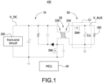
- FIG. 1 shows a circuit block diagram of an isolated converter of the present disclosure.
- the isolated converter 400 may be coupled to the front-end circuit 200 and a load 300, and the front-end circuit 200 may be a DC power supply such as an AC-to-DC converter, a power factor corrector, a DC power source, or so on.
- the isolated converter 400 includes a primary-side circuit 1B, a transformer 2B, a secondary-side circuit 3B, and a controller 4B, and the transformer 2B includes a primary-side coil 22B and a secondary-side coil 24B.
- the isolated converter 400 may be composed of the flyback converter shown in FIG. 1 . Therefore, any conversion circuit with the transformer 2B to isolate the primary side and the secondary side should be included in the scope of this embodiment.
- the primary-side circuit 1B includes a switch SW
- the secondary-side circuit 3B includes a secondary-side rectification circuit Cr.
- the secondary-side rectification circuit Cr includes a rectification switch SWr and an output capacitor Co, and the rectification switch SWr may be optionally replaced with a passive diode.
- the controller 4B controls the switch SW and the secondary-side rectification circuit Cr to store and release energy in the transformer 2B, so as to convert a DC power source V_DC received by the isolated converter 400 through the stored/released energy of the transformer 2B into an auxiliary power source V_AUX.
- the primary-side coil 22B and the secondary-side coil 24B of the transformer 2B can form a planar transformer to facilitate placement on a circuit board, and this will be further explained later and will not be described in detail here.
- the circuit structure of the primary-side circuit 1B and the secondary-side circuit 3B is only a schematic example. Any primary-side circuit 1B and the secondary-side circuit 3B that can form a structure of the isolated converter 400 are all should be included in the scope of this embodiment.
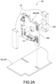
- FIG. 2A shows an exploded view of the three-dimensional circuit structure of a circuit board of the present disclosure
- FIG. 2B shows an assembly view of the three-dimensional circuit structure of the circuit board of the present disclosure, and also refer to FIG. 1 .
- the transformer 2B is configured on a circuit board CB2, and the primary-side circuit 1B, the secondary-side circuit 3B, and the controller 4B may be configured on a main circuit board CB_M2.
- Both the primary-side coil 22B and the secondary-side coil 24B of the transformer 2B have a planar trace structure, and formed on the circuit board CB2, so that the iron core C2 is directly placed on the primary-side coil 22B and the secondary-side coil 24B of the circuit board CB2 to form the transformer 2B.
- the iron core C2 includes a core pillar C22, and the core pillar C22 is directly sleeved on the circuit board CB2 through the iron core C2 and penetrates a through hole H4 of the circuit board CB2. Since the transformer 2B does not have a traditional winding frame for winding coils, and all traces are formed on the circuit board CB2, the transformer 2B has a planar structure and forms a planar transformer.
- the circuit board CB2 can be plugged into the main circuit board CB_M2 by plugging to form the circuit structure of FIG. 1 , so as to save the use space of the main circuit board CB_M2, but it does not exclude the possibility that the circuit board CB2 may be formed or configured in one of the blocks of the main circuit board CB_M2.
- the isolated converter 400 mainly forms the primary-side coil 22B and the secondary-side coil 24B of the transformer 2B on the circuit board CB2, so that the planar transformer can be planarized to significantly increase the space utilization of the isolated converter 400 to achieve high power density requirements.
- the isolated converter 400 also has a small size due to the use of a planar transformer, which can significantly increase the operating frequency of the isolated converter 400. Therefore, the rectification switch SWr of the switch SW and the secondary-side rectification circuit Cr can use third-generation semiconductor components such as wide bandgap (WBG) as the main power switch, so that the isolated converter 400 has the advantages of higher efficiency, significantly reduced power switch size, lighter weight, and increased heat dissipation performance.
- WBG wide bandgap
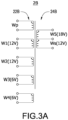
- FIG. 3A shows a circuit diagram of a transformer coil of the present disclosure
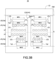
- FIG. 3B shows a schematic diagram of the transformer trace configuration of the present disclosure, and also refer to FIG. 1 to FIG. 2B
- the transformer 2B includes a primary side and a secondary side.
- the primary side includes a primary-side coil 22B and the secondary side includes a secondary-side coil 24B.
- the transformer 2B may also optionally include auxiliary coils W1, W2, W3, W4, W5, and the auxiliary coil W5 may form a center-tapped coil structure with the secondary-side coil 24B.
- the auxiliary coils W1, W2, W3, W4, W5 may couple the energy provided by the primary-side coil 22B through coupling manner, and the voltage acquired by coupling can be adjusted by adjusting the number of turns thereof. Furthermore, the auxiliary coils W1, W2, W3, W4, W5 may be used for detection of the auxiliary power source of supplying power to the load 300 according to different output voltage requirements. In one embodiment, the number of auxiliary coils W1, W2, W3, W4, W5 and their structural characteristics (independent or center-tapped, etc.) are only schematic examples and are not limited to FIG. 3A .
- FIG. 3B shows a schematic cross-sectional view of the circuit board CB2 to focus on the main features of the present disclosure, only the block of the transformer 2B is shown in the cross-sectional position.
- the circuit board CB2 is a multi-layer board (a 6-layer board is used as an example here, but is not limited to this).
- the circuit board CB2 includes a plurality of primary-side layers LP and a plurality of secondary-side layers LS, and the two sides away from the center line X are the top layer and the bottom layer of the circuit board CB2 respectively.
- a plurality of primary-side traces Tp2 are respectively formed on the primary-side layer LP of the circuit board CB2, and each primary-side layer LP includes at least one primary-side trace Tp2 that surrounds several turns (as shown in FIG. 3B with four primary-side layers LP, but not limited to this).
- the primary-side traces Tp2 may be connected in series through the interconnection of each primary-side layer LP (for example, using via holes, not shown) to serve as the primary-side coil 22B coupled to the primary-side circuit 1B.
- a plurality of secondary-side traces Ts2 are respectively formed on the secondary-side layer LS of the circuit board CB2, and each layer of the secondary-side layer LS includes at least one secondary-side trace Ts2 that surrounds several turns (as shown in FIG. 3B with two secondary-side layers Ls, but not limited to this).
- the secondary-side traces Ts2 may be connected in series through the interconnection of each secondary-side layer LS (for example, using via holes, not shown) to serve as the second second-side coil 24B coupled to the secondary-side circuit 3B.
- the material of the traces formed by each layer board may be copper foil, but it does not exclude the use of other metal foils that are easy to conduct electricity (such as but not limited to gold, silver, etc.).
- the iron core C2 surrounds the circuit board CB2, and the iron core C2 includes a core pillar C22.
- the core pillar C22 penetrates the through hole H4 of the circuit board CB2, so that the primary-side trace Tp2 and the secondary-side trace Ts2 surround the through hole H4.
- a closed magnetic circuit can be formed to form the transformer 2B. Furthermore, as shown in FIG.
- the transformer 2B is formed as follows: the primary-side trace Tp2 is close to the center of the circuit board (i.e., the center line X), and the secondary-side trace Ts2 is away from the center relative to the primary-side trace Tp2 to form a sandwich trace.
- the primary-side trace Tp2 is formed at a relatively central position in the circuit board CB2, and the secondary-side trace Ts2 is formed at a position close to the top or bottom layer of the circuit board CB2, so that the leakage inductance of the transformer 2B can be reduced and the efficiency of the isolated converter 400 can be increased.
- the trace design of the transformer 2B is not limited to the sandwich trace.
- the sandwich trace design is not adopted (for example, but not limited to, the primary-side layer LP is configured close to the top layer, and the secondary-side layer LS is configured close to the bottom layer), the coupling capacitance between the primary-side layer LP and the secondary-side layer LS can be reduced, thereby reducing noise during operation of the transformer 2B.
- the secondary-side layer LS and the primary-side layer LP respectively include a secondary-side adjacent layer LSa and a primary-side adjacent layer LPa adjacent to each other.
- a plurality of auxiliary traces Cf1, Cf2, Cf3, Cf4 are respectively formed on the primary-side adjacent layer LPa of the circuit board CB2, and the primary-side adjacent layer LPa may include at least one auxiliary trace Cf1, Cf2, Cf3, Cf4.
- the auxiliary traces Cf1, Cf2, Cf3, Cf4 can be configured in the single-layer primary-side adjacent layer LPa to form the auxiliary coils W1, W2, W3, W4, and may also be connected through each primary-side adjacent layer LPa (for example, using via holes (not shown), so that the auxiliary wirings Cf1, Cf2, Cf3, Cf4 of the same path are connected in series to serve as the auxiliary coils W1, W2, W3, W4.
- the auxiliary trace Cf5 may be formed on the secondary-side adjacent layer LSa of the circuit board CB2, and the secondary-side adjacent layer LSa may include at least one auxiliary trace Cf5.
- the auxiliary trace Cf5 may be arranged on the single-layer secondary-side adjacent layer LSa to form the auxiliary coil W5, or the auxiliary trace Cf5 on the same path may be connected in series through the interconnection of each secondary-side adjacent layer LSa (for example, using via holes, not shown) to serve as the auxiliary coil W5.
- the secondary-side layer LS is the secondary-side adjacent layer LSa
- the primary-side layer LP is the primary-side adjacent layer LPa.
- the secondary-side adjacent layer LSa includes a secondary-side trace Ts2 that surrounds the through hole H4 for several turns and an auxiliary trace Cf5.
- the primary-side adjacent layer LPa includes a primary-side trace Tp2 that surrounds the through hole H4 for several turns and at least one auxiliary trace Cf1, Cf2, Cf3, Cf4. Therefore, when the circuit board CB2 is a double-layer board, its structure and achievable functions can be inferred from the descriptions in FIG. 1 to FIG. 3B of the present disclosure and the corresponding paragraphs, and will not be described again here.
- the auxiliary traces Cf1, Cf2, Cf3, Cf4, Cf5 may selectively adjust the number of turns surrounding the through hole H4 according to the voltage required by the back-end circuit. Therefore, the auxiliary traces Cf1, Cf2, Cf3, Cf4 and the primary-side trace Tp2 may have a concentric structure (the center is the through hole H4), and the auxiliary trace Cf5 and the secondary-side trace Ts2 may have a concentric structure (the center is the through hole H4).
- the via holes described above can usually be filled with conductive materials (such as but not limited to solder paste and other conductive materials), so that the traces of the transformer 2B can be electrically connected through the via holes.
- the secondary-side trace Ts2 in the secondary-side adjacent layer LSa has a first width Wh1, Wh3, and the primary-side trace Tp2 in the primary-side adjacent layer LPa has a second width Wh2, Wh4.
- the distance from the secondary-side trace Ts2 farthest from the through hole H4 to the secondary-side trace Ts2 closest to the through hole H4 is the first width Wh1, Wh3.
- the distance from the primary-side trace Tp2 farthest from the through hole H4 to the primary-side trace Tp2 closest to the through hole H4 is the second width Wh2, Wh4.
- the "width" may be the maximum distance formed by the traces of this layer in any cross-section of the circuit board CB2 perpendicular to the center line (that is, the distance from the trace farthest from the through hole H4 to the trace closest to the through hole H4).
- the first width Wh1, Wh3 are larger than the second width Wh2, Wh4, which can make the coupling between the primary-side winding Wp and the secondary-side winding Ws better and make the voltage induced by the secondary-side winding Ws be more stable.
- the first width Wh1 formed by the secondary-side trace Ts2 of the secondary-side adjacent layer LSa can preferably cover the second width Wh2 formed by the primary-side trace Tp2 of the primary-side adjacent layer LPa. Therefore, the area formed by the secondary-side trace Ts2 of the secondary adjacent layer LSa may be larger than the area formed by the primary-side trace Tp2 of the primary-side adjacent layer LPa.
- the second width Wh2, Wh4 is formed by the auxiliary traces Cf1, Cf2, Cf3, Cf4 and the primary-side trace Tp2. That is, the first width Wh1 formed by the secondary-side trace Ts2 of the secondary-side adjacent layer LSa is preferably greater than or equal to the second width Wh2 formed by the primary-side trace Tp2 and the auxiliary traces Cf1, Cf2, Cf3, Cf4 of the primary-side adjacent layer LPa.
- the second width Wh2, Wh4 the coupling properties of the primary-side winding Wp, the secondary-side winding Ws, and the auxiliary coils W1, W2, W3, W4, W5 can be better, and the voltage induced by each coil can be more stable.
- the corresponding relationship between the first width Wh3 and the second width Wh4 is the same as the first width Wh1 and the second width Wh2, and will not be described again here.
- the auxiliary traces Cf1, Cf2, Cf3, Cf4, Cf5 may preferably be configured on the secondary-side adjacent layer LSa and the primary-side adjacent layer LPa to provide a better coupling effect, but are not limited thereto.
- the auxiliary traces Cf1, Cf2, Cf3, Cf4, Cf5 can be configured in any one of the secondary-side layer LS and the primary-side layer LP, as long as a suitable voltage can be acquired through coupling.
- the iron core C2 may also include an air gap gap to increase the magnetic resistance through the air gap configuration to avoid magnetic saturation of the transformer 2B during operation.
- the air gap gap can usually be formed on the core pillar C22, but the shaped and position of the air gap gap can be determined according to the actual requirements, and they are not limited to FIG. 3B .
- the air gap gap has a first distance Y1, and the primary-side trace Tp2, the secondary-side trace Ts2 and the through hole H4 have a plurality of second distances Y2, and the second distances Y2 are respectively greater than or equal to three times the first distance Y1.
- maintaining a specific distance between the trace and the air gap gap can reduce the cutting loss of the transformer 2B and increase the efficiency. Therefore, it is a better implementation to set the distance between the secondary-side trace Ts2 and the through hole H4 to three times the air gap gap.
- the transformer 2B forms traces on the circuit board CB2, the distance between the primary-side trace Tp2, the secondary-side trace Ts2 and the through hole H4 on each layer of the circuit board CB2 can be adjusted through simple circuit design software. Therefore, compared with the traditional transformer that can only grind the air gap on the iron core C2 and cannot adjust the coil distance, the transformer 2B of the present disclosure uses a trace structure formed on the circuit board CB2, which can achieve the effect of fine-tuning the second distance Y2.
- the auxiliary traces Cf1, Cf2, Cf3, Cf4, Cf5 may preferably have a third distance from the through hole H4, and it is a preferred implementation that the third distance is greater than or equal to three times the first distance Y1.
- FIG. 4 shows a schematic diagram of the trace configuration of the primary-side adjacent layer of the present disclosure, and also refer to FIG. 1 to FIG. 3B .
- the trace configuration of the primary-side adjacent layer LPa close to the top layer of the circuit board CB2 is illustrated, and the configuration includes the primary-side trace Tp2 and the auxiliary trace Cf1.
- the auxiliary trace Cf1 can be configured in fractional turns (that is, the number of turns of the trace of this layer around the through hole H4 is not an integer number of turns), so that the transformer 2B can fine-tune the voltage acquired to achieve the requirements of better application.
- the transformer 2B can fine-tune the voltage induced by the auxiliary trace Cf1 by configuring an additional half turn (that is, auxiliary trace Cf1 is configured with an additional half turn), 1/4 turn, or even 1/10 turn (take FIG. 4 as an example, the auxiliary trace Cf1 is 2.5 turns), so that the voltage can be more accurate (such as but not limited to 12V, etc.).
- an additional half turn that is, auxiliary trace Cf1 is configured with an additional half turn
- 1/4 turn or even 1/10 turn
- the auxiliary trace Cf1 is 2.5 turns
- the similar primary-side trace Tp2, the secondary-side trace Ts2, and the auxiliary traces Cf2, Cf3, Cf4, Cf5 can also fine-tune the induced voltage through fractional turns, and no further details will be given here.
Landscapes
- Engineering & Computer Science (AREA)
- Power Engineering (AREA)
- Chemical & Material Sciences (AREA)
- Composite Materials (AREA)
- Microelectronics & Electronic Packaging (AREA)
- Coils Or Transformers For Communication (AREA)
- Dc-Dc Converters (AREA)
- Coils Of Transformers For General Uses (AREA)
- Inverter Devices (AREA)
- Parts Printed On Printed Circuit Boards (AREA)
Abstract
Description
- The present disclosure relates to a planar transformer, and more particularly to a planar transformer applied to an isolated converter.
- The statements in this section merely provide background information related to the present disclosure and do not necessarily constitute prior art.
- With the rapid development of the information industry, power supplies have played an indispensable role. The input voltage of information and household appliances is divided into AC voltage and DC voltage, and power supplies can generally be divided into two levels. In general, the front stage is usually an AC-to-DC converter, a power factor corrector or a DC-to-DC converter, and the rear stage is usually a resonant converter. The power supply usually also includes an auxiliary circuit, and the auxiliary circuit generally converts the power provided by the front-end circuit to provide standby power, auxiliary power, and other power supplies inside the power supply that are not mainly for back-end loads.
- In particular, the auxiliary circuit can usually be an isolation converter such as a flyback converter with an isolation transformer to connect the primary side and the secondary side. However, current isolation converters usually use traditional transformers as isolated transformers, which require coils to be wound on a winding frame and an iron core to surround the winding frame to form the structure of the transformer. Since the operating frequency of traditional transformers is too low (such as but not limited to tens of kHz), it requires a larger volume. As a result, the power density of the auxiliary circuit is low, and the excessive size often makes the design difficult, which is not conducive to increase the power density and miniaturize the circuit design.
- Therefore, how to design a planar transformer to replace the traditional transformer in the isolated converter to greatly reduce the size of the isolated converter has become a critical topic in this field.
- In order to solve the above-mentioned problems, the present disclosure provides a planar transformer. The planar transformer is applied to an isolated converter, and the isolated converter includes a primary-side circuit and a secondary-side circuit. The planar transformer includes a circuit board and an iron core. The circuit board is arranged in the isolated converter, and the circuit board includes a primary-side trace and a secondary-side trace. The primary-side trace is formed on a primary-side layer of the circuit board, and the primary-side trace serves as a primary-side coil coupled to the primary-side circuit. The secondary-side trace is formed on a secondary-side layer of the circuit board, and the secondary-side trace serves as a secondary-side coil coupled to the secondary-side circuit. The iron core includes a core pillar, and the core pillar penetrates a through hole of the circuit board, and the primary-side trace and the secondary-side trace surround the through hole. The secondary-side trace has a first width and the primary-side trace has a second width, and the first width is greater than the second width.
- In order to solve the above-mentioned problems, the present disclosure provides a planar transformer. The planar transformer is applied to an isolated converter, and the isolated converter includes a primary-side circuit and a secondary-side circuit. The planar transformer includes a circuit board and an iron core. The circuit board is arranged in the isolated converter, and the circuit board includes a primary-side trace and a secondary-side trace. The primary-side trace is formed on a primary-side layer of the circuit board, and the primary-side trace serves as a primary-side coil coupled to the primary-side circuit. The secondary-side trace is formed on a secondary-side layer of the circuit board, and the secondary-side trace serves as a secondary-side coil coupled to the secondary-side circuit. The iron core includes a core pillar, and the core pillar penetrates a through hole of the circuit board, and the primary-side trace and the secondary-side trace surround the through hole. The iron core includes an air gap having a first distance; the primary-side trace, the secondary-side trace, and the through hole have a plurality of second distances, and the second distances are respectively greater than or equal to three times of the first distance.
- The main purpose and effect of the present disclosure is to replace the traditional isolation transformer in the isolation converter with the planar transformer so that the primary-side coil and the secondary-side coil are formed on the circuit board in the form of traces. Therefore, the planar transformer can be planarized to significantly increase the space utilization of the isolated converter achieve high power density requirements. In addition, the isolated converter also has a small size due to the use of a planar transformer, which can significantly increase the operating frequency of the isolated converter so that the isolated converter has the advantages of higher efficiency, significantly reduced power switch size, lighter weight, and increased heat dissipation performance.
- It is to be understood that both the foregoing general description and the following detailed description are exemplary, and are intended to provide further explanation of the present disclosure as claimed. Other advantages and features of the present disclosure will be apparent from the following description, drawings, and claims.
- The present disclosure can be more fully understood by reading the following detailed description of the embodiment, with reference made to the accompanying drawing as follows:
-
FIG. 1 is a circuit block diagram of an isolated converter of the present disclosure. -
FIG. 2A is an exploded view of the three-dimensional circuit structure of a circuit board of the present disclosure. -
FIG. 2B is an assembly view of the three-dimensional circuit structure of the circuit board of the present disclosure. -
FIG. 3A is a circuit diagram of a transformer coil of the present disclosure. -
FIG. 3B is a schematic diagram of the transformer trace configuration of the present disclosure. -
FIG. 4 is a schematic diagram of the trace configuration of the primary-side adjacent layer of the present disclosure. - Reference will now be made to the drawing figures to describe the present disclosure in detail. It will be understood that the drawing figures and exemplified embodiments of present disclosure are not limited to the details thereof.
- Please refer to
FIG. 1 , which shows a circuit block diagram of an isolated converter of the present disclosure. Theisolated converter 400 may be coupled to the front-end circuit 200 and aload 300, and the front-end circuit 200 may be a DC power supply such as an AC-to-DC converter, a power factor corrector, a DC power source, or so on. Theisolated converter 400 includes a primary-side circuit 1B, atransformer 2B, a secondary-side circuit 3B, and acontroller 4B, and thetransformer 2B includes a primary-side coil 22B and a secondary-side coil 24B. In one embodiment, for example, but not limited to, theisolated converter 400 may be composed of the flyback converter shown inFIG. 1 . Therefore, any conversion circuit with thetransformer 2B to isolate the primary side and the secondary side should be included in the scope of this embodiment. - The primary-
side circuit 1B includes a switch SW, and the secondary-side circuit 3B includes a secondary-side rectification circuit Cr. The secondary-side rectification circuit Cr includes a rectification switch SWr and an output capacitor Co, and the rectification switch SWr may be optionally replaced with a passive diode. In general, thecontroller 4B controls the switch SW and the secondary-side rectification circuit Cr to store and release energy in thetransformer 2B, so as to convert a DC power source V_DC received by the isolatedconverter 400 through the stored/released energy of thetransformer 2B into an auxiliary power source V_AUX. The primary-side coil 22B and the secondary-side coil 24B of thetransformer 2B can form a planar transformer to facilitate placement on a circuit board, and this will be further explained later and will not be described in detail here. In one embodiment, the circuit structure of the primary-side circuit 1B and the secondary-side circuit 3B is only a schematic example. Any primary-side circuit 1B and the secondary-side circuit 3B that can form a structure of the isolatedconverter 400 are all should be included in the scope of this embodiment. - Please refer to
FIG. 2A , which shows an exploded view of the three-dimensional circuit structure of a circuit board of the present disclosure; please refer toFIG. 2B , which shows an assembly view of the three-dimensional circuit structure of the circuit board of the present disclosure, and also refer toFIG. 1 . Thetransformer 2B is configured on a circuit board CB2, and the primary-side circuit 1B, the secondary-side circuit 3B, and thecontroller 4B may be configured on a main circuit board CB_M2. Both the primary-side coil 22B and the secondary-side coil 24B of thetransformer 2B have a planar trace structure, and formed on the circuit board CB2, so that the iron core C2 is directly placed on the primary-side coil 22B and the secondary-side coil 24B of the circuit board CB2 to form thetransformer 2B. In particular, the iron core C2 includes a core pillar C22, and the core pillar C22 is directly sleeved on the circuit board CB2 through the iron core C2 and penetrates a through hole H4 of the circuit board CB2. Since thetransformer 2B does not have a traditional winding frame for winding coils, and all traces are formed on the circuit board CB2, thetransformer 2B has a planar structure and forms a planar transformer. Since the planar transformer is relatively flat, the height of the circuit board CB2 is small. Therefore, the circuit board CB2 can be plugged into the main circuit board CB_M2 by plugging to form the circuit structure ofFIG. 1 , so as to save the use space of the main circuit board CB_M2, but it does not exclude the possibility that the circuit board CB2 may be formed or configured in one of the blocks of the main circuit board CB_M2. - Therefore, the
isolated converter 400 mainly forms the primary-side coil 22B and the secondary-side coil 24B of thetransformer 2B on the circuit board CB2, so that the planar transformer can be planarized to significantly increase the space utilization of theisolated converter 400 to achieve high power density requirements. In addition, theisolated converter 400 also has a small size due to the use of a planar transformer, which can significantly increase the operating frequency of theisolated converter 400. Therefore, the rectification switch SWr of the switch SW and the secondary-side rectification circuit Cr can use third-generation semiconductor components such as wide bandgap (WBG) as the main power switch, so that theisolated converter 400 has the advantages of higher efficiency, significantly reduced power switch size, lighter weight, and increased heat dissipation performance. - Please refer to
FIG. 3A , which shows a circuit diagram of a transformer coil of the present disclosure; please refer toFIG. 3B , which shows a schematic diagram of the transformer trace configuration of the present disclosure, and also refer toFIG. 1 to FIG. 2B . InFIG. 3A , thetransformer 2B includes a primary side and a secondary side. The primary side includes a primary-side coil 22B and the secondary side includes a secondary-side coil 24B. Thetransformer 2B may also optionally include auxiliary coils W1, W2, W3, W4, W5, and the auxiliary coil W5 may form a center-tapped coil structure with the secondary-side coil 24B. In particular, the auxiliary coils W1, W2, W3, W4, W5 may couple the energy provided by the primary-side coil 22B through coupling manner, and the voltage acquired by coupling can be adjusted by adjusting the number of turns thereof. Furthermore, the auxiliary coils W1, W2, W3, W4, W5 may be used for detection of the auxiliary power source of supplying power to theload 300 according to different output voltage requirements. In one embodiment, the number of auxiliary coils W1, W2, W3, W4, W5 and their structural characteristics (independent or center-tapped, etc.) are only schematic examples and are not limited toFIG. 3A . -
FIG. 3B shows a schematic cross-sectional view of the circuit board CB2 to focus on the main features of the present disclosure, only the block of thetransformer 2B is shown in the cross-sectional position. InFIG. 3B , the circuit board CB2 is a multi-layer board (a 6-layer board is used as an example here, but is not limited to this). The circuit board CB2 includes a plurality of primary-side layers LP and a plurality of secondary-side layers LS, and the two sides away from the center line X are the top layer and the bottom layer of the circuit board CB2 respectively. A plurality of primary-side traces Tp2 are respectively formed on the primary-side layer LP of the circuit board CB2, and each primary-side layer LP includes at least one primary-side trace Tp2 that surrounds several turns (as shown inFIG. 3B with four primary-side layers LP, but not limited to this). The primary-side traces Tp2 may be connected in series through the interconnection of each primary-side layer LP (for example, using via holes, not shown) to serve as the primary-side coil 22B coupled to the primary-side circuit 1B. - A plurality of secondary-side traces Ts2 are respectively formed on the secondary-side layer LS of the circuit board CB2, and each layer of the secondary-side layer LS includes at least one secondary-side trace Ts2 that surrounds several turns (as shown in
FIG. 3B with two secondary-side layers Ls, but not limited to this). The secondary-side traces Ts2 may be connected in series through the interconnection of each secondary-side layer LS (for example, using via holes, not shown) to serve as the second second-side coil 24B coupled to the secondary-side circuit 3B. In one embodiment, the material of the traces formed by each layer board may be copper foil, but it does not exclude the use of other metal foils that are easy to conduct electricity (such as but not limited to gold, silver, etc.). - The iron core C2 surrounds the circuit board CB2, and the iron core C2 includes a core pillar C22. The core pillar C22 penetrates the through hole H4 of the circuit board CB2, so that the primary-side trace Tp2 and the secondary-side trace Ts2 surround the through hole H4. After the iron core C2 is sleeved on the primary-side trace Tp2 and the secondary-side trace Ts2, a closed magnetic circuit can be formed to form the
transformer 2B. Furthermore, as shown inFIG. 3B , thetransformer 2B is formed as follows: the primary-side trace Tp2 is close to the center of the circuit board (i.e., the center line X), and the secondary-side trace Ts2 is away from the center relative to the primary-side trace Tp2 to form a sandwich trace. - That is, the primary-side trace Tp2 is formed at a relatively central position in the circuit board CB2, and the secondary-side trace Ts2 is formed at a position close to the top or bottom layer of the circuit board CB2, so that the leakage inductance of the
transformer 2B can be reduced and the efficiency of theisolated converter 400 can be increased. In particular, the trace design of thetransformer 2B is not limited to the sandwich trace. Specifically, if the sandwich trace design is not adopted (for example, but not limited to, the primary-side layer LP is configured close to the top layer, and the secondary-side layer LS is configured close to the bottom layer), the coupling capacitance between the primary-side layer LP and the secondary-side layer LS can be reduced, thereby reducing noise during operation of thetransformer 2B. - On the other hand, the secondary-side layer LS and the primary-side layer LP respectively include a secondary-side adjacent layer LSa and a primary-side adjacent layer LPa adjacent to each other. A plurality of auxiliary traces Cf1, Cf2, Cf3, Cf4 are respectively formed on the primary-side adjacent layer LPa of the circuit board CB2, and the primary-side adjacent layer LPa may include at least one auxiliary trace Cf1, Cf2, Cf3, Cf4. The auxiliary traces Cf1, Cf2, Cf3, Cf4 can be configured in the single-layer primary-side adjacent layer LPa to form the auxiliary coils W1, W2, W3, W4, and may also be connected through each primary-side adjacent layer LPa (for example, using via holes (not shown), so that the auxiliary wirings Cf1, Cf2, Cf3, Cf4 of the same path are connected in series to serve as the auxiliary coils W1, W2, W3, W4.
- Similarly, the auxiliary trace Cf5 may be formed on the secondary-side adjacent layer LSa of the circuit board CB2, and the secondary-side adjacent layer LSa may include at least one auxiliary trace Cf5. The auxiliary trace Cf5 may be arranged on the single-layer secondary-side adjacent layer LSa to form the auxiliary coil W5, or the auxiliary trace Cf5 on the same path may be connected in series through the interconnection of each secondary-side adjacent layer LSa (for example, using via holes, not shown) to serve as the auxiliary coil W5. In addition, when the number of layers of the secondary-side layer LS and the primary-side layer LP is one (that is, the circuit board CB2 is a double-layer board and includes the top layer and the bottom layer), the secondary-side layer LS is the secondary-side adjacent layer LSa, and the primary-side layer LP is the primary-side adjacent layer LPa. The secondary-side adjacent layer LSa includes a secondary-side trace Ts2 that surrounds the through hole H4 for several turns and an auxiliary trace Cf5. The primary-side adjacent layer LPa includes a primary-side trace Tp2 that surrounds the through hole H4 for several turns and at least one auxiliary trace Cf1, Cf2, Cf3, Cf4. Therefore, when the circuit board CB2 is a double-layer board, its structure and achievable functions can be inferred from the descriptions in
FIG. 1 to FIG. 3B of the present disclosure and the corresponding paragraphs, and will not be described again here. - In particular, the auxiliary traces Cf1, Cf2, Cf3, Cf4, Cf5 may selectively adjust the number of turns surrounding the through hole H4 according to the voltage required by the back-end circuit. Therefore, the auxiliary traces Cf1, Cf2, Cf3, Cf4 and the primary-side trace Tp2 may have a concentric structure (the center is the through hole H4), and the auxiliary trace Cf5 and the secondary-side trace Ts2 may have a concentric structure (the center is the through hole H4). In particular, the via holes described above can usually be filled with conductive materials (such as but not limited to solder paste and other conductive materials), so that the traces of the
transformer 2B can be electrically connected through the via holes. - In
FIG. 3B , the secondary-side trace Ts2 in the secondary-side adjacent layer LSa has a first width Wh1, Wh3, and the primary-side trace Tp2 in the primary-side adjacent layer LPa has a second width Wh2, Wh4. Specifically, in the secondary-side adjacent layer LSa, the distance from the secondary-side trace Ts2 farthest from the through hole H4 to the secondary-side trace Ts2 closest to the through hole H4 is the first width Wh1, Wh3. In the primary-side adjacent layer LPa, the distance from the primary-side trace Tp2 farthest from the through hole H4 to the primary-side trace Tp2 closest to the through hole H4 is the second width Wh2, Wh4. In particular, the "width" may be the maximum distance formed by the traces of this layer in any cross-section of the circuit board CB2 perpendicular to the center line (that is, the distance from the trace farthest from the through hole H4 to the trace closest to the through hole H4). In one embodiment, the first width Wh1, Wh3 are larger than the second width Wh2, Wh4, which can make the coupling between the primary-side winding Wp and the secondary-side winding Ws better and make the voltage induced by the secondary-side winding Ws be more stable. That is, in the secondary-side adjacent layer LSa close to the top layer, the first width Wh1 formed by the secondary-side trace Ts2 of the secondary-side adjacent layer LSa can preferably cover the second width Wh2 formed by the primary-side trace Tp2 of the primary-side adjacent layer LPa. Therefore, the area formed by the secondary-side trace Ts2 of the secondary adjacent layer LSa may be larger than the area formed by the primary-side trace Tp2 of the primary-side adjacent layer LPa. - In addition, when the primary-side adjacent layer LPa includes the primary-side trace Tp2 and the auxiliary traces Cf1, Cf2, Cf3, Cf4, the second width Wh2, Wh4 is formed by the auxiliary traces Cf1, Cf2, Cf3, Cf4 and the primary-side trace Tp2. That is, the first width Wh1 formed by the secondary-side trace Ts2 of the secondary-side adjacent layer LSa is preferably greater than or equal to the second width Wh2 formed by the primary-side trace Tp2 and the auxiliary traces Cf1, Cf2, Cf3, Cf4 of the primary-side adjacent layer LPa. In particular, in the primary-side adjacent layer LPa, from the trace farthest from the through hole H4 (which may be the primary-side trace Tp2 or one of the auxiliary traces Cf1, Cf2, Cf3, Cf4) to the trace closest to the through hole H4 (which may be the primary-side trace Tp2 or another of the auxiliary traces Cf1, Cf2, Cf3, Cf4) is the second width Wh2, Wh4. Therefore, the coupling properties of the primary-side winding Wp, the secondary-side winding Ws, and the auxiliary coils W1, W2, W3, W4, W5 can be better, and the voltage induced by each coil can be more stable.
- In one embodiment, the corresponding relationship between the first width Wh3 and the second width Wh4 is the same as the first width Wh1 and the second width Wh2, and will not be described again here. In addition, the auxiliary traces Cf1, Cf2, Cf3, Cf4, Cf5 may preferably be configured on the secondary-side adjacent layer LSa and the primary-side adjacent layer LPa to provide a better coupling effect, but are not limited thereto. In other words, the auxiliary traces Cf1, Cf2, Cf3, Cf4, Cf5 can be configured in any one of the secondary-side layer LS and the primary-side layer LP, as long as a suitable voltage can be acquired through coupling.
- In
FIG. 3B , the iron core C2 may also include an air gap gap to increase the magnetic resistance through the air gap configuration to avoid magnetic saturation of thetransformer 2B during operation. The air gap gap can usually be formed on the core pillar C22, but the shaped and position of the air gap gap can be determined according to the actual requirements, and they are not limited toFIG. 3B . In particular, the air gap gap has a first distance Y1, and the primary-side trace Tp2, the secondary-side trace Ts2 and the through hole H4 have a plurality of second distances Y2, and the second distances Y2 are respectively greater than or equal to three times the first distance Y1. Specifically, maintaining a specific distance between the trace and the air gap gap can reduce the cutting loss of thetransformer 2B and increase the efficiency. Therefore, it is a better implementation to set the distance between the secondary-side trace Ts2 and the through hole H4 to three times the air gap gap. - On the other hand, since the
transformer 2B forms traces on the circuit board CB2, the distance between the primary-side trace Tp2, the secondary-side trace Ts2 and the through hole H4 on each layer of the circuit board CB2 can be adjusted through simple circuit design software. Therefore, compared with the traditional transformer that can only grind the air gap on the iron core C2 and cannot adjust the coil distance, thetransformer 2B of the present disclosure uses a trace structure formed on the circuit board CB2, which can achieve the effect of fine-tuning the second distance Y2. In addition, the auxiliary traces Cf1, Cf2, Cf3, Cf4, Cf5 may preferably have a third distance from the through hole H4, and it is a preferred implementation that the third distance is greater than or equal to three times the first distance Y1. - Please refer to
FIG. 4 , which shows a schematic diagram of the trace configuration of the primary-side adjacent layer of the present disclosure, and also refer toFIG. 1 to FIG. 3B . InFIG. 4 , the trace configuration of the primary-side adjacent layer LPa close to the top layer of the circuit board CB2 is illustrated, and the configuration includes the primary-side trace Tp2 and the auxiliary trace Cf1. InFIG. 4 , the auxiliary trace Cf1 can be configured in fractional turns (that is, the number of turns of the trace of this layer around the through hole H4 is not an integer number of turns), so that thetransformer 2B can fine-tune the voltage acquired to achieve the requirements of better application. Specifically, in order to make the voltage value of the output voltage more stable and finely adjusted, thetransformer 2B can fine-tune the voltage induced by the auxiliary trace Cf1 by configuring an additional half turn (that is, auxiliary trace Cf1 is configured with an additional half turn), 1/4 turn, or even 1/10 turn (takeFIG. 4 as an example, the auxiliary trace Cf1 is 2.5 turns), so that the voltage can be more accurate (such as but not limited to 12V, etc.). In particular, although only the number of turns of the auxiliary trace Cf1 surrounding the through hole H4 is shown inFIG. 4 , which is not an integer number of turns, the similar primary-side trace Tp2, the secondary-side trace Ts2, and the auxiliary traces Cf2, Cf3, Cf4, Cf5 can also fine-tune the induced voltage through fractional turns, and no further details will be given here.
Claims (14)
- A planar transformer (2B) applied to an isolated converter (400), the isolated converter (400) comprising a primary-side circuit (1B) and a secondary-side circuit (3B), characterized in that the planar transformer (2B) comprising:
a circuit board (CB2) arranged in the isolated converter (400), the circuit board (CB2) comprising:a primary-side trace (Tp2) formed on a primary-side layer (LP) of the circuit board (CB2), and the primary-side trace (Tp2) configured to serve as a primary-side coil (22B) coupled to the primary-side circuit (1B), anda secondary-side trace (Ts2) formed on a secondary-side layer (LS) of the circuit board (CB2), and the secondary-side trace (Ts2) configured to serve as a secondary-side coil (24B) coupled to the secondary-side circuit (3B), andan iron core (C2) comprising a core pillar (C22), the core pillar (C22) penetrating a through hole (H4) of the circuit board (CB2), and the primary-side trace (Tp2) and the secondary-side trace (Ts2) surrounding the through hole (H4),wherein the secondary-side trace (Ts2) has a first width (Wh1, Wh3) and the primary-side trace (Tp2) has a second width (Wh2, Wh4), and the first width (Wh1, Wh3) is greater than the second width (Wh2, Wh4). - The planar transformer (2B) as claimed in claim 1, wherein the number of the primary-side layers (LP) is plural and the number of the secondary-side layers (LS) is plural; each primary-side layer (LP) comprises the primary-side trace (Tp2), and each secondary-side layer (LS) comprises the secondary-side trace (Ts2); the primary-side traces (Tp2) are close to a center of the circuit board (CB2) and the secondary-side traces (Ts2) are away from the center to form a sandwich trace.
- The planar transformer (2B) as claimed in claim 1, wherein the circuit board (CB2) further comprises:at least one auxiliary trace (Cfl, Cf2, Cf3, Cf4, Cf5) formed on the primary-side layer (LP) to serve as at least one auxiliary coil (W1, W2, W3, W4, W5),wherein the at least one auxiliary trace (Cfl, Cf2, Cf3, Cf4, Cf5) surrounds the through hole (H4) to form a concentric structure with the primary-side trace (Tp2).
- The planar transformer (2B) as claimed in claim 3, wherein the second width (Wh2, Wh4) is formed by the at least one auxiliary trace (Cfl, Cf2, Cf3, Cf4, Cf5) and the primary-side trace (Tp2), and the first width (Wh1, Wh3) is greater than or equal to the second width (Wh2, Wh4).
- The planar transformer (2B) as claimed in claim 3, wherein the number of turns of surrounding the hole of at least one of the primary-side trace (Tp2), the secondary-side trace (Ts2), and the at least one auxiliary trace (Cfl, Cf2, Cf3, Cf4, Cf5) is not an integer.
- The planar transformer (2B) as claimed in claim 1, wherein the primary-side circuit (1B) and the secondary-side circuit (3B) are arranged on a main circuit board (CB_M2), and the circuit board (CB2) is plugged into the main circuit board (CB_M2).
- A planar transformer (2B) applied to an isolated converter (400), the isolated converter (400) comprising a primary-side circuit (1B) and a secondary-side circuit (3B), characterized in that the planar transformer (2B) comprising:
a circuit board (CB2) arranged in the isolated converter (400), the circuit board (CB2) comprising:a primary-side trace (Tp2) formed on a primary-side layer (LP) of the circuit board (CB2), and the primary-side trace (Tp2) configured to serve as a primary-side coil (22B) coupled to the primary-side circuit (1B), anda secondary-side trace (Ts2) formed on a secondary-side layer (LS) of the circuit board (CB2), and the secondary-side trace (Ts2) configured to serve as a secondary-side coil (24B) coupled to the secondary-side circuit (3B), andan iron core (C2) comprising a core pillar (C22), the core pillar (C22) penetrating a through hole (H4) of the circuit board (CB2), and the primary-side trace (Tp2) and the secondary-side trace (Ts2) surrounding the through hole (H4),wherein the iron core (C2) comprises an air gap (gap) having a first distance (Y1); the primary-side trace (Tp2), the secondary-side trace (Ts2), and the through hole (H4) have a plurality of second distances (Y2), and the second distances (Y2) are respectively greater than or equal to three times of the first distance (Y1). - The planar transformer (2B) as claimed in claim 7, wherein the secondary-side trace (Ts2) has a first width (Wh1, Wh3) and the primary-side trace (Tp2) has a second width (Wh2, Wh4), and the first width (Wh1, Wh3) is greater than the second width (Wh2, Wh4).
- The planar transformer (2B) as claimed in claim 7, wherein the number of the primary-side layers (LP) is plural and the number of the secondary-side layers (LS) is plural; each primary-side layer (LP) comprises the primary-side trace (Tp2), and each secondary-side layer (LS) comprises the secondary-side trace (Ts2); the primary-side traces (Tp2) are close to a center of the circuit board (CB2) and the secondary-side traces (Ts2) are away from the center to form a sandwich trace.
- The planar transformer (2B) as claimed in claim 7, wherein the circuit board (CB2) further comprises:at least one auxiliary trace (Cfl, Cf2, Cf3, Cf4, Cf5) formed on the primary-side layer (LP) to serve as at least one auxiliary coil (W1, W2, W3, W4, W5),wherein the at least one auxiliary trace (Cfl, Cf2, Cf3, Cf4, Cf5) surrounds the through hole (H4) to form a concentric structure with the primary-side trace (Tp2).
- The planar transformer (2B) as claimed in claim 10, wherein the at least one auxiliary trace (Cfl, Cf2, Cf3, Cf4, Cf5) and the through hole (H4) have at least one third distance (Y3), and the at least one third distance (Y3) is greater than or equal to three times of the first distance (Y1).
- The planar transformer (2B) as claimed in claim 10, wherein the number of turns of surrounding the hole of at least one of the primary-side trace (Tp2), the secondary-side trace (Ts2), and the at least one auxiliary trace (Cfl, Cf2, Cf3, Cf4, Cf5) is not an integer.
- The planar transformer (2B) as claimed in claim 10, wherein the second width (Wh2, Wh4) is formed by at least one auxiliary trace (Cfl, Cf2, Cf3, Cf4, Cf5) and the primary-side trace (Tp2), and the first width (Wh1, Wh3) is greater than or equal to the second width (Wh2, Wh4).
- The planar transformer (2B) as claimed in claim 7, wherein the primary-side circuit (1B) and the secondary-side circuit (3B) are arranged on a main circuit board (CB_M2), and the circuit board (CB2) is plugged into the main circuit board (CB_M2).
Applications Claiming Priority (1)
| Application Number | Priority Date | Filing Date | Title |
|---|---|---|---|
| US202263425014P | 2022-11-14 | 2022-11-14 |
Publications (2)
| Publication Number | Publication Date |
|---|---|
| EP4369363A2 true EP4369363A2 (en) | 2024-05-15 |
| EP4369363A3 EP4369363A3 (en) | 2024-07-10 |
Family
ID=88833518
Family Applications (5)
| Application Number | Title | Priority Date | Filing Date |
|---|---|---|---|
| EP23209486.2A Pending EP4369586A1 (en) | 2022-11-14 | 2023-11-13 | Power supply unit and dc conversion module |
| EP23209562.0A Pending EP4369365A1 (en) | 2022-11-14 | 2023-11-13 | Planar transformer |
| EP23209566.1A Active EP4369366B1 (en) | 2022-11-14 | 2023-11-13 | Planar magnetic component |
| EP23209485.4A Pending EP4369364A1 (en) | 2022-11-14 | 2023-11-13 | Planar magnetic component |
| EP23209405.2A Pending EP4369363A3 (en) | 2022-11-14 | 2023-11-13 | Planar transformer |
Family Applications Before (4)
| Application Number | Title | Priority Date | Filing Date |
|---|---|---|---|
| EP23209486.2A Pending EP4369586A1 (en) | 2022-11-14 | 2023-11-13 | Power supply unit and dc conversion module |
| EP23209562.0A Pending EP4369365A1 (en) | 2022-11-14 | 2023-11-13 | Planar transformer |
| EP23209566.1A Active EP4369366B1 (en) | 2022-11-14 | 2023-11-13 | Planar magnetic component |
| EP23209485.4A Pending EP4369364A1 (en) | 2022-11-14 | 2023-11-13 | Planar magnetic component |
Country Status (4)
| Country | Link |
|---|---|
| US (5) | US20240161966A1 (en) |
| EP (5) | EP4369586A1 (en) |
| CN (6) | CN118039312A (en) |
| TW (7) | TWI852831B (en) |
Families Citing this family (3)
| Publication number | Priority date | Publication date | Assignee | Title |
|---|---|---|---|---|
| US12537557B2 (en) * | 2022-08-30 | 2026-01-27 | Texas Instruments Incorporated | Differential electrical balance duplexers |
| US20250293595A1 (en) * | 2024-03-15 | 2025-09-18 | Delta Electronics, Inc. | Resonant converter |
| KR20260011460A (en) * | 2024-07-16 | 2026-01-23 | 현대모비스 주식회사 | Flat Transformer |
Family Cites Families (30)
| Publication number | Priority date | Publication date | Assignee | Title |
|---|---|---|---|---|
| JP2002299130A (en) * | 2001-04-02 | 2002-10-11 | Densei Lambda Kk | Composite element for power source |
| JP5359749B2 (en) * | 2009-09-30 | 2013-12-04 | Tdk株式会社 | Transformer and switching power supply |
| CN101917053B (en) * | 2010-08-03 | 2012-10-24 | 浪潮电子信息产业股份有限公司 | Method for carrying out centralized power supply on RACK system |
| US9467054B2 (en) * | 2013-11-07 | 2016-10-11 | Futurewei Technologies, Inc. | Current sensing apparatus for resonant tank in an LLC resonant converter |
| CN105655113B (en) * | 2014-11-12 | 2018-04-17 | 台达电子工业股份有限公司 | PCB planar transformer and converter using same |
| CN106484045B (en) * | 2015-08-25 | 2020-06-30 | 佛山市顺德区顺达电脑厂有限公司 | Server |
| TWI542135B (en) * | 2015-09-11 | 2016-07-11 | 萬國半導體(開曼)股份有限公司 | Voltage converter |
| WO2017133383A1 (en) * | 2016-02-05 | 2017-08-10 | 广东欧珀移动通信有限公司 | Adapter and charge control method |
| WO2017173603A1 (en) * | 2016-04-06 | 2017-10-12 | Telefonaktiebolaget Lm Ericsson (Publ) | Power converter |
| US20210050142A1 (en) * | 2016-05-25 | 2021-02-18 | Delta Electronics (Shanghai) Co., Ltd. | Power module and power device |
| CN106655721A (en) * | 2017-03-13 | 2017-05-10 | 杭州富特科技股份有限公司 | Power supply power module and circuit board combination thereof, and power converter |
| CN109412389B (en) * | 2017-08-15 | 2020-11-06 | 泰达电子股份有限公司 | Power supply conversion device |
| CN107818865B (en) * | 2017-09-19 | 2019-05-31 | 东南大学 | A kind of high frequency centre tap flat surface transformer in LLC half bridge resonant |
| TWI630628B (en) * | 2017-10-19 | 2018-07-21 | 光壽科技有限公司 | Capacitive resistance voltage conversion device |
| EP3629463A1 (en) * | 2018-09-27 | 2020-04-01 | Siemens Aktiengesellschaft | Resonant direct current regulator |
| CN109494749B (en) * | 2018-11-30 | 2021-03-26 | 华中科技大学 | Plug-and-play integrated modular series dynamic voltage compensator |
| CN111383830B (en) * | 2018-12-29 | 2021-05-28 | 台达电子企业管理(上海)有限公司 | Magnetic unit |
| CN109546872B (en) * | 2019-01-22 | 2023-09-15 | 东莞育嘉电子有限公司 | Infinitely expandable power supply system with parallel stacking |
| JP6988839B2 (en) * | 2019-02-01 | 2022-01-05 | オムロン株式会社 | Resonant converter control circuit and its control method and resonant converter |
| US11848140B2 (en) * | 2019-06-11 | 2023-12-19 | Virginia Tech Intellectual Properties, Inc. | Integrated parallel matrix transformer and inductor |
| CN112564485B (en) * | 2019-09-10 | 2022-03-08 | 中车株洲电力机车研究所有限公司 | LLC resonant converter and control method thereof |
| CN111463879A (en) * | 2020-04-29 | 2020-07-28 | 恩益达电源科技(苏州)有限公司 | A power control system for charging piles |
| DE102020118708A1 (en) * | 2020-07-15 | 2022-01-20 | WAGO Verwaltungsgesellschaft mit beschränkter Haftung | ELECTRICAL ARRANGEMENT WITH TRANSFORMER FOR TRANSMITTING SIGNALS FROM A PRIMARY SIDE TO A SECONDARY SIDE |
| BR112023001123A2 (en) * | 2020-07-21 | 2023-03-28 | Omnifi Inc | FLEXIBLE WIRELESS INTERCONNECTION AND PLATE DIVERSITY |
| US11594973B2 (en) * | 2020-08-04 | 2023-02-28 | Delta Electronics Inc. | Multiple-port bidirectional converter and control method thereof |
| TWM612250U (en) * | 2021-01-14 | 2021-05-21 | 台達電子工業股份有限公司 | Magnetic element |
| US20230162905A1 (en) * | 2021-02-08 | 2023-05-25 | Navitas Semiconductor Limited | Planar transformer including noise cancellation for auxiliary winding |
| US11638359B2 (en) * | 2021-05-05 | 2023-04-25 | Toyota Motor Engineering & Manufacturing North America, Inc. | Low profile power module package |
| US20230005659A1 (en) * | 2021-07-05 | 2023-01-05 | Navitas Semiconductor Limited | Systems and methods for improving winding losses in planar transformers |
| WO2024077528A1 (en) * | 2022-10-12 | 2024-04-18 | Innoscience (Shenzhen) Semiconductor Co., Ltd. | GaN-BASED SWITCHED-MODE POWER SUPPLY WITH PLANAR TRANSFORMER |
-
2023
- 2023-11-13 CN CN202311504362.XA patent/CN118039312A/en active Pending
- 2023-11-13 TW TW112143654A patent/TWI852831B/en active
- 2023-11-13 CN CN202311506112.XA patent/CN118039314A/en active Pending
- 2023-11-13 TW TW112143640A patent/TWI879226B/en active
- 2023-11-13 EP EP23209486.2A patent/EP4369586A1/en active Pending
- 2023-11-13 EP EP23209562.0A patent/EP4369365A1/en active Pending
- 2023-11-13 TW TW112143653A patent/TWI891121B/en active
- 2023-11-13 EP EP23209566.1A patent/EP4369366B1/en active Active
- 2023-11-13 US US18/507,446 patent/US20240161966A1/en active Pending
- 2023-11-13 CN CN202311504360.0A patent/CN118039311A/en active Pending
- 2023-11-13 EP EP23209485.4A patent/EP4369364A1/en active Pending
- 2023-11-13 TW TW112212259U patent/TWM656161U/en unknown
- 2023-11-13 TW TW112143629A patent/TWI890192B/en active
- 2023-11-13 EP EP23209405.2A patent/EP4369363A3/en active Pending
- 2023-11-13 CN CN202323055274.4U patent/CN221551625U/en active Active
- 2023-11-13 TW TW112143628A patent/TWI872803B/en active
- 2023-11-13 CN CN202311504365.3A patent/CN118041064A/en active Pending
- 2023-11-13 US US18/507,694 patent/US20240161967A1/en active Pending
- 2023-11-13 CN CN202311504363.4A patent/CN118039313A/en active Pending
- 2023-11-13 US US18/507,853 patent/US20240162833A1/en active Pending
- 2023-11-13 TW TW114100115A patent/TWI915160B/en active
- 2023-11-13 US US18/507,775 patent/US20240161969A1/en active Pending
- 2023-11-13 US US18/507,751 patent/US20240161968A1/en active Pending
Also Published As
| Publication number | Publication date |
|---|---|
| CN118039314A (en) | 2024-05-14 |
| EP4369366B1 (en) | 2025-04-09 |
| TW202518826A (en) | 2025-05-01 |
| TWI872803B (en) | 2025-02-11 |
| US20240162833A1 (en) | 2024-05-16 |
| TW202420345A (en) | 2024-05-16 |
| TWI890192B (en) | 2025-07-11 |
| TWI852831B (en) | 2024-08-11 |
| US20240161967A1 (en) | 2024-05-16 |
| TW202420723A (en) | 2024-05-16 |
| TW202420346A (en) | 2024-05-16 |
| US20240161968A1 (en) | 2024-05-16 |
| US20240161969A1 (en) | 2024-05-16 |
| TW202429494A (en) | 2024-07-16 |
| CN118041064A (en) | 2024-05-14 |
| CN118039312A (en) | 2024-05-14 |
| CN118039311A (en) | 2024-05-14 |
| CN118039313A (en) | 2024-05-14 |
| TWI891121B (en) | 2025-07-21 |
| EP4369366A1 (en) | 2024-05-15 |
| EP4369586A1 (en) | 2024-05-15 |
| CN221551625U (en) | 2024-08-16 |
| TWI879226B (en) | 2025-04-01 |
| EP4369363A3 (en) | 2024-07-10 |
| TW202427508A (en) | 2024-07-01 |
| US20240161966A1 (en) | 2024-05-16 |
| TWM656161U (en) | 2024-06-01 |
| EP4369364A1 (en) | 2024-05-15 |
| EP4369365A1 (en) | 2024-05-15 |
| TWI915160B (en) | 2026-02-11 |
Similar Documents
| Publication | Publication Date | Title |
|---|---|---|
| US20240161967A1 (en) | Planar transformer | |
| US7671713B2 (en) | Integrated structure of passive elements in LLC resonance converter realized by flexible circuit boards | |
| Nabih et al. | Magnetic integration of four-transformer matrix with high controllable leakage inductance using a five-leg magnetic | |
| Sun et al. | Integrated magnetics for current-doubler rectifiers | |
| EP2264882A1 (en) | Switching power supply unit | |
| US11489449B2 (en) | Adjustable leakage inductance transformer | |
| CN206421898U (en) | PCB flat-plate transformers with tap | |
| Kim et al. | High efficiency slim adapter with low profile transformer structure | |
| CN217769886U (en) | Magnetic integrated assembly, resonant converter and power supply | |
| TWI905041B (en) | Resonant converter | |
| CN219418708U (en) | PFC inductor of crisscross parallelly connected of magnetism integration | |
| CN114499193A (en) | LCLCL resonant converter based on matrix transformer and manufacturing method thereof | |
| CN221598235U (en) | Circuit board for realizing high-voltage isolation and power superposition based on planar transformer | |
| US20250273384A1 (en) | Planar transformer assembly and power adapter | |
| EP4583131A1 (en) | Transformer and llc resonant converter comprising same | |
| KR101251842B1 (en) | Transformer | |
| US12488929B2 (en) | Magnetic apparatus, and voltage converter including the same | |
| Nabih et al. | 3kW power supply design with easy manufacturability for 48 V bus power architecture | |
| KR20250093221A (en) | An integrated power supply using a planar energy transfer element | |
| Lin et al. | Comparison of Conventional and Planar Transformers in Server Power Supply Application | |
| Nabih et al. | A Method to Embed Resonant Inductor within PCB Matrix Transformer for High-Density Resonant Converters | |
| CN121483826A (en) | A magnetic integrated converter for fixed switching frequency resonant conversion | |
| Abnavi | High Frequency Class DE Converter Using a Multilayer Coreless PCB Transformer |
Legal Events
| Date | Code | Title | Description |
|---|---|---|---|
| PUAI | Public reference made under article 153(3) epc to a published international application that has entered the european phase |
Free format text: ORIGINAL CODE: 0009012 |
|
| STAA | Information on the status of an ep patent application or granted ep patent |
Free format text: STATUS: THE APPLICATION HAS BEEN PUBLISHED |
|
| AK | Designated contracting states |
Kind code of ref document: A2 Designated state(s): AL AT BE BG CH CY CZ DE DK EE ES FI FR GB GR HR HU IE IS IT LI LT LU LV MC ME MK MT NL NO PL PT RO RS SE SI SK SM TR |
|
| PUAL | Search report despatched |
Free format text: ORIGINAL CODE: 0009013 |
|
| AK | Designated contracting states |
Kind code of ref document: A3 Designated state(s): AL AT BE BG CH CY CZ DE DK EE ES FI FR GB GR HR HU IE IS IT LI LT LU LV MC ME MK MT NL NO PL PT RO RS SE SI SK SM TR |
|
| RIC1 | Information provided on ipc code assigned before grant |
Ipc: H02M 3/335 20060101ALI20240604BHEP Ipc: H02M 3/158 20060101ALI20240604BHEP Ipc: H01F 27/34 20060101ALI20240604BHEP Ipc: H01F 27/40 20060101ALI20240604BHEP Ipc: H01F 27/28 20060101AFI20240604BHEP |
|
| STAA | Information on the status of an ep patent application or granted ep patent |
Free format text: STATUS: REQUEST FOR EXAMINATION WAS MADE |
|
| 17P | Request for examination filed |
Effective date: 20240909 |
|
| RBV | Designated contracting states (corrected) |
Designated state(s): AL AT BE BG CH CY CZ DE DK EE ES FI FR GB GR HR HU IE IS IT LI LT LU LV MC ME MK MT NL NO PL PT RO RS SE SI SK SM TR |