EP4369063A1 - Method for manufacturing diffraction lattice and method for manufacturing replica diffraction lattice - Google Patents
Method for manufacturing diffraction lattice and method for manufacturing replica diffraction lattice Download PDFInfo
- Publication number
- EP4369063A1 EP4369063A1 EP22835555.8A EP22835555A EP4369063A1 EP 4369063 A1 EP4369063 A1 EP 4369063A1 EP 22835555 A EP22835555 A EP 22835555A EP 4369063 A1 EP4369063 A1 EP 4369063A1
- Authority
- EP
- European Patent Office
- Prior art keywords
- metal film
- glass substrate
- diffraction grating
- opening
- manufacturing
- Prior art date
- Legal status (The legal status is an assumption and is not a legal conclusion. Google has not performed a legal analysis and makes no representation as to the accuracy of the status listed.)
- Pending
Links
- 238000000034 method Methods 0.000 title claims description 57
- 238000004519 manufacturing process Methods 0.000 title claims description 41
- 229910052751 metal Inorganic materials 0.000 claims abstract description 139
- 239000002184 metal Substances 0.000 claims abstract description 139
- 239000011521 glass Substances 0.000 claims abstract description 102
- 239000000758 substrate Substances 0.000 claims abstract description 99
- 238000012546 transfer Methods 0.000 claims abstract description 40
- 239000007767 bonding agent Substances 0.000 claims abstract description 37
- 229920005989 resin Polymers 0.000 claims description 24
- 239000011347 resin Substances 0.000 claims description 24
- 239000000463 material Substances 0.000 claims description 17
- 238000003825 pressing Methods 0.000 claims description 6
- 238000010438 heat treatment Methods 0.000 claims description 5
- 238000007747 plating Methods 0.000 claims description 3
- 238000001579 optical reflectometry Methods 0.000 claims description 2
- XUIMIQQOPSSXEZ-UHFFFAOYSA-N Silicon Chemical compound [Si] XUIMIQQOPSSXEZ-UHFFFAOYSA-N 0.000 description 13
- 229910052710 silicon Inorganic materials 0.000 description 13
- 239000010703 silicon Substances 0.000 description 13
- 230000003287 optical effect Effects 0.000 description 6
- 230000037303 wrinkles Effects 0.000 description 6
- 230000000694 effects Effects 0.000 description 3
- 238000009713 electroplating Methods 0.000 description 3
- 230000002093 peripheral effect Effects 0.000 description 3
- 238000001020 plasma etching Methods 0.000 description 3
- 239000004065 semiconductor Substances 0.000 description 3
- RYGMFSIKBFXOCR-UHFFFAOYSA-N Copper Chemical compound [Cu] RYGMFSIKBFXOCR-UHFFFAOYSA-N 0.000 description 2
- PXHVJJICTQNCMI-UHFFFAOYSA-N Nickel Chemical compound [Ni] PXHVJJICTQNCMI-UHFFFAOYSA-N 0.000 description 2
- 229910052782 aluminium Inorganic materials 0.000 description 2
- XAGFODPZIPBFFR-UHFFFAOYSA-N aluminium Chemical compound [Al] XAGFODPZIPBFFR-UHFFFAOYSA-N 0.000 description 2
- 239000004020 conductor Substances 0.000 description 2
- 230000008602 contraction Effects 0.000 description 2
- 229910052802 copper Inorganic materials 0.000 description 2
- 239000010949 copper Substances 0.000 description 2
- 238000009826 distribution Methods 0.000 description 2
- 238000009434 installation Methods 0.000 description 2
- BASFCYQUMIYNBI-UHFFFAOYSA-N platinum Chemical compound [Pt] BASFCYQUMIYNBI-UHFFFAOYSA-N 0.000 description 2
- 238000012545 processing Methods 0.000 description 2
- 229910001220 stainless steel Inorganic materials 0.000 description 2
- 239000010935 stainless steel Substances 0.000 description 2
- 238000007740 vapor deposition Methods 0.000 description 2
- VYZAMTAEIAYCRO-UHFFFAOYSA-N Chromium Chemical compound [Cr] VYZAMTAEIAYCRO-UHFFFAOYSA-N 0.000 description 1
- RTAQQCXQSZGOHL-UHFFFAOYSA-N Titanium Chemical compound [Ti] RTAQQCXQSZGOHL-UHFFFAOYSA-N 0.000 description 1
- 229910052804 chromium Inorganic materials 0.000 description 1
- 239000011651 chromium Substances 0.000 description 1
- 238000000576 coating method Methods 0.000 description 1
- 238000001312 dry etching Methods 0.000 description 1
- 239000003822 epoxy resin Substances 0.000 description 1
- 238000005530 etching Methods 0.000 description 1
- 238000007687 exposure technique Methods 0.000 description 1
- PCHJSUWPFVWCPO-UHFFFAOYSA-N gold Chemical compound [Au] PCHJSUWPFVWCPO-UHFFFAOYSA-N 0.000 description 1
- 229910052737 gold Inorganic materials 0.000 description 1
- 239000010931 gold Substances 0.000 description 1
- 239000000203 mixture Substances 0.000 description 1
- 238000012986 modification Methods 0.000 description 1
- 230000004048 modification Effects 0.000 description 1
- 229910052759 nickel Inorganic materials 0.000 description 1
- 230000010363 phase shift Effects 0.000 description 1
- 238000000206 photolithography Methods 0.000 description 1
- 229920002120 photoresistant polymer Polymers 0.000 description 1
- 229910052697 platinum Inorganic materials 0.000 description 1
- 229920000647 polyepoxide Polymers 0.000 description 1
- 238000004544 sputter deposition Methods 0.000 description 1
- 229920001187 thermosetting polymer Polymers 0.000 description 1
- 229910052719 titanium Inorganic materials 0.000 description 1
- 239000010936 titanium Substances 0.000 description 1
- 238000001039 wet etching Methods 0.000 description 1
Images


Classifications
-
- B—PERFORMING OPERATIONS; TRANSPORTING
- B81—MICROSTRUCTURAL TECHNOLOGY
- B81C—PROCESSES OR APPARATUS SPECIALLY ADAPTED FOR THE MANUFACTURE OR TREATMENT OF MICROSTRUCTURAL DEVICES OR SYSTEMS
- B81C1/00—Manufacture or treatment of devices or systems in or on a substrate
-
- G—PHYSICS
- G02—OPTICS
- G02B—OPTICAL ELEMENTS, SYSTEMS OR APPARATUS
- G02B5/00—Optical elements other than lenses
- G02B5/18—Diffraction gratings
Definitions
- the present invention relates to a method for manufacturing a diffraction grating and a method for manufacturing a replica grating performed by using the diffraction grating as a mold.
- a diffraction grating is an optical element used in a spectrometer of an analysis device, or the like, and is used to separate light (white light) containing a mixture of various wavelengths into narrow-band wavelengths. Fine grooves are carved on a front surface of the diffraction grating, and a reflective film is deposited on the surfaces of the fine grooves.
- a method can be implemented in which a master diffraction grating is manufactured by marking grooves on a glass substrate coated with a metal film using a processing machine such as a ruling engine, and a replica grating is manufactured by transferring a groove shape marked in the master diffraction grating to a resin film or a metal film.
- a technique for manufacturing a diffraction grating there is a method using holographic exposure using two-beam interference of a laser.
- a diffraction grating is manufactured by performing holographic exposure on a photoresist coated on a silicon wafer.
- PTL 1 discloses a technique for manufacturing a phase shift mask for manufacturing a diffraction grating by using an exposure device used for manufacturing a semiconductor and etching processing.
- PTL 1 discloses a technique in which a glass substrate is etched by high-density plasma etching using a resist pattern as a mask, and further wet etching is performed on the glass substrate to form an uneven shape on the glass substrate.
- PTL 2 discloses a method for manufacturing a sinusoidal optical grating by transferring an uneven shape formed on a resist to a glass substrate using an anisotropic dry etching method such as low-pressure high-density plasma etching.
- the warpage of the silicon wafer also increases, making it difficult to increase an area of the diffraction grating.
- a main object of the present application is to provide a diffraction grating that has high surface precision and can be made large in area.
- a method for manufacturing a diffraction grating in one embodiment includes: a step (a) of preparing a wafer having, on a front surface thereof, a pattern having a shape in which concave portions and convex portions are alternately arranged; a step (b) of, after the step (a), forming a metal film on the front surface of the wafer and forming, on a part of the front surface of the metal film, a first transfer area to which the shape of the pattern is transferred; a step (c) of, after the step (b), removing the metal film from the wafer; and a step (d) of, after the step (c), bonding a back surface of the metal film to a first glass substrate via a bonding agent.
- a diffraction grating that has high surface precision and can be made large in area can be provided.
- An X direction, a Y direction, and a Z direction described in the present application intersect each other and are orthogonal to each other.
- the Z direction is described as a longitudinal direction, an up-down direction, a height direction, or a thickness direction of a structure.
- the expression "plan view” used in the present application means viewing a plane formed by the X direction and the Y direction from the Z direction, and the expression “planar shape” means the above-described shape in plan view.
- a method for manufacturing a diffraction grating in Embodiment 1 will be described below with reference to FIG. 1 .
- the method for manufacturing a diffraction grating in Embodiment 1 includes steps S11 to S18 shown in FIG. 1 .
- a silicon diffraction grating 1 is prepared.
- the silicon diffraction grating 1 includes a wafer 1a made of, for example, silicon and having a front surface FS1 and a back surface BS1.
- the wafer 1a has, on the front surface FS1 thereof, a pattern 1b having a shape in which concave portions and convex portions are alternately arranged.
- the pattern 1b is, for example, a resist pattern formed by a photolithography technique used in the field of manufacturing a semiconductor or a holographic exposure technique using interference of laser light. More specifically, the pattern 1b has a sinusoidal shape, a rectangular shape, a triangular shape, or a blazed shape. An area where the pattern 1b is formed (a marked line area) has a square planar shape, a rectangular planar shape, or a circular planar shape.
- a metal film 3 is formed on the front surface FS1 of the wafer 1a, and a transfer area 3a to which the shape of the pattern 1b is transferred is formed on a part of a front surface FS2 of the metal film 3.
- a seed film 2 is deposited on the front surface FS1 of the wafer 1a having the pattern 1b by, for example, a sputtering method.
- the seed film 2 is made of a conductive material such as chromium, titanium, platinum, or gold.
- the material constituting the seed film 2 is not limited to the above-described material, and it is sufficient that the material has a function of carrying electrons from an electrode disposed on an end portion of the wafer 1a to a center of the wafer 1a without a voltage drop during electrolytic plating.
- the metal film 3 is formed on the front surface FS1 of the wafer 1a (on the seed film 2) by, for example, a plating method so as to fill the concave portions of the pattern 1b and cover the convex portions of the pattern 1b.
- a plating method an electrolytic plating method is suitable.
- the metal film 3 is made of a conductive material such as nickel or copper.
- the material constituting the metal film 3 is not limited to the above-described material, and any material may be used as long as electrolytic plating is possible and a film can be formed along the shape of the pattern 1b with high accuracy.
- illustration of the seed film 2 is omitted.
- step S14 the metal film 3 is removed from the wafer 1a.
- the metal film 3 has the front surface FS2 and a back surface BS2.
- the transfer area 3a to which the shape of the pattern 1b is transferred is formed on a part of the front surface FS2. That is, the transfer area 3a has a shape in which concave portions and convex portions are alternately arranged, and has a sinusoidal shape, a rectangular shape, a triangular shape, or a blazed shape.
- the back surface BS2 is a flat surface.
- a bonding agent 4 is provided on the back surface BS2 of the metal film 3.
- the bonding agent 4 is applied to the back surface BS2 by, for example, a coating method, and is made of a material capable of bonding the metal film 3 and a glass substrate 5 to be described later without requiring a heat treatment. Since there is a large difference in linear expansion coefficient between the metal and the glass, the material constituting the bonding agent 4 is preferably a material that does not require a heat treatment.
- step S16 the metal film 3 is fixed by sandwiching an outer periphery of the metal film 3 between two restraint jigs 10 at a position not overlapping the transfer area 3a.
- step S17 the glass substrate 5 is bonded to the metal film 3 in a bonding jig 100 to be described later.
- the glass substrate 5 is provided on a front surface FS2 side of the metal film 3, and a glass substrate 6 is provided on a back surface BS2 side of the metal film 3. Thereafter, the glass substrate 5 is pressed toward the back surface BS2, and the metal film 3 is bonded to the glass substrate 5 via the bonding agent 4.
- step S18 the glass substrate 5 and the metal film 3 that are bonded to each other are taken out from the bonding jig 100.
- a diffraction grating (glass diffraction grating) 7 including the glass substrate 5, the bonding agent 4, and the metal film 3 is manufactured.
- step S16 and subsequent steps the bonding jig 100 including the restraint jig 10 can be prepared in advance, and step S16 and subsequent steps are performed using the bonding jig 100.
- step S16 and subsequent steps are performed using the bonding jig 100.
- each member of the bonding jig 100 and the method for manufacturing a diffraction grating in step S16 and subsequent steps will be described in detail with reference to FIGS. 2 to 11 .
- the bonding jig 100 in Embodiment 1 includes two restraint jigs 10, a base plate 20, a lower fixing plate 30, an upper fixing plate 40, a load applying member 50, and a plurality of screws 60.
- the structure will be described with reference to FIG. 2 to FIG. 7 .
- FIG. 2 and FIG. 3 show the restraint jig 10.
- the restraint jig 10 has a polygonal shape in plan view, and here, has a square shape.
- the restraint jig 10 is made of a material having high strength and high heat resistance, for example, stainless steel.
- the restraint jig 10 has an opening 13 in a central portion thereof, and has a plurality of holes 11 and a plurality of holes 12 around the opening 13.
- the holes 11 are provided for fixing to other members with screws 60, and the holes 12 are provided for aligning with guide pins 22 of the base plate 20.
- the metal film 3 has a polygonal planar shape, here, has a square planar shape.
- the opening 13 has a polygonal planar shape corresponding to the planar shape of the metal film 3, here, has a square planar shape.
- a hole 14 integrated with the opening 13 is provided at each corner of the opening 13.
- the restraint jig 10 has a plurality of holes 14, and each of the plurality of holes 14 encloses each corner of the opening 13.
- Step S16 described above is performed in a state where the metal film 3 around the transfer area 3a is sandwiched between two restraint jigs such that the transfer area 3a is located inside the opening 13 in plan view. At this time, each corner of the metal film 3 is located inside the hole 14 in plan view.
- step S17 the metal film 3 is pressed against the glass substrate 5, and each corner of the metal film 3 is a portion where stress is easily concentrated. Therefore, unique stress is often generated at each corner.
- the concentration of stress at each corner can be alleviated, and a structure in which a load distribution on the metal film 3 is uniform can be implemented.
- FIG. 4 shows the base plate 20.
- the base plate 20 has a planar shape similar to that of the restraint jig 10.
- a plurality of holes 21 and the guide pins 22 are provided in an outer peripheral portion of the base plate 20.
- the holes 21 are provided for fixing to other members with the screws 60, and the guide pins 22 are provided for aligning with other members.
- FIG. 5 shows the lower fixing plate 30.
- the lower fixing plate 30 has a planar shape similar to that of the restraint jig 10.
- the lower fixing plate 30 has an opening 33 at a central portion thereof, and has a plurality of holes 31 and a plurality of holes 32 around the opening 33.
- the holes 31 are provided for fixing to other members with screws 60, and the holes 32 are provided for aligning with the guide pins 22 of the base plate 20.
- the lower fixing plate 30 is a member for fixing a position of the glass substrate 6, and has the opening 33.
- the opening 33 and the glass substrate 6 each have a polygonal planar shape, here, have a square planar shape. Accordingly, the glass substrate 6 is fitted into the opening 33.
- FIG. 6 shows the upper fixing plate 40.
- the upper fixing plate 40 has a planar shape similar to that of the restraint jig 10.
- the upper fixing plate 40 has an opening 43 at a central portion thereof, and has a plurality of holes 41 and a plurality of holes 42 around the opening 43.
- the holes 41 are provided for fixing to other members with the screws 60, and the holes 42 are provided for aligning with the guide pins 22 of the base plate 20.
- the upper fixing plate 40 is a member for fixing a position of the glass substrate 5, and has the opening 43.
- the opening 43 and the glass substrate 5 each have a polygonal planar shape, here, have a square planar shape. Accordingly, the glass substrate 5 is fitted into the opening 43.
- FIG. 7 shows the load applying member 50.
- the load applying member 50 is used when applying a load to the glass substrate 5.
- the load applying member 50 has a polygonal planar shape, here, has a square planar shape.
- the load applying member 50 is designed to be accommodated in the opening 43 of the upper fixing plate 40.
- the base plate 20, the lower fixing plate 30, the upper fixing plate 40, and the load applying member 50 are made of a material having high strength and high heat resistance, for example, stainless steel.
- FIG. 8 shows a process of installing the metal film 3 on the bonding jig 100
- FIG. 9 shows a state where the metal film 3 is installed on the bonding jig 100.
- the base plate 20, the lower fixing plate 30, the glass substrate 6, the metal film 3, and two restraint jigs 10 are prepared.
- the lower fixing plate 30 is provided on the base plate 20 while fitting the guide pins 22 of the base plate 20 into the holes 32.
- the glass substrate 6 is provided inside the opening 33 of the lower fixing plate 30.
- the first restraint jig 10 is installed on the lower fixing plate 30 while fitting the holes 12 into the guide pins 22 of the base plate 20.
- the metal film 3 is installed on the glass substrate 6, and the metal film 3 around the transfer area 3a is provided on the first restraint jig 10.
- the bonding agent 4 is provided on the back surface BS2 of the metal film 3.
- the second restraint jig 10 is provided on the back surface BS2 of the metal film 3 around the transfer area 3a while fitting the guide pins 22 of the base plate 20 into the holes 12 of the upper fixing plate 40.
- the upper fixing plate 40, the glass substrate 5, the load applying member 50, and the screws 60 are prepared.
- the upper fixing plate 40 is installed on the second restraint jig 10 while fitting the guide pins 22 of the base plate 20 into the holes 42.
- the glass substrate 5 is installed inside the opening 43 of the upper fixing plate 40.
- the load applying member 50 is installed on the glass substrate 5.
- FIG. 10 and FIG. 11 are cross-sectional views taken along a line A-A shown in FIG. 9 .
- a step of bonding the back surface BS2 of the metal film 3 to the glass substrate 5 via the bonding agent 4 is performed. This step is performed in a vacuum atmosphere.
- the metal film 3 is installed on the glass substrate 6 such that the front surface FS2 of the metal film 3 faces the glass substrate 6.
- the bonding agent 4 is provided on the back surface BS2 of the metal film 3.
- the glass substrate 5 is provided at a position physically separated from the back surface of the metal film 3. That is, a gap 70 is formed between the glass substrate 5 and the metal film 3 (the bonding agent 4).
- An installation surface of the glass substrate 6 on which the metal film 3 is installed and a bonding surface of the glass substrate 5 bonded to the metal film 3 via the bonding agent 4 are flat surfaces.
- the shape of the pattern 1b provided on the wafer 1a is transferred to the metal film 3, and the metal film 3 is used for the diffraction grating 7. Accordingly, warpage of the silicon wafer, which is a problem in the related art, can be prevented from being transferred, and thus the diffraction grating 7 that has high surface precision and can be made large in area can be provided.
- the glass substrate 5 is pressed while the outer periphery of the metal film 3 is fixed by the restraint jigs 10. Accordingly, the generation of wrinkles due to the influence of the contraction of the bonding agent 4 can be prevented. Since the bonding agent 4 is made of a material that does not require a heat treatment, the influence of contraction of the bonding agent 4 can be prevented.
- the back surface BS2 of the metal film 3 and the bonding surface of the glass substrate 5 that are bonded via the bonding agent 4 are flat surfaces.
- the gap 70 is provided between the glass substrate 5 and the metal film 3 (the bonding agent 4).
- the diffraction grating 7 manufactured in Embodiment 1 can be applied as an optical element used in a spectrometer or the like.
- a step of forming a reflective film made of a material having a light reflectivity higher than that of the material constituting the metal film 3 on the front surface FS2 of the metal film 3 including the transfer area 3a is added between step S14 and step S15 in FIG. 1 .
- a reflective film is, for example, an aluminum film, and can be formed by, for example, a vapor deposition method. Accordingly, the diffraction grating 7 can be used as a reflective optical element.
- FIG. 12 is another application example of the diffraction grating 7, and shows a method for manufacturing a replica grating performed by using the diffraction grating 7 as a mold. That is, FIG. 12 shows a method for manufacturing a plurality of replica gratings by using the diffraction grating 7 as a master diffraction grating.
- a resin film 91 having a front surface FS3 and a back surface BS3 and a glass substrate 92 bonded to the back surface BS3 of the resin film 91 are prepared.
- the resin film 91 is a thermosetting resin such as an epoxy resin.
- step S32 the diffraction grating 7 is prepared, and a peripheral portion of the metal film 3 is cut in accordance with a size of the glass substrate 5.
- step S33 the resin film 91 is pressed onto the front surface FS2 of the metal film 3 including the transfer area 3a. Accordingly, a transfer area 91a to which a shape of the transfer area 3a is transferred is formed on a part of the front surface FS3 of the resin film 91. That is, the transfer area 91a has a shape in which concave portions and convex portions are alternately arranged, and has a sinusoidal shape, a rectangular shape, a triangular shape, or a blazed shape.
- the resin film 91 is cured in a state where the shape of the transfer area 91a is maintained by performing a heat treatment of, for example, 70 °C to 150 °C on the resin film 91.
- step S34 the resin film 91 and the glass substrate 92 are removed from the metal film 3. Accordingly, a replica grating 93 having the resin film 91 including the transfer area 91a and the glass substrate 92 is manufactured. By repeating such steps S31 to S33, a plurality of replica gratings 93 can be easily manufactured based on the diffraction grating 7.
- the warpage of the wafer 1a is prevented from being transferred, and high surface precision is implemented. Accordingly, even in the replica grating 93 including the glass substrate 92 and the resin film 91 including the transfer area 91a to which the shape of the transfer area 3a is transferred, the warpage of the wafer 1a is prevented from being transferred, and the high surface precision is implemented.
- a reflective film is formed on the front surface FS3 of the resin film 91 including the transfer area 91a.
- a reflective film is, for example, an aluminum film, and can be formed by, for example, a vapor deposition method.
- a method for manufacturing a diffraction grating in Embodiment 2 will be described below with reference to FIG. 13 .
- the method for manufacturing a diffraction grating in Embodiment 2 includes steps S21 to S28 shown in FIG. 13 .
- differences from Embodiment 1 will be mainly described, and overlapping points with Embodiment 1 will not be described.
- Steps S21 to S25 are the same as steps S11 to S15 in Embodiment 1.
- step S26 an outer periphery of the metal film 3 is fixed at a position not overlapping the transfer area 3a by using a restraint jig 80.
- step S27 the glass substrate 5 is bonded to the metal film 3 in a bonding jig 200 to be described later.
- the glass substrate 5 is provided on a front surface FS2 side of the metal film 3, and the glass substrate 6 is provided on a back surface BS2 side of the metal film 3. Thereafter, the glass substrate 5 is pressed toward the back surface BS2, and the metal film 3 is bonded to the glass substrate 5 via the bonding agent 4.
- step S28 the glass substrate 5 and the metal film 3 that are bonded to each other are taken out from the bonding jig 100.
- the diffraction grating 7 including the glass substrate 5, the bonding agent 4, and the metal film 3 is manufactured as the diffraction grating in Embodiment 1.
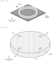
- the glass substrate 5 and the glass substrate 6 in Embodiment 2 are different from those in Embodiment 1 in that planar shapes thereof are circular. By using the circular glass substrate 5 and glass substrate 6, generation of unique stress can be prevented when a load is applied. Accordingly, in Embodiment 2, a structure in which a load distribution on the metal film 3 is uniform can be implemented, and high surface precision can be implemented.
- the bonding jig 200 in Embodiment 2 includes the restraint jig 80, the base plate 20, the lower fixing plate 30, the upper fixing plate 40, the load applying member 50, and a plurality of screws 60.
- the structure will be described with reference to FIG. 14 to FIG. 20 .
- FIG. 14 shows the restraint jig 80.
- the restraint jig 80 has a circular shape in plan view.
- the restraint jig 80 is made of, for example, copper.
- the restraint jig 80 has an opening 83 at a central portion thereof.
- the opening 83 has a circular planar shape.
- Step S26 described above is performed in a state where the restraint jig 80 is installed on the back surface BS2 of the metal film 3 around the transfer area 3a such that the transfer area 3a is located inside the opening 83 in plan view.
- the base plate 20, the lower fixing plate 30, the upper fixing plate 40, and the load applying member 50 have substantially the same structure as that of Embodiment 1 except that the planar shape thereof is mainly circular, and play the same role as that of Embodiment 1.
- the base plate 20 is not provided with the guide pins 22, and the lower fixing plate 30 and the upper fixing plate 40 are not provided with the holes 32 and the holes 42, but these members may be provided.
- the opening 33 of the lower fixing plate 30 has a circular planar shape. Accordingly, the circular glass substrate 6 can be fitted into the opening 33.
- the opening 43 of the upper fixing plate 40 has a circular planar shape. Accordingly, the circular glass substrate 5 can be fitted into the opening 43.
- FIG. 19 shows a process of installing the metal film 3 on the bonding jig 200
- FIG. 20 shows a state where the metal film 3 is installed on the bonding jig 200.
- the base plate 20, the lower fixing plate 30, the glass substrate 6, the metal film 3, and the restraint jigs 80 are prepared.
- the lower fixing plate 30 is provided on the base plate 20.
- the glass substrate 6 is provided inside the opening 33 of the lower fixing plate 30.
- the metal film 3 is installed on the glass substrate 6, and the metal film 3 around the transfer area 3a is provided on the lower fixing plate 30.
- the bonding agent 4 is provided on the back surface BS2 of the metal film 3.
- the restraint jig 80 is provided on the back surface BS2 of the metal film 3 around the transfer area 3a.
- the upper fixing plate 40, the glass substrate 5, the load applying member 50, and the screws 60 are prepared.
- the upper fixing plate 40 is installed on the restraint jig 80.
- the glass substrate 5 is installed inside the opening 43 of the upper fixing plate 40.
- the load applying member 50 is installed on the glass substrate 5.
- FIG. 21 and FIG. 22 are cross-sectional views taken along a line B-B shown in FIG. 20 .
- a step of bonding the back surface BS2 of the metal film 3 to the glass substrate 5 via the bonding agent 4 is performed. This step is performed in a vacuum atmosphere as in Embodiment 1.
- the metal film 3 is installed on the glass substrate 6 such that the front surface FS2 of the metal film 3 faces the glass substrate 6.
- the bonding agent 4 is provided on the back surface BS2 of the metal film 3.
- the glass substrate 5 is provided at a position physically separated from the back surface of the metal film 3. That is, the gap 70 is formed between the glass substrate 5 and the metal film 3 (the bonding agent 4).
- an installation surface of the glass substrate 6 on which the metal film 3 is installed and a bonding surface of the glass substrate 5 bonded to the metal film 3 via the bonding agent 4 are flat surfaces.
- Embodiment 2 substantially the same effect as that of Embodiment 1 can be obtained.
- the diffraction grating 7 manufactured in Embodiment 2 can also be applied as an optical element used in a spectrometer or the like as in Embodiment 1, and can be applied to manufacture of a plurality of replica gratings as a master diffraction grating as shown in FIG. 12 .
Landscapes
- Physics & Mathematics (AREA)
- Engineering & Computer Science (AREA)
- General Physics & Mathematics (AREA)
- Optics & Photonics (AREA)
- Manufacturing & Machinery (AREA)
- Microelectronics & Electronic Packaging (AREA)
- Diffracting Gratings Or Hologram Optical Elements (AREA)
Abstract
First, a wafer 1a having, on a front surface FS1 thereof, a pattern 1b having a shape in which concave portions and convex portions are alternately arranged is prepared. Next, a metal film 3 is formed on the front surface FS1 of the wafer 1a, and a transfer area 3a to which the shape of the pattern 1b is transferred is formed on a part of a front surface FS2 of the metal film 3. Next, the metal film 3 is removed from the wafer 1a. Next, a back surface BS2 of the metal film 3 is bonded to a glass substrate 5 via a bonding agent 4. In this way, a diffraction grating 7 is manufactured.
Description
- The present invention relates to a method for manufacturing a diffraction grating and a method for manufacturing a replica grating performed by using the diffraction grating as a mold.
- A diffraction grating is an optical element used in a spectrometer of an analysis device, or the like, and is used to separate light (white light) containing a mixture of various wavelengths into narrow-band wavelengths. Fine grooves are carved on a front surface of the diffraction grating, and a reflective film is deposited on the surfaces of the fine grooves.
- In related art, a method can be implemented in which a master diffraction grating is manufactured by marking grooves on a glass substrate coated with a metal film using a processing machine such as a ruling engine, and a replica grating is manufactured by transferring a groove shape marked in the master diffraction grating to a resin film or a metal film.
- In recent years, as a technique for manufacturing a diffraction grating, there is a method using holographic exposure using two-beam interference of a laser. In the method using holographic exposure, a diffraction grating is manufactured by performing holographic exposure on a photoresist coated on a silicon wafer.
- In recent years, a semiconductor manufacturing technique is also used as a technique for manufacturing a diffraction grating. For example,
PTL 1 discloses a technique for manufacturing a phase shift mask for manufacturing a diffraction grating by using an exposure device used for manufacturing a semiconductor and etching processing.PTL 1 discloses a technique in which a glass substrate is etched by high-density plasma etching using a resist pattern as a mask, and further wet etching is performed on the glass substrate to form an uneven shape on the glass substrate. -
PTL 2 discloses a method for manufacturing a sinusoidal optical grating by transferring an uneven shape formed on a resist to a glass substrate using an anisotropic dry etching method such as low-pressure high-density plasma etching. -
- PTL 1:
JP11-223714A - PTL 2:
JP2003-172639A - In the technique of the related art, high surface precision cannot be implemented since warpage of a silicon wafer is also transferred when an uneven shape formed on the silicon wafer is transferred to a resin film. In the methods using high-density plasma etching that are disclosed in
PTL 1 andPTL 2, it is difficult to prepare a silicon wafer or a glass substrate without warpage. - As a size of the silicon wafer increases, the warpage of the silicon wafer also increases, making it difficult to increase an area of the diffraction grating.
- On the other hand, in order to prevent the warpage of the silicon wafer, a method of transferring an uneven shape of a diffraction grating to a resin film by performing transfer with a load being applied to the silicon wafer is also studied. However, when a peripheral portion of the diffraction grating is a free end, a bonding agent for bonding the diffraction grating and the resin film contracts, and wrinkles are generated. Therefore, the high surface precision cannot be implemented.
- A main object of the present application is to provide a diffraction grating that has high surface precision and can be made large in area. Other problems and novel features will become apparent from the description of the present description and the accompanying drawings.
- A method for manufacturing a diffraction grating in one embodiment includes: a step (a) of preparing a wafer having, on a front surface thereof, a pattern having a shape in which concave portions and convex portions are alternately arranged; a step (b) of, after the step (a), forming a metal film on the front surface of the wafer and forming, on a part of the front surface of the metal film, a first transfer area to which the shape of the pattern is transferred; a step (c) of, after the step (b), removing the metal film from the wafer; and a step (d) of, after the step (c), bonding a back surface of the metal film to a first glass substrate via a bonding agent.
- According to one embodiment, a diffraction grating that has high surface precision and can be made large in area can be provided.
-
- [
FIG. 1] FIG. 1 is a cross-sectional view showing an outline of a method for manufacturing a diffraction grating inEmbodiment 1. - [
FIG. 2] FIG. 2 is a plan view showing a restraint jig inEmbodiment 1. - [
FIG. 3] FIG. 3 is a perspective view showing the restraint jig and a metal film inEmbodiment 1. - [
FIG. 4] FIG. 4 is a perspective view showing a base plate inEmbodiment 1. - [
FIG. 5] FIG. 5 is a perspective view showing a lower fixing plate inEmbodiment 1. - [
FIG. 6] FIG. 6 is a perspective view showing an upper fixing plate inEmbodiment 1. - [
FIG. 7] FIG. 7 is a perspective view showing a load applying plate inEmbodiment 1. - [
FIG. 8] FIG. 8 is a perspective view showing a process of installing the metal film on a bonding jig in Embodiment 1. - [
FIG. 9] FIG. 9 is a perspective view showing a state where the metal film is installed on the bonding jig in Embodiment 1. - [
FIG. 10] FIG. 10 is a cross-sectional view showing a state where the metal film is installed on the bonding jig in Embodiment 1. - [
FIG. 11] FIG. 11 is a cross-sectional view showing a state where the metal film is installed on the bonding jig in Embodiment 1. - [
FIG. 12] FIG. 12 is a cross-sectional view showing an outline of a method for manufacturing a replica grating inEmbodiment 1. - [
FIG. 13] FIG. 13 is a cross-sectional view showing an outline of a method for manufacturing a diffraction grating inEmbodiment 2. - [
FIG. 14] FIG. 14 is a perspective view showing a restraint jig and a metal film inEmbodiment 2. - [
FIG. 15] FIG. 15 is a perspective view showing a base plate inEmbodiment 2. - [
FIG. 16] FIG. 16 is a perspective view showing a lower fixing plate inEmbodiment 2. - [
FIG. 17] FIG. 17 is a perspective view showing an upper fixing plate inEmbodiment 2. - [
FIG. 18] FIG. 18 is a perspective view showing a load applying plate inEmbodiment 2. - [
FIG. 19] FIG. 19 is a perspective view showing a process of installing the metal film on the bonding jig in Embodiment 2. - [
FIG. 20] FIG. 20 is a perspective view showing a state where the metal film is installed on the bonding jig in Embodiment 2. - [
FIG. 21] FIG. 21 is a cross-sectional view showing a state where the metal film is installed on the bonding jig in Embodiment 2. - [
FIG. 22] FIG. 22 is a cross-sectional view showing a state where the metal film is installed on the bonding jig in Embodiment 2. - Hereinafter, embodiments will be described in detail with reference to the drawings. In all the drawings for describing the embodiments, members having the same functions are denoted by the same reference numerals, and a repeated description thereof is omitted. In the following embodiments, the description of the same or similar parts will not be repeated in principle except when necessary.
- An X direction, a Y direction, and a Z direction described in the present application intersect each other and are orthogonal to each other. In the present application, the Z direction is described as a longitudinal direction, an up-down direction, a height direction, or a thickness direction of a structure. The expression "plan view" used in the present application means viewing a plane formed by the X direction and the Y direction from the Z direction, and the expression "planar shape" means the above-described shape in plan view.
- A method for manufacturing a diffraction grating in
Embodiment 1 will be described below with reference toFIG. 1 . The method for manufacturing a diffraction grating inEmbodiment 1 includes steps S11 to S18 shown inFIG. 1 . - In step S11, a silicon diffraction grating 1 is prepared. The
silicon diffraction grating 1 includes awafer 1a made of, for example, silicon and having a front surface FS1 and a back surface BS1. Thewafer 1a has, on the front surface FS1 thereof, apattern 1b having a shape in which concave portions and convex portions are alternately arranged. - The
pattern 1b is, for example, a resist pattern formed by a photolithography technique used in the field of manufacturing a semiconductor or a holographic exposure technique using interference of laser light. More specifically, thepattern 1b has a sinusoidal shape, a rectangular shape, a triangular shape, or a blazed shape. An area where thepattern 1b is formed (a marked line area) has a square planar shape, a rectangular planar shape, or a circular planar shape. - In steps S12 and S13, a
metal film 3 is formed on the front surface FS1 of thewafer 1a, and atransfer area 3a to which the shape of thepattern 1b is transferred is formed on a part of a front surface FS2 of themetal film 3. - First, in step S12, a
seed film 2 is deposited on the front surface FS1 of thewafer 1a having thepattern 1b by, for example, a sputtering method. Theseed film 2 is made of a conductive material such as chromium, titanium, platinum, or gold. However, the material constituting theseed film 2 is not limited to the above-described material, and it is sufficient that the material has a function of carrying electrons from an electrode disposed on an end portion of thewafer 1a to a center of thewafer 1a without a voltage drop during electrolytic plating. - Next, in step S13, the
metal film 3 is formed on the front surface FS1 of thewafer 1a (on the seed film 2) by, for example, a plating method so as to fill the concave portions of thepattern 1b and cover the convex portions of thepattern 1b. As the above-described plating method, an electrolytic plating method is suitable. Themetal film 3 is made of a conductive material such as nickel or copper. However, the material constituting themetal film 3 is not limited to the above-described material, and any material may be used as long as electrolytic plating is possible and a film can be formed along the shape of thepattern 1b with high accuracy. In the following drawings, illustration of theseed film 2 is omitted. - In step S14, the
metal film 3 is removed from thewafer 1a. Themetal film 3 has the front surface FS2 and a back surface BS2. Thetransfer area 3a to which the shape of thepattern 1b is transferred is formed on a part of the front surface FS2. That is, thetransfer area 3a has a shape in which concave portions and convex portions are alternately arranged, and has a sinusoidal shape, a rectangular shape, a triangular shape, or a blazed shape. The back surface BS2 is a flat surface. - In step S15, a
bonding agent 4 is provided on the back surface BS2 of themetal film 3. Thebonding agent 4 is applied to the back surface BS2 by, for example, a coating method, and is made of a material capable of bonding themetal film 3 and aglass substrate 5 to be described later without requiring a heat treatment. Since there is a large difference in linear expansion coefficient between the metal and the glass, the material constituting thebonding agent 4 is preferably a material that does not require a heat treatment. - In step S16, the
metal film 3 is fixed by sandwiching an outer periphery of themetal film 3 between tworestraint jigs 10 at a position not overlapping thetransfer area 3a. - In step S17, the
glass substrate 5 is bonded to themetal film 3 in abonding jig 100 to be described later. Theglass substrate 5 is provided on a front surface FS2 side of themetal film 3, and aglass substrate 6 is provided on a back surface BS2 side of themetal film 3. Thereafter, theglass substrate 5 is pressed toward the back surface BS2, and themetal film 3 is bonded to theglass substrate 5 via thebonding agent 4. - In step S18, the
glass substrate 5 and themetal film 3 that are bonded to each other are taken out from thebonding jig 100. By such a manufacturing method, a diffraction grating (glass diffraction grating) 7 including theglass substrate 5, thebonding agent 4, and themetal film 3 is manufactured. - As described above, although the
restraint jig 10 is used in step S16 and subsequent steps, thebonding jig 100 including therestraint jig 10 can be prepared in advance, and step S16 and subsequent steps are performed using thebonding jig 100. Hereinafter, each member of thebonding jig 100 and the method for manufacturing a diffraction grating in step S16 and subsequent steps will be described in detail with reference toFIGS. 2 to 11 . - As shown in
FIG. 9 , thebonding jig 100 inEmbodiment 1 includes two restraint jigs 10, abase plate 20, alower fixing plate 30, anupper fixing plate 40, aload applying member 50, and a plurality ofscrews 60. Hereinafter, the structure will be described with reference toFIG. 2 to FIG. 7 . -
FIG. 2 andFIG. 3 show therestraint jig 10. Therestraint jig 10 has a polygonal shape in plan view, and here, has a square shape. Therestraint jig 10 is made of a material having high strength and high heat resistance, for example, stainless steel. Therestraint jig 10 has anopening 13 in a central portion thereof, and has a plurality ofholes 11 and a plurality ofholes 12 around theopening 13. Theholes 11 are provided for fixing to other members withscrews 60, and theholes 12 are provided for aligning with guide pins 22 of thebase plate 20. - The
metal film 3 has a polygonal planar shape, here, has a square planar shape. Theopening 13 has a polygonal planar shape corresponding to the planar shape of themetal film 3, here, has a square planar shape. Ahole 14 integrated with theopening 13 is provided at each corner of theopening 13. In other words, therestraint jig 10 has a plurality ofholes 14, and each of the plurality ofholes 14 encloses each corner of theopening 13. - Step S16 described above is performed in a state where the
metal film 3 around thetransfer area 3a is sandwiched between two restraint jigs such that thetransfer area 3a is located inside theopening 13 in plan view. At this time, each corner of themetal film 3 is located inside thehole 14 in plan view. In step S17, themetal film 3 is pressed against theglass substrate 5, and each corner of themetal film 3 is a portion where stress is easily concentrated. Therefore, unique stress is often generated at each corner. Here, by positioning each corner of themetal film 3 inside thehole 14, the concentration of stress at each corner can be alleviated, and a structure in which a load distribution on themetal film 3 is uniform can be implemented. -
FIG. 4 shows thebase plate 20. Thebase plate 20 has a planar shape similar to that of therestraint jig 10. A plurality ofholes 21 and the guide pins 22 are provided in an outer peripheral portion of thebase plate 20. Theholes 21 are provided for fixing to other members with thescrews 60, and the guide pins 22 are provided for aligning with other members. -
FIG. 5 shows thelower fixing plate 30. Thelower fixing plate 30 has a planar shape similar to that of therestraint jig 10. Thelower fixing plate 30 has anopening 33 at a central portion thereof, and has a plurality ofholes 31 and a plurality ofholes 32 around theopening 33. Theholes 31 are provided for fixing to other members withscrews 60, and theholes 32 are provided for aligning with the guide pins 22 of thebase plate 20. - The
lower fixing plate 30 is a member for fixing a position of theglass substrate 6, and has theopening 33. Theopening 33 and theglass substrate 6 each have a polygonal planar shape, here, have a square planar shape. Accordingly, theglass substrate 6 is fitted into theopening 33. -
FIG. 6 shows theupper fixing plate 40. Theupper fixing plate 40 has a planar shape similar to that of therestraint jig 10. Theupper fixing plate 40 has anopening 43 at a central portion thereof, and has a plurality ofholes 41 and a plurality ofholes 42 around theopening 43. Theholes 41 are provided for fixing to other members with thescrews 60, and theholes 42 are provided for aligning with the guide pins 22 of thebase plate 20. - The
upper fixing plate 40 is a member for fixing a position of theglass substrate 5, and has theopening 43. Theopening 43 and theglass substrate 5 each have a polygonal planar shape, here, have a square planar shape. Accordingly, theglass substrate 5 is fitted into theopening 43. -
FIG. 7 shows theload applying member 50. Theload applying member 50 is used when applying a load to theglass substrate 5. Theload applying member 50 has a polygonal planar shape, here, has a square planar shape. Theload applying member 50 is designed to be accommodated in theopening 43 of theupper fixing plate 40. - The
base plate 20, thelower fixing plate 30, theupper fixing plate 40, and theload applying member 50 are made of a material having high strength and high heat resistance, for example, stainless steel. -
FIG. 8 shows a process of installing themetal film 3 on thebonding jig 100, andFIG. 9 shows a state where themetal film 3 is installed on thebonding jig 100. - As shown in
FIG. 8 , thebase plate 20, thelower fixing plate 30, theglass substrate 6, themetal film 3, and tworestraint jigs 10 are prepared. First, thelower fixing plate 30 is provided on thebase plate 20 while fitting the guide pins 22 of thebase plate 20 into theholes 32. Next, theglass substrate 6 is provided inside theopening 33 of thelower fixing plate 30. - Next, the
first restraint jig 10 is installed on thelower fixing plate 30 while fitting theholes 12 into the guide pins 22 of thebase plate 20. Next, themetal film 3 is installed on theglass substrate 6, and themetal film 3 around thetransfer area 3a is provided on thefirst restraint jig 10. Thebonding agent 4 is provided on the back surface BS2 of themetal film 3. Next, thesecond restraint jig 10 is provided on the back surface BS2 of themetal film 3 around thetransfer area 3a while fitting the guide pins 22 of thebase plate 20 into theholes 12 of theupper fixing plate 40. - Next, as shown in
FIG. 9 , theupper fixing plate 40, theglass substrate 5, theload applying member 50, and thescrews 60 are prepared. Theupper fixing plate 40 is installed on thesecond restraint jig 10 while fitting the guide pins 22 of thebase plate 20 into theholes 42. Next, theglass substrate 5 is installed inside theopening 43 of theupper fixing plate 40. Next, theload applying member 50 is installed on theglass substrate 5. - Thereafter, positions thereof are fixed by inserting the
screws 60 into theholes 41 of theupper fixing plate 40, theholes 11 of the two restraint jigs 10, theholes 31 of thelower fixing plate 30, and theholes 21 of thebase plate 20. Accordingly, themetal film 3 is fixed in a state where themetal film 3 around thetransfer area 3a is sandwiched between the two restraint jigs. - Hereinafter, a state before and after a load is applied to the
metal film 3 will be described with reference toFIGS. 10 and 11. FIG. 10 and FIG. 11 are cross-sectional views taken along a line A-A shown inFIG. 9 . - By shifting a state of "before load application" shown in
FIG. 10 to a state of "after load application" shown inFIG. 11 , a step of bonding the back surface BS2 of themetal film 3 to theglass substrate 5 via thebonding agent 4 is performed. This step is performed in a vacuum atmosphere. - First, in
FIG. 10 , themetal film 3 is installed on theglass substrate 6 such that the front surface FS2 of themetal film 3 faces theglass substrate 6. Thebonding agent 4 is provided on the back surface BS2 of themetal film 3. Theglass substrate 5 is provided at a position physically separated from the back surface of themetal film 3. That is, agap 70 is formed between theglass substrate 5 and the metal film 3 (the bonding agent 4). An installation surface of theglass substrate 6 on which themetal film 3 is installed and a bonding surface of theglass substrate 5 bonded to themetal film 3 via thebonding agent 4 are flat surfaces. - From such a state, by pressing the
glass substrate 5 toward the back surface BS2 of themetal film 3 by theload applying member 50, a state as shown inFIG. 11 is obtained. The "after load application" corresponds to step S17 inFIG. 1 . Thereafter, by dismantling thebonding jig 100, adiffraction grating 7 including theglass substrate 5 and themetal film 3 that are bonded via thebonding agent 4 can be obtained. - As described above, according to the method for manufacturing a diffraction grating in
Embodiment 1, the shape of thepattern 1b provided on thewafer 1a is transferred to themetal film 3, and themetal film 3 is used for thediffraction grating 7. Accordingly, warpage of the silicon wafer, which is a problem in the related art, can be prevented from being transferred, and thus thediffraction grating 7 that has high surface precision and can be made large in area can be provided. - On the other hand, according to the study of the present inventors, when bonding the
glass substrate 5 and themetal film 3 via thebonding agent 4, thebonding agent 4 contracts, themetal film 3 is drawn in, and wrinkles are generated. In a case where the bonding step is performed in the atmosphere, wrinkles are generated when air bubbles are mixed, making it difficult to achieve high surface precision. - In contrast, in
Embodiment 1, theglass substrate 5 is pressed while the outer periphery of themetal film 3 is fixed by the restraint jigs 10. Accordingly, the generation of wrinkles due to the influence of the contraction of thebonding agent 4 can be prevented. Since thebonding agent 4 is made of a material that does not require a heat treatment, the influence of contraction of thebonding agent 4 can be prevented. - The back surface BS2 of the
metal film 3 and the bonding surface of theglass substrate 5 that are bonded via thebonding agent 4 are flat surfaces. Here, when theglass substrate 5 is simply pressed against the back surface BS2 of themetal film 3, air bubbles are mixed and wrinkles are easily generated. Therefore, as shown inFIG. 10 , thegap 70 is provided between theglass substrate 5 and the metal film 3 (the bonding agent 4). By pressing theglass substrate 5 against the back surface BS2 of themetal film 3 in a vacuum atmosphere, the back surface BS2 of themetal film 3 and theglass substrate 5 are bonded via thebonding agent 4. Accordingly, the generation of wrinkles due to air bubbles can be prevented, and the high surface precision can be implemented. - The
diffraction grating 7 manufactured inEmbodiment 1 can be applied as an optical element used in a spectrometer or the like. For example, a step of forming a reflective film made of a material having a light reflectivity higher than that of the material constituting themetal film 3 on the front surface FS2 of themetal film 3 including thetransfer area 3a is added between step S14 and step S15 inFIG. 1 . Such a reflective film is, for example, an aluminum film, and can be formed by, for example, a vapor deposition method. Accordingly, thediffraction grating 7 can be used as a reflective optical element. -
FIG. 12 is another application example of thediffraction grating 7, and shows a method for manufacturing a replica grating performed by using thediffraction grating 7 as a mold. That is,FIG. 12 shows a method for manufacturing a plurality of replica gratings by using thediffraction grating 7 as a master diffraction grating. - First, in step S31, a
resin film 91 having a front surface FS3 and a back surface BS3 and aglass substrate 92 bonded to the back surface BS3 of theresin film 91 are prepared. Theresin film 91 is a thermosetting resin such as an epoxy resin. - In step S32, the
diffraction grating 7 is prepared, and a peripheral portion of themetal film 3 is cut in accordance with a size of theglass substrate 5. - In step S33, the
resin film 91 is pressed onto the front surface FS2 of themetal film 3 including thetransfer area 3a. Accordingly, atransfer area 91a to which a shape of thetransfer area 3a is transferred is formed on a part of the front surface FS3 of theresin film 91. That is, thetransfer area 91a has a shape in which concave portions and convex portions are alternately arranged, and has a sinusoidal shape, a rectangular shape, a triangular shape, or a blazed shape. Next, theresin film 91 is cured in a state where the shape of thetransfer area 91a is maintained by performing a heat treatment of, for example, 70 °C to 150 °C on theresin film 91. - In step S34, the
resin film 91 and theglass substrate 92 are removed from themetal film 3. Accordingly, a replica grating 93 having theresin film 91 including thetransfer area 91a and theglass substrate 92 is manufactured. By repeating such steps S31 to S33, a plurality ofreplica gratings 93 can be easily manufactured based on thediffraction grating 7. - As described above, in the
diffraction grating 7 including themetal film 3, the warpage of thewafer 1a is prevented from being transferred, and high surface precision is implemented. Accordingly, even in the replica grating 93 including theglass substrate 92 and theresin film 91 including thetransfer area 91a to which the shape of thetransfer area 3a is transferred, the warpage of thewafer 1a is prevented from being transferred, and the high surface precision is implemented. - When the replica grating 93 is applied as a reflective optical element, a reflective film is formed on the front surface FS3 of the
resin film 91 including thetransfer area 91a. Such a reflective film is, for example, an aluminum film, and can be formed by, for example, a vapor deposition method. - A method for manufacturing a diffraction grating in
Embodiment 2 will be described below with reference toFIG. 13 . The method for manufacturing a diffraction grating inEmbodiment 2 includes steps S21 to S28 shown inFIG. 13 . In the following description, differences fromEmbodiment 1 will be mainly described, and overlapping points withEmbodiment 1 will not be described. - Steps S21 to S25 are the same as steps S11 to S15 in
Embodiment 1. In step S26, an outer periphery of themetal film 3 is fixed at a position not overlapping thetransfer area 3a by using arestraint jig 80. - In step S27, the
glass substrate 5 is bonded to themetal film 3 in abonding jig 200 to be described later. Theglass substrate 5 is provided on a front surface FS2 side of themetal film 3, and theglass substrate 6 is provided on a back surface BS2 side of themetal film 3. Thereafter, theglass substrate 5 is pressed toward the back surface BS2, and themetal film 3 is bonded to theglass substrate 5 via thebonding agent 4. - In step S28, the
glass substrate 5 and themetal film 3 that are bonded to each other are taken out from thebonding jig 100. As described above, thediffraction grating 7 including theglass substrate 5, thebonding agent 4, and themetal film 3 is manufactured as the diffraction grating inEmbodiment 1. - The
glass substrate 5 and theglass substrate 6 inEmbodiment 2 are different from those inEmbodiment 1 in that planar shapes thereof are circular. By using thecircular glass substrate 5 andglass substrate 6, generation of unique stress can be prevented when a load is applied. Accordingly, inEmbodiment 2, a structure in which a load distribution on themetal film 3 is uniform can be implemented, and high surface precision can be implemented. - Hereinafter, each member of the
bonding jig 200 and the method for manufacturing a diffraction grating in step S26 and subsequent steps will be described in detail with reference toFIG. 14 to FIG. 22 . - As shown in
FIG. 20 , thebonding jig 200 inEmbodiment 2 includes therestraint jig 80, thebase plate 20, thelower fixing plate 30, theupper fixing plate 40, theload applying member 50, and a plurality ofscrews 60. Hereinafter, the structure will be described with reference toFIG. 14 to FIG. 20 . -
FIG. 14 shows therestraint jig 80. Therestraint jig 80 has a circular shape in plan view. Therestraint jig 80 is made of, for example, copper. Therestraint jig 80 has anopening 83 at a central portion thereof. Theopening 83 has a circular planar shape. - Step S26 described above is performed in a state where the
restraint jig 80 is installed on the back surface BS2 of themetal film 3 around thetransfer area 3a such that thetransfer area 3a is located inside theopening 83 in plan view. - As shown in
FIG. 15 to FIG. 18 , thebase plate 20, thelower fixing plate 30, theupper fixing plate 40, and theload applying member 50 have substantially the same structure as that ofEmbodiment 1 except that the planar shape thereof is mainly circular, and play the same role as that ofEmbodiment 1. InEmbodiment 2, thebase plate 20 is not provided with the guide pins 22, and thelower fixing plate 30 and theupper fixing plate 40 are not provided with theholes 32 and theholes 42, but these members may be provided. - As shown in
FIG. 16 , theopening 33 of thelower fixing plate 30 has a circular planar shape. Accordingly, thecircular glass substrate 6 can be fitted into theopening 33. As shown inFIG. 17 , theopening 43 of theupper fixing plate 40 has a circular planar shape. Accordingly, thecircular glass substrate 5 can be fitted into theopening 43. -
FIG. 19 shows a process of installing themetal film 3 on thebonding jig 200, andFIG. 20 shows a state where themetal film 3 is installed on thebonding jig 200. - As shown in
FIG. 19 , thebase plate 20, thelower fixing plate 30, theglass substrate 6, themetal film 3, and the restraint jigs 80 are prepared. First, thelower fixing plate 30 is provided on thebase plate 20. Next, theglass substrate 6 is provided inside theopening 33 of thelower fixing plate 30. Next, themetal film 3 is installed on theglass substrate 6, and themetal film 3 around thetransfer area 3a is provided on thelower fixing plate 30. Thebonding agent 4 is provided on the back surface BS2 of themetal film 3. Next, therestraint jig 80 is provided on the back surface BS2 of themetal film 3 around thetransfer area 3a. - Next, as shown in
FIG. 20 , theupper fixing plate 40, theglass substrate 5, theload applying member 50, and thescrews 60 are prepared. Theupper fixing plate 40 is installed on therestraint jig 80. Next, theglass substrate 5 is installed inside theopening 43 of theupper fixing plate 40. Next, theload applying member 50 is installed on theglass substrate 5. - Thereafter, positions thereof are fixed by inserting the
screws 60 into theholes 41 of theupper fixing plate 40, theholes 31 of thelower fixing plate 30, and theholes 21 of thebase plate 20. Accordingly, themetal film 3 around thetransfer area 3a can be fixed between therestraint jig 80 and thelower fixing plate 30. InEmbodiment 2, when theupper fixing plate 40 is fixed with thescrews 60, therestraint jig 80 may be compressed by theupper fixing plate 40. As long as themetal film 3 can be fixed, there is no particular problem even when therestraint jig 80 is compressed. - Hereinafter, states before and after a load is applied to the
metal film 3 will be described with reference toFIG. 21 and FIG. 22. FIG. 21 and FIG. 22 are cross-sectional views taken along a line B-B shown inFIG. 20 . - By shifting a state of "before load application" shown in
FIG. 21 to a state of "after load application" shown inFIG. 22 , a step of bonding the back surface BS2 of themetal film 3 to theglass substrate 5 via thebonding agent 4 is performed. This step is performed in a vacuum atmosphere as inEmbodiment 1. - First, in
FIG. 21 , themetal film 3 is installed on theglass substrate 6 such that the front surface FS2 of themetal film 3 faces theglass substrate 6. Thebonding agent 4 is provided on the back surface BS2 of themetal film 3. Theglass substrate 5 is provided at a position physically separated from the back surface of themetal film 3. That is, thegap 70 is formed between theglass substrate 5 and the metal film 3 (the bonding agent 4). InEmbodiment 2, an installation surface of theglass substrate 6 on which themetal film 3 is installed and a bonding surface of theglass substrate 5 bonded to themetal film 3 via thebonding agent 4 are flat surfaces. - From such a state, by pressing the
glass substrate 5 toward the back surface BS2 of themetal film 3 by theload applying member 50, a state as shown inFIG. 22 is obtained. The "after load application" corresponds to step S27 inFIG. 13 . Thereafter, by dismantling thebonding jig 200, thediffraction grating 7 including theglass substrate 5 and themetal film 3 that are bonded via thebonding agent 4 can be obtained. - In this way, according to
Embodiment 2, substantially the same effect as that ofEmbodiment 1 can be obtained. Thediffraction grating 7 manufactured inEmbodiment 2 can also be applied as an optical element used in a spectrometer or the like as inEmbodiment 1, and can be applied to manufacture of a plurality of replica gratings as a master diffraction grating as shown inFIG. 12 . - Although the present invention has been specifically described based on the above-described embodiments, the present invention is not limited to the above-described embodiments, and various modifications can be made without departing from the gist of the present invention.
-
- 1: silicon diffraction grating
- 1a: wafer
- 1b: pattern
- 2: seed film
- 3: metal film
- 3a: transfer area
- 4: bonding agent
- 5, 6: glass substrate
- 7: diffraction grating (glass diffraction grating)
- 10: restraint jig
- 11: hole for fixing
- 12: hole for aligning
- 13: opening
- 14: hole
- 20: base plate
- 21: hole for fixing
- 22: guide pin
- 30: lower fixing plate for glass substrate
- 31: hole for fixing
- 32: hole for aligning
- 33: opening
- 40: upper fixing plate for glass substrate
- 41: hole for fixing
- 42: hole for aligning
- 43: opening
- 50: load applying member
- 60: screw
- 70: gap
- 80: restraint jig
- 83: opening
- 91: resin film
- 91a: transfer area
- 92: glass substrate
- 93: replica grating
- 100, 200: bonding jig
- FS1: front surface of wafer
- FS2: front surface of metal film
- FS3: front surface of resin film
- BS1: back surface of wafer
- BS2: back surface of metal film
- BS3: back surface of resin film
Claims (12)
- A method for manufacturing a diffraction grating, the method comprising:a step (a) of preparing a wafer having, on a front surface thereof, a pattern having a shape in which concave portions and convex portions are alternately arranged;a step (b) of, after the step (a), forming a metal film on the front surface of the wafer and forming, on a part of a front surface of the metal film, a first transfer area to which the shape of the pattern is transferred;a step (c) of, after the step (b), removing the metal film from the wafer; anda step (d) of, after the step (c), bonding a back surface of the metal film to a first glass substrate via a bonding agent.
- The method for manufacturing a diffraction grating according to claim 1, further comprising:a step (e) of preparing a first restraint jig having a first opening in a central portion thereof and a second restraint jig having a second opening in a central portion thereof, whereinthe step (d) is performed in a state where the metal film around the first transfer area is sandwiched between the first restraint jig and the second restraint jig such that the first transfer area is located inside each of the first opening and the second opening in plan view.
- The method for manufacturing a diffraction grating according to claim 2, further comprising:a step (f) of preparing a load applying member for applying a load to the first glass substrate, whereinthe step (d) is performed by pressing the first glass substrate toward the back surface of the metal film by the load applying member from a state where the bonding agent is provided on the back surface of the metal film and the first glass substrate is provided at a position physically separated from the back surface of the metal film.
- The method for manufacturing a diffraction grating according to claim 2, whereinthe first opening and the second opening each have a polygonal planar shape,each corner of the first opening and each corner of the second opening are provided with a hole integrated with the first opening and a hole integrated with the second opening, respectively,the metal film has a polygonal planar shape, andin the step (d), each corner of the metal film is located inside the hole of each of the first opening and the second opening in plan view.
- The method for manufacturing a diffraction grating according to claim 1, further comprising:a step (g) of preparing a third restraint jig having a circular shape in plan view and having a third opening that is circular in plan view in a central portion thereof, whereinthe step (d) is performed in a state where the third restraint jig is installed on the back surface of the metal film around the first transfer area such that the first transfer area is located inside the third opening in plan view.
- The method for manufacturing a diffraction grating according to claim 5, further comprising:a step (h) of preparing a first fixing plate having a fourth opening that is circular in plan view in a central portion thereof, a second glass substrate that is circular in plan view, and a load applying member for applying a load to the first glass substrate, whereinthe second glass substrate is provided inside the fourth opening,the metal film around the first transfer area is fixed between the third restraint jig and the first fixing plate, andthe step (d) is performed by pressing the first glass substrate toward the back surface of the metal film by the load applying member from a state where the metal film is installed on the second glass substrate such that the front surface of the metal film faces the second glass substrate, the bonding agent is provided on the back surface of the metal film, and the first glass substrate is provided at a position physically separated from the back surface of the metal film.
- The method for manufacturing a diffraction grating according to claim 1, whereinthe step (d) is performed in a vacuum atmosphere, andthe back surface of the metal film and a bonding surface of the first glass substrate that are bonded via the bonding agent are flat surfaces.
- The method for manufacturing a diffraction grating according to claim 1, wherein
in the step (b), the metal film is formed on the front surface of the wafer by a plating method so as to fill the concave portions of the pattern and cover the convex portions of the pattern. - The method for manufacturing a diffraction grating according to claim 1, wherein
the bonding agent is made of a material capable of bonding the metal film and the first glass substrate without requiring a heat treatment. - The method for manufacturing a diffraction grating according to claim 1, wherein
the pattern has a sinusoidal shape, a rectangular shape, a triangular shape, or a blazed shape. - The method for manufacturing a diffraction grating according to claim 1, further comprising:
a step (h) of forming a first reflective film on the front surface of the metal film including the first transfer area between the step (b) and the step (c), the first reflective film being made of a material having a light reflectivity higher than that of a material constituting the metal film. - A method for manufacturing a replica grating by using, as a mold, a diffraction grating manufactured by the method for manufacturing a diffraction grating according to claim 1 and including the first glass substrate and the metal film that are bonded via the bonding agent, the method comprising:a step (i) of preparing a resin film and a third glass substrate bonded to a back surface of the resin film;a step (j) of, after the step (i), pressing the resin film onto a front surface of the metal film including the first transfer area to form, on a part of a front surface of the resin film, a second transfer area to which a shape of the first transfer area is transferred; anda step (k) of removing the resin film and the third glass substrate from the metal film after the step (j).
Applications Claiming Priority (2)
| Application Number | Priority Date | Filing Date | Title |
|---|---|---|---|
| JP2021111419 | 2021-07-05 | ||
| PCT/JP2022/022546 WO2023281950A1 (en) | 2021-07-05 | 2022-06-02 | Method for manufacturing diffraction lattice and method for manufacturing replica diffraction lattice |
Publications (1)
| Publication Number | Publication Date |
|---|---|
| EP4369063A1 true EP4369063A1 (en) | 2024-05-15 |
Family
ID=84800612
Family Applications (1)
| Application Number | Title | Priority Date | Filing Date |
|---|---|---|---|
| EP22835555.8A Pending EP4369063A1 (en) | 2021-07-05 | 2022-06-02 | Method for manufacturing diffraction lattice and method for manufacturing replica diffraction lattice |
Country Status (4)
| Country | Link |
|---|---|
| EP (1) | EP4369063A1 (en) |
| JP (1) | JPWO2023281950A1 (en) |
| CN (1) | CN117501156A (en) |
| WO (1) | WO2023281950A1 (en) |
Family Cites Families (3)
| Publication number | Priority date | Publication date | Assignee | Title |
|---|---|---|---|---|
| JP6029502B2 (en) * | 2013-03-19 | 2016-11-24 | 株式会社日立ハイテクノロジーズ | Method for manufacturing curved diffraction grating |
| EP3745166B1 (en) * | 2017-12-27 | 2023-08-09 | Hitachi High-Tech Corporation | Manufacturing method of concave diffrraction grating |
| CN113167944A (en) * | 2018-07-23 | 2021-07-23 | 株式会社日立高新技术 | Method and apparatus for manufacturing concave diffraction grating, and concave diffraction grating |
-
2022
- 2022-06-02 EP EP22835555.8A patent/EP4369063A1/en active Pending
- 2022-06-02 WO PCT/JP2022/022546 patent/WO2023281950A1/en active Application Filing
- 2022-06-02 JP JP2023533470A patent/JPWO2023281950A1/ja active Pending
- 2022-06-02 CN CN202280042297.0A patent/CN117501156A/en active Pending
Also Published As
| Publication number | Publication date |
|---|---|
| CN117501156A (en) | 2024-02-02 |
| JPWO2023281950A1 (en) | 2023-01-12 |
| WO2023281950A1 (en) | 2023-01-12 |
Similar Documents
| Publication | Publication Date | Title |
|---|---|---|
| CN111095043B (en) | Method for manufacturing concave diffraction grating, and analyzer using same | |
| GB2509536A (en) | Diffraction grating | |
| CN102360092A (en) | Optical element and method for manufacturing the same | |
| EP4369063A1 (en) | Method for manufacturing diffraction lattice and method for manufacturing replica diffraction lattice | |
| US7501035B2 (en) | Method of manufacturing replica diffraction grating | |
| JP7348182B2 (en) | Concave diffraction grating manufacturing method, manufacturing device, and concave diffraction grating | |
| JP3675314B2 (en) | Diffraction grating | |
| US6379777B1 (en) | Die and production method thereof, glass substrate and production method thereof and method of forming pattern on the glass substrate | |
| JPH07261010A (en) | Replica diffraction grating | |
| US11366255B2 (en) | Concave diffraction grating, method for producing the same, and optical device | |
| KR102267128B1 (en) | Manufacturing method of encoder | |
| JP2021106285A (en) | Template for nanoimprint and method of manufacturing integrated circuit device | |
| KR100455088B1 (en) | Production method of lightwave guide | |
| JP7301201B2 (en) | Manufacturing method of concave diffraction grating | |
| JP7491747B2 (en) | Method for manufacturing concave diffraction grating | |
| US11333835B2 (en) | Microfabrication method for optical components | |
| JP4306212B2 (en) | Optical waveguide core manufacturing method | |
| JP2021150629A (en) | Method for manufacturing template, template and method for manufacturing semiconductor device | |
| TWI644135B (en) | Optical demultiplexing device and method of manufacturing same | |
| JP2004218002A (en) | Method for producing precise metallic member utilizing stripped surface from base material | |
| CN116848438A (en) | Forming an optical system | |
| US7609805B2 (en) | Mask used for LIGA process, method of manufacturing the mask, and method of manufacturing microstructure using LIGA process | |
| JPH0831827A (en) | Production process of microparts using substrate | |
| JPS63253304A (en) | Preparation of optical demultiplexer/multiplexer | |
| KR20170033453A (en) | Fabrication of X-ray with beam tunnel |
Legal Events
| Date | Code | Title | Description |
|---|---|---|---|
| STAA | Information on the status of an ep patent application or granted ep patent |
Free format text: STATUS: THE INTERNATIONAL PUBLICATION HAS BEEN MADE |
|
| PUAI | Public reference made under article 153(3) epc to a published international application that has entered the european phase |
Free format text: ORIGINAL CODE: 0009012 |
|
| STAA | Information on the status of an ep patent application or granted ep patent |
Free format text: STATUS: REQUEST FOR EXAMINATION WAS MADE |
|
| 17P | Request for examination filed |
Effective date: 20231214 |
|
| AK | Designated contracting states |
Kind code of ref document: A1 Designated state(s): AL AT BE BG CH CY CZ DE DK EE ES FI FR GB GR HR HU IE IS IT LI LT LU LV MC MK MT NL NO PL PT RO RS SE SI SK SM TR |