EP4369007B1 - System zur charakterisierung einer transistorschaltung - Google Patents
System zur charakterisierung einer transistorschaltung Download PDFInfo
- Publication number
- EP4369007B1 EP4369007B1 EP23201304.5A EP23201304A EP4369007B1 EP 4369007 B1 EP4369007 B1 EP 4369007B1 EP 23201304 A EP23201304 A EP 23201304A EP 4369007 B1 EP4369007 B1 EP 4369007B1
- Authority
- EP
- European Patent Office
- Prior art keywords
- voltage
- transistor
- transistor circuit
- gate
- predefined
- Prior art date
- Legal status (The legal status is an assumption and is not a legal conclusion. Google has not performed a legal analysis and makes no representation as to the accuracy of the status listed.)
- Active
Links
Images


Classifications
-
- G—PHYSICS
- G01—MEASURING; TESTING
- G01R—MEASURING ELECTRIC VARIABLES; MEASURING MAGNETIC VARIABLES
- G01R31/00—Arrangements for testing electric properties; Arrangements for locating electric faults; Arrangements for electrical testing characterised by what is being tested not provided for elsewhere
- G01R31/28—Testing of electronic circuits, e.g. by signal tracer
- G01R31/2851—Testing of integrated circuits [IC]
- G01R31/2855—Environmental, reliability or burn-in testing
- G01R31/2872—Environmental, reliability or burn-in testing related to electrical or environmental aspects, e.g. temperature, humidity, vibration, nuclear radiation
- G01R31/2879—Environmental, reliability or burn-in testing related to electrical or environmental aspects, e.g. temperature, humidity, vibration, nuclear radiation related to electrical aspects, e.g. to voltage or current supply or stimuli or to electrical loads
-
- H—ELECTRICITY
- H10—SEMICONDUCTOR DEVICES; ELECTRIC SOLID-STATE DEVICES NOT OTHERWISE PROVIDED FOR
- H10D—INORGANIC ELECTRIC SEMICONDUCTOR DEVICES
- H10D30/00—Field-effect transistors [FET]
- H10D30/60—Insulated-gate field-effect transistors [IGFET]
- H10D30/67—Thin-film transistors [TFT]
- H10D30/674—Thin-film transistors [TFT] characterised by the active materials
- H10D30/6741—Group IV materials, e.g. germanium or silicon carbide
-
- G—PHYSICS
- G01—MEASURING; TESTING
- G01R—MEASURING ELECTRIC VARIABLES; MEASURING MAGNETIC VARIABLES
- G01R31/00—Arrangements for testing electric properties; Arrangements for locating electric faults; Arrangements for electrical testing characterised by what is being tested not provided for elsewhere
- G01R31/28—Testing of electronic circuits, e.g. by signal tracer
- G01R31/2832—Specific tests of electronic circuits not provided for elsewhere
- G01R31/2836—Fault-finding or characterising
- G01R31/2837—Characterising or performance testing, e.g. of frequency response
-
- G—PHYSICS
- G01—MEASURING; TESTING
- G01R—MEASURING ELECTRIC VARIABLES; MEASURING MAGNETIC VARIABLES
- G01R19/00—Arrangements for measuring currents or voltages or for indicating presence or sign thereof
- G01R19/175—Indicating the instants of passage of current or voltage through a given value, e.g. passage through zero
-
- G—PHYSICS
- G01—MEASURING; TESTING
- G01R—MEASURING ELECTRIC VARIABLES; MEASURING MAGNETIC VARIABLES
- G01R19/00—Arrangements for measuring currents or voltages or for indicating presence or sign thereof
- G01R19/30—Measuring the maximum or the minimum value of current or voltage reached in a time interval
-
- G—PHYSICS
- G01—MEASURING; TESTING
- G01R—MEASURING ELECTRIC VARIABLES; MEASURING MAGNETIC VARIABLES
- G01R31/00—Arrangements for testing electric properties; Arrangements for locating electric faults; Arrangements for electrical testing characterised by what is being tested not provided for elsewhere
- G01R31/26—Testing of individual semiconductor devices
- G01R31/2607—Circuits therefor
- G01R31/2608—Circuits therefor for testing bipolar transistors
-
- G—PHYSICS
- G01—MEASURING; TESTING
- G01R—MEASURING ELECTRIC VARIABLES; MEASURING MAGNETIC VARIABLES
- G01R31/00—Arrangements for testing electric properties; Arrangements for locating electric faults; Arrangements for electrical testing characterised by what is being tested not provided for elsewhere
- G01R31/26—Testing of individual semiconductor devices
- G01R31/2607—Circuits therefor
- G01R31/2621—Circuits therefor for testing field effect transistors, i.e. FET's
-
- G—PHYSICS
- G01—MEASURING; TESTING
- G01R—MEASURING ELECTRIC VARIABLES; MEASURING MAGNETIC VARIABLES
- G01R31/00—Arrangements for testing electric properties; Arrangements for locating electric faults; Arrangements for electrical testing characterised by what is being tested not provided for elsewhere
- G01R31/28—Testing of electronic circuits, e.g. by signal tracer
- G01R31/2851—Testing of integrated circuits [IC]
- G01R31/2855—Environmental, reliability or burn-in testing
- G01R31/286—External aspects, e.g. related to chambers, contacting devices or handlers
- G01R31/2868—Complete testing stations; systems; procedures; software aspects
- G01R31/287—Procedures; Software aspects
-
- G—PHYSICS
- G11—INFORMATION STORAGE
- G11C—STATIC STORES
- G11C29/00—Checking stores for correct operation ; Subsequent repair; Testing stores during standby or offline operation
- G11C29/04—Detection or location of defective memory elements, e.g. cell constructio details, timing of test signals
- G11C29/08—Functional testing, e.g. testing during refresh, power-on self testing [POST] or distributed testing
- G11C29/12—Built-in arrangements for testing, e.g. built-in self testing [BIST] or interconnection details
- G11C29/12005—Built-in arrangements for testing, e.g. built-in self testing [BIST] or interconnection details comprising voltage or current generators
-
- H—ELECTRICITY
- H03—ELECTRONIC CIRCUITRY
- H03M—CODING; DECODING; CODE CONVERSION IN GENERAL
- H03M1/00—Analogue/digital conversion; Digital/analogue conversion
- H03M1/66—Digital/analogue converters
- H03M1/74—Simultaneous conversion
-
- G—PHYSICS
- G01—MEASURING; TESTING
- G01N—INVESTIGATING OR ANALYSING MATERIALS BY DETERMINING THEIR CHEMICAL OR PHYSICAL PROPERTIES
- G01N27/00—Investigating or analysing materials by the use of electric, electrochemical, or magnetic means
- G01N27/26—Investigating or analysing materials by the use of electric, electrochemical, or magnetic means by investigating electrochemical variables; by using electrolysis or electrophoresis
- G01N27/403—Cells and electrode assemblies
- G01N27/414—Ion-sensitive or chemical field-effect transistors, i.e. ISFETS or CHEMFETS
- G01N27/4146—Ion-sensitive or chemical field-effect transistors, i.e. ISFETS or CHEMFETS involving nanosized elements, e.g. nanotubes, nanowires
-
- H—ELECTRICITY
- H10—SEMICONDUCTOR DEVICES; ELECTRIC SOLID-STATE DEVICES NOT OTHERWISE PROVIDED FOR
- H10K—ORGANIC ELECTRIC SOLID-STATE DEVICES
- H10K10/00—Organic devices specially adapted for rectifying, amplifying, oscillating or switching; Organic capacitors or resistors having potential barriers
- H10K10/40—Organic transistors
- H10K10/46—Field-effect transistors, e.g. organic thin-film transistors [OTFT]
Definitions
- the invention relates to the field of transistor circuits which have a transfer characteristic with a local minimum. More specifically it relates to a system for finding the local minimum of the transfer characteristic of such a transistor circuit.
- the system of the present invention is defined in claim 1.
- Finding the local minimum of a transistor circuit which has a transfer characteristic with a local minimum may be achieved by sweeping the gate source voltage and measuring the source drain current through the transistor circuit. This allows to find the specific gate source voltage where the current is minimum. It would be advantageous if the time for finding this specific voltage could be reduced.
- a transistor circuit is a graphene FET which has a local minimum at the Dirac voltage.
- US8638163B2 discloses a device and method wherein a semiconductor device is used for generating a test voltage.
- a graphene transistor is configured to receive a gate-source voltage based on the test voltage, and a detector is configured to detect whether the gate-source voltage is a Dirac voltage of the graphene transistor. The detector therefore detects whether the graphene transistor is turned off or not based on the drain source voltage and/or the drain source current. Also in this case if would be advantageous if the time for finding the specific voltage (in this case the Dirac voltage) could be reduced.
- US 2013/0069714 A1 discloses a semiconductor device including a voltage generator configured to generate a test voltage, a graphene transistor configured to receive a gate-source voltage based on the test voltage, and a detector configured to detect whether the gate-source voltage is a Dirac voltage of the graphene transistor, and output a feedback signal applied to the voltage generator indicating whether the gate-source voltage is the Dirac voltage.
- Embodiments of the present invention relate to a system for characterizing a transistor circuit.
- the transistor circuit comprises a gate, a source, and a drain, and is configured such that a drain source current versus gate source voltage transfer function has a local minimum for a specific voltage.
- the system is configured for measuring this specific voltage, and comprises:
- a first integrator, of the one or more integrators is configured for integrating the electrical signal from the multiplier, and if more integrators are present, linear combinations of output signals of the integrators are provided to the further integrators.
- the system moreover, comprises a summator configured for summing the toggling signal and an integration signal, or a processed version thereof, wherein the integration signal is obtained by linearly combining outputs of the one or more integrators and configured for outputting the sum to the gate of the transistor circuit.
- the first slope and the second slope have opposite signs.
- the transistor circuit furthermore, may comprise a third voltage converter.
- This third voltage converter is configured for applying a voltage at the drain of the first transistor such that a stable drain-source voltage is obtained for the first transistor.
- the transistor circuit furthermore, may comprise a fourth voltage converter.
- the fourth voltage converter is configured for applying a voltage at the drain of the second transistor such that a stable drain-source voltage is obtained for the second transistor.
- the first transistor or the second transistor is exposable to and sensitive for a chemical component.
- the first transistor and the second transistor are metal-oxide-semiconductor FET or bipolar transistors.
- the transistor circuit is a graphene FET.
- the system comprises a sample and hold circuit for sampling and holding the integration signal for obtaining the processed version of the integration signal.
- the system comprises exactly one integrator.
- the system comprises exactly two integrators wherein an input signal of the second integrator is the sum of an output signal of the first integrator and an output signal of the second integrator multiplied with a predefined constant a 1 .
- the predefined bias voltage is such that the sum obtained by the summator is inside a quadratic region of the transistor circuit characteristic.
- the predefined bias voltage is such that the sum obtained by the summator is in a linear region of the transistor circuit characteristic.
- the predefined bias voltage in a first stage may be such that the sum obtained by the summator is in a linear region of the transistor circuit characteristic and in a second stage the predefined bias voltage may be such that the sum obtained by the summator is inside a quadratic region of the transistor circuit characteristic.
- the system comprises a quantizer configured for quantizing the integrator signal at a predefined sampling frequency, and a digital to analog converter for converting the quantized signal into an analog signal for summing with the toggling signal at the summator.
- the digital to analog converter is toggling between a first predefined reference voltage for a digital zero input and a second predefined reference voltage for a digital one input wherein the first and second reference voltages and the predefined bias voltage are selected such that toggling with the predefined bias voltage results in a voltage in the left linear region and a voltage in the right linear region of said transistor circuit.
- the digital to analog converter is toggling between a first predefined reference voltage for a digital zero input and a second predefined reference voltage for a digital one input.
- the first reference voltage and the predefined bias voltage are selected such that toggling with the predefined bias voltage results in a voltage in the left part of a quadratic region and a voltage in the same left part of said quadratic region.
- the second reference voltage and the predefined bias voltage are selected such that toggling with the predefined bias voltage results in a voltage in the right part of said quadratic region and a voltage in the same right part of said quadratic region of said transistor circuit.
- the quantizer is a multi-bit quantizer with a predefined number of N q bits, wherein the digital to analog converter has N q bits.
- Embodiments of the present invention relate to a system 100 for characterizing a transistor circuit which comprises a gate, a source, and a drain.
- the transistor circuit is configured such that a drain source current in function of a gate source voltage transfer function has a local minimum for a specific voltage.
- the system 100 is configured for measuring the specific voltage.
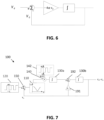
- FIG. 5 Exemplary embodiments of such systems 100 are shown in FIG. 5 , FIG. 7 , FIG. 17 , and FIG. 22 .
- the gate voltage or the source voltage may be toggled in order to get a toggling of the gate source voltage corresponding with said toggling signal.
- the drain voltage might be toggled simultaneously such that the drain source voltage remains stable.
- Toggling the source voltage may be advantageous for a common gate operation.
- the common gates of one or more transistor circuits may be kept at a fixed potential and the feedback voltage (i.e. the sum of the toggling signal and the integration signal or a processed version thereof) may be applied to the source. A version of said feedback voltage should then also be applied to the drain simultaneously such that a stable drain source voltage is obtained. Also this is of advantage for a common gate operation.
- instability in the drain source voltage may be compensated for by post processing in order to remove errors due to instability in the drain source voltage.
- a system 100 according to embodiments of the present invention may comprise different types of transistor systems.
- the inventors have found a particular transistor circuit, in accordance with embodiments of the present invention, which may be used for detecting and/or quantifying a chemical component such as for example bio-molecules or ions.
- the transistor circuit may be sensitive to chemical components of different kinds (e.g. different types of bio molecules or different kinds of ions).
- a field effect transistor may be used with a gate electrode that is sensitive to one or more chemical components.
- V DS V GS
- I DS f2 (V DS , V GS ). It was observed by the inventors that in most cases f2 is shifted compared to f1.
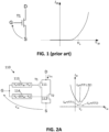
- FIG. 1 shows a classic n-channel field effect transistor with gate G, source S, and drain D terminals.
- I DS f(V b )
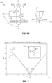
- the inventors have found that by combining the transistors in a transistor circuit the drain source current of this transistor circuit in function of the gate source voltage has a local minimum.
- the transistor circuit 110 comprises a first transistor 111 and a second transistor 112 with shared sources forming the source of the transistor circuit 110 and with shared drains forming the drain of the transistor circuit 110.
- a first voltage converter 113 converts a voltage at the gate of the transistor circuit 110, according to a transfer function with a first slope, into a voltage at the gate of the first transistor 111
- a second voltage converter 114 converts a voltage at the gate of the transistor circuit 110, according to a transfer function with a second slope, into a voltage at the gate of the second transistor 112.
- the first slope and the second slope have opposite signs.
- the first voltage converter 113 and the second voltage converter 114 may respectively be connected to the source of the first transistor 111 and the source of the second transistor 112 for creating the gate source voltage.
- the transistor circuit may comprise a third voltage converter 113' and a fourth voltage converter 114' respectively connected with the drain of the first transistor 111 and the drain of the second transistor 112 for driving the drains with a version of the signals on the source of the first and second transistor in order to achieve a constant drain source voltage of the first transistor and a constant drain source voltage of the second transistor, so that a stable drain source current can be obtained.
- this is of advantage for a constant gate operation under consideration of the two-transistor-circuit.
- a system in accordance with embodiments of the present invention may also work accepting some modulation of the drain source voltage. This would cause a shift in the detected minimum conduction point but in different applications this is acceptable. Users may for example be interested in the drift before and after exposure to a target chemical and the measured drift accepting drain source voltage modulation may be the same as the actual voltage drift of the specific voltage (e.g. Dirac voltage).
- the system may be configured for post processing of the found minimum to compensate for the changes in the drain source voltage.
- the transistor circuit 110 of FIG. 2 may be sensitive to any type of exposure.
- the two transistors may be transistors of the same kind. They may for example be two n-channel transistors (as it is shown in the schematic drawing), they may for example also be two p-channel transistors, two depletion transistors, or two zero threshold voltage transistors.
- the transistors may for example be characterized by a threshold voltage V th , that can be positive, negative, or even zero.
- Any transistors may be used. They could also be bipolar transistors or MOSFET transistors, which can also be used in their subthreshold ( ⁇ Vth) ranges.
- the voltage V GS1 applied between the gate and the source of the first transistor is increasing with the control voltage V GS according to a given slope (G).
- the voltage V GS2 applied between the gate and the source of the second transistor is decreasing with the control voltage V GS according to the opposite slope or gain factor (-G).
- the traces are mirrored in the vertical direction for the nonexposed transistors as they are in their initial state.
- I ds f(T1, T2).
- This local minimum will be shifted to other positions than V d if the voltage current characteristic of one of the transistors is shifted. This may for example occur when the first transistor or the second transistor is exposable to and sensitive for a chemical component. When exposing the sensitive transistor to the chemical component (e.g. a biomolecule, or an ion) this will result in a shift of the transfer function and therefore also in a shift of the local minimum. It is an advantage that the specific voltage of this minimum can be measured using a system in accordance with embodiments of the present invention.
- the chemical component e.g. a biomolecule, or an ion
- One of the transistors in FIG. 2 may be exposable to and sensitive for a chemical component while the other transistor is not exposed to the chemical component.
- the chemical component may be present in a given medium such as a liquid, a gel, or a gas.
- the transistors may for example also be graphene transistors wherein both transistors are exposed to the medium, but only one transistor is for example functionalized to be more sensitive for a given kind of chemical components (e.g. biomolecules) and the other one is not.
- chemical components e.g. biomolecules
- a single graphene field effect transistor can be used as transistor circuit 110 (see inset in FIG. 3 ).
- the reason therefore being that a single GFET has a local minimum in its current voltage characteristic.
- the specific gate source voltage at which the drain source current is at a local minimum is the Dirac voltage of the GFET.
- the GFET is integrated inside a closed loop-system acting as a low-pass filter which delivers an output voltage equal to the Dirac voltage of the GFET.
- the loop can be a sigma-delta modulator delivering a digital value of the Dirac voltage.
- the Dirac voltage is shifted during exposure of the GFET to a chemical component to which it is sensitive.
- both transistors might generate a transfer function which in case of a MOS transistor can for example be approximated by a 2 nd order in the neighborhood of the minimum conduction point:
- I DS I 1 + a 1 V GS ⁇ V d + b 1 V GS ⁇ V d 2 + I 2 ⁇ a 2 V GS ⁇ V d + b 2 V GS ⁇ V d 2
- I DS I 1 + I 2 + a 1 ⁇ a 2 V GS ⁇ V d + b 1 + b 2 V GS ⁇ V d 2
- the minimum conduction point is shifted if an electrical characteristic of one of the transistors is modified. This could be I 2 , a 2 , and/or b 2 if the transistor T 2 is exposed.
- the minimum conduction point is shifted if the gain a 2 or the threshold V th2 is modified, if the transistor T 2 would for instance be exposed to a chemical component.
- a transistor circuit as shown in FIG. 2 will have a local minimum (minimum conduction point) at a specific voltage. When one of the transistors is sensitive and exposed to the chemical component the specific voltage changes.
- the transistors of the transistor circuit may be chemical sensitive transistors (CHEMFETs), or ion sensitive transistors (ISFETS), but also graphene transistors (GFETs) in a differential approach. New application fields might be supported as well, for what graphene transistors are for instance not sensitive enough, e.g. measurements at very high temperature or harsh media.
- CHEMFETs chemical sensitive transistors
- ISFETS ion sensitive transistors
- GFETs graphene transistors
- the first transistor or the second transistor is exposable to and sensitive for a chemical component. In embodiments of the present invention only one of the transistors is exposable and this one is sensitive to the chemical component.
- the first transistor and the second transistor are exposable to a chemical component and only one is sensitive for the chemical component.
- only one may be functionalized and the other one not, while both are exposed.
- only one of the first transistor or the second transistor is exposable to a chemical component and the first transistor and the second transistor are sensitive for the chemical component.
- both transistors may be identical (e.g. two identical chemFETs) and only one is exposed to the chemical component.
- FIG. 3 shows the MIT model 10 of a GFET.
- the model was presented in "Mackin, C. (2016) Graphene chemical and biological sensors: Modeling, systems, and applications. PhD thesis at the Massachusetts Institute of Technology".
- FIG. 3 shows a fitting 11 by a simple linear and quadratic approximation.
- I DS V G I DS 0 + ⁇ V G ⁇ V d 2
- I DS V G I DS 1 ⁇ 2 ⁇ V 1 V G ⁇ V d ⁇ V 1 V G ⁇ V d ⁇ V 1
- I DS V G I DS 1 + 2 ⁇ V 1 V G ⁇ V d + V 1 V G ⁇ V d + V 1
- I DS V G I DS 1 + 2 ⁇ V 1 V G ⁇ V d ⁇ V 1 if V G ⁇ V d ⁇ V 1 ;
- an analog low-pass filter loop automatically adjusts the gate voltage to the Dirac point.
- the advantage of this approach is that a low-noise, high-resolution measurement of the Dirac point can be obtained in approximately the same time as the cited prior art systems would take for each single step of their gate voltage ramp.
- a simple analog circuit / digital circuit can be used what results in a low energy consumption.
- a system 100 for measuring a specific voltage (e.g. Dirac voltage) of transistor circuit 110 (e.g. a graphene field effect transistor or a transistor circuit as in FIG. 2 ) according to embodiments of the present invention comprises the transistor circuit 110, and a bias voltage generator 120 configured for generating a toggling signal, toggling between plus and minus a predefined bias voltage v G around a given bias point.
- the bias point is thus the average level of the toggling signal generated by the bias voltage generator.
- the given bias point may for example be zero volt.
- the invention is, however, not limited thereto.
- the given bias point may also be different from zero.
- the system 100 moreover, comprises a multiplier 140 configured for generating an electrical signal by multiplying an electrical signal which is a function of the drain source current of the transistor circuit (e.g. a channel current I DS of e.g. a graphene field effect transistor 110, or the sum of the currents I DS through the transistors T1 and T2 in the circuit of FIG. 2 ), with a waveform alternating between two predefined values +A and -A which alternates synchronously with the toggling signal.
- the alternating waveform applied to the multiplier could thereby be delayed (phase shifted) with respect to the gate voltage toggling signal.
- the predefined value A may for example be equal to 1.
- the factor A is a multiplication factor for the signal to be integrated.
- This signal can be the drain current of the transistor circuit (e.g. the GFET drain current), a multiplication of the drain current, the output of a trans-impedance amplifier and is referred to as the transistor circuit signal.
- This signal is integrated by an integrator which also has a gain factor.
- A is selected such that the product of all multiplication factors applied to the transistor circuit signal do not lead to saturation of the first integrator at any time. This total gain factor impacts the loop bandwidth and stability.
- the feedback or feedforward factors are preferably chosen to achieve the desired bandwidth and stability taking into account the transistor circuit characteristic and all multiplicative factors involved in the integration of the transistor circuit signal.
- A may for example be in a range between 0.001 and 1000.
- the system 100 moreover, comprises one or more integrators 130 wherein a first integrator 130, of the one or more integrators 130, is configured for integrating the electrical signal from the multiplier 140, and wherein if more integrators 130 are present, linear combinations of output signals of the integrators are provided to the further integrators 130.
- the system 100 moreover, comprises a summator 150 configured for summing the toggling signal of the bias voltage generator 120 and an integration signal, or a processed version thereof, wherein the integration signal is obtained by linearly combining outputs of the one or more integrators 130.
- the system comprises a sample and hold circuit for sampling and holding the integration signal for obtaining the processed version of the integration signal.
- the integration signal may be sampled before the toggling from -A to +A (or from +A to -A) of the toggling signal applied to the multiplier and held for one full period of the toggling signal applied to the multiplier (same frequency as the toggling voltage applied to the gate but possible delay) so until the next toggling from -A to +A (or from +A to -A).
- the invention is, however, not limited thereto.
- a sample and hold circuit is not strictly required and if a sample and hold circuit is present, the sample moment may be selected different as specified above.
- the last integrator in the loop may be implemented with a switched-capacitor circuit for providing the sample and hold functionality.
- a loop is formed.
- the low-pass filter loop has to integrate a quantity that is 0 when the gate voltage is at the specific voltage and which has a linear dependency on the gate voltage in the neighborhood of the specific voltage.
- the current vs. gate voltage characteristic is a 2 nd -order curve so its derivative is a linear function of the gate voltage which is null at the local minimum of the current.
- FIG. 4 This integration of the drain source current of the transistor circuit is illustrated in FIG. 4 .
- a basic first order measurement loop of a system for measuring the specific voltage at the local minimum e.g. the Dirac voltage in case the transistor circuit is a GFET
- FIG. 5 shows the transistor circuit 110 (represented by its characteristic graph with local minimum in the current voltage characteristic), the bias voltage generator 120, the first integrator 130, the multiplier 140, and the summator 150.
- the bias point of the bias voltage generator is 0 and as a result thereof the integration signal will in this example be the specific voltage corresponding with the local minimum. If the bias point is different from zero, the integration signal will be the specific voltage minus the bias point.
- the integrator integrates the difference between 2 transistor circuit currents corresponding to 2 different gate voltages in order to integrate the slope of the current vs. gate voltage characteristic rather than the current itself.
- the basic loop illustrated in FIG. 5 forms a 1 st order linear system of which the block diagram is shown in FIG. 6 .
- the system comprises exactly two integrators wherein an input signal of the second integrator is the sum of an output signal of the first integrator and an output signal of the second integrator multiplied with a predefined constant a 1 .
- An example thereof is illustrated in FIG. 7 . It shows the transistor circuit 110 (this may for example be a GFET or a transistor circuit as illustrated in FIG.
- the bias voltage generator 120 the bias voltage generator 120, the first integrator 130a, the second integrator 130b, the multiplier 140, the summator 150, a multiplier 191 for multiplying an output signal of the second integrator 130b with a predefined constant a 1 , and a summator 192 for summing the output signal of the first integrator 130a and the output signal of the second integrator 130b.
- K1 holds the product multiplication factors like a possible trans-impedance factor, the amplitude of the multiplication waveform (A) and the capacitor used in the implementation of the of the continuous time integrator.
- K2 holds the time-constant of the second continuous time integrator.
- the system has a predefined bias voltage modulation which is small enough such that the modulation is inside the quadratic region of the transistor circuit characteristic (e.g. GFET characteristic).
- the transistor circuit characteristic e.g. GFET characteristic
- the linear system description is valid when the predefined bias voltage v G > 2 V 1 and the gate voltages involved in the difference I DS ( V G + v G ) - I DS ( V G - v G ) are located in both linear regions of the transistor circuit characteristic: V G - v G ⁇ V d - V 1 and V G + v G ⁇ V d + V 1 .
- Using a large gate voltage modulation allows to search for the specific voltage over a large gate voltage range.
- the loop can be implemented with continuous time integrator or discrete-time integrators.
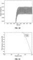
- the following Matlab simulation results show the behavior of the described 2 nd -order system for which the transistor circuit is a GFET.
- a first loop was constructed with 70 Hz bandwidth approximately.
- the predefined bias voltage was +/- 0.2V (i.e. large gate voltage modulation) at 1 kHz.
- the loop parameters were calculated considering the gain value 4 ⁇ V 1 .
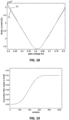
- the simulation results in FIG. 9 and FIG. 10 show that the output of the filter reaches the Dirac voltage in less than 50 ms (see FIG. 7 ).
- FIG. 11 shows the frequency response of the second order system.
- the following simulation results show a second loop design with the same bandwidth of 70 Hz but using a predefined bias voltage v G of 0.01V (i.e. small gate voltage modulation) instead of 0.2V.
- the loop parameters were calculated considering the gain value 4 ⁇ v G .
- the integrator time constants are therefore different from the ones used with the larger bias voltage.
- the plot in FIG. 12 shows the settling at the output of the second order system with a small gate voltage modulation. The correct value is reached within 100 ms starting from discharged integrators.
- the loop only starts working when V G enters the quadratic region. This is further explained in the paragraph below.
- FIG. 13 shows a zoomed-in version of FIG. 12 between 0.598 and 0.618 V.
- FIGs. 14, 15 and 16 show the results for a loop with less than 7 Hz bandwidth and large gate signal modulation.
- the filter settles within 500 ms with 15 ⁇ V residual oscillation.
- FIG. 14 shows the frequency response of the 2 nd -order system with 7Hz bandwidth and large gate voltage modulation.
- FIG. 15 shows a Matlab simulation result illustrating the settling of the 7Hz-bandwidth, 2 nd -order system with large gate voltage modulation.
- FIG. 15 shows a Matlab simulation result illustrating the residual oscillation at the output of the 7Hz-bandwidth, 2 nd -order system with large gate voltage modulation.
- the residual oscillation can be reduced by introducing the sample and hold circuit. It is, however, not strictly required.
- the system 100 comprises a quantizer 160 which is configured for quantizing the integrator signal at a predefined sampling frequency.
- the system 100 moreover, comprises a digital to analog converter 170 for converting the quantized signal into an analog signal for summing with the toggling signal at the summator 150.
- the low-pass filter loop is converted into sigma-delta modulator. This is possible because of the linear relationship between the current difference, ⁇ I DS , and the gate voltage.
- FIG. 17 shows a schematic diagram of an exemplary system for measuring the specific voltage corresponding with the local minimum of the current of a transistor circuit (this may for example be a GFET), comprising a 2 nd -order sigma-delta ADC, in accordance with embodiments of the present invention.
- the system 100 of FIG. 17 comprises the transistor circuit 110, a bias voltage generator 120, a digital to analog converter 170, a summator 150 for summing the signal from the bias voltage generator 120 and the signal from the digital to analog converter 170.
- the output of the summator 150 is connected to the gate of the transistor circuit 110.
- the system 100 furthermore comprises a waveform generator 142 configured for generating a waveform alternating between +A and -A, and a multiplier 140 configured for multiplying the waveform of the waveform generator with an electrical signal which is a function of a channel current of e.g. the GFET or the resulting sum of the two channel currents of the both transistors of the transistor circuit 110.
- the system furthermore, comprises a first integrator 130a for integrating the signal from the multiplier 140 and a second integrator 130b for integrating the sum, obtained using a summator 192, of the signal from the first integrator 130a and the quantized output of the second integrator multiplied with a predefined factor a1 using a multiplier 191.
- the system furthermore, comprises a 1-bit quantizer for quantizing the output signal of the second integrator 130b.
- the system furthermore, comprises a decimation filter 180 at the output of the quantizer.
- the sigma-delta loop toggles the gate voltage V G between 2 fixed voltages, V ref 1 and V ref 2 , within the region of validity of the linear relationship between the current difference and the gate voltage.
- the output of the 1-bit quantizer is, therefore, connected to a switch of the digital to analog converter 170 which switches between V ref 1 and V ref 2 and connects them alternatingly to the summator 150.
- the gate voltages In order for a linear relationship to be valid, the gate voltages must be chosen as follows. If one uses a small gate voltage modulation (i.e. within the quadratic region of the transistor circuit), v G , all 4 gate voltages have to be in the central quadratic part of the transistor circuit characteristic. In embodiments of the present invention small v G signal modulation is used in the quadratic region so that at the first predefined voltage, the gate voltage is toggling between 2 levels both at the left side of the specific voltage (the gate voltage is smaller than the specific voltage V d ) and at the second predefined voltage, both levels will be at the right side of the specific voltage (the gate voltage is larger than the specific voltage V d ).
- the sigma-delta loop delivers a bit stream alternating between 0 and 1.
- D be the ratio between the number of 1s and the total number of bits in the bit stream.
- the sigma delta loop will adjust D such that the average of ⁇ I DS is 0. ⁇ I DS thereby is proportional to the slope of the transistor circuit I DS vs. V GS characteristic and becomes 0 at the specific voltage.
- the sigma-delta modulator generates its feedback signal such that the quantity that is integrated by the integrator is 0 in average.
- I DS _ D ⁇ I DS 2 + 1 ⁇ D ⁇ I DS 1
- I DS _ D 4 ⁇ V 1 V ref 2 ⁇ V d + 1 ⁇ D 4 ⁇ V 1 V ref 1 ⁇ V d
- the invention is not limited to sigma-delta modulators of the second order. Also sigma delta modulators of different orders may be used.
- the integrators can be continuous-time or discrete-time integrators.
- a Matlab simulation of an exemplary system, in accordance with embodiments of the present invention and illustrated in FIG. 17 , applied to the GFET described by the MIT model has been executed.
- the system is able to measure a Dirac voltage for a GFET or the voltage for a minimum I DS of the both Ts in a transistor circuit 110 (i.e. the specific voltage of the transistor circuit) in the range from V ref 1 to V ref 2 .
- the predefined bias voltage also referred to as the modulation voltage
- v G must meet the following condition: v G ⁇ V ref 2 ⁇ V ref 1 + V 1
- the system comprises a decimation filter.
- the decimation filter may for example be a sinc3 filter with an over-sampling rate of 256.
- V ref 1 + v G 0.695 V
- V ref 1 ⁇ v G 0.405 V
- V ref 2 + v G 0.795 V
- V ref 2 ⁇ v G 0.505 V
- FIG. 19 shows the output of the decimation filter converted to voltage.
- the output of the filter settles within 3*256 samples corresponding to a settling time of 768 ms.
- FIG. 20 shows a plot zoomed to the settled output of the decimation filter.
- the reference voltages may be selected closer to the actual Dirac voltage.
- the GFET is operated at 4 gates voltages where the linear approximation holds better which yields a better estimation of the Dirac point. This is illustrated in FIG. 21 which shows a plot zoomed to the settled output of the decimation filter for the values cited above.
- the quantizer 160 is a multi-bit quantizer with a predefined number of N q bits, wherein the digital to analog converter 170 has N q bits.
- An exemplary embodiment of such a system is shown in FIG. 22 .
- the schematic diagram is similar to the schematic in FIG. 17 except for the fact that the quantizer is a N q bits quantizer and the digital to analog converter 170 has N q bits.
- the multi-bit approach allows to search for the specific voltage in a wide range.
- the initial settling of the loop will take care of the initial guess of the specific voltage and eventually, the DAC will toggle between 2 or 3 levels only.
- the multi-bit quantizer inside the sigma-delta loop is a low-resolution ADC. In embodiments of the present invention it is not just converting the output of the current integrator but a linear combination of the outputs of several integrators. In the example the output voltage of the second integrator is converted.
- the output of the low-resolution multi-bit quantizer is directly connected to the low-resolution DAC without any processing by a control circuit configured to determine a voltage value applied to a control electrode of the control circuit.
- the reference voltages can be extended beyond the regions of validity of the linear relationship if a multi-bit quantizer is used in the sigma-delta loop.
- the loop will feedback 2 N q different possible DAC voltages which are uniformly spread over the range [ V ref 1 ; V ref 2 ], N q being the number of bits of the quantizer used inside the loop. After some settling time, the loop will automatically converge to a situation where the feedback gate voltage will toggle between a few of those possible feedback voltages only, all being located in the neighborhood of the specific voltage.
- the number of bits of the quantizer is chosen such that the several consecutive DAC voltages are inside the region of validity of the linear relationship between the current difference and the gate voltage.
- the transistor circuit is a GFET.
- the GFET model is the same as before.
- the current difference is linear vs. the gate voltage in the gate voltage range [ V d - 0.045 ; V d + 0.045].
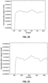
- FIG. 23 shows a plot of the decimation filter output in function of the sample number.
- FIG. 24 shows a zoom to the output of the decimation filter.
- FIG. 25 shows the 5-bit quantizer output in function of the sample number.
- a small vG modulation signal preferably there are several consecutive DAC voltages inside the quadratic region of the GFET IDS vs. V G characteristic so that the slope (the quantity that is integrated) is proportional to the applied gate voltage. That is the condition to form a linear feedback system and have an accurate measurement of the Dirac voltage as the successive DAC voltages. Indeed several DAC voltage outputs Vdac+/-vG are preferably in the quadratic region.
- the system 100 may comprise an upper system (e.g. a controller) for selecting the reference voltages of the system 100 so that the loop always starts in a first stage wherein the predefined bias voltage v G is selected such that the sum obtained by the summator is in a linear region of the graphene field effect transistor characteristic and settles down to a first Dirac voltage that is preferably in the quadratic region.
- the upper system is configured for selecting the predefined bias voltage such that the sum obtained by the summator is inside the quadratic region of the graphene field effect transistor characteristic.
- the system then settles down to a second Dirac voltage which may be more or at least as accurate as the first obtained Dirac voltage.
- a system is obtained which performs the Dirac point measurement in a two stage approach.
Landscapes
- Engineering & Computer Science (AREA)
- General Physics & Mathematics (AREA)
- Physics & Mathematics (AREA)
- Microelectronics & Electronic Packaging (AREA)
- General Engineering & Computer Science (AREA)
- Environmental & Geological Engineering (AREA)
- Computer Hardware Design (AREA)
- Health & Medical Sciences (AREA)
- Toxicology (AREA)
- Theoretical Computer Science (AREA)
- Measurement Of Current Or Voltage (AREA)
- Amplifiers (AREA)
- Compression, Expansion, Code Conversion, And Decoders (AREA)
- Investigating Or Analyzing Materials By The Use Of Electric Means (AREA)
Claims (15)
- Ein System (100) zum Charakterisieren einer Transistorschaltung (110), die ein Gate, eine Source und einen Drain umfasst, wobei die Transistorschaltung so konfiguriert ist, dass eine Drain-Source-Strom-zu-Gate-Source-Spannungsübertragungsfunktion ein lokales Minimum für eine spezifische Spannung aufweist, wobei das System zum Messen der spezifischen Spannung konfiguriert ist, wobei das System Folgendes umfasst:- die Transistorschaltung (110),- einen Vorspannungsgenerator (120), der zum Erzeugen eines Umschaltsignals konfiguriert ist, das zwischen plus und minus einer vordefinierten Vorspannung VG um einen gegebenen Vorspannungspunkt umschaltet,- einen oder mehrere Integratoren (130),- einen Multiplizierer (140), der zum Erzeugen eines elektrischen Signals konfiguriert ist, indem er ein elektrisches Signal, das eine Funktion des Drain-Source-Stroms der Transistorschaltung (110) ist, mit einer Wellenform multipliziert, die zwischen zwei vordefinierten Werten plus und minus A wechselt, die synchron mit dem Umschalten wechseln,- wobei ein erster Integrator (130) des einen oder der mehreren Integratoren (130) zum Integrieren des elektrischen Signals vom Multiplizierer (140) konfiguriert ist, und wobei, wenn mehrere Integratoren (130) vorhanden sind, Linearkombinationen von Ausgangssignalen der Integratoren den weiteren Integratoren (130) zur Verfügung gestellt werden,- einen Summierer (150), der zum Summieren des Umschaltsignals und eines Integrationssignals oder einer verarbeiteten Version davon konfiguriert ist, wobei das Integrationssignal durch lineares Kombinieren von Ausgängen des einen oder der mehreren Integratoren (130) erhalten wird und zum Ausgeben der Summe als Gate-Source-Spannung der Transistorschaltung konfiguriert ist.
- Ein System (100) nach Anspruch 1, wobei die Transistorschaltung (110) Folgendes umfasst:- einen ersten Transistor (111) und einen zweiten Transistor (112),- einen ersten Spannungswandler (113), der zum Umwandeln einer Spannung am Gate der Transistorschaltung (110) oder an der Source der Transistorschaltung (110) gemäß einer Übertragungsfunktion mit einer ersten Steigung in eine Gate-Source-Spannung zwischen dem Gate und der Source des ersten Transistors (111) konfiguriert ist,- einen zweiten Spannungswandler (114), der zum Umwandeln einer Spannung am Gate der Transistorschaltung (110) oder an der Source der Transistorschaltung (110) gemäß einer Übertragungsfunktion mit einer zweiten Steigung in eine Gate-Source-Spannung zwischen dem Gate und der Source des zweiten Transistors (112) konfiguriert ist,- wobei die erste Steigung und die zweite Steigung entgegengesetzte Vorzeichen haben.
- Ein System (100) nach Anspruch 2, wobei der erste Transistor (111) oder der zweite Transistor (112) einer chemischen Komponente ausgesetzt werden kann und für diese empfindlich ist, oder wobei der erste Transistor (111) und der zweite Transistor (112) einer chemischen Komponente ausgesetzt werden können und nur einer für die chemische Komponente empfindlich ist, oder wobei entweder der erste Transistor (111) oder der zweite Transistor (112) einer chemischen Komponente ausgesetzt werden kann und wobei der erste Transistor (111) und der zweite Transistor (112) für die chemische Komponente empfindlich sind.
- Ein System (100) nach einem der Ansprüche 2 oder 3, wobei der erste Transistor (111) und der zweite Transistor (112) Metall-Oxid-Halbleiter-FET oder bipolare Transistoren sind.
- Ein System (100) nach Anspruch 1, wobei die Transistorschaltung (110) ein Graphen-FET ist.
- Ein System (100) nach einem der vorstehenden Ansprüche, wobei das System eine Abtast- und Halteschaltung zum Abtasten und Halten des Integrationssignals umfasst, um die verarbeitete Version des Integrationssignals zu erhalten.
- Ein System (100) nach einem der Ansprüche 1 bis 5, wobei das System genau einen Integrator (130) umfasst.
- Ein System (100) nach einem der Ansprüche 1 bis 5, wobei das System genau zwei Integratoren (130a, 130b) umfasst, wobei ein Eingangssignal des zweiten Integrators (130b) die Summe eines Ausgangssignals des ersten Integrators (130a) und eines Ausgangssignals des zweiten Integrators multipliziert mit einer vordefinierten Konstante a1 ist.
- Ein System (100) nach einem der vorstehenden Ansprüche, wobei die vordefinierte Vorspannung derart ist, dass die durch den Summierer erhaltene Summe innerhalb eines quadratischen Bereichs der Transistorschaltungskennlinie liegt.
- Ein System (100) nach einem der Ansprüche 1 bis 8, wobei die vordefinierte Vorspannung derart ist, dass die durch den Summierer erhaltene Summe in einem linearen Bereich der Transistorschaltungskennlinie liegt.
- Ein System (100) nach einem der vorstehenden Ansprüche, wobei in einer ersten Stufe die vordefinierte Vorspannung derart ist, dass die durch den Summierer erhaltene Summe in einem linearen Bereich der Transistorschaltungskennlinie liegt, und wobei in einer zweiten Stufe die vordefinierte Vorspannung derart ist, dass die durch den Summierer erhaltene Summe innerhalb eines quadratischen Bereichs der Transistorschaltungskennlinie liegt.
- Ein System (100) nach einem der vorstehenden Ansprüche, wobei das System (100) einen Quantisierer (160) umfasst, der zum Quantisieren des Integratorsignals mit einer vordefinierten Abtastfrequenz konfiguriert ist, und einen Digital-Analog-Wandler (170) zum Umwandeln des quantisierten Signals in ein analoges Signal zum Summieren mit dem Umschaltsignal am Summierer (150).
- Ein System (100) nach Anspruch 12, wobei der Digital-Analog-Wandler (170) zwischen einer ersten vordefinierten Referenzspannung für einen digitalen Null-Eingang und einer zweiten vordefinierten Referenzspannung für einen digitalen Eins-Eingang umschaltet, wobei die erste und zweite Referenzspannung und die vordefinierte Vorspannung so gewählt sind, dass das Umschalten mit der vordefinierten Vorspannung zu einer Spannung im linken linearen Bereich und einer Spannung im rechten linearen Bereich der Transistorschaltung führt.
- Ein System (100) nach Anspruch 12, wobei der Digital-Analog-Wandler (170) zwischen einer ersten vordefinierten Referenzspannung für einen digitalen Null-Eingang und einer zweiten vordefinierten Referenzspannung für einen digitalen Eins-Eingang umschaltet, wobei die erste Referenzspannung und die vordefinierte Vorspannung so gewählt sind, dass das Umschalten mit der vordefinierten Vorspannung zu einer Spannung im linken Teil eines quadratischen Bereichs und einer Spannung im selben linken Teil des quadratischen Bereichs führt und wobei die zweite Referenzspannung und die vordefinierte Vorspannung so gewählt sind, dass ein Umschalten mit der vordefinierten Vorspannung zu einer Spannung im rechten Teil des quadratischen Bereichs und einer Spannung im selben rechten Teil des quadratischen Bereichs der Transistorschaltung führt.
- Ein System (100) nach Anspruch 12, wobei der Quantisierer (160) ein Multibit-Quantisierer mit einer vordefinierten Anzahl von Nq Bits ist, wobei der Digital-Analog-Wandler (170) Nq Bits aufweist.
Applications Claiming Priority (2)
| Application Number | Priority Date | Filing Date | Title |
|---|---|---|---|
| EP22206710.0A EP4369005A1 (de) | 2022-11-10 | 2022-11-10 | Dirac-spannungsmessung eines graphen-fet |
| EP23168026.5A EP4369006A1 (de) | 2022-11-10 | 2023-04-14 | System zur charakterisierung einer transistorschaltung |
Publications (3)
| Publication Number | Publication Date |
|---|---|
| EP4369007A1 EP4369007A1 (de) | 2024-05-15 |
| EP4369007B1 true EP4369007B1 (de) | 2024-11-20 |
| EP4369007C0 EP4369007C0 (de) | 2024-11-20 |
Family
ID=88188830
Family Applications (1)
| Application Number | Title | Priority Date | Filing Date |
|---|---|---|---|
| EP23201304.5A Active EP4369007B1 (de) | 2022-11-10 | 2023-10-02 | System zur charakterisierung einer transistorschaltung |
Country Status (4)
| Country | Link |
|---|---|
| US (1) | US12282054B2 (de) |
| EP (1) | EP4369007B1 (de) |
| JP (1) | JP7757370B2 (de) |
| CN (1) | CN118016720B (de) |
Families Citing this family (1)
| Publication number | Priority date | Publication date | Assignee | Title |
|---|---|---|---|---|
| JP2024165266A (ja) * | 2023-05-17 | 2024-11-28 | 富士電機株式会社 | 試験方法 |
Family Cites Families (10)
| Publication number | Priority date | Publication date | Assignee | Title |
|---|---|---|---|---|
| US5039941A (en) * | 1990-07-27 | 1991-08-13 | Intel Corporation | Voltage threshold measuring circuit |
| US5194802A (en) * | 1991-10-25 | 1993-03-16 | General Electric Company | Transconductance current regulator using precisely sampled charges for current control |
| EP1978635B1 (de) * | 2007-04-04 | 2013-01-23 | TELEFONAKTIEBOLAGET LM ERICSSON (publ) | Schaltung und Verfahren zur Reduzierung von Nichtlinearitäten zweiter und dritter Ordnung |
| US8054360B2 (en) * | 2009-02-02 | 2011-11-08 | Advasense Technologies Ltd. | Device and method for providing a reference signal |
| KR101878738B1 (ko) * | 2011-09-16 | 2018-07-17 | 삼성전자주식회사 | 반도체 장치 및 반도체 장치의 동작 방법 |
| WO2018012076A1 (ja) | 2016-07-12 | 2018-01-18 | 三菱電機株式会社 | 電磁波検出器及び電磁波検出器アレイ |
| US10289137B2 (en) * | 2016-10-06 | 2019-05-14 | Infineon Technologies Austria Ag | System and method for a current controller |
| EP3657165B1 (de) | 2018-11-23 | 2026-04-15 | Infineon Technologies AG | Verfahren zur bereitstellung von kalibrierdaten für eine gassensorvorrichtung, verfahren zur kalibrierung einer gassensorvorrichtung, systeme und computerprogrammprodukte |
| CN113008967A (zh) | 2020-06-29 | 2021-06-22 | 山东大学 | 一种无标记石墨烯场效应晶体管柔性生物传感器及其制备方法和应用 |
| CN115032515A (zh) * | 2022-06-30 | 2022-09-09 | 北京华峰测控技术股份有限公司 | 场效应管动态阈值电压测量方法及测试设备 |
-
2023
- 2023-10-02 EP EP23201304.5A patent/EP4369007B1/de active Active
- 2023-10-25 JP JP2023183089A patent/JP7757370B2/ja active Active
- 2023-11-02 US US18/500,249 patent/US12282054B2/en active Active
- 2023-11-10 CN CN202311503296.4A patent/CN118016720B/zh active Active
Also Published As
| Publication number | Publication date |
|---|---|
| CN118016720B (zh) | 2026-02-03 |
| CN118016720A (zh) | 2024-05-10 |
| KR20240068579A (ko) | 2024-05-17 |
| JP2024070232A (ja) | 2024-05-22 |
| JP7757370B2 (ja) | 2025-10-21 |
| US20240159820A1 (en) | 2024-05-16 |
| EP4369007C0 (de) | 2024-11-20 |
| US12282054B2 (en) | 2025-04-22 |
| EP4369007A1 (de) | 2024-05-15 |
Similar Documents
| Publication | Publication Date | Title |
|---|---|---|
| US11652458B2 (en) | Amplification interface, and corresponding measurement system and method for calibrating an amplification interface | |
| Bartic et al. | Monitoring pH with organic-based field-effect transistors | |
| US6869216B1 (en) | Digitizing temperature measurement system | |
| US20220221420A1 (en) | Methods and systems for readout of nanogap sensors | |
| EP4369007B1 (de) | System zur charakterisierung einer transistorschaltung | |
| US10713446B2 (en) | Multiplier circuit, corresponding device and method | |
| CN112513598B (zh) | 用于温度感测的方法和电路、温度传感器以及电器 | |
| US10756745B2 (en) | Electrical circuit for biasing or measuring current from a sensor | |
| US11817838B2 (en) | Amplification interface, and corresponding measurement system and method for operating an amplification interface | |
| JP2011147117A (ja) | Ad変換装置および制御方法 | |
| US20060055580A1 (en) | Controlled power source, in particular for a digital analogue converter in continuous time sigma delta modulators | |
| EP4369006A1 (de) | System zur charakterisierung einer transistorschaltung | |
| KR101875464B1 (ko) | 전력 소모량 및 동적범위가 개선된 전류 판독 회로 | |
| Thanachayanont | A 1-V, 330-nW, 6-Bit Current-Mode Logarithmic Cyclic ADC for ISFET-Based p H Digital Readout System | |
| KR102954543B1 (ko) | 트랜지스터 회로 특성화 시스템 | |
| JP5237685B2 (ja) | センサ装置 | |
| US11402275B2 (en) | Sensor apparatus | |
| Zhang et al. | A High Resolution Chemical Sensing Front-end with Integrated Sigma Delta Quantisation | |
| US10483993B1 (en) | Residue amplifier | |
| Cortes-Guzman et al. | Linear pulse-frequency modulator isfet with a wide supply range | |
| EP4465538A1 (de) | Delta-sigma-messvorrichtung | |
| RU2791439C1 (ru) | Способ выравнивания параметров каналов регистрации многоканального нанопроводного детектора | |
| US20230179221A1 (en) | A Current-to-Digital Converter | |
| SU1203701A1 (ru) | Преобразователь тока в частоту | |
| Pandey et al. | Switched capacitor circuit realization of sigma-delta adc for temperature sensor |
Legal Events
| Date | Code | Title | Description |
|---|---|---|---|
| PUAI | Public reference made under article 153(3) epc to a published international application that has entered the european phase |
Free format text: ORIGINAL CODE: 0009012 |
|
| STAA | Information on the status of an ep patent application or granted ep patent |
Free format text: STATUS: REQUEST FOR EXAMINATION WAS MADE |
|
| 17P | Request for examination filed |
Effective date: 20240326 |
|
| AK | Designated contracting states |
Kind code of ref document: A1 Designated state(s): AL AT BE BG CH CY CZ DE DK EE ES FI FR GB GR HR HU IE IS IT LI LT LU LV MC ME MK MT NL NO PL PT RO RS SE SI SK SM TR |
|
| GRAP | Despatch of communication of intention to grant a patent |
Free format text: ORIGINAL CODE: EPIDOSNIGR1 |
|
| STAA | Information on the status of an ep patent application or granted ep patent |
Free format text: STATUS: GRANT OF PATENT IS INTENDED |
|
| INTG | Intention to grant announced |
Effective date: 20240716 |
|
| GRAS | Grant fee paid |
Free format text: ORIGINAL CODE: EPIDOSNIGR3 |
|
| GRAA | (expected) grant |
Free format text: ORIGINAL CODE: 0009210 |
|
| STAA | Information on the status of an ep patent application or granted ep patent |
Free format text: STATUS: THE PATENT HAS BEEN GRANTED |
|
| AK | Designated contracting states |
Kind code of ref document: B1 Designated state(s): AL AT BE BG CH CY CZ DE DK EE ES FI FR GB GR HR HU IE IS IT LI LT LU LV MC ME MK MT NL NO PL PT RO RS SE SI SK SM TR |
|
| REG | Reference to a national code |
Ref country code: GB Ref legal event code: FG4D |
|
| REG | Reference to a national code |
Ref country code: CH Ref legal event code: EP |
|
| REG | Reference to a national code |
Ref country code: DE Ref legal event code: R096 Ref document number: 602023001104 Country of ref document: DE |
|
| REG | Reference to a national code |
Ref country code: IE Ref legal event code: FG4D |
|
| U01 | Request for unitary effect filed |
Effective date: 20241120 |
|
| U07 | Unitary effect registered |
Designated state(s): AT BE BG DE DK EE FI FR IT LT LU LV MT NL PT RO SE SI Effective date: 20241126 |
|
| RAP4 | Party data changed (patent owner data changed or rights of a patent transferred) |
Owner name: MELEXIS TECHNOLOGIES NV |
|
| U1H | Name or address of the proprietor changed after the registration of the unitary effect |
Owner name: MELEXIS TECHNOLOGIES NV; BE |
|
| PG25 | Lapsed in a contracting state [announced via postgrant information from national office to epo] |
Ref country code: IS Free format text: LAPSE BECAUSE OF FAILURE TO SUBMIT A TRANSLATION OF THE DESCRIPTION OR TO PAY THE FEE WITHIN THE PRESCRIBED TIME-LIMIT Effective date: 20250320 Ref country code: HR Free format text: LAPSE BECAUSE OF FAILURE TO SUBMIT A TRANSLATION OF THE DESCRIPTION OR TO PAY THE FEE WITHIN THE PRESCRIBED TIME-LIMIT Effective date: 20241120 |
|
| PG25 | Lapsed in a contracting state [announced via postgrant information from national office to epo] |
Ref country code: ES Free format text: LAPSE BECAUSE OF FAILURE TO SUBMIT A TRANSLATION OF THE DESCRIPTION OR TO PAY THE FEE WITHIN THE PRESCRIBED TIME-LIMIT Effective date: 20241120 |
|
| PG25 | Lapsed in a contracting state [announced via postgrant information from national office to epo] |
Ref country code: NO Free format text: LAPSE BECAUSE OF FAILURE TO SUBMIT A TRANSLATION OF THE DESCRIPTION OR TO PAY THE FEE WITHIN THE PRESCRIBED TIME-LIMIT Effective date: 20250220 |
|
| PG25 | Lapsed in a contracting state [announced via postgrant information from national office to epo] |
Ref country code: GR Free format text: LAPSE BECAUSE OF FAILURE TO SUBMIT A TRANSLATION OF THE DESCRIPTION OR TO PAY THE FEE WITHIN THE PRESCRIBED TIME-LIMIT Effective date: 20250221 |
|
| PG25 | Lapsed in a contracting state [announced via postgrant information from national office to epo] |
Ref country code: PL Free format text: LAPSE BECAUSE OF FAILURE TO SUBMIT A TRANSLATION OF THE DESCRIPTION OR TO PAY THE FEE WITHIN THE PRESCRIBED TIME-LIMIT Effective date: 20241120 |
|
| PG25 | Lapsed in a contracting state [announced via postgrant information from national office to epo] |
Ref country code: RS Free format text: LAPSE BECAUSE OF FAILURE TO SUBMIT A TRANSLATION OF THE DESCRIPTION OR TO PAY THE FEE WITHIN THE PRESCRIBED TIME-LIMIT Effective date: 20250220 |
|
| PG25 | Lapsed in a contracting state [announced via postgrant information from national office to epo] |
Ref country code: SM Free format text: LAPSE BECAUSE OF FAILURE TO SUBMIT A TRANSLATION OF THE DESCRIPTION OR TO PAY THE FEE WITHIN THE PRESCRIBED TIME-LIMIT Effective date: 20241120 |
|
| PG25 | Lapsed in a contracting state [announced via postgrant information from national office to epo] |
Ref country code: SK Free format text: LAPSE BECAUSE OF FAILURE TO SUBMIT A TRANSLATION OF THE DESCRIPTION OR TO PAY THE FEE WITHIN THE PRESCRIBED TIME-LIMIT Effective date: 20241120 |
|
| PG25 | Lapsed in a contracting state [announced via postgrant information from national office to epo] |
Ref country code: CZ Free format text: LAPSE BECAUSE OF FAILURE TO SUBMIT A TRANSLATION OF THE DESCRIPTION OR TO PAY THE FEE WITHIN THE PRESCRIBED TIME-LIMIT Effective date: 20241120 |
|
| PLBE | No opposition filed within time limit |
Free format text: ORIGINAL CODE: 0009261 |
|
| STAA | Information on the status of an ep patent application or granted ep patent |
Free format text: STATUS: NO OPPOSITION FILED WITHIN TIME LIMIT |
|
| 26N | No opposition filed |
Effective date: 20250821 |
|
| U20 | Renewal fee for the european patent with unitary effect paid |
Year of fee payment: 3 Effective date: 20250923 |