EP4366174A1 - Verfahren zur steuerung der stromversorgung zur hf-signalverstärkung und kommunikationsvorrichtung zur durchführung davon - Google Patents
Verfahren zur steuerung der stromversorgung zur hf-signalverstärkung und kommunikationsvorrichtung zur durchführung davon Download PDFInfo
- Publication number
- EP4366174A1 EP4366174A1 EP22895896.3A EP22895896A EP4366174A1 EP 4366174 A1 EP4366174 A1 EP 4366174A1 EP 22895896 A EP22895896 A EP 22895896A EP 4366174 A1 EP4366174 A1 EP 4366174A1
- Authority
- EP
- European Patent Office
- Prior art keywords
- mode
- downlink
- condition
- error rate
- block error
- Prior art date
- Legal status (The legal status is an assumption and is not a legal conclusion. Google has not performed a legal analysis and makes no representation as to the accuracy of the status listed.)
- Pending
Links
- 238000000034 method Methods 0.000 title claims abstract description 141
- 238000004891 communication Methods 0.000 title claims abstract description 112
- 230000003321 amplification Effects 0.000 title 1
- 238000003199 nucleic acid amplification method Methods 0.000 title 1
- 230000005540 biological transmission Effects 0.000 claims abstract description 34
- 230000006870 function Effects 0.000 description 10
- 238000010586 diagram Methods 0.000 description 8
- 238000005516 engineering process Methods 0.000 description 7
- 238000013528 artificial neural network Methods 0.000 description 6
- 238000013473 artificial intelligence Methods 0.000 description 5
- 238000004590 computer program Methods 0.000 description 4
- 238000010801 machine learning Methods 0.000 description 3
- 239000003990 capacitor Substances 0.000 description 2
- 238000013527 convolutional neural network Methods 0.000 description 2
- 230000000306 recurrent effect Effects 0.000 description 2
- 230000004044 response Effects 0.000 description 2
- 230000035807 sensation Effects 0.000 description 2
- 238000010897 surface acoustic wave method Methods 0.000 description 2
- 230000001133 acceleration Effects 0.000 description 1
- 230000002457 bidirectional effect Effects 0.000 description 1
- 230000010267 cellular communication Effects 0.000 description 1
- 230000001413 cellular effect Effects 0.000 description 1
- 238000006243 chemical reaction Methods 0.000 description 1
- 239000004020 conductor Substances 0.000 description 1
- 230000006866 deterioration Effects 0.000 description 1
- 230000007613 environmental effect Effects 0.000 description 1
- 239000000446 fuel Substances 0.000 description 1
- 230000010354 integration Effects 0.000 description 1
- 230000003155 kinesthetic effect Effects 0.000 description 1
- 230000007774 longterm Effects 0.000 description 1
- 230000001537 neural effect Effects 0.000 description 1
- 230000002093 peripheral effect Effects 0.000 description 1
- 230000010363 phase shift Effects 0.000 description 1
- 238000007781 pre-processing Methods 0.000 description 1
- 230000002787 reinforcement Effects 0.000 description 1
- 230000005236 sound signal Effects 0.000 description 1
- 239000000758 substrate Substances 0.000 description 1
Images


Classifications
-
- H—ELECTRICITY
- H04—ELECTRIC COMMUNICATION TECHNIQUE
- H04W—WIRELESS COMMUNICATION NETWORKS
- H04W52/00—Power management, e.g. TPC [Transmission Power Control], power saving or power classes
- H04W52/04—TPC
- H04W52/06—TPC algorithms
- H04W52/14—Separate analysis of uplink or downlink
- H04W52/146—Uplink power control
-
- H—ELECTRICITY
- H03—ELECTRONIC CIRCUITRY
- H03F—AMPLIFIERS
- H03F1/00—Details of amplifiers with only discharge tubes, only semiconductor devices or only unspecified devices as amplifying elements
- H03F1/02—Modifications of amplifiers to raise the efficiency, e.g. gliding Class A stages, use of an auxiliary oscillation
-
- H—ELECTRICITY
- H03—ELECTRONIC CIRCUITRY
- H03F—AMPLIFIERS
- H03F3/00—Amplifiers with only discharge tubes or only semiconductor devices as amplifying elements
- H03F3/189—High-frequency amplifiers, e.g. radio frequency amplifiers
-
- H—ELECTRICITY
- H04—ELECTRIC COMMUNICATION TECHNIQUE
- H04B—TRANSMISSION
- H04B1/00—Details of transmission systems, not covered by a single one of groups H04B3/00 - H04B13/00; Details of transmission systems not characterised by the medium used for transmission
- H04B1/02—Transmitters
- H04B1/04—Circuits
-
- H—ELECTRICITY
- H04—ELECTRIC COMMUNICATION TECHNIQUE
- H04B—TRANSMISSION
- H04B1/00—Details of transmission systems, not covered by a single one of groups H04B3/00 - H04B13/00; Details of transmission systems not characterised by the medium used for transmission
- H04B1/38—Transceivers, i.e. devices in which transmitter and receiver form a structural unit and in which at least one part is used for functions of transmitting and receiving
- H04B1/40—Circuits
- H04B1/401—Circuits for selecting or indicating operating mode
-
- H—ELECTRICITY
- H04—ELECTRIC COMMUNICATION TECHNIQUE
- H04W—WIRELESS COMMUNICATION NETWORKS
- H04W52/00—Power management, e.g. TPC [Transmission Power Control], power saving or power classes
- H04W52/04—TPC
- H04W52/18—TPC being performed according to specific parameters
- H04W52/24—TPC being performed according to specific parameters using SIR [Signal to Interference Ratio] or other wireless path parameters
- H04W52/241—TPC being performed according to specific parameters using SIR [Signal to Interference Ratio] or other wireless path parameters taking into account channel quality metrics, e.g. SIR, SNR, CIR, Eb/lo
Definitions
- the disclosure relates to a method of controlling power supply for amplifying a radio frequency (RF) signal.
- RF radio frequency
- a communication apparatus for transmitting and receiving a radio frequency (RF) signal may use an amplifier for amplifying the RF signal. Predetermined power may be supplied to the amplifier.
- a method of supplying power to the amplifier may include an average power tracking (APT) method of supplying power based on average power of the RF signal and an envelope tracking (ET) method of supplying power based on ET of the RF signal.
- APT average power tracking
- ET envelope tracking
- ET envelope tracking
- RF radio frequency
- a method of controlling power supply for amplifying an RF signal and a communication apparatus for performing the same may control an increase in power consumption when using an APT mode by setting a condition for switching between an ET mode and the APT mode.
- a communication apparatus includes: an amplifier for amplifying an RF signal, a power modulator for supplying power to the amplifier, and a processor for controlling the power modulator.
- the processor is configured to determine whether a power supply mode for supplying the power from the power modulator to the amplifier is an ET mode for supplying the power based on ET of the RF signal, when the power supply mode is the ET mode, determine whether a downlink block error rate in the ET mode and a downlink modulation method in the ET mode satisfy a first condition, when the first condition is satisfied, determine whether a full resource block (RB) in an uplink band is allocated to uplink data transmission, and when the full RB in the uplink band is allocated to the uplink data transmission, switch the power supply mode to an APT mode for supplying the power based on average power of the RF signal.
- RB resource block
- a method of controlling power supply for amplifying an RF signal includes: determining whether a power supply mode for supplying power from a power modulator of a communication apparatus to an amplifier for amplifying the RF signal is an ET mode for supplying the power based on ET of the RF signal; when the power supply mode is the ET mode, determining whether a downlink block error rate in the ET mode and a downlink modulation method in the ET mode satisfy a first condition; when the first condition is satisfied, determining whether a full RB in an uplink band is allocated to uplink data transmission; and when the full RB in the uplink band is allocated to the uplink data transmission, switching the power supply mode to an APT mode for supplying the power based on average power of the RF signal.
- a method of controlling power supply for amplifying an RF signal and a communication apparatus for performing the same may control an increase in power consumption when using an APT mode by setting a condition for switching between an ET mode and the APT mode.
- FIG. 1 is a block diagram illustrating an electronic device 101 in a network environment 100 according to various example embodiments.
- the electronic device 101 in the network environment 100 may communicate with an electronic device 102 via a first network 198 (e.g., a short-range wireless communication network), or communicate with at least one of an electronic device 104 and a server 108 via a second network 199 (e.g., a long-range wireless communication network).
- the electronic device 101 may communicate with the electronic device 104 via the server 108.
- the electronic device 101 may include a processor 120, a memory 130, an input module 150, a sound output module 155, a display module 160, an audio module 170, and a sensor module 176, an interface 177, a connecting terminal 178, a haptic module 179, a camera module 180, a power management module 188, a battery 189, a communication module 190, a subscriber identification module (SIM) 196, or an antenna module 197.
- at least one of the components e.g., the connecting terminal 178) may be omitted from the electronic device 101, or one or more other components may be added to the electronic device 101.
- some of the components e.g., the sensor module 176, the camera module 180, or the antenna module 197) may be integrated as a single component (e.g., the display module 160).
- the processor 120 may execute, for example, software (e.g., a program 140) to control at least one other component (e.g., a hardware or software component) of the electronic device 101 connected to the processor 120 and may perform various data processing or computations.
- the processor 120 may store a command or data received from another component (e.g., the sensor module 176 or the communication module 190) in a volatile memory 132, process the command or the data stored in the volatile memory 132, and store resulting data in a non-volatile memory 134.
- the processor 120 may include a main processor 121 (e.g., a central processing unit (CPU) or an application processor (AP)), or an auxiliary processor 123 (e.g., a graphics processing unit (GPU), a neural processing unit (NPU), an image signal processor (ISP), a sensor hub processor, or a communication processor (CP)) that is operable independently from or in conjunction with the main processor 121.
- a main processor 121 e.g., a central processing unit (CPU) or an application processor (AP)
- auxiliary processor 123 e.g., a graphics processing unit (GPU), a neural processing unit (NPU), an image signal processor (ISP), a sensor hub processor, or a communication processor (CP)
- the auxiliary processor 123 may be adapted to consume less power than the main processor 121 or to be specific to a specified function.
- the auxiliary processor 123 may be implemented separately from the main processor 121 or as a part of the main processor 121.
- the auxiliary processor 123 may control at least some of functions or states related to at least one (e.g., the display module 160, the sensor module 176, or the communication module 190) of the components of the electronic device 101, instead of the main processor 121 while the main processor 121 is in an inactive (e.g., sleep) state or along with the main processor 121 while the main processor 121 is an active state (e.g., executing an application).
- the auxiliary processor 123 e.g., an ISP or a CP
- the auxiliary processor 123 may include a hardware structure specifically for artificial intelligence model processing.
- An artificial intelligence model may be generated by machine learning.
- the machine learning may be performed by, for example, the electronic device 101, in which artificial intelligence is performed, or performed via a separate server (e.g., the server 108).
- Learning algorithms may include, but are not limited to, for example, supervised learning, unsupervised learning, semi-supervised learning, or reinforcement learning.
- the artificial intelligence (AI) model may include a plurality of artificial neural network layers.
- An artificial neural network may include, for example, a deep neural network (DNN), a convolutional neural network (CNN), a recurrent neural network (RNN), a restricted Boltzmann machine (RBM), a deep belief network (DBN), and a bidirectional recurrent deep neural network (BRDNN), a deep Q-network, or a combination of two or more thereof, but is not limited thereto.
- the AI model may additionally or alternatively include a software structure other than the hardware structure.
- the memory 130 may store various pieces of data used by at least one component (e.g., the processor 120 or the sensor module 176) of the electronic device 101.
- the various pieces of data may include, for example, software (e.g., the program 140) and input data or output data for a command related thereto.
- the memory 130 may include the volatile memory 132 or the non-volatile memory 134.
- the program 140 may be stored as software in the memory 130 and may include, for example, an operating system (OS) 142, middleware 144, or an application 146.
- OS operating system
- middleware middleware
- application application
- the input module 150 may receive, from outside (e.g., a user) the electronic device 101, a command or data to be used by another component (e.g., the processor 120) of the electronic device 101.
- the input module 150 may include, for example, a microphone, a mouse, a keyboard, a key (e.g., a button), or a digital pen (e.g., a stylus pen).
- the sound output module 155 may output a sound signal to the outside of the electronic device 101.
- the sound output module 155 may include, for example, a speaker or a receiver.
- the speaker may be used for general purposes, such as playing multimedia or playing a recording.
- the receiver may be used to receive an incoming call. According to an example embodiment, the receiver may be implemented separately from the speaker or as a part of the speaker.
- the display module 160 may visually provide information to the outside (e.g., a user) of the electronic device 101.
- the display module 160 may include, for example, a control circuit for controlling a display, a hologram device, or a projector and control circuitry to control its corresponding one of the display, the hologram device, and the projector.
- the display module 160 may include a touch sensor adapted to detect a touch, or a pressure sensor adapted to measure the intensity of force of the touch.
- the audio module 170 may convert sound into an electric signal or vice versa. According to an example embodiment, the audio module 170 may obtain the sound via the input module 150 or output the sound via the sound output module 155 or an external electronic device (e.g., the electronic device 102, such as a speaker or headphones) directly or wirelessly connected to the electronic device 101.
- an external electronic device e.g., the electronic device 102, such as a speaker or headphones
- the sensor module 176 may detect an operational state (e.g., power or temperature) of the electronic device 101 or an environmental state (e.g., a state of a user) external to the electronic device 101 and generate an electric signal or data value corresponding to the detected state.
- the sensor module 176 may include, for example, a gesture sensor, a gyro sensor, an atmospheric pressure sensor, a magnetic sensor, an acceleration sensor, a grip sensor, a proximity sensor, a color sensor, an infrared (IR) sensor, a biometric sensor, a temperature sensor, a humidity sensor, or an illuminance sensor.
- the interface 177 may support one or more specified protocols to be used by the electronic device 101 to couple with the external electronic device (e.g., the electronic device 102) directly (e.g., by wire) or wirelessly.
- the interface 177 may include, for example, a high-definition multimedia interface (HDMI), a universal serial bus (USB) interface, a secure digital (SD) card interface, or an audio interface.
- HDMI high-definition multimedia interface
- USB universal serial bus
- SD secure digital
- the connecting terminal 178 may include a connector via which the electronic device 101 may physically connect to an external electronic device (e.g., the electronic device 102).
- the connecting terminal 178 may include, for example, an HDMI connector, a USB connector, an SD card connector, or an audio connector (e.g., a headphones connector).
- the haptic module 179 may convert an electric signal into a mechanical stimulus (e.g., a vibration or a movement) or an electrical stimulus, which may be recognized by a user via their tactile sensation or kinesthetic sensation.
- the haptic module 179 may include, for example, a motor, a piezoelectric element, or an electric stimulator.
- the camera module 180 may capture a still image and moving images.
- the camera module 180 may include one or more lenses, image sensors, ISPs, and flashes.
- the power management module 188 may manage power supplied to the electronic device 101.
- the power management module 188 may be implemented as, for example, at least a part of a power management integrated circuit (PMIC).
- PMIC power management integrated circuit
- the battery 189 may supply power to at least one component of the electronic device 101.
- the battery 189 may include, for example, a primary cell, which is not rechargeable, a secondary cell, which is rechargeable, or a fuel cell.
- the communication module 190 may support establishing a direct (e.g., wired) communication channel or a wireless communication channel between the electronic device 101 and the external electronic device (e.g., the electronic device 102, the electronic device 104, or the server 108) and performing communication via the established communication channel.
- the communication module 190 may include one or more CPs that are operable independently from the processor 120 (e.g., an AP) and that support direct (e.g., wired) communication or wireless communication.
- the communication module 190 may include a wireless communication module 192 (e.g., a cellular communication module, a short-range wireless communication module, or a global navigation satellite system (GNSS) communication module) or a wired communication module 194 (e.g., a local area network (LAN) communication module, or a power line communication (PLC) module).
- a wireless communication module 192 e.g., a cellular communication module, a short-range wireless communication module, or a global navigation satellite system (GNSS) communication module
- GNSS global navigation satellite system
- wired communication module 194 e.g., a local area network (LAN) communication module, or a power line communication (PLC) module.
- LAN local area network
- PLC power line communication
- a corresponding one of these communication modules may communicate with the external electronic device, for example, the electronic device 104, via the first network 198 (e.g., a short-range communication network, such as Bluetooth TM , wireless-fidelity (Wi-Fi) direct, or infrared data association (IrDA)) or the second network 199 (e.g., a long-range communication network, such as a legacy cellular network, a 5G network, a next-generation communication network, the Internet, or a computer network (e.g., a LAN or a wide area network (WAN)).
- a short-range communication network such as Bluetooth TM , wireless-fidelity (Wi-Fi) direct, or infrared data association (IrDA)
- the second network 199 e.g., a long-range communication network, such as a legacy cellular network, a 5G network, a next-generation communication network, the Internet, or a computer network (e.g., a LAN or a wide area network
- the wireless communication module 192 may identify and authenticate the electronic device 101 in a communication network, such as the first network 198 or the second network 199, using subscriber information (e.g., international mobile subscriber identity (IMSI)) stored in the SIM 196.
- subscriber information e.g., international mobile subscriber identity (IMSI)
- the wireless communication module 192 may support a 5G network after a 4G network, and next-generation communication technology, e.g., new radio (NR) access technology.
- the NR access technology may support enhanced mobile broadband (eMBB), massive machine type communications (mMTC), or ultra-reliable and low-latency communications (URLLC).
- eMBB enhanced mobile broadband
- mMTC massive machine type communications
- URLLC ultra-reliable and low-latency communications
- the wireless communication module 192 may support a high-frequency band (e.g., a mmWave band) to achieve, e.g., a high data transmission rate.
- a high-frequency band e.g., a mmWave band
- the wireless communication module 192 may support various technologies for securing performance on a high-frequency band, such as, e.g., beamforming, massive multiple-input and multiple-output (MIMO), full dimensional MIMO (FD-MIMO), an array antenna, analog beam-forming, or a large scale antenna.
- MIMO massive multiple-input and multiple-output
- FD-MIMO full dimensional MIMO
- the wireless communication module 192 may support various requirements specified in the electronic device 101, an external electronic device (e.g., the electronic device 104), or a network system (e.g., the second network 199).
- the wireless communication module 192 may support a peak data rate (e.g., 20 Gbps or more) for implementing eMBB, loss coverage (e.g., 164 dB or less) for implementing mMTC, or U-plane latency (e.g., 0.5 ms or less for each of downlink (DL) and uplink (UL), or a round trip of 1 ms or less) for implementing URLLC.
- a peak data rate e.g., 20 Gbps or more
- loss coverage e.g., 164 dB or less
- U-plane latency e.g., 0.5 ms or less for each of downlink (DL) and uplink (UL), or a round trip of 1 ms or less
- the antenna module 197 may transmit or receive a signal or power to or from the outside (e.g., the external electronic device) of the electronic device 101.
- the antenna module 197 may include an antenna including a radiating element including a conductive material or a conductive pattern formed in or on a substrate (e.g., a printed circuit board (PCB)).
- the antenna module 197 may include a plurality of antennas (e.g., an antenna array). In such a case, at least one antenna appropriate for a communication scheme used in a communication network, such as the first network 198 or the second network 199, may be selected by, for example, the communication module 190 from the plurality of antennas.
- the signal or power may be transmitted or received between the communication module 190 and the external electronic device via the at least one selected antenna.
- another component e.g., a radio frequency integrated circuit (RFIC)
- RFIC radio frequency integrated circuit
- the antenna module 197 may form a mmWave antenna module.
- the mmWave antenna module may include a PCB, an RFIC on a first surface (e.g., the bottom surface) of the PCB, or adjacent to the first surface of the PCB and capable of supporting a designated high-frequency band (e.g., a mmWave band), and a plurality of antennas (e.g., array antennas) disposed on a second surface (e.g., the top or a side surface) of the PCB, or adjacent to the second surface of the PCB and capable of transmitting or receiving signals of the designated high-frequency band.
- a designated high-frequency band e.g., a mmWave band
- a plurality of antennas e.g., array antennas
- At least some of the above-described components may be coupled mutually and exchange signals (e.g., commands or data) therebetween via an inter-peripheral communication scheme (e.g., a bus, general purpose input and output (GPIO), serial peripheral interface (SPI), or mobile industry processor interface (MIPI)).
- an inter-peripheral communication scheme e.g., a bus, general purpose input and output (GPIO), serial peripheral interface (SPI), or mobile industry processor interface (MIPI)
- commands or data may be transmitted or received between the electronic device 101 and the external electronic device (e.g., the electronic device 104) via the server 108 coupled with the second network 199.
- Each of the external electronic devices e.g., the electronic device 102 or 104 may be a device of the same type as or a different type from the electronic device 101.
- all or some of operations to be executed by the electronic device 101 may be executed by one or more external electronic devices (e.g., the electronic devices 102 and 104 and the server 108).
- the electronic device 101 may request the one or more external electronic devices to perform at least part of the function or service.
- the one or more external electronic devices receiving the request may perform the at least part of the function or service, or an additional function or an additional service related to the request and may transfer a result of the performance to the electronic device 101.
- the electronic device 101 may provide the result, with or without further processing the result, as at least part of a response to the request.
- cloud computing distributed computing, mobile edge computing (MEC), or client-server computing technology may be used, for example.
- the electronic device 101 may provide ultra low-latency services using, e.g., distributed computing or MEC.
- the external electronic device e.g., the electronic device 104
- the server 108 may be an intelligent server using machine learning and/or a neural network.
- the external electronic device e.g., the electronic device 104) or the server 108 may be included in the second network 199.
- the electronic device 101 may be applied to intelligent services (e.g., a smart home, a smart city, a smart car, or healthcare) based on 5G communication technology or IoT-related technology.
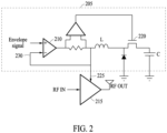
- FIG. 2 is a diagram illustrating envelope tracking (ET) switching noise caused when supplying power based on ET of a radio frequency (RF) signal in a communication apparatus (not shown) (e.g., the electronic device 101 of FIG. 1 ) according to one example embodiment.
- ET envelope tracking
- a power modulator 205 included in the communication apparatus (not shown) and an amplifier 215 for amplifying the RF signal by receiving power from the power modulator 205.
- the RF signal amplified by the amplifier 215 may be a signal transmitted from the communication apparatus to the outside and may include data transmitted through a physical uplink shared channel (PUSCH).
- PUSCH physical uplink shared channel
- the communication apparatus may supply power to the amplifier 215 in various power supply modes.
- the communication apparatus may supply predetermined voltage or supply power to the amplifier 215 in an ET mode, which is a power supply mode for supplying power based on ET of the RF signal, or in an average power tracking (APT) mode, which is a power supply mode for supplying power based on average power of the RF signal to increase power efficiency.
- ET mode which is a power supply mode for supplying power based on ET of the RF signal
- APT average power tracking
- the power modulator 205 may supply power to the amplifier 215 in the ET mode.
- the power modulator 205 may include an amplifier 210 for receiving and amplifying an envelope signal of an RF signal, a switch 220 that is on and off based on an output of the amplifier 210, a capacitor C that is charged and discharged based on the on and off of the switch 220, and an inductor L for supplying power charged and discharged in the capacitor C to the amplifier 215.
- the envelope signal of an RF signal may be input to the power modulator 205, and the input envelope signal may be amplified by the amplifier 210 of the power modulator 205.
- the amplifier 210 may be a linear amplifier.
- the switch 220 may be on and off based on an output of the amplifier 210, and output power of the power modulator 205 may be supplied to the amplifier 215 through the inductor L.
- Output voltage 225 of the power modulator 205 may be provided back as a differential input 230 of the amplifier 210. A difference between the voltage of the envelope signal input to the amplifier 210 and the output voltage 225 of the power modulator 205 may be reflected, as an error, in the output of the amplifier 210.
- the switch 220 may be repeatedly on and off based on the output of the amplifier 210 and may output voltage in a rectangular waveform.
- the rectangular-waveform voltage may cause ET switching noise.
- the ET switching noise may be applied to a reception port of an RFIC of the communication apparatus through front-end configuration, such as a duplexer, a low-noise amplifier (LNA), and a surface acoustic wave (SAW) filter of the communication apparatus, and may decrease the reception performance of the communication apparatus at maximum power.
- front-end configuration such as a duplexer, a low-noise amplifier (LNA), and a surface acoustic wave (SAW) filter of the communication apparatus, and may decrease the reception performance of the communication apparatus at maximum power.
- the ET switching noise may affect the reception performance more in a certain communication band than other bands.
- the ET switching noise may affect the reception performance more in a communication band where an interval between an uplink band and a downlink band is relatively narrow.
- LTE long-term evolution
- the ET switching noise may further affect the reception performance.
- the communication apparatus may supply power to the amplifier 215 by using the APT mode, but power efficiency may decrease.
- a method of controlling power supply for amplifying an RF signal and a communication apparatus for performing the same may control an increase in power consumption when using an APT mode by setting a condition for switching between an ET mode and the APT mode.
- FIG. 3 is a block diagram illustrating a communication apparatus according to one example embodiment.
- a communication apparatus 300 may include an amplifier 320 for amplifying an RF signal transmitted to the outside through an antenna, a power modulator 315 for supplying power to the amplifier 320, and a processor 305 for controlling the power modulator 315.
- the processor 305 may include a communication processor for processing a digital signal.
- the communication apparatus 300 may process a transmitted or received RF signal and may include an RFIC 310 for performing conversion between analog and digital signals.
- the communication apparatus 300 may include a front-end circuit (not shown) for preprocessing an RF signal converted into an analog signal by the RFIC 310, and the front-end circuit may include the amplifier 320.
- the power modulator 315 may supply power to the amplifier 320 in an APT or ET mode.
- a circuit of the power modulator 315 is illustrated as an example.
- the power modulator 315 may include a first buck converter 325 for supplying power to the amplifier 320 in the APT mode.
- the first buck converter 325 may be a buck boost converter.
- the power modulator 315 may include at least one linear amplifier for supplying power in the ET mode.
- the power modulator 315 may include a first linear amplifier 330 for converting power for 3-generation (3G) communication and LTE communication and a second linear amplifier 335 for converting power for 5G communication and 5G Sub-6 communication.
- the power modulator 315 may include a second buck converter 340, which slowly operates compared to the first linear amplifier 330.
- the configuration of the circuit of the power modulator 315 illustrated in FIG. 3 is merely an example, and the power modulator 315 may be variously configured.
- the amplifier 320 may include at least one amplifier based on the frequency feature of an RF signal to be amplified.
- the processor 305 may determine a power supply mode with respect to the amplifier 320 between any one of the APT mode and the ET mode, and based on the determined mode, may control the power modulator 315.
- BLER block error rate
- the processor 305 may determine whether the power supply mode for supplying power to the amplifier 320 from the power modulator 315 is the ET mode.
- the processor 305 when the power supply mode is the ET mode, may determine whether a downlink BLER in the ET mode and a downlink modulation method in the ET mode satisfy a first condition.
- the processor 305 when the first condition is satisfied, may determine whether a full resource block (RB) in an uplink band is allocated to uplink data transmission.
- the processor 305 when the full RB in the uplink band is allocated to the uplink data transmission, may switch the power supply mode to the APT mode.
- RB resource block
- the first condition may include a condition whether the downlink BLER in the ET mode is greater than or equal to a first reference downlink BLER corresponding to the downlink modulation method in the ET mode.
- a downlink modulation method such as quadrature phase shift keying (QPSK), 16-quadrature amplitude modulation (16-QAM), 64- QAM, and/or 256-QAM, may be used as the downlink modulation method in the ET mode for an RF signal
- the first condition may include a condition on the first reference downlink BLER corresponding to the downlink modulation method usable in the ET mode.
- the processor 305 may determine that the first condition is satisfied.
- the first reference downlink BLER corresponding to the downlink modulation method in the ET mode in the first condition may be the same or differ depending on which downlink modulation method is used. For example, when the QPSK, 16-QAM, 64-QAM, or 256-QAM downlink modulation method is used in the ET mode, the first reference downlink BLER corresponding to the QPSK, 16-QAM, and 64-QAM downlink modulation methods in the first condition may be about 3%, and the first reference downlink BLER corresponding to the 256-QAM downlink modulation method may be about 5%.
- the first reference downlink BLER corresponding to the QPSK and 16-QAM downlink modulation methods may be about 3% and the first reference downlink BLER corresponding to the 64-QAM and 256-QAM downlink modulation methods may be about 5%.
- the first reference downlink BLER corresponding to the QPSK, 16-QAM, 64-QAM, and 256-QAM downlink modulation methods may be about 5%.
- the first reference downlink BLER corresponding to the QPSK, 16-QAM, 64-QAM, and 256-QAM downlink modulation methods may be about 2%, 3%, 4%, and 5%, respectively.
- a downlink BLER may vary depending on a downlink modulation method.
- the downlink BLER may increase as the number of symbols used in downlink modulation increases.
- a symbol may be a unit representing the number of bits transmitted once in a modulation process.
- 16-QAM may modulate an RF signal by using 16 symbols
- 64-QAM may modulate an RF signal by using 64 symbols.
- the first reference downlink BLER corresponding to the downlink modulation method in the ET mode in the first condition may have a greater value as more symbols are used in the downlink modulation method in the ET mode.
- the downlink BLER may increase sequentially from QPSK to 16-QAM, 64-QAM, and 256-QAM.
- the 256-QAM downlink modulation method in the ET mode may frequently exceed the first reference downlink BLER of about 3% corresponding to the downlink BLER in the ET mode. Therefore, a greater value (e.g., 5%) than the first reference downlink BLER of the QPSK, 16-QAM, and 64-QAM downlink modulation methods may be desirable to be the first reference downlink BLER corresponding to the 256-QAM downlink modulation method.
- the downlink modulation methods provided herein and the first reference downlink BLER value corresponding to each downlink modulation method may only be an example for describing the first condition.
- the first condition may include a condition on various downlink modulation methods and a first reference downlink BLER on each downlink modulation method.
- the processor 305 when the first condition is satisfied, may determine whether a full RB in an uplink band is allocated to uplink data transmission.
- the RB may refer to an allocable unit of frequency and may have a designated bandwidth.
- the uplink band may be divided into a plurality of RBs and may be allocated to the uplink data transmission in RB units.
- an uplink band with a 20 MHz bandwidth may be divided into 100 RBs, and the divided 100 RBs may be completely or partially allocated to the uplink data transmission.
- ET switching noise occurring in the ET mode may affect more the reception performance of the communication apparatus 300 than when a partial RB in the uplink band is allocated to the uplink data transmission.
- the communication apparatus 300 uses a B5 band of LTE communication including an uplink band of about 824 MHz to 849 MHz and a downlink band of about 869 MHz to 894 MHz
- 849 MHz frequency which is near the downlink band, may be used. Accordingly, ET switching noise may have a great impact on reception performance in the downlink band.
- a frequency of which the uplink band is relatively far from the downlink band may be used. Accordingly, ET switching noise may have a relatively small impact on the reception performance in the downlink band.
- the processor 305 since the ET switching noise may have a great impact on the reception performance when the full RB in the uplink band is allocated to the uplink data transmission, may switch the power supply mode to the APT mode. For example, when the uplink band is 20 MHz, the processor 305 may switch the power supply mode to the APT mode when 100 RBs are completely allocated to the uplink data transmission.
- the processor 305 when a partial RB, not the full RB, in the uplink band is allocated to the uplink data transmission, may compare a downlink BLER in the APT mode to a downlink BLER in the ET mode.
- the processor 305 may compare the downlink BLER in the APT mode with the downlink BLER in the ET mode through a physical uplink control channel (PUCCH).
- PUCCH physical uplink control channel
- the processor 305 when the downlink BLER in the APT mode is less than the downlink BLER in the ET mode, may switch the power supply mode to the APT mode.
- the processor 305 may determine whether to switch from the ET mode to the APT mode. Accordingly, the processor 305 may reduce the number of times switching to the APT mode, additional power consumed by using the APT mode, and deterioration of reception performance and downlink throughput (T-PUT) performance.
- the processor 305 may identify the downlink BLER in the ET mode and the downlink modulation method in the ET mode, and determine whether the downlink BLER in the ET mode and the downlink modulation method in the ET mode satisfy a second condition.
- the processor 305 may identify the downlink BLER in the ET mode and the downlink modulation method in the ET mode through the PUCCH.
- the second condition may include a condition whether the downlink BLER in the ET mode is less than a second reference downlink BLER corresponding to the downlink modulation method in the ET mode.
- the second condition may include a condition on a second reference downlink BLER corresponding to the downlink modulation method that may be used in the ET mode.
- the processor 305 when the downlink BLER in the ET mode is less than the second reference downlink BLER corresponding to the downlink modulation method used in the ET mode, may determine that the second condition is satisfied.
- the second reference downlink BLER may be a downlink BLER less than the first reference downlink BLER by a threshold value (e.g., 2% or other designated vales).
- the threshold value may be set to prevent frequent switching between the ET mode and the APT mode.
- the second condition corresponding to the first condition in Table 1 is provided as an example.
- the first downlink BLER corresponding to the QPSK, 16-QAM, and 64-QAM downlink modulation methods is about 3%
- the first reference downlink BLER corresponding to the 256-QAM downlink modulation method is about 5%
- the second downlink BLER corresponding to the QPSK, 16-QAM, and 64-QAM downlink modulation methods may be about 1%
- the second reference downlink BLER corresponding to the 256-QAM downlink modulation method may be about 3%.
- the second downlink BLER corresponding to the QPSK and 16-QAM downlink modulation methods may be about 1%, and the second reference downlink BLER corresponding to the 64-QAM and 256-QAM downlink modulation methods may be about 3%.
- the first reference downlink BLER corresponding to the QPSK, 16-QAM, 64-QAM, and 256-QAM downlink modulation methods when, in the first condition, the first reference downlink BLER corresponding to the QPSK, 16-QAM, 64-QAM, and 256-QAM downlink modulation methods is about 5%, in the second condition, the second reference downlink BLER corresponding to the QPSK, 16-QAM, 64-QAM, and 256-QAM downlink modulation methods may be about 3%.
- the first reference downlink BLER corresponding to the QPSK, 16-QAM, 64-QAM, and 256-QAM downlink modulation methods is about 2%, 3%, 4%, and 5%, respectively
- the second reference downlink BLER corresponding to the QPSK, 16-QAM, 64-QAM, and 256-QAM downlink modulation methods may be about 1%, 2%, 3%, and 4%, respectively.
- the downlink modulation methods provided herein and the second reference downlink BLER value corresponding to each downlink modulation method may only be an example for describing the second condition.
- the second condition may include a condition on various downlink modulation methods and a second reference downlink BLER on each downlink modulation method.
- the processor 305 when the second condition is not satisfied, may periodically identify, through the PUCCH, the downlink BLER in the ET mode and the downlink modulation method in the ET mode and may determine whether the downlink BLER in the ET mode and the downlink modulation method in the ET mode satisfy the second condition.
- the processor 305 when the second condition is satisfied, may switch the power supply mode to the ET mode.
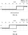
- FIGS. 4A and 4B are diagrams illustrating a condition on a downlink BLER and a downlink modulation method in a power supply control method according to one example embodiment.
- FIGS. 4A and 4B illustrate an example of switching a power supply mode in the first condition in Table 1 and the second condition in Table 2 provided as examples with reference to FIG. 3 .
- a processor e.g., the processor 305 of FIG. 3
- a processor may determine that the first condition is satisfied and switch the power supply mode from the ET mode to the APT mode.
- the processor 305 when the downlink BLER is greater than or equal to the first reference downlink BLER of about 5%, may determine that a second condition is satisfied and switch the power supply mode from the ET mode to the APT mode.
- the downlink BLER may increase as the number of symbols used in downlink modulation, and when applying the same first reference downlink BLER of about 3% to the QPSK, 16-QAM, 64-QAM, and 256-QAM, the 256-QAM downlink modulation method in the ET mode may frequently exceed the first reference downlink BLER of about 3% corresponding to the downlink BLER in the ET mode. Therefore, a greater value (e.g., 5%) than the first reference downlink BLER of the QPSK, 16-QAM, and 64-QAM downlink modulation methods may be desirable to be the first reference downlink BLER corresponding to the 256-QAM downlink modulation method.
- a greater value e.g., 5%
- the processor 305 may identify, through a PUCCH, in the APT mode, the downlink BLER in the ET mode and the downlink modulation method in the ET mode and may determine whether the downlink BLER in the ET mode and the downlink modulation method in the ET mode satisfy a second condition.
- the processor 305 when the downlink BLER is less than the second reference downlink BLER of about 1%, may determine that the second condition is satisfied and switch the power supply mode from the APT mode to the ET mode.
- the processor 305 when the downlink BLER is less than the second reference downlink BLER of about 3%, may determine that the second condition is satisfied and switch the power supply mode from the APT mode to the ET mode.
- the second reference downlink BLER may be a downlink BLER less than the first reference downlink BLER by a threshold value (e.g., 2% or other designated vales).
- the threshold value may be set to prevent frequent switching between the ET mode and the APT mode.
- the threshold value of about 2% is merely an example.
- a threshold value between the first reference downlink BLER and the second reference downlink BLER may be set variously.
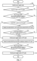
- FIG. 5 is a flowchart illustrating a power supply control method according to one example embodiment.
- a communication apparatus e.g., the communication apparatus of FIG. 3
- the communication apparatus 300 may identify the power supply mode for supplying power again.
- the communication apparatus 300 when the power supply mode is the ET mode, may determine whether a downlink BLER in the ET mode and a downlink modulation method in the ET mode satisfy a first condition.
- the communication apparatus 300 when the downlink BLER in the ET mode is greater than or equal to a first reference downlink BLER corresponding to the downlink modulation method used in the ET mode, may determine that the first condition is satisfied. The descriptions on the first condition provided with reference to FIG. 3 and FIG. 4a are not repeated.
- the communication apparatus 300 may identify the power supply mode for supplying power again.
- the communication apparatus 300 may determine whether a full RB in an uplink band is allocated to the uplink data transmission.
- the communication apparatus 300 may switch the power supply mode to the APT mode in operation 535.
- the communication apparatus 300 may identify, through a PUCCH, a downlink BLER in an APT mode and the downlink BLER in the ET mode, and in operation 530, may determine whether the downlink BLER in the APT mode is less than the downlink BLER in the ET mode.
- the communication apparatus 300 may identify the power supply mode for supplying power again.
- the communication apparatus 300 may switch the power supply mode to the APT mode.
- the communication apparatus 300 may determine whether to switch from the ET mode to the APT mode. Accordingly, the communication apparatus 300 may reduce the number of times switching to the APT mode and additional power consumed by using the APT mode.
- the communication apparatus 300 may identify the downlink BLER in the ET mode and the downlink modulation method in the ET mode through the PUCCH, and in operation 545, may determine whether the downlink BLER in the ET mode and the downlink modulation method in the ET mode satisfy a second condition.
- the communication apparatus 300 when the downlink BLER in the ET mode is less than a second reference downlink BLER corresponding to the downlink modulation method used in the ET mode, may determine that the second condition is satisfied. The descriptions on the second condition provided with reference to FIG. 3 and FIG. 4b are not repeated.
- the communication apparatus 300 may identify, through the PUCCH, the downlink BLER in the ET mode and the downlink modulation method in the ET mode again.
- the communication apparatus 300 in operation 550 may switch the power supply mode to the ET mode.
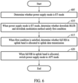
- FIG. 6 is a flowchart illustrating a power supply control method according to one example embodiment.
- the power supply control method may include: determining whether a power supply mode for supplying power from a power modulator 315 of a communication apparatus 300 to an amplifier 320 for amplifying an RF signal is an ET mode for supplying the power based on the ET of the RF signal in operation 605; when the power supply mode is the ET mode, determining whether a downlink BLER in the ET mode and a downlink modulation method in the ET mode satisfy a first condition in operation 610; when the first condition is satisfied, determining whether a full RB in an uplink band is allocated to uplink data transmission in operation 615; and when the full RB in the uplink band is allocated to the uplink data transmission, switching the power supply mode to an APT mode for supplying power based on average power of the RF signal in operation 620.
- Operation 605 may include operations 505 and 510 of FIG. 5 .
- Operation 610 may correspond to operation 515 of FIG. 5 .
- Operation 615 may correspond to operation 520 of FIG. 5 .
- Operation 620 may correspond to operation 535 of FIG. 5 .
- the power supply control method when a partial RB in the uplink band is allocated to uplink data transmission, may further include: comparing a downlink BLER in the APT mode with the downlink BLER in the ET mode; and when the downlink BLER in the APT mode is less than the downlink BLER in the ET mode, switching the power supply mode to the APT mode.
- the power supply control method may further include: determining, in the APT mode, whether the downlink BLER in the ET mode and the downlink modulation method in the ET mode satisfy a second condition; and when the second condition is satisfied, switching the power supply mode to the ET mode.
- the first condition may include a condition whether the downlink BLER in the ET mode is greater than or equal to a first reference downlink BLER corresponding to the downlink modulation method in the ET mode, and the determining whether the first condition is satisfied may include determining that the first condition is satisfied when the downlink BLER in the ET mode is greater than or equal to the first reference downlink BLER corresponding to the downlink modulation method in the ET mode.
- the second condition may include a condition on whether the downlink BLER in the ET mode is less than a second reference downlink BLER corresponding to the downlink modulation method in the ET mode, and the determining whether the second condition is satisfied may include determining that the second condition is satisfied when the downlink BLER in the ET mode is less than the second reference downlink BLER corresponding to the downlink modulation method in the ET mode.
- the second reference downlink BLER may be a downlink BLER less than the first reference downlink BLER by a threshold value.
- the comparing the downlink block error rate in the APT mode with the downlink block error rate in the ET mode may be performed through a PUCCH.
- the RF signal may include data transmitted through a PUSCH.
- the first reference downlink BLER corresponding to the downlink modulation method in the ET mode in the first condition may have a greater value as more symbols are used in the downlink modulation method in the ET mode.
- a communication apparatus 300 may include an amplifier 320 for amplifying an RF signal, a power modulator 315 for supplying power to the amplifier 320, and a processor 305 for controlling the power modulator 315,
- the processor 305 may determine whether a power supply mode for supplying the power from the power modulator 315 to the amplifier 320 is an ET mode for supplying the power based on ET of the RF signal, when the power supply mode is the ET mode, determine whether a downlink BLER in the ET mode and a downlink modulation method in the ET mode satisfy a first condition, when the first condition is satisfied, determine whether a full RB in an uplink band is allocated to uplink data transmission, and when the full RB in the uplink band is allocated to the uplink data transmission, switch the power supply mode to an APT mode for supplying the power based on average power of the RF signal.
- the processor 305 when a partial RB in the uplink band is allocated to uplink data transmission, may compare a downlink BLER in the APT mode with the downlink BLER in the ET mode, and when the downlink BLER in the APT mode is less than the downlink BLER in the ET mode, switch the power supply mode to the APT mode.
- the processor 305 may determine, in the APT mode, whether the downlink BLER in the ET mode and the downlink modulation method in the ET mode satisfy the second condition, and when the second condition is satisfied, switch the power supply mode to the ET mode.
- the first condition may include a condition on whether the downlink BLER in the ET mode is greater than or equal to a first reference downlink BLER corresponding to the downlink modulation method in the ET mode, and the processor 305 may determine that the first condition is satisfied when the downlink BLER in the ET mode is greater than or equal to the first reference downlink BLER corresponding to the downlink modulation method in the ET mode.
- the second condition may include a condition on whether the downlink BLER in the ET mode is less than a second reference downlink BLER corresponding to the downlink modulation method in the ET mode, and the processor 305 may determine that the second condition is satisfied when the downlink BLER in the ET mode is less than the second reference downlink BLER corresponding to the downlink modulation method in the ET mode.
- the second reference downlink BLER may be a downlink BLER less than the first reference downlink BLER by a threshold value.
- the processor 305 may compare the downlink BLER in the APT mode with the downlink BLER in the ET mode through a PUCCH.
- the RF signal may include data transmitted through a PUSCH.
- the first reference downlink BLER corresponding to the downlink modulation method in the ET mode in the first condition may have a greater value as more symbols are used in the downlink modulation method in the ET mode.
- the processor 305 when the second condition is not satisfied, in the APT mode, periodically perform the determining whether the downlink BLER in the ET mode and the downlink modulation method in the ET mode satisfy the second condition.
- the electronic device may be one of various types of electronic devices.
- the electronic device may include, for example, a portable communication device (e.g., a smartphone), a computer device, a portable multimedia device, a portable medical device, a camera, a wearable device, or a home appliance device.
- a portable communication device e.g., a smartphone
- a computer device e.g., a laptop, a desktop, a tablet, or a portable multimedia device.
- a portable medical device e.g., a portable medical device
- camera e.g., a portable medical device
- a camera e.g., a camera
- a wearable device e.g., a portable medical device
- a home appliance device e.g., a portable medical device, a portable medical device, a camera, a wearable device, or a home appliance device.
- the electronic device is not limited to those described above.
- a or B at least one of A and B, “at least one of A or B”, “A, B or C”, “at least one of A, B and C", and “A, B, or C,” each of which may include any one of the items listed together in the corresponding one of the phrases, or all possible combinations thereof.
- Terms such as “first”, “second”, or “first” or “second” may simply be used to distinguish the component from other components in question, and do not limit the components in other aspects (e.g., importance or order).
- an element e.g., a first element
- the element may be coupled with the other element directly (e.g., by wire), wirelessly, or via a third element.
- module may include a unit implemented in hardware, software, or firmware, and may interchangeably be used with other terms, for example, “logic,” “logic block,” “part,” or “circuitry”.
- a module may be a single integral component, or a minimum unit or part thereof, adapted to perform one or more functions.
- the module may be implemented in a form of an application-specific integrated circuit (ASIC).
- ASIC application-specific integrated circuit
- Various example embodiments as set forth herein may be implemented as software (e.g., the program 140) including one or more instructions that are stored in a storage medium (e.g., the internal memory 136 or the external memory 138) that is readable by a machine (e.g., the electronic device 101).
- a processor e.g., the processor 120
- the one or more instructions may include code generated by a compiler or code executable by an interpreter.
- the machine-readable storage medium may be provided in the form of a non-transitory storage medium.
- non-transitory simply means that the storage medium is a tangible device, and does not include a signal (e.g., an electromagnetic wave), but this term does not differentiate between where data is semi-permanently stored in the storage medium and where the data is temporarily stored in the storage medium.
- a method may be included and provided in a computer program product.
- the computer program product may be traded as a product between a seller and a buyer.
- the computer program product may be distributed in the form of a machine-readable storage medium (e.g., a compact disc read-only memory (CD-ROM)), or be distributed (e.g., downloaded or uploaded) online via an application store (e.g., PlayStore TM ), or between two user devices (e.g., smartphones) directly. If distributed online, at least part of the computer program product may be temporarily generated or at least temporarily stored in the machine-readable storage medium, such as a memory of the manufacturer's server, a server of the application store, or a relay server.
- each component e.g., a module or a program of the above-described components may include a single entity or multiple entities, and some of the multiple entities may be separately disposed in different components. According to various example embodiments, one or more of the above-described components may be omitted, or one or more other components may be added. Alternatively or additionally, a plurality of components (e.g., modules or programs) may be integrated into a single component. In such a case, according to various example embodiments, the integrated component may still perform one or more functions of each of the plurality of components in the same or similar manner as they are performed by a corresponding one of the plurality of components before the integration.
- the integrated component may still perform one or more functions of each of the plurality of components in the same or similar manner as they are performed by a corresponding one of the plurality of components before the integration.
- operations performed by the module, the program, or another component may be carried out sequentially, in parallel, repeatedly, or heuristically, or one or more of the operations may be executed in a different order or omitted, or one or more other operations may be added.
Landscapes
- Engineering & Computer Science (AREA)
- Computer Networks & Wireless Communication (AREA)
- Signal Processing (AREA)
- Quality & Reliability (AREA)
- Power Engineering (AREA)
- Mobile Radio Communication Systems (AREA)
- Transmitters (AREA)
Applications Claiming Priority (3)
| Application Number | Priority Date | Filing Date | Title |
|---|---|---|---|
| KR20210157488 | 2021-11-16 | ||
| KR1020220000231A KR20230071675A (ko) | 2021-11-16 | 2022-01-03 | Rf 신호 증폭을 위한 전력 공급 제어 방법 및 이를 수행하는 통신 장치 |
| PCT/KR2022/016773 WO2023090689A1 (ko) | 2021-11-16 | 2022-10-30 | Rf 신호 증폭을 위한 전력 공급 제어 방법 및 이를 수행하는 통신 장치 |
Publications (1)
| Publication Number | Publication Date |
|---|---|
| EP4366174A1 true EP4366174A1 (de) | 2024-05-08 |
Family
ID=86323320
Family Applications (1)
| Application Number | Title | Priority Date | Filing Date |
|---|---|---|---|
| EP22895896.3A Pending EP4366174A1 (de) | 2021-11-16 | 2022-10-30 | Verfahren zur steuerung der stromversorgung zur hf-signalverstärkung und kommunikationsvorrichtung zur durchführung davon |
Country Status (2)
| Country | Link |
|---|---|
| US (1) | US20230156613A1 (de) |
| EP (1) | EP4366174A1 (de) |
-
2022
- 2022-10-30 EP EP22895896.3A patent/EP4366174A1/de active Pending
- 2022-12-22 US US18/086,642 patent/US20230156613A1/en active Pending
Also Published As
| Publication number | Publication date |
|---|---|
| US20230156613A1 (en) | 2023-05-18 |
Similar Documents
| Publication | Publication Date | Title |
|---|---|---|
| US11588443B2 (en) | Method and device for selectively supplying voltage to multiple amplifiers by using switching regulators | |
| US20220368358A1 (en) | Electronic device including power amplifier and front-end module including power amplifier | |
| US20230040041A1 (en) | Electronic device for transmitting radio-frequency signal and method for operating same | |
| EP4366174A1 (de) | Verfahren zur steuerung der stromversorgung zur hf-signalverstärkung und kommunikationsvorrichtung zur durchführung davon | |
| US20230081582A1 (en) | Electronic device and method for controlling power supplied to transmit signal | |
| US11784676B2 (en) | Method of switching receiving path and electronic device therefor | |
| US20230007836A1 (en) | Wireless communication device including radio frequency integrated circuit and method of controlling the same | |
| US20240171135A1 (en) | Communication circuit including amplifier module, and electronic device comprising same | |
| US20220369234A1 (en) | Electronic device and method for adjusting output power of radio frequency signal to be output to antenna | |
| US11909435B2 (en) | Method for multi-band communication and electronic device thereof | |
| US20230126353A1 (en) | Communication circuitry including amplifying module and an electronic device including the communication circuitry | |
| US20240039489A1 (en) | Electronic device comprising power amplifier and method for operating same | |
| US20240204820A1 (en) | Electronic device for controlling output of power amplifier | |
| US11855481B2 (en) | Electronic device including power management integrated circuit and operating method thereof | |
| US20230353172A1 (en) | Electronic device and method for controlling transmission power of communication module | |
| US20230126162A1 (en) | Multiplexer and electronic device containing multiplexer | |
| US20230327612A1 (en) | Communication circuit including amplifier module, and electronic device comprising same | |
| EP4336734A1 (de) | Elektronische vorrichtung zur einstellung der empfangsverstärkung für ein hf-signal auf basis von 2 sendebetrieb und steuerungsverfahren dafür | |
| US20230103900A1 (en) | Electronic device and method for improving thermal performance thereof | |
| US20230412200A1 (en) | Communication circuitry for preventing loss of received signals, and electronic device comprising same | |
| US20230345443A1 (en) | Electronic device including antenna module in communication system, and method of operating same | |
| US20240276402A1 (en) | Electronic device comprising multi-sim | |
| US20240056146A1 (en) | Electronic device for transmitting srs and an operation method thereof | |
| EP4351021A1 (de) | Elektronische vorrichtung zur identifizierung des zustands einer schaltung im zusammenhang mit kommunikation | |
| US20240030960A1 (en) | Electronic device and harmonic control method of electronic device |
Legal Events
| Date | Code | Title | Description |
|---|---|---|---|
| STAA | Information on the status of an ep patent application or granted ep patent |
Free format text: STATUS: THE INTERNATIONAL PUBLICATION HAS BEEN MADE |
|
| PUAI | Public reference made under article 153(3) epc to a published international application that has entered the european phase |
Free format text: ORIGINAL CODE: 0009012 |
|
| STAA | Information on the status of an ep patent application or granted ep patent |
Free format text: STATUS: REQUEST FOR EXAMINATION WAS MADE |
|
| 17P | Request for examination filed |
Effective date: 20240202 |
|
| AK | Designated contracting states |
Kind code of ref document: A1 Designated state(s): AL AT BE BG CH CY CZ DE DK EE ES FI FR GB GR HR HU IE IS IT LI LT LU LV MC ME MK MT NL NO PL PT RO RS SE SI SK SM TR |