EP4366163A2 - Differentielle allpass-koppelschaltung mit gleichtaktrückkopplung - Google Patents
Differentielle allpass-koppelschaltung mit gleichtaktrückkopplung Download PDFInfo
- Publication number
- EP4366163A2 EP4366163A2 EP23207140.7A EP23207140A EP4366163A2 EP 4366163 A2 EP4366163 A2 EP 4366163A2 EP 23207140 A EP23207140 A EP 23207140A EP 4366163 A2 EP4366163 A2 EP 4366163A2
- Authority
- EP
- European Patent Office
- Prior art keywords
- voltage
- common mode
- input
- switch
- output
- Prior art date
- Legal status (The legal status is an assumption and is not a legal conclusion. Google has not performed a legal analysis and makes no representation as to the accuracy of the status listed.)
- Pending
Links
Images






Classifications
-
- H—ELECTRICITY
- H03—ELECTRONIC CIRCUITRY
- H03F—AMPLIFIERS
- H03F3/00—Amplifiers with only discharge tubes or only semiconductor devices as amplifying elements
- H03F3/45—Differential amplifiers
- H03F3/45071—Differential amplifiers with semiconductor devices only
- H03F3/45479—Differential amplifiers with semiconductor devices only characterised by the way of common mode signal rejection
- H03F3/45928—Differential amplifiers with semiconductor devices only characterised by the way of common mode signal rejection using IC blocks as the active amplifying circuit
- H03F3/45932—Differential amplifiers with semiconductor devices only characterised by the way of common mode signal rejection using IC blocks as the active amplifying circuit by using feedback means
-
- H—ELECTRICITY
- H03—ELECTRONIC CIRCUITRY
- H03F—AMPLIFIERS
- H03F3/00—Amplifiers with only discharge tubes or only semiconductor devices as amplifying elements
- H03F3/45—Differential amplifiers
- H03F3/45071—Differential amplifiers with semiconductor devices only
- H03F3/45076—Differential amplifiers with semiconductor devices only characterised by the way of implementation of the active amplifying circuit in the differential amplifier
- H03F3/45475—Differential amplifiers with semiconductor devices only characterised by the way of implementation of the active amplifying circuit in the differential amplifier using IC blocks as the active amplifying circuit
-
- H—ELECTRICITY
- H03—ELECTRONIC CIRCUITRY
- H03F—AMPLIFIERS
- H03F1/00—Details of amplifiers with only discharge tubes, only semiconductor devices or only unspecified devices as amplifying elements
- H03F1/26—Modifications of amplifiers to reduce influence of noise generated by amplifying elements
-
- H—ELECTRICITY
- H03—ELECTRONIC CIRCUITRY
- H03F—AMPLIFIERS
- H03F3/00—Amplifiers with only discharge tubes or only semiconductor devices as amplifying elements
- H03F3/189—High-frequency amplifiers, e.g. radio frequency amplifiers
- H03F3/19—High-frequency amplifiers, e.g. radio frequency amplifiers with semiconductor devices only
- H03F3/195—High-frequency amplifiers, e.g. radio frequency amplifiers with semiconductor devices only in integrated circuits
-
- H—ELECTRICITY
- H04—ELECTRIC COMMUNICATION TECHNIQUE
- H04L—TRANSMISSION OF DIGITAL INFORMATION, e.g. TELEGRAPHIC COMMUNICATION
- H04L25/00—Baseband systems
- H04L25/02—Details ; arrangements for supplying electrical power along data transmission lines
- H04L25/0264—Arrangements for coupling to transmission lines
- H04L25/0272—Arrangements for coupling to multiple lines, e.g. for differential transmission
- H04L25/0276—Arrangements for coupling common mode signals
-
- H—ELECTRICITY
- H03—ELECTRONIC CIRCUITRY
- H03F—AMPLIFIERS
- H03F2203/00—Indexing scheme relating to amplifiers with only discharge tubes or only semiconductor devices as amplifying elements covered by H03F3/00
- H03F2203/45—Indexing scheme relating to differential amplifiers
- H03F2203/45084—Indexing scheme relating to differential amplifiers the common mode signal circuit comprising one or more inductive or capacitive elements, e.g. filter circuitry
-
- H—ELECTRICITY
- H03—ELECTRONIC CIRCUITRY
- H03F—AMPLIFIERS
- H03F2203/00—Indexing scheme relating to amplifiers with only discharge tubes or only semiconductor devices as amplifying elements covered by H03F3/00
- H03F2203/45—Indexing scheme relating to differential amplifiers
- H03F2203/45544—Indexing scheme relating to differential amplifiers the IC comprising one or more capacitors, e.g. coupling capacitors
-
- H—ELECTRICITY
- H03—ELECTRONIC CIRCUITRY
- H03F—AMPLIFIERS
- H03F2203/00—Indexing scheme relating to amplifiers with only discharge tubes or only semiconductor devices as amplifying elements covered by H03F3/00
- H03F2203/45—Indexing scheme relating to differential amplifiers
- H03F2203/45551—Indexing scheme relating to differential amplifiers the IC comprising one or more switched capacitors
-
- H—ELECTRICITY
- H03—ELECTRONIC CIRCUITRY
- H03F—AMPLIFIERS
- H03F2203/00—Indexing scheme relating to amplifiers with only discharge tubes or only semiconductor devices as amplifying elements covered by H03F3/00
- H03F2203/45—Indexing scheme relating to differential amplifiers
- H03F2203/45586—Indexing scheme relating to differential amplifiers the IC comprising offset generating means
Definitions
- the technology disclosed herein relates to signal processing, and in particular to a differential all-pass coupling circuit with common mode feedback.
- Receivers such as wireline signal receivers, are devices that may receive electromagnetic signals.
- the electromagnetic signals may include high-frequency and low-frequency signal components.
- Some wireline signal receivers may have alternating current (AC) coupling circuits to allow the high-frequency signal components to pass through a connection while the low-frequency signal components are attenuated.
- AC alternating current
- Some aspects relate to an apparatus comprising an anti-aliasing circuit configured to reduce a bandwidth of a first differential signal received from a termination circuit of a receiver; and a switched-capacitor circuit coupled to an output of the anti-aliasing circuit, the switched-capacitor circuit configured to: control a first switch to charge a capacitor to a first voltage, wherein the first voltage is based on a first difference between a common mode input voltage and a common mode reference voltage, the common mode input voltage associated with a first common mode voltage of the first differential signal, the common mode reference voltage associated with a second common mode voltage of an input stage of the receiver; control a second switch to provide a second voltage to the capacitor, the second voltage based on a second difference between the first differential signal and the common mode input voltage; and output a second differential signal to the input stage of the receiver, the second differential signal based on the first differential signal adjusted by the second voltage.
- Some aspects relate to another apparatus comprising coil circuitry configured to receive a first differential signal; input stage circuitry; and alternating current coupling circuitry coupled to an output of the coil circuitry, the alternating current coupling circuitry configured to: charge a capacitor to a first voltage, the first voltage based on a first difference between a common mode input voltage and a common mode reference voltage, the common mode input voltage associated with a first common mode voltage of the first differential signal, the common mode reference voltage associated with a second common mode voltage of the input stage circuitry; provide a second voltage to the capacitor, the second voltage based on a second difference between the first differential signal and the common mode input voltage; and output a second differential signal to the input stage circuitry, the second differential signal adjusted by the second voltage; and wherein the input stage circuitry is configured to convert the second differential signal to a third differential signal.
- Some aspects relate to a method comprising sensing an output common mode voltage associated with a differential signal of an input stage of a receiver; determining a difference between the sensed output common mode voltage and a target output common mode voltage; determining whether the difference satisfies a threshold; and in response to determining that the difference satisfies the threshold, outputting a voltage to an all-pass circuit to adjust the output common mode voltage.
- a data receiving device may include a receiver that uses a T-coil through which input data propagates.
- the T-coil may include two coils with a mutual inductance between them and configured for input bandwidth extension.
- the T-coil may output an alternating signal that includes high-frequency signal components and low-frequency signal components.
- Some receivers may use an alternating current (AC) coupling circuit to allow high-frequency signal components of a signal to pass to a differential amplifier (e.g., a fully differential amplifier) of the receivers and direct current (DC) and/or low-frequency signal components of the signal to be attenuated.
- AC alternating current
- an AC coupling circuit may be configured to operate as a high-pass filter to pass the high-frequency signal components to the differential amplifier and suppress the DC and/or low-frequency signal components.
- Common mode rejection refers to suppression of signals common to two inputs, such as differential inputs of a receiver.
- the AC coupling circuit may effectuate input DC common mode rejection by decoupling an input signal common mode, such as a common mode at terminals that receive a differential signal, from a receiver input common mode, such as a common mode at an input of the differential amplifier.
- Some receivers may use the AC coupling circuit to bias a component of the receivers, such as a differential amplifier, using common mode feedback.
- the AC coupling circuit may be configured to bias the differential amplifier at a particular common mode DC bias voltage such that the differential amplifier may amplify the differential signal as designed.
- the AC coupling circuit may compare the common mode input signal to a reference signal and generate the common mode DC bias voltage based on the comparison.
- the cut-off frequency (f_AC) of AC coupling needs to be low enough to avoid affecting signal frequency content yet high enough to attenuate the common mode input signal.
- the cut-off frequency is too low, which can allow an increased level of the common mode input signal to reach a receiver component (e.g., a differential amplifier) and thereby reduce the effectiveness of input DC common mode rejection.
- the cut-off frequency is too high, which can cut off signal frequency content of the differential input signal and thereby decrease the signal-to-noise (SNR) ratio associated with the differential input signal.
- the cut-off frequency typically selected for conventional receivers is approximately 50 kilohertz (kHz).
- the cut-off frequency may be implemented by using discrete passive components such as capacitors and resistors in a particular circuit arrangement.
- a cut-off frequency of approximately 50 kHz results in a substantially large physical area of a die of a chip, a printed circuit board (PCB), etc., that is consumed by the discrete passive components, which causes enlargement of a physical footprint of the receiver device that includes the chip, the PCB, etc.
- baseline wandering may refer to a differential input signal drifting towards the common mode of the receiver.
- a receiver in a data receiving device may receive data representing a relatively long string of zeros or ones such that the average power of the receiver may skew away from a baseline average power of the receiver. For example, the average power of the receiver may skew higher in response to receiving a relatively long string of ones and data representing zeros may be misinterpreted as ones due to the upshifted average power.
- Another challenge is reducing the supply voltage for operation of the receiver. For example, there is a substantially large voltage headroom across the above-referenced cascode current sources. A higher supply voltage is needed to provide such a large voltage headroom to control the high-voltage cascode current sources. A higher supply voltage may be detrimental in some receivers that are power constrained (e.g., a receiver powered by a battery).
- the inventors have recognized and appreciated that the above challenges have not been overcome by conventional AC coupling circuits, and/or, more generally, by conventional receivers.
- the inventors have developed a differential all-pass coupling circuit with common mode feedback to overcome the above challenges and improve upon conventional AC coupling and/or receiver circuits.
- the inventor's differential all-pass coupling circuit disclosed herein passes through a differential input signal and provides common mode feedback control all while supporting a wide voltage range with low power and low area overhead.
- the differential all-pass coupling circuit can be implemented at least in part using a switched-capacitor signal processing circuit to decouple a differential input signal from a DC signal.
- the switched-capacitor signal processing circuit can implement an effective switched-capacitor low-pass filter with an operating clock frequency designed for a particular AC coupling bandwidth.
- the substantial increase in AC coupling bandwidth overcomes the challenge of having the cut-off frequency being too low or too high.
- the increased AC coupling bandwidth can be substantially greater than the 50 kHz cut-off frequency of conventional AC coupling circuits.
- the increased AC coupling circuit can result in substantial reductions in die area and/or PCB area compared to conventional AC coupling circuits.
- the switched-capacitor signal processing circuit can utilize differential sampling to overcome the baseline wandering challenges described above.
- the inventor's switched-capacitor signal processing circuit disclosed herein can adjust a common mode of the differential input signal with a feedback signal to generate a desired common mode for a component of a receiver, such as a differential amplifier.
- the differential all-pass coupling circuit can utilize a dynamic comparator with logic-level feedback to generate the feedback signal.
- the switched-capacitor signal processing circuit can achieve accurate DC-coupling of differential input signals without using high-impedance cascode current sources and/or high-impedance bias voltage generation techniques.
- the switched-capacitor signal processing circuit can achieve accurate DC-coupling of differential input signals with a wide voltage range and low power overhead compared to conventional cascode-current source implementations.
- FIG. 1 is a schematic illustration of an example receiver system 100 to receive a differential signal from input terminals 102, 104 (identified by RXINP and RXINN, RXINP-RXINN, RXINP/RXINN, or RXINP/N).
- the receiver system 100 is a wireline receiver, such as a data communication wireline receiver.
- wireline receivers include Ethernet interfaces, Peripheral Component Interconnect (PCI) interfaces, Serial Digital Interfaces (SDI), Universal Serial Bus (USB) interfaces, and High-Definition Multimedia Interfaces (HDMI).
- PCI Peripheral Component Interconnect
- SDI Serial Digital Interfaces
- USB Universal Serial Bus
- HDMI High-Definition Multimedia Interfaces
- the receiver system 100 is a wireless receiver, such as a wireless charging receiver, which can convert received electromagnetic signals into DC signals for charging a device, such as a battery of an electronic device.
- a wireless receiver such as a wireless charging receiver
- Non-limiting examples of electronic devices include laptop computers, tablet computers, smartphones, and wearable devices (e.g., headphones, headsets, smartwatches, smart glasses, etc.).
- the receiver system 100 includes a T-coil circuit 106 (identified by T-COIL), a receiver (RX) termination circuit 108, an AC coupling circuit 110, and an RX input stage circuit 112.
- the receiver system 100 may not include one(s) of the T-coil circuit 106, the RX termination circuit 108, the AC coupling circuit 110, and/or the RX input stage circuit 112.
- output(s) of the T-coil circuit 106 is/are coupled to input(s) of the RX termination circuit 108.
- output(s) of the T-coil circuit 106 is/are coupled to input(s) of the RX termination circuit 108 through one or more electrical connections.
- Non-limiting examples of electrical connections include opto-isolators, pads, traces, wires, and vias.
- output(s) of the RX termination circuit 108 is/are coupled to input(s) of the AC coupling circuit 110.
- output(s) of the AC coupling circuit 110 is/are coupled to input(s) of the RX input stage circuit 112.
- the receiver system 100 is implemented by one or more integrated circuits (ICs) (e.g., one or more monolithic ICs, one or more chips).
- ICs integrated circuits
- the T-coil circuit 106, the RX termination circuit 108, the AC coupling circuit 110, and the RX input stage circuit 112 can be included in the same chip.
- one or more of the T-coil circuit 106, the RX termination circuit 108, the AC coupling circuit 110, and/or the RX input stage circuit 112 may be implemented by separate ICs.
- the T-coil circuit 106 can be implemented by a first chip
- the RX termination circuit 108 can be implemented by a second chip
- the AC coupling circuit 110 can be implemented by a third chip
- the RX input stage circuit 112 can be implemented by a fourth chip.
- one(s) of the T-coil circuit 106, the RX termination circuit 108, the AC coupling circuit 110, and/or the RX input stage circuit 112 can be combined using different combinations of chips.
- the T-coil circuit 106 and the RX termination circuit 108 can be implemented by a first chip and the AC coupling circuit 110 and the RX input stage circuit 112 can be implemented by a second chip, different from the first chip.
- Any other combinations of the T-coil circuit 106, the RX termination circuit 108, the AC coupling circuit 110, and/or the RX input stage circuit 112 into one or more ICs are contemplated.
- the receiver system 100 includes the input terminals 102, 104 to receive a differential signal (e.g., a differential signal of RXINP and RXINN (RXINP/RXINN))
- a differential signal e.g., a differential signal of RXINP and RXINN (RXINP/RXINN)
- the input terminals 102, 104 can be pads, leads, legs, or vias of IC(s), chip(s), PCB(s), etc., that implement the receiver system 100.
- the receiver system 100 does not include the input terminals 102, 104.
- the T-coil circuit 106 can include terminals that respectively couple to the input terminals 102, 104, which may be associated with a different IC, chip, or system.
- the receiver system 100 of the illustrated example includes the T-coil circuit 106 to convert electromagnetic signals received from the input terminals 102, 104 to alternating signals, which are output to the RX termination circuit 108.
- the T-coil circuit 106 can implement coil circuitry to convert the electromagnetic signals to the alternating signals.
- the T-coil circuit 106 includes a first pair of inductors 114a, 114b coupled to a first electrostatic discharge (ESD) diode 116.
- ESD electrostatic discharge
- the T-coil circuit 106 includes a second pair of inductors 118a, 118b coupled to a second ESD diode 120.
- a first inductor 114a of the first pair of inductors 114a, 114b is coupled to a first input terminal 102 (identified by RXINP) of the input terminals 102, 104.
- a first inductor 118a of the second pair of inductors 118a, 118b is coupled to a second input terminal 104 (identified by RXINN) of the input terminals, 102, 104.
- the first and second ESD diodes 116, 120 are diodes coupled to the inductors 114a, 114b, 118a, 118b in such an arrangement to provide ESD protection to the T-coil circuit 106, and/or, more generally, the receiver system 100.
- the inductors 114a, 114b, 118a, 118b create oscillating magnetic fields in response to the electromagnetic signals received from the input terminals 102, 104. In some embodiments, the inductors 114a, 114b, 118a, 118b convert the oscillating magnetic fields to alternating signals, which may have AC and/or DC components. In some embodiments, the inductors 114a, 114b, 118a, 118b output the alternating signals to the RX termination circuit 108.
- the receiver system 100 of the illustrated example includes the RX termination circuit 108 to prevent reflections of the alternating signals received from the T-coil circuit 106 back to the T-coil circuit 106.
- the T-coil circuit 106 and the RX termination circuit 108 can be configured to provide a matching network for the input channels RXINP and RXINN.
- the RX termination circuit 108 includes first resistors 122, 124 (identified by R) coupled in parallel to a first capacitor 126 (identified by C_CM).
- the first capacitor 126 may be a common mode (CM) capacitor, such as a capacitor that is configured to store a common mode voltage (e.g., a common mode input voltage) associated with the input terminals 102, 104.
- C_CM 126 may store a common mode voltage associated with the differential signal (RXINP/RXINN).
- the resistances of the first resistors 122, 124 are the same.
- the respective resistances of the first resistors 122, 124 can be 50 ohms ( ⁇ ).
- the first resistors 122, 124 may have any other resistance.
- the first resistors 122, 124 may have a different resistance from each other.
- the receiver system 100 of the illustrated example includes the AC coupling circuit 110 for input DC common mode rejection.
- the AC coupling circuit 110 can implement AC coupling circuitry to reject the input DC common mode.
- the AC coupling circuit 110 can be configured to decouple the input signal common mode from the RX input common mode.
- the input signal common mode can be represented by a voltage across C_CM 126.
- the voltage that is common to both input terminals 102, 104 may generate the voltage across C_CM 126.
- the RX input common mode can be represented by a voltage across the inputs of the RX input stage circuit 112.
- the AC coupling circuit 110 of the illustrated example includes second capacitors 128, 130 (e.g., blocking capacitors, DC blocking capacitors) (identified by C_AC) configured to decouple the input signal common mode from the RX input common mode.
- C_AC 128, 130 may block (e.g., reject) DC and/or low-frequency components of a differential signal received by the input terminals 102, 104 (e.g., a differential signal represented by RXINP/RXINN).
- the receiver system 100 of the illustrated example includes the AC coupling circuit 110 for common mode feedback, such as common mode feedback control.
- the AC coupling circuit 110 can receive a bias voltage 132 (identified by RX_INCM) that may be generated in response to a comparison of the common mode voltage (e.g., the voltage across C_CM 126) and a common mode reference voltage.
- the AC coupling circuit 110 can inject the bias voltage 132 into the inputs of the RX input stage circuit 112 via second resistors 134, 136 (identified by R_AC).
- R_AC 134, 136 are coupled in parallel with C_AC 128, 130 and the inputs of the RX input stage circuit 112.
- C_AC 128 is coupled in parallel with R_AC 134.
- R_AC 134 is coupled in parallel with a first input of a differential amplifier 138 of the RX input stage circuit 112.
- Rh is the resistance of one ofR_AC 134, 136, Cac is the capacitance of one of C_AC 128, 130, and CL represents the capacitive loading of the RX input stage circuit 112.
- the AC coupling circuit 110 attenuates an input signal having a frequency below f_AC.
- the AC coupling circuit 110 can be configured to use the bias voltage 132 to bias a component of the RX input stage circuit 112, such as the differential amplifier 138.
- the AC coupling circuit 110 can inject the bias voltage 132 into the inputs of the differential amplifier 138 to ensure that the input voltage of the differential amplifier 138 is maintained in a specified range.
- the differential amplifier 138 of this example is a fully differential amplifier.
- the RX input stage circuit 112 may be configured to use a different type of amplifier and/or a different number of amplifiers.
- the receiver system 100 includes the RX input stage circuit 112 to output a differential output signal based on a differential input signal.
- the differential output signal from the RX input stage circuit 112 can be provided to other circuitry for additional processing, such as converting the differential output signal into digital data (e.g., data representing a logic zero, data representing a logic one, Ethernet data, serial data, etc.) for use by a downstream device (e.g., a computer-hardware processor, a digital signal processor, a network interface device, etc.).
- FIG. 2 is a schematic illustration of an example implementation of an AC coupling circuit 200.
- the AC coupling circuit 200 can implement the AC coupling circuit 110 of FIG. 1 .
- the AC coupling circuit 200 of FIG. 2 is coupled to an example implementation of an RX termination circuit 202.
- the RX termination circuit 202 of this example includes first resistors 204, 206 (identified by Rterm) coupled together in series.
- Rterm 204, 206 are coupled in parallel to respective inputs that provide input signals 208, 210 (identified by RX_INP and RX_INN).
- a common mode input voltage 212 (identified by CM_IN) of the input signals 208, 210 is represented as a voltage between Rterm 204, 206.
- the input signals 208, 210 correspond to RXINP and RXINN of FIG. 1 , respectively.
- the RX termination circuit 202 of FIG. 2 can implement the RX termination circuit 108 of FIG. 1 .
- Rterm 204, 206 of FIG. 2 may correspond to R 122, 124 of FIG. 1 .
- CM_IN 212 may correspond to the voltage across C_CM 126 of FIG. 1 .
- the DC components of the input signals 208, 210 may be blocked by first capacitors 214, 216 (identified by C_AC).
- C_AC 214, 216 of FIG. 2 may correspond to C_AC 128, 130 of FIG. 1 .
- the AC components of the input signals 208, 210 may propagate through C_AC 214, 216 and output as output signals 218, 220 (identified by OUTP and OUTN).
- C_AC 214, 216 and second resistors 222, 224 (identified by R_AC) may establish a first-order high-pass filter.
- second capacitors 226, 228 (identified by CL), which are representative of the capacitive loading of additional circuitry, such as the RX input stage circuit 112 of FIG. 1 .
- the AC coupling circuit 200 of the illustrated example includes an all-pass circuit 230 to provide voltages Vx_P 232 and Vx_N 234 such that the following conditions are satisfied: (1) a differential signal (RX_INN-RX_INN) is passed through the AC coupling circuit 200 for frequencies up to approximately 10*f_AC such that:
- the all-pass circuit 230 can be an all-pass filter configured such that the differential signal is passed through the AC coupling circuit 200 without affecting the high-frequency components of the input signals 208, 210.
- the all-pass circuit 230 can be configured such that the common mode input of the RX input stage circuit 112 of FIG. 1 can be provided as feedback to generate RX_INCM 236.
- the all-pass circuit 230 includes an anti-aliasing low-pass filter 238 (identified by AA LPF) and a switched-capacitor signal processing circuit 240.
- the AC coupling circuit 200 includes the anti-aliasing low-pass filter 238 to provide anti-aliasing for the switched-capacitor signal processing circuit 240.
- the anti-aliasing low-pass filter 238 can be an anti-aliasing circuit configured to perform anti-aliasing on the input signals 208, 210 to reduce a bandwidth of the differential signal.
- the AC coupling circuit 200 includes the switched-capacitor signal-processing circuit 240 (or simply the switched-capacitor circuit) to extract the differential signal from DC for frequencies up to approximately 10 times the AC coupling bandwidth.
- the switched-capacitor signal-processing circuit 240 adds RX_INCM 236 to Vx_P 232 and Vx_N 234 to set the common mode to OUTP/OUTN, which can ensure proper operation of downstream circuitry, such as the differential amplifier 138 of FIG. 1 .
- FIG. 3 is a schematic illustration of example implementations of the anti-aliasing low-pass filter 238 and the switched-capacitor signal-processing circuit 240 of FIG. 2 .
- FIG. 3 depicts an anti-aliasing low-pass filter 301, which may implement the anti-aliasing low-pass filter 238 of FIG. 2 .
- FIG. 3 depicts a level-shifter low-pass filter (LPF) circuit 303, which may implement the switched-capacitor signal-processing circuit 240 of FIG. 2 .
- LPF level-shifter low-pass filter
- the anti-aliasing low-pass filter 301 is implemented by RC networks.
- the anti-aliasing low-pass filter 301 includes a first RC network implemented by a first resistor 302 coupled in parallel with a first capacitor 304.
- the anti-aliasing low-pass filter 301 includes a second RC network implemented by a second resistor 306 coupled in parallel with a second capacitor 308.
- the first resistor 302 is coupled in parallel with a first terminal to receive RX_INP 208 and is coupled in parallel with C_AC 214 of the first capacitors 214, 216.
- the second resistor 306 is coupled in parallel with a second terminal to receive RX_INN 210 and is coupled in parallel with C_AC 216 of the first capacitors 214, 216.
- the level-shifter LPF circuit 303 can charge the Vx_P 232 and Vx_N 234 nodes to the differential input (RXINP-RXINN) with a desired output common mode (e.g., RX_INCM 236) in two clock cycles.
- the number of clock cycles to charge the Vx_P 232 and Vx_N 234 nodes to the differential input (RXINP-RXINN) can be based on the ratio of the capacitances of C1 326, 330 and C2 328, 332, which are shown in FIG. 3 .
- the level-shifter LPF circuit 303 of this example includes a first switch 310 (identified by SW1), a second switch 312 (identified by SW2), a third switch 314 (identified by SW3), a fourth switch 316 (identified by SW4), a fifth switch 318 (identified by SW5), a sixth switch 320 (identified by SW6), a seventh switch 322 (identified by SW7), and an eighth switch 322 (identified by SW8).
- the switches 310, 312, 314, 316, 318, 320, 322, 324 are implemented by transistors.
- Non-limiting examples of transistors include a field-effect transistor (FET), a bipolar junction transistor (BJT) (e.g., an NPN BJT, a PNP BJT), and an insulated-gate bipolar transistor (IGBT).
- FETs include power FETs and metal-oxide-semiconductor field-effect transistors (MOSFETs) (e.g., p-channel MOSFETs, n-channel MOSFETs, etc.). Any other type of transistor is contemplated.
- SW1 310 is coupled in parallel with SW3 314 and a first capacitor 326 (identified by C1).
- SW2 312 is coupled in parallel with C1326 and SW4 316.
- SW4 316 is coupled in parallel with a second capacitor 328 (identified by C2) and R_AC 222 of the second resistors 222, 224.
- SW5 318 is coupled in parallel with SW7 322 and a third capacitor 330 (identified by C1).
- SW6 320 is coupled in parallel with C1330 and SW8 324.
- SW8 324 is coupled in parallel with a fourth capacitor 332 (identified by C2) and R_AC 224 of the second resistors 222, 224.
- FIG. 3 Further depicted in FIG. 3 are nodes VClinP 338, VCloutP 340, VClinN 342, and VCloutN 344, which are described in further detail below in connection with FIG. 5 .
- the switches 310, 312, 314, 316, 318, 320, 322, 324 are controlled by a first clock signal 334 (identified by PHI1) and/or a second clock signal 336 (identified by PHI2) to perform discrete-time signal-processing of the input signals 208, 210.
- PHI1 334 and PHI2 336 are inverted such that a rising edge of PHI1 334 occurs with a falling edge of PHI2 336 and vice versa.
- SW1 310 and SW2 312 can be closed and SW3 314 and SW4 316 can be open.
- SW1 310 and SW2 312 are closed to charge C1 326 with a first voltage based on a difference between CM_IN 212 and RX_INCM 236.
- the first voltage can represent a difference between the input voltage common mode and feedback of the difference between the input voltage common mode and a reference voltage common mode (e.g., a target voltage common mode).
- SW1 310 and SW2 312 are open and SW3 314 and SW4 316 are closed.
- a first voltage step based on a first difference between RX_INP 208 and CM_IN 212 is applied to a first plate of C1 326 (e.g., the plate of C1 326 coupled to SW1 310 and SW3 314).
- a second voltage step based on a second difference between RX_INN 210 and CM_IN 212 is applied to a first plate of C1330 (e.g., the plate of C1330 coupled to SW5 318 and SW7 322).
- the differential input couples through to Vx_P 232 and Vx_N 234.
- the input voltage common mode can be partially or fully rejected because RX_INP/N 208, 210 and Vx_P/N 232, 234 are at the same common mode.
- FIG. 4 is a schematic illustration of example effective filters 402, 404, 406 seen by an input differential signal 408 (identified by RX_INP/N) through the all-pass circuit 230 of FIGS. 2 and/or 3.
- a first effective filter 402 represents a high-pass filter implemented by C_AC 214, 216 of FIGS. 2 and/or 3 coupled in parallel with R_AC 222, 224 of FIGS. 2 and/or 3.
- the high-pass filter can have a cut-off frequency of f_AC.
- a second effective filter 404 represents an anti-aliasing filter with a cut-off frequency of f_AA.
- the anti-aliasing filter can be a low-pass filter implemented by the first resistor 302 and the first capacitor 304 of FIG. 3 (or the second resistor 306 and the second capacitor 308 of FIG. 3 ).
- a third effective filter 406 represents a low-pass filter with a cut-off frequency of f_SC.
- the low-pass filter can be implemented by the level-shifter LPF circuit 303 of FIG. 3 and is represented in FIG. 4 by an RC network.
- C1 is the capacitance of C1 326 (or C1 330) of FIG. 3 and SC_freq is an operating clock frequency.
- SC_freq can be the operating clock frequency of the level-shifter LPF circuit 303, and/or, more generally, the switched-capacitor signal processing circuit 240 of FIG. 2 .
- the level-shifter LPF circuit 303 can be configured to achieve substantial reductions in die area and/or PCB area.
- f_SC is to be wider than f_AC to pass the low-frequency signal to OUTP/N 218, 220.
- f_AA can also be designed to accommodate f_AC of 2.4 MHz.
- f_AA can be used to implement a second-order 20 MHz filter (e.g., approximately 40 decibels (dB) anti-aliasing at 175 MHz Nyquist frequency).
- dB decibels
- FIG. 5 is a timing diagram 500 that depicts waveforms 502, 504, 506, 508, 510, 512 associated with the level-shifter LPF circuit 303 of FIG. 3 .
- the waveforms 502, 504, 506, 508, 510, 512 can illustrate nodes VCloutP 340 and VCloutN 344 of FIG. 3 charging nodes Vx_P 232 and Vx_N 234 of FIGS. 2 and/or 3 to the differential input (e.g., RXINP-RXINN) with a desired output common mode (e.g., RX_INCM 236) in two exemplary cycles (e.g., two exemplary clock cycles).
- a first waveform 502 may represent a voltage of PHI1 334 of FIG. 3 with respect to time and a second waveform 504 may represent a voltage of PHI2 336 of FIG. 3 with respect to time.
- a third waveform 506 is depicted and may represent a voltage at node VClinP 338 of FIG. 3 with respect to time.
- a fourth waveform 508 is depicted and may represent a voltage at node VClinN 342 of FIG. 3 with respect to time.
- a fifth waveform 510 is shown and may represent a voltage at node VCloutP 340 of FIG. 3 with respect to time.
- a sixth waveform 512 is shown and may represent a voltage at node VCloutN 344 of FIG. 3 with respect to time. Further depicted are voltage levels corresponding to RX_INP 208, RX_INN 210, CM_IN 212, and RX_INCM 236 of FIGS. 2 and/or 3.
- PHI1 334 has a falling edge and PHI2 336 has a rising edge.
- SW1 310, SW2 312, SW5 318, and SW6 320 of FIG. 3 may open at the first time 514 and SW3 314, SW4 316, SW7 322, and SW8 324 of FIG. 3 may close at the first time 514.
- the voltage at node VClinP 338 increases from CM_IN 212 and approaches the voltage of RX_INP 208.
- the voltage at node VCloutP 340 increases from RX_INCM 236 to a first voltage level 516 and voltage at the first voltage level 516 is output at node Vx_P 232 of FIGS. 2 and/or 3.
- the voltage at node VClinN 342 decreases from CM_IN 212 and approaches the voltage of RX_INN 210.
- the voltage at node VCloutN 344 decreases from RX_INCM 236 to a second voltage level 518 and voltage at the second voltage level 518 is output at node Vx_N 234 of FIGS. 2 and/or 3.
- the voltage difference between the first voltage level 516 and the second voltage level 518 may correspond to a difference between Vx_P 232 and Vx_N 234.
- the voltage of C2 328 of FIG. 3 and C2 332 of FIG. 3 can be changed and/or updated due to charge-sharing with the second plate of C1 326 (e.g., the plate of C1 326 coupled to SW2 312 and SW4 316 of FIG. 3 ) and the second plate of C1 328 (e.g., the plate of C1 328 coupled to SW6 320 and SW8 324).
- the difference between the voltages at nodes VClinP 338 and VClinN 342 reaches the voltage of the differential signal (RXINP-RXINN).
- the difference between the voltages at nodes VCloutP 340 and VCloutN 344 reach the voltage of the difference between CM_IN 212 and RX_INCM 236.
- PHI1 334 has a rising edge and PHI2 336 has a falling edge.
- SW1 310, SW2 312, SW5 318, and SW6 320 may close at the third time 522 and SW3 314, SW4 316, SW7 322, and SW8 324 may open at the third time 522.
- the voltage at node VClinP 338 decreases from RX_INP 208 and approaches CM_IN 212.
- the voltage at node VCloutP 340 decreases towards RX_INCM 236 and the voltage at the node Vx_P 232 is maintained at the first voltage level 516.
- the voltage at node VClinN 342 increases from RX_INN 210 and approaches CM_IN 212.
- the voltage at node VCloutN 344 increases towards RX_INCM 236 and the voltage at the node Vx_N 234 is maintained at the second voltage level 518.
- PHI1 334 has a falling edge and PHI2 336 has a rising edge.
- SW1 310, SW2 312, SW5 318, and SW6 320 may open at the fourth time 522 and SW3 314, SW4 316, SW7 322, and SW8 324 may close at the fourth time 524.
- the voltage at node VClinP 338 increases from CM_IN 212 and approaches the voltage of RX_INP 208.
- the voltage at node VCloutP 340 increases from the first voltage level 516 to a third voltage level 526 and voltage at the third voltage level 526 is output as the voltage at node Vx_P 232.
- the voltage at node VClinN 342 decreases from CM_IN 212 and approaches the voltage of RX_INN 210.
- the voltage at node VCloutN 344 decreases from the second voltage level 518 to a fourth voltage level 528 and voltage at the fourth voltage level 528 is output as the voltage at node Vx_N 234.
- the difference between the voltages at nodes VClinP 338 and VClinN 342 reaches the voltage of the differential signal (RXINP-RXINN).
- the difference between the voltages at nodes VCloutP 340 and VC1outN344 reaches the voltage of the differential signal (RXINP-RXINN) and is output as the voltage between nodes Vx_P 232 and Vx_N 234.
- the nodes VCloutP 340 and VCloutN 344 charge the nodes Vx_P 232 and Vx_N 234 to the differential input (RXINP-RXINN) with a desired output common mode represented by RX_INCM 236 in two cycles.
- the number of clock cycles to charge the Vx_P 232 and Vx_N 234 nodes to the differential input (RXINP-RXINN) can be based on the ratio of the capacitances of C1 326, 330 and C2 328, 332 of FIG. 3 .
- PHI1 334 has a rising edge and PHI2 336 has a falling edge.
- SW1 310, SW2 312, SW5 318, and SW6 320 may close at the sixth time 532 and SW3 314, SW4 316, SW7 322, and SW8 324 may open at the sixth time 532.
- the voltage at node VClinP 338 decreases from RX_INP 208 and approaches CM_IN 212.
- the voltage at node VCloutP 340 decreases towards RX_INCM 236 and the voltage at the node Vx_P 232 is maintained at the third voltage level 526.
- the voltage at node VClinN 342 increases from RX_INN 210 and approaches CM_IN 212.
- the voltage at node VCloutN 344 increases towards RX_INCM 236 and the voltage at the node Vx_N 234 is maintained at the fourth voltage level 528.
- FIG. 6 is a schematic illustration of another example implementation of the AC coupling circuit 200 of FIG. 2 .
- the AC coupling circuit 200 depicted in FIG. 6 includes the anti-aliasing low-pass filter 301 of FIG. 3 and another example implementation of a level-shifter LPF circuit 601.
- the level-shifter LPF circuit 601 can implement the switched-capacitor signal-processing circuit 240 of FIG. 2 .
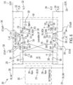
- the level-shifter LPF circuit 601 of FIG. 6 includes the switches 310, 312, 314, 316, 318, 320, 322, 324 and C2 328, 332 of FIG. 3 .
- the level-shifter LPF circuit 601 of this example splits C1 326, 330 of FIG. 3 into at least two capacitors, C1a 602, 606 and C1b 604, 608 which is described below.
- a parasitic capacitance 610 (identified by Cpar) may exist in connection with a second plate of C1 326 (e.g., the plate of C1 326 coupled to SW2 312 and SW4 316, the plate of C1 330 coupled to SW6 320 and SW8 324).
- the parasitic capacitance 610 may introduce input signal attenuation and degrade signal quality of the differential signal.
- C1/(C1+Cpar) is an attenuation factor that may cause a mismatch between high-frequency and low-frequency components of the differential signal.
- the level-shifter LPF circuit 601 of the illustrated example can be configured to utilize a differential sampling technique on the input signals 208, 210.
- the differential sampling technique and the splitting of C 1 326 of FIG. 3 into multiple capacitors as illustrated in FIG. 6 can overcome the effects of the parasitic capacitance 610.
- the differential sampling technique can enable the selection of the splitting ratio of C1 such that the parasitic capacitance may be canceled out and/or otherwise reduced to maintain a relatively flat frequency response.
- a flat response may correspond to a low-frequency gain matching and/or otherwise closely tracking a high-frequency gain.
- the differential sampling technique can be implemented by coupling RX_INP 208 to SW3 314 and SW5 318 and by coupling RX_INN 210 to SW1 310 and SW7 322.
- C1 326 of FIG. 3 is split into C1a 602 and C1b 604 and C1 330 is split into C1a 606 and C1b 608.
- C1a 602 and C1a 606 have the same capacitance while in other embodiments they may have different capacitances.
- C1b 604 and C1b 608 have the same capacitance while in other embodiments they may have different capacitances.
- the selection of a ratio of C1a/C1b can control (e.g., precisely control) the DC-coupling path gain (e.g., the DC-coupling path gain of (Vx_P-Vx_N) / (RX_INP-RX_INN)) as illustrated in the example of Equation (8) below:
- Vx _ P ⁇ Vx _ N 2 ⁇ RX _ INP ⁇ RX _ INN ⁇ C 1 a C 1 a + C 1 b + Cpar ,
- the splitting of C1326 into C1a 602 and C1b 604 (and the splitting of C1 330 into C1a 606 and C1b 608) provides gain control that may be tuned to cancel out the attenuation factor arising from Cpar 610.
- FIG. 7 is a timing diagram 700 that depicts waveforms 702, 704, 706, 708, 710, 712 associated with the level-shifter LPF circuit 601 of FIG. 6 .
- the waveforms 702, 704, 706, 708, 710, 712 may illustrate nodes VCloutP 340 and VCloutN 344 of FIG. 6 charging nodes Vx_P 232 and Vx_N 234 of FIGS. 2 and/or 6 to the differential input (e.g., RXINP-RXINN) with a desired output common mode (e.g., RX_INCM 236) in two exemplary cycles (e.g., two exemplary clock cycles).
- a first waveform 702 may represent PHI1 334 of FIGS. 3 and/or 6 with respect to time and a second waveform 704 may represent PHI2 336 of FIGS. 3 and/or 6 with respect to time.
- a third waveform 706 is depicted and may represent a voltage at node VClinP 338 of FIGS. 3 and/or 6 with respect to time.
- a fourth waveform 708 is depicted and may represent a voltage at node VClinN 342 of FIGS. 3 and/or 6 with respect to time.
- a fifth waveform 710 is shown and may represent a voltage at node VCloutP 340 of FIGS. 3 and/or 6 with respect to time.
- a sixth waveform 712 is shown and may represent a voltage at node VCloutN 344 of FIGS. 3 and/or 6 with respect to time. Further depicted are voltage levels corresponding to RX_INP 208, RX_INN 210, and RX_INCM 236 of FIGS. 2 , 3 , and/or 6.
- PHI1 334 has a falling edge and PHI2 336 has a rising edge.
- SW1 310, SW2 312, SW5 318, and SW6 320 of FIGS. 3 and/or 6 may open at the first time 714 and SW3 314, SW4 316, SW7 322, and SW8 324 of FIGS. 3 and/or 6 may close at the first time 714.
- the voltage at node VClinP 338 increases from RX_INN 210 and approaches the voltage of RX_INP 208, which contrasts the timing diagram 500 of FIG. 5 .
- the voltage at node VClinP 338 increases from CM_IN 212 at the first time 514.
- the utilization of differential sampling as shown in FIG. 6 causes the voltage at VClinP 338 to charge to the input opposite polarity, such as by alternating between RX_INP 208 and RX_INN 210.
- the voltage at node VCloutP 340 increases from RX_INCM 236 to a first voltage level 716 and voltage at the first voltage level 716 is output at node Vx_P 232 of FIGS. 2 and/or 6.
- the voltage at node VClinN 342 decreases from RX_INP 208 and approaches the voltage of RX_INN 210, which contrasts the timing diagram 500 of FIG. 5 .
- the voltage at node VClinN 342 decreases from CM_IN 212 at the first time 514.
- the utilization of differential sampling as shown in FIG. 6 causes the voltage at VClinN 342 to alternate between RX_INN 210 and RX_INP 208.
- the voltage at node VCloutN 344 decreases from RX_INCM 236 to a second voltage level 718 and voltage at the second voltage level 718 is output at node Vx_N 234.
- the difference between the voltages at nodes VClinP 338 and VClinN 342 reaches the voltage of the differential signal (RXINP-RXINN).
- PHI1 334 has a rising edge and PHI2 336 has a falling edge.
- SW1 310, SW2 312, SW5 318, and SW6 320 may close at the third time 722 and SW3 314, SW4 316, SW7 322, and SW8 324 may open at the third time 722.
- the voltage at node VClinP 338 decreases from RX_INP 208 and approaches RX_INN 210, which contrasts the timing diagram 500 of FIG. 5 .
- the voltage at node VClinP 338 decreases from RX_INP 208 and approaches CM_IN 212 at the first time 514.
- the voltage at node VCloutP 340 decreases towards RX_INCM 236 and the voltage at the node Vx_P 232 is maintained at the first voltage level 716.
- the voltage at node VClinN 342 increases from RX_INN 210 and approaches RX_INP 208, which contrasts the timing diagram 500 of FIG. 5 .
- the voltage at node VClinN 342 increases from RX_INN 210 and approaches CM_IN 212 at the third time 522.
- the voltage at node VCloutN 344 increases towards RX_INCM 236 and the voltage at the node Vx_N 234 is maintained at the second voltage level 718.
- PHI 1334 has a falling edge and PHI2 336 has a rising edge.
- SW1 310, SW2 312, SW5 318, and SW6 320 may open at the fourth time 724 and SW3 314, SW4 316, SW7 322, and SW8 324 may close at the fourth time 724.
- the voltage at node VClinP 338 increases from RX_INN 210 and approaches the voltage of RX_INP 208, which contrasts the timing diagram 500 of FIG. 5 .
- the voltage at node VClinP 338 increases from CM_IN 212 at the fourth time 524.
- the voltage at node VCloutP 340 increases from the first voltage level 716 to a third voltage level 726 and a voltage at the third voltage level 726 is output as the voltage at node Vx_P 232.
- the voltage at node VClinN 342 decreases from RX_INP 208 and approaches the voltage of RX_INN 210, which contrasts the timing diagram 500 of FIG. 5 .
- the voltage at node VClinN 342 decreases from CM_IN 212 at the fourth time 724.
- the voltage at node VCloutN 344 decreases from the second voltage level 718 to a fourth voltage level 728 and a voltage at the fourth voltage level 728 is output as the voltage at node Vx_N 234.
- the difference between the voltages at nodes VClinP 338 and VClinN 342 reaches the voltage of the differential signal (RXINP-RXINN).
- the difference between the voltages at nodes VCloutP 340 and VCloutN 344 reaches the voltage of 2*(RXINP-RXINN) and is output as the voltage between nodes Vx_P 232 and Vx_N 234.
- the nodes VClinP 338 and VClinN 342 can transfer twice the voltage input step to the nodes of VCloutP 340 and VCloutN 344.
- the nodes VCloutP 340 and VCloutN 344 charge the nodes Vx_P 232 and Vx_N 234 to 2*(RXINP-RXINN) with a desired output common mode represented by RX_INCM 236 in two cycles.
- the number of clock cycles to charge the Vx_P 232 and Vx_N 234 nodes to the differential input (RXINP-RXINN) can be based on the ratio of the capacitances of C1a 602, 606 and C1b 604, 608 and C2 328 of FIG. 6 .
- PHI1 334 has a rising edge and PHI2 336 has a falling edge.
- SW1 310, SW2 312, SW5 318, and SW6 320 may close at the sixth time 732 and SW3 314, SW4 316, SW7 322, and SW8 324 may open at the sixth time 732.
- the voltage at node VClinP 338 decreases from RX_INP 208 and approaches RX_INN 210, which contrasts the timing diagram 500 of FIG. 5 .
- the voltage at node VClinP 338 decreases from RX_INP 208 and approaches CM_IN 212 at the sixth time 532.
- the voltage at node VCloutP 340 decreases towards RX_INCM 236 and the voltage at the node Vx_P 232 is maintained at the third voltage level 726.
- the voltage at node VClinN 342 increases from RX_INN 210 and approaches RX_INP 208, which contrasts the timing diagram 500 of FIG. 5 .
- the voltage at node VClinN 342 increases from RX_INN 210 and approaches CM_IN 212 at the sixth time 532.
- the voltage at node VCloutN 344 increases towards RX_INCM 236 and the voltage at the node Vx_N 234 is maintained at the fourth voltage level 728.
- FIG. 8 is a schematic illustration of another example implementation of the AC coupling circuit 200 of FIG. 2 .
- the AC coupling circuit 200 depicted in FIG. 8 includes the anti-aliasing low-pass filter 301 of FIG. 3 and yet another example implementation of a level-shifter LPF circuit 802.
- the level-shifter LPF circuit 802 can implement the switched-capacitor signal-processing circuit 240 of FIG. 2 .
- the level-shifter LPF circuit 802 of FIG. 8 includes the switches 310, 312, 314, 316, 318, 320, 322, 324 and C2 328, 332 of FIG. 3 .
- the level-shifter LPF circuit 802 includes C1a 602, 606 and C1b 604, 608 of FIG. 6 .
- the level-shifter LPF circuit 802 implements the differential sampling technique shown in FIG. 6 .
- the level-shifter LPF circuit 802 can be configured to implement positive-charge pumps.
- the level-shifter LPF circuit 802 can be configured to include C1b 604, 608 as a positive-charge pump such that the common mode of OUTP/N 218, 220 can achieve voltages greater than a supply voltage.
- C1b 604 is coupled to a ninth switch 804 (identified by SW9) and a tenth switch 806 (identified by SW10) to implement a positive-charge pump.
- C1b 608 is coupled to an eleventh switch 808 (identified by SW11) and a twelfth switch 810 (identified by SW12) to implement another positive charge-pump.
- SW9 804, SW10 806, SW11 808, and SW12 810 are implemented by transistors.
- SW9 804 and SW11 808 are controlled by PHI1 334 and SW10 806 and SW12 810 are controlled by PHI2 336.
- the positive charge pumps can result in the output common mode, which may be represented by the common mode of OUTP 218 and OUTN 220, to reach voltages greater than a supply voltage 812 (identified by VDD).
- VDD supply voltage 812
- SW9 804 is closed and SW10 806 is open, which causes a reference voltage 814 (identified by VSS), which is less than VDD 812, to be applied to C1b 604, 608.
- VSS reference voltage
- the voltage across C1b 604, 608 may be represented by RX_INCM 236 because RX_INCM 236 is applied to first ones of the plates of C1b 604, 608 and VSS 814 is applied to second ones of the plates of C1b 604, 608, opposite the first ones.
- SW9 804 is open and SW10 806 is closed, which causes VDD 812 to be applied to C1b 604, 608.
- the positive-charge pumps add a voltage corresponding to the term "VDD*C1b/(C1a+C1b+Cpar)" of Equation (9) above to RX_INCM 236 to thereby reach a voltage greater than VDD 812.
- a lower voltage architecture (e.g., a lower swing voltage architecture) may be used for generation of RX_INCM 236 and the level-shifter LPF circuit 802 may reach at least VDD 812 because the output common mode can result in voltages greater than VDD 812.
- a lower (e.g., a negative) DC common mode may be implemented if C1b 604, 608 are configured as negative-charge pumps.
- FIG. 9 is a schematic illustration of another example implementation of the AC coupling circuit 110 of FIG. 1 and/or the AC coupling circuit 200 of FIG. 2 .
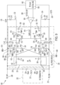
- FIG. 9 depicts an AC coupling circuit 900 that includes the anti-aliasing low-pass filter 301 of FIG. 3 , the level-shifter LPF circuit 802 of FIG. 8 , a receiver (RX) circuit 902, and a comparator 904.
- the RX circuit 902 is a circuit that receives the output signals 218, 220 and decodes (e.g., translates) them into a form that can drive additional circuitry.
- the RX circuit 902 may be an Ethernet receiver circuit that translates the output signals 218, 220 into digital zeros or ones, which may be output to a computer-hardware processor.
- the AC coupling circuit 900 can be configured to implement and/or perform discrete-time common-mode feedback.
- the AC coupling circuit 900 can implement a common-mode feedback loop, which includes at least the RX circuit 902 and the comparator 904, to operate as a first-order Sigma-Delta modulator.
- the RX circuit 902 can receive the output signals 218, 220 and sense (e.g., determine) an output common mode based on the output signals 218, 220.
- the RX circuit 902 can generate a sense signal 906 (identified by OUTCM_SNS) based on the output common mode.
- the sense signal 906 can represent the sensed output common mode voltage of the RX circuit 902.
- the RX circuit 902 can output OUTCM_SNS 906 to a first input (identified by a negative sign of the comparator 904 in FIG. 9 ) (e.g., a first comparator input) of the comparator 904.
- the comparator 904 can compare OUTCM_SNS 906 to a reference signal 908 (identified by OUTCM_REF) at a second input (identified by a positive sign of the comparator 904 in FIG. 9 ) (e.g., a second comparator input) of the comparator 904.
- OUTCM_REF 908 is an output common mode reference signal, which can represent a desired (e.g., an ideal) output common mode of the RX circuit 902.
- OUTCM_REF 908 can represent a target output common mode voltage for operation of the RX circuit 902.
- the comparator 904 is a clocked comparator. In some embodiments, the comparator 904 is clocked at SC_freq. For example, the comparator 904 can be clocked at a clock input of the comparator 904 using PHI1 334, which may change signal magnitudes at a frequency of SC_freq. In example operation, during PHI1 334, the comparator 904 can compare OUTCM_SNS 906 and OUTCM_REF 908 and output a feedback signal 910 (identified by CMFB_OUT) to the level-shifter LPF circuit 802. In this example, CMFB_OUT 910 is a common mode feedback output signal, which can indicate whether OUTCM_SNS 906 is greater than or less than a target output common mode of the RX circuit 902.
- the comparator 904 can feedback a logic level of VDD 812 or VSS 814 at CMFB_OUT 910. For example, the comparator 904 can output a logic level of VDD 812 from a comparator output of the comparator 904 in response to a determination that OUTCM_REF 908 is greater than OUTCM_SNS 906. In some embodiments, the comparator 904 can output a logic level of VSS 814 in response to a determination that OUTCM_REF 908 is less than OUTCM_SNS 906.
- the rail-to-rail CMFB_OUT 910 logic level transitions can be filtered by the bandwidths of the filters implemented by the level-shifter LPF circuit 802 and/or the AC coupling filter (e.g., the filter implemented by C_AC 214 and R_AC 222, the filter implemented by C_AC 216 and R_AC 224).
- the AC coupling filter e.g., the filter implemented by C_AC 214 and R_AC 222, the filter implemented by C_AC 216 and R_AC 224.
- FIG. 10 is a timing diagram 1000 that depicts example waveforms 1002, 1004, 1006, 1008, 1010 associated with the AC coupling circuit 900 of FIG. 9 .
- the waveforms 1002, 1004, 1006, 1008, 1010 can represent transient waveforms depicting the settling behavior of the common-mode feedback loop of FIG. 9 operating as a first-order Sigma-Delta modulator.
- a first waveform 1002 is depicted and can represent OUTCM_SNS 906 of FIG. 9 with respect to time.
- a second waveform 1004 is depicted and can represent OUTCM_REF 908 of FIG. 9 with respect to time.
- a third waveform 1006 is depicted and can represent CMFB_OUT 910 of FIG. 9 with respect to time.
- a fourth waveform 1008 is depicted and can represent a common mode of the Vx nodes of FIG. 9 (identified by Vx_CM 1012).
- VX_CM 1012 can represent a voltage determined by half of the sum ofVx_P 232 and Vx_N 234.
- a fifth waveform 1010 is depicted and can represent an output common mode of the RX circuit 902 of FIG. 9 (identified by OUT_CM 1014).
- OUT_CM 1014 can represent a voltage determined by half of the sum of OUTP 218 and OUTN 220.
- the comparator 904 of FIG. 9 can compare OUTCM_SNS 906 and OUTCM_REF 908 and output CMFB_OUT 910 based on the comparison.
- CMFB_OUT 910 can be updated to VDD 1016 or VSS 1018 every cycle based on the comparison.
- CMFB_OUT 910 is updated to VDD 1016 after a determination that OUTCM_REF 908 is greater than OUTCM_SNS 906.
- CMFB_OUT 910 is updated to VSS 1018 after a determination that OUTCM_REF 908 is less than OUTCM_SNS 906.
- the settling behavior of Vx_CM 1012 can be the result of the filters implemented by the ratio of C1a 602 and C1b 604 and C2 328 (or the ratio of C1a 606 and C1b 608 and C2 332).
- Vx_CM 1012 can settle to approximately OUT_CM 1014 over time.
- further filtering is achieved at the output nodes (OUTP 218 and OUTN 220) because of the AC coupling circuit cut-off frequency (e.g., f_AC implemented by C_AC 214 and R_AC 222, f_AC implemented by C_AC 216 and R_AC 224).
- FIG. 11 is a schematic illustration of another example implementation of the AC coupling circuit 110 of FIG. 1 and/or the AC coupling circuit 200 of FIG. 2 .
- FIG. 11 depicts an AC coupling circuit 1100 that includes the anti-aliasing low-pass filter 301 of FIG. 3 , the level-shifter LPF circuit 802 of FIG. 8 , the RX circuit 902 and the comparator 904 of FIG. 9 , a thirteenth switch 1102 (identified by SW13), a fourteenth switch 1104 (identified by SW14), a fifteenth switch 1106 (identified by SW15), a sixteenth switch 1108 (identified by SW16), an inverter 1110, and a multiplexer 1112.
- SW13 1102, SW14 1104, SW15 1106, and/or SW16 1108 can be implemented by transistors.
- SW13 1102 and SW14 1104 have non-inverting inputs (e.g., non-inverting terminals) and SW15 1106 and SW16 1108 have inverting inputs (e.g., inverting terminals).
- the comparator 904 can be relatively low powered because noise that may be introduced in the AC coupling circuit 1100 by the comparator 904 is heavily filtered by f_SC and f_AC.
- the comparator 904 can have an offset that may introduce an offset in the common mode feedback loop.
- the AC coupling circuit 1100 of the illustrated example can be configured to overcome and/or correct the offset in the common mode feedback loop that may be introduced by the comparator 904. For example, an offset mitigation technique such as chopping may be utilized.
- the AC coupling circuit 1100 can be configured to use chopping by swapping inputs to the comparator 904 every cycle.
- a chop (or chopping) clock 1114 (identified by CLK_CHOP) can control SW13 1102, SW14 1104, SW15 1106, and SW16 1108.
- SW13 1102 and SW14 1104 can close and SW15 1106 and SW16 1108 can open.
- OUTCM_REF 908 can be provided to the positive input of the comparator 904 and OUTCM_SNS 906 can be provided to the negative input of the comparator 904.
- SW13 1102 and SW14 1104 can open and SW15 1106 and SW16 1108 can close.
- OUTCM_REF 908 can be provided to the negative input of the comparator 904 and OUTCM_SNS 906 can be provided to the positive input of the comparator 904.
- the output of the comparator 904 can be inverted to maintain comparator polarity.
- the output of the comparator 904 is provided to a first input (e.g., a first multiplexer input) of the multiplexer 1112 and an inverter input of the inverter 1110.
- An inverter output of the inverter 1110 is coupled to a second input (e.g., a second multiplexer input) of the multiplexer 1112.
- the multiplexer 1112 is clocked at a clock input of the multiplexer 1112 to CLK_CHOP 1114 such that the multiplexer 1112 alternates between outputting the first input or the second input as CMFB_OUT 910.
- an output (e.g., a multiplexer output) of the multiplexer 1112 can output either the first input or the second input every clock cycle to correspond to a polarity associated with the comparator 904.
- the offset that may be introduced by the comparator 904 is modulated and/or removed by CLK_CHOP 1114 and filtered by f_SC and f_AC.
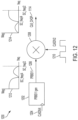
- FIG. 12 is a schematic illustration of an example implementation of a clock circuit 1200 to perform a chopping modulation technique.
- the clock circuit 1200 can generate CLK_CHOP 1114 of FIG. 11 .
- the clock circuit 1200 of the illustrated example is implemented at least in part by a pseudorandom binary sequence (PRBS) generator 1202.
- PRBS generator 1202 may be implemented by one or more analog circuits, one or more digital circuits, and/or one or more ICs, such as being implemented by PRBS generation circuitry.
- the PRBS generator 1202 of this example receives a first divided clock signal 1204 (identified by CLKDIV4) and generates a PRBS signal 1206 (identified by PRBS 11) based on the first divided clock signal 1204.
- the PRBS generator 1202 of this example is an 11-bit PRBS generator that is configured to generate the PRBS signal 1206 as an 11-bit PRBS pattern at a quarter rate of SC_freq.
- the quarter rate of SC_freq can be achieved by dividing SC_freq by 4 to yield CLKDIV4 1204.
- the PRBS generator 1202 may be configured to generate the PRBS signal 1206 using any other pattern and/or at any other rate.
- the PRBS generator 1202 outputs the PRBS signal 1206 to a multiplier 1208 to multiply the PRBS signal 1206 and a second clock signal 1210 to generate CLK_CHOP 1114.
- the multiplier 1208 can be configured such that the PRBS signal 1206 is up-modulated by a "1,+1" clock pattern at SC_freq/2 to output CLK_CHOP 1114.
- the multiplier 1208 may be implemented by one or more analog circuits, one or more digital circuits, and/or one or more ICs, such as being implemented by multiplication circuitry (e.g., voltage multiplication circuitry).
- the clock circuit 1200 can perform the chopping modulation technique to spread portion(s) of the offset power between the frequencies of SC_freq/4 and SC_freq/2, which can be filtered by the f_SC and f_AC filters as described herein.
- PRBS 11 1206 may have an associated frequency response 1212 as shown in FIG. 12 , which plots the magnitude of PRBS11 1206 as a function of frequency.
- the offset power is greater in the frequency range of 0 to SC_freq/4 than in the frequency range of SC_freq/4 to SC_freq/2.
- CLK_CHOP 1114 may have an associated frequency response 1214 as shown in FIG.
- the chopping modulation technique can spread the offset power between the frequencies SC_freq/4 to SC_freq/2 to facilitate their filtering by the f_SC and f_AC filters.
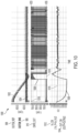
- FIG. 13 is a plot 1300 that depicts a waveform 1302 representing a power spectral density (PSD) of CLK_CHOP 1114 of FIGS. 11 and/or 12 with respect to frequency measured in hertz (Hz).
- PSD power spectral density
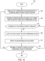
- FIG. 14 is a flowchart 1400 of an example method to output a differential signal to a receiver input stage of a receiver.
- the flowchart 1400 begins at block 1402, at which a receiver system, such as the receiver system 100 of FIG. 1 , can sense an output common mode voltage associated with a differential signal of an input stage of a receiver.
- a receiver system such as the receiver system 100 of FIG. 1
- the RX circuit 902 of FIGS. 9 and/or 11 can sense the output common mode voltage and output the sensed voltage as OUTCM_SNS 906.
- the receiver system can determine a difference between the sensed output common mode voltage and a target output common mode voltage. For example, the comparator 904 of FIGS. 9 and/or 11 can determine whether OUTCM_REF 908 is greater than or less than OUTCM_SNS 906 based on the difference thereof.
- the receiver system can determine whether the difference satisfies a threshold.
- the comparator 904 can determine that the difference between OUTCM_REF 908 and OUTCM_SNS 906 is a positive voltage and thereby satisfies a comparison threshold of the comparator 904 to output CMFB_OUT 910 as VDD 812.
- the comparator 904 can determine that the difference between OUTCM_REF 908 and OUTCM_SNS 906 is a negative voltage and thereby does not satisfy the comparison threshold of the comparator 904 to output CMFB_OUT 910 as VSS 814.
- the receiver system determines that the difference does not satisfy the threshold, control proceeds to block 1412. Otherwise, control proceeds to block 1408.
- the receiver system outputs a voltage to adjust the output common mode voltage.
- the comparator 904 can output CMFB_OUT 910 as VDD 812 to be injected into Vx_P 232 and Vx_N 234 and adjust Vx_CM 1012 of FIG. 12 by increasing Vx_CM 1012.
- OUT_CM 1014 can be adjusted (e.g., increased) to ensure proper operation of the RX circuit 902.
- the receiver system can operate the receiver based on the adjustment.
- the RX circuit 902 can be operated (e.g., continue to be operated) using the adjusted output common mode voltage.
- the receiver system can determine whether to continue to control the output common mode voltage of the receiver. For example, the receiver system may continue to control the output common mode voltage of the receiver while the receiver system is powered and/or enabled. If, at block 1412, the receiver system determines to continue to control the output common mode voltage of the receiver, control returns to block 1402. Otherwise, the method represented by the flowchart 1400 of FIG. 14 concludes.
- the phrase "at least one,” in reference to a list of one or more elements, should be understood to mean at least one element selected from any one or more of the elements in the list of elements, but not necessarily including at least one of each and every element specifically listed within the list of elements and not excluding any combinations of elements in the list of elements.
- This definition also allows that elements may optionally be present other than the elements specifically identified within the list of elements to which the phrase "at least one" refers, whether related or unrelated to those elements specifically identified.
- a reference to "A and/or B", when used in conjunction with open-ended language such as “comprising” can refer, in one embodiment, to A only (optionally including elements other than B); in another embodiment, to B only (optionally including elements other than A); in yet another embodiment, to both A and B (optionally including other elements); etc.
Landscapes
- Engineering & Computer Science (AREA)
- Power Engineering (AREA)
- Microelectronics & Electronic Packaging (AREA)
- Computer Networks & Wireless Communication (AREA)
- Signal Processing (AREA)
- Dc Digital Transmission (AREA)
- Amplifiers (AREA)
Applications Claiming Priority (2)
| Application Number | Priority Date | Filing Date | Title |
|---|---|---|---|
| US202263381939P | 2022-11-02 | 2022-11-02 | |
| US18/477,538 US20240146269A1 (en) | 2022-11-02 | 2023-09-28 | Differential all-pass coupling circuit with common mode feedback |
Publications (2)
| Publication Number | Publication Date |
|---|---|
| EP4366163A2 true EP4366163A2 (de) | 2024-05-08 |
| EP4366163A3 EP4366163A3 (de) | 2024-10-09 |
Family
ID=88647715
Family Applications (1)
| Application Number | Title | Priority Date | Filing Date |
|---|---|---|---|
| EP23207140.7A Pending EP4366163A3 (de) | 2022-11-02 | 2023-10-31 | Differentielle allpass-koppelschaltung mit gleichtaktrückkopplung |
Country Status (2)
| Country | Link |
|---|---|
| US (1) | US20240146269A1 (de) |
| EP (1) | EP4366163A3 (de) |
Families Citing this family (1)
| Publication number | Priority date | Publication date | Assignee | Title |
|---|---|---|---|---|
| TWI864974B (zh) * | 2023-08-18 | 2024-12-01 | 瑞昱半導體股份有限公司 | 具有直流位準位移的有線通訊接收器 |
Family Cites Families (4)
| Publication number | Priority date | Publication date | Assignee | Title |
|---|---|---|---|---|
| EP1257053A1 (de) * | 2001-05-11 | 2002-11-13 | Telefonaktiebolaget L M Ericsson (Publ) | Differenzsignalübertragungsschaltung |
| US7386290B2 (en) * | 2004-07-30 | 2008-06-10 | Broadcom Corporation | RX dual-band mixer |
| US8638165B2 (en) * | 2011-06-06 | 2014-01-28 | Qualcomm Incorporated | Switched-capacitor DC blocking amplifier |
| US10944599B2 (en) * | 2019-06-28 | 2021-03-09 | Adtran, Inc. | Systems and methods for communicating high speed signals in a communication device |
-
2023
- 2023-09-28 US US18/477,538 patent/US20240146269A1/en active Pending
- 2023-10-31 EP EP23207140.7A patent/EP4366163A3/de active Pending
Also Published As
| Publication number | Publication date |
|---|---|
| EP4366163A3 (de) | 2024-10-09 |
| US20240146269A1 (en) | 2024-05-02 |
Similar Documents
| Publication | Publication Date | Title |
|---|---|---|
| CN100581146C (zh) | 差分信号接收设备和差分信号传输系统 | |
| CN112042117B (zh) | 具有多个独立输出级的d类放大器 | |
| US20130214865A1 (en) | Capacitive level-shifting circuits and methods for adding dc offsets to output of current-integrating amplifier | |
| TWI740539B (zh) | 藉助於差動漂移電流感測來進行基線漂移修正的裝置 | |
| US20200210008A1 (en) | Touch Sensing Device And Display Apparatus Including The Same | |
| US7961050B1 (en) | Integrated circuits including an equalizer and operating methods thereof | |
| EP4366163A2 (de) | Differentielle allpass-koppelschaltung mit gleichtaktrückkopplung | |
| US20170229961A1 (en) | Current balance method for multiphase switching regulators | |
| CN110739924B (zh) | 用来进行基线漂移修正的装置 | |
| CN108572276A (zh) | 差分驱动的无线谐振发射器的峰值电压检测 | |
| EP3286833A1 (de) | Verfahren und vorrichtung zum mischen von signalen unter verwendung einer ladungsunterdrückungsschaltung | |
| US10476489B2 (en) | Signal transmission circuit | |
| US8803595B2 (en) | Common mode noise cancellation circuit for unbalanced signals | |
| CN103973231A (zh) | 放大电路的电压调整电路及相关的调整方法 | |
| JP6381960B2 (ja) | オーディオアンプ、オーディオ出力回路、オーディオ用集積回路、電子機器、オーディオ信号の増幅方法 | |
| CN115914939A (zh) | 用于生成调制协议以输出音频的方法和装置 | |
| CN117997362A (zh) | 具有共模反馈的差分全通耦合电路 | |
| KR19980018571A (ko) | 전자 회로 및 저항기 네트워크 | |
| KR102946789B1 (ko) | Vco(voltage controlled oscillator) 또는 다른 애플리케이션들을 위한 버퍼 | |
| US8400183B1 (en) | Voltage conversion | |
| US20160181997A1 (en) | Signal amplifying circuit | |
| US11824530B2 (en) | Low latency, broadband power-domain offset-correction signal level circuit implementation | |
| US11722816B2 (en) | Signal processing circuit | |
| JPS6378612A (ja) | レベルシフト回路 | |
| US9459648B2 (en) | AC coupled single-ended LVDS receiving circuit comprising low-pass filter and voltage regulator |
Legal Events
| Date | Code | Title | Description |
|---|---|---|---|
| PUAI | Public reference made under article 153(3) epc to a published international application that has entered the european phase |
Free format text: ORIGINAL CODE: 0009012 |
|
| STAA | Information on the status of an ep patent application or granted ep patent |
Free format text: STATUS: THE APPLICATION HAS BEEN PUBLISHED |
|
| AK | Designated contracting states |
Kind code of ref document: A2 Designated state(s): AL AT BE BG CH CY CZ DE DK EE ES FI FR GB GR HR HU IE IS IT LI LT LU LV MC ME MK MT NL NO PL PT RO RS SE SI SK SM TR |
|
| PUAL | Search report despatched |
Free format text: ORIGINAL CODE: 0009013 |
|
| AK | Designated contracting states |
Kind code of ref document: A3 Designated state(s): AL AT BE BG CH CY CZ DE DK EE ES FI FR GB GR HR HU IE IS IT LI LT LU LV MC ME MK MT NL NO PL PT RO RS SE SI SK SM TR |
|
| RIC1 | Information provided on ipc code assigned before grant |
Ipc: H03F 3/45 20060101ALI20240904BHEP Ipc: H03F 3/195 20060101AFI20240904BHEP |
|
| STAA | Information on the status of an ep patent application or granted ep patent |
Free format text: STATUS: REQUEST FOR EXAMINATION WAS MADE |
|
| 17P | Request for examination filed |
Effective date: 20250409 |
|
| RAP3 | Party data changed (applicant data changed or rights of an application transferred) |
Owner name: MEDIATEK INC. |