EP4358354A1 - Electronic device and an operating method of the electronic device - Google Patents
Electronic device and an operating method of the electronic device Download PDFInfo
- Publication number
- EP4358354A1 EP4358354A1 EP23191701.4A EP23191701A EP4358354A1 EP 4358354 A1 EP4358354 A1 EP 4358354A1 EP 23191701 A EP23191701 A EP 23191701A EP 4358354 A1 EP4358354 A1 EP 4358354A1
- Authority
- EP
- European Patent Office
- Prior art keywords
- voltage
- corruption
- connector
- terminal
- electronic device
- Prior art date
- Legal status (The legal status is an assumption and is not a legal conclusion. Google has not performed a legal analysis and makes no representation as to the accuracy of the status listed.)
- Pending
Links
- 238000011017 operating method Methods 0.000 title description 7
- 238000001514 detection method Methods 0.000 claims abstract description 156
- 238000012546 transfer Methods 0.000 claims abstract description 16
- 238000000034 method Methods 0.000 claims description 13
- 238000010586 diagram Methods 0.000 description 25
- 239000000356 contaminant Substances 0.000 description 12
- 230000004044 response Effects 0.000 description 12
- 230000003213 activating effect Effects 0.000 description 8
- 101150088150 VTH2 gene Proteins 0.000 description 5
- 230000008569 process Effects 0.000 description 5
- 101100102849 Saccharomyces cerevisiae (strain ATCC 204508 / S288c) VTH1 gene Proteins 0.000 description 4
- 238000006243 chemical reaction Methods 0.000 description 4
- 230000003071 parasitic effect Effects 0.000 description 4
- 230000004913 activation Effects 0.000 description 3
- 238000005260 corrosion Methods 0.000 description 3
- 230000007797 corrosion Effects 0.000 description 3
- 230000009849 deactivation Effects 0.000 description 3
- 230000000903 blocking effect Effects 0.000 description 2
- 238000012544 monitoring process Methods 0.000 description 2
- 102100027367 Cysteine-rich secretory protein 3 Human genes 0.000 description 1
- 102100040615 Homeobox protein MSX-2 Human genes 0.000 description 1
- 101000726258 Homo sapiens Cysteine-rich secretory protein 3 Proteins 0.000 description 1
- 101000967222 Homo sapiens Homeobox protein MSX-2 Proteins 0.000 description 1
- 101000773184 Homo sapiens Twist-related protein 1 Proteins 0.000 description 1
- 102100030398 Twist-related protein 1 Human genes 0.000 description 1
- 208000015842 craniosynostosis 2 Diseases 0.000 description 1
- 238000012423 maintenance Methods 0.000 description 1
- 238000012986 modification Methods 0.000 description 1
- 230000004048 modification Effects 0.000 description 1
- 239000004065 semiconductor Substances 0.000 description 1
- 210000004243 sweat Anatomy 0.000 description 1
- XLYOFNOQVPJJNP-UHFFFAOYSA-N water Substances O XLYOFNOQVPJJNP-UHFFFAOYSA-N 0.000 description 1
Images


Classifications
-
- H—ELECTRICITY
- H02—GENERATION; CONVERSION OR DISTRIBUTION OF ELECTRIC POWER
- H02J—CIRCUIT ARRANGEMENTS OR SYSTEMS FOR SUPPLYING OR DISTRIBUTING ELECTRIC POWER; SYSTEMS FOR STORING ELECTRIC ENERGY
- H02J7/00—Circuit arrangements for charging or depolarising batteries or for supplying loads from batteries
- H02J7/0029—Circuit arrangements for charging or depolarising batteries or for supplying loads from batteries with safety or protection devices or circuits
- H02J7/0036—Circuit arrangements for charging or depolarising batteries or for supplying loads from batteries with safety or protection devices or circuits using connection detecting circuits
-
- H—ELECTRICITY
- H02—GENERATION; CONVERSION OR DISTRIBUTION OF ELECTRIC POWER
- H02J—CIRCUIT ARRANGEMENTS OR SYSTEMS FOR SUPPLYING OR DISTRIBUTING ELECTRIC POWER; SYSTEMS FOR STORING ELECTRIC ENERGY
- H02J7/00—Circuit arrangements for charging or depolarising batteries or for supplying loads from batteries
- H02J7/0029—Circuit arrangements for charging or depolarising batteries or for supplying loads from batteries with safety or protection devices or circuits
- H02J7/00308—Overvoltage protection
-
- H—ELECTRICITY
- H02—GENERATION; CONVERSION OR DISTRIBUTION OF ELECTRIC POWER
- H02J—CIRCUIT ARRANGEMENTS OR SYSTEMS FOR SUPPLYING OR DISTRIBUTING ELECTRIC POWER; SYSTEMS FOR STORING ELECTRIC ENERGY
- H02J2207/00—Indexing scheme relating to details of circuit arrangements for charging or depolarising batteries or for supplying loads from batteries
- H02J2207/30—Charge provided using DC bus or data bus of a computer
Definitions
- Embodiments of the present disclosure described herein relate to an electronic device, and more particularly, to an electronic device for receiving a voltage from an external first device and transferring a voltage to an external second device and an operating method of the electronic device.
- a true wireless stereo (TWS) cradle functions as a station for wireless earphones.
- the TWS cradle may be supplied with a voltage from a first external device and may charge an internal battery.
- the TWS cradle may charge a second external device by transferring the voltage from the first external device or the charged voltage of the battery to the second external device.
- the TWS cradle may be equipped with a connector that is connected to the first external device.
- the connector may become contaminated by conductive contaminants such as water and sweat.
- the connector of the TWS cradle typically uses a receptacle, which has a structural characteristic that makes it challenging to detect and remove the contaminants.
- the voltage may be transferred through the contaminants, thereby leading to corrosion of both the connector of the TWS cradle and a connector of the first external device connected to the connector of the TWS cradle.
- Embodiments of the present disclosure provide an electronic device that can charge a second external device irrespective of whether a connector of the electronic device is contaminated or not. This is achieved by detecting corruption in the connector and blocking the electrical connection such that a voltage is not supplied from a first external device. Additionally, embodiments of the present disclosure provide an operating method of the electronic device.
- an electronic device including: a connector including a voltage terminal, a detection terminal, and a data terminal; a battery; a corruption detection circuit configured to detect whether the connector is corrupted; a voltage cutoff circuit connected with the voltage terminal of the connector, and configured to electrically connect the voltage terminal with an internal node when corruption of the connector is not detected by the corruption detection circuit and to electrically disconnect the voltage terminal from the internal node when the corruption is detected by the corruption detection circuit; a charging pin connected with the internal node, and configured to transfer a voltage of the internal node to an external device when the charging pin is connected with the external device, irrespective of whether the corruption is detected; and a power management integrated circuit connected between the internal node and the battery, and configured to charge the battery by using the voltage of the internal node or to generate the voltage of the internal node by using a voltage of the battery.
- an electronic device including: a connector including a voltage terminal, a detection terminal, and a data terminal; a battery; a corruption detection circuit configured to detect whether the connector is corrupted, using different techniques, according to whether an external voltage is supplied through the voltage terminal; a voltage cutoff circuit connected with the voltage terminal of the connector, and configured to electrically connect the voltage terminal with an internal node when corruption of the connector is not detected by the corruption detection circuit and to electrically disconnect the voltage terminal from the internal node when the corruption is detected by the corruption detection circuit; a power management integrated circuit configured to charge the battery by using a voltage of the internal node or to generate the voltage of the internal node by using a voltage of the battery; and a charging pin configured to transfer the voltage of the internal node to an external device when the charging pin is connected with the external device, wherein, when the external voltage is supplied through the voltage terminal and the corruption is not detected by the corruption detection circuit, the charging pin is configured to transfer the external voltage to the external device, and the power management integrated
- an operating method of an electronic device which is configured to be connected with a first external device through a connector and is configured to be connected with a second external device through a charging pin, the method including: detecting whether the connector is corrupted; blocking an electrical connection with a voltage terminal of the connector when the connector is corrupted; establishing the electrical connection with the voltage terminal of the connector when the connector is not corrupted; and providing a voltage to the second external device when the second external device is connected with the charging pin, irrespective of whether the connector is corrupted.
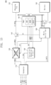
- FIG. 1 is a diagram illustrating an electronic device 100 according to an embodiment of the present disclosure.
- the electronic device 100 may be implemented with a true wireless stereo (TWS) cradle.
- the electronic device 100 may include a connector 110, a voltage cutoff circuit 120, a corruption detection circuit 130, a first switch 140, a charging pin 150, a power management integrated circuit (PMIC) 160, a second switch 170, a battery 180, and a micro control unit 190.
- TWS true wireless stereo
- PMIC power management integrated circuit
- the connector 110 may be connected with a first device (hereinafter referred to as a "first external device") located outside the electronic device 100.
- the connector 110 may be a receptacle or a USB Type-C receptacle.
- the connector 110 may include terminals for connecting with various lines of the first external device, which include voltage lines L_VBUS, ground lines L_GND, auxiliary lines L_SBU, and data lines L_DATA.
- the connector 110 may connect a voltage (e.g., VBUS) transferred through the voltage lines L_VBUS of the first external device with a first voltage line L1_VBUS in the electronic device 100.
- the connector 110 may transfer a ground voltage transferred through the ground lines L_GND of the first external device to a ground node of the electronic device 100.
- the connector 110 may connect signals transferred through the auxiliary lines L_SBU of the first external device with auxiliary voltage lines LI_SBU in the electronic device 100.
- the connector 110 may connect signals transferred through the data lines L_DATA of the first external device with data lines LI_DATA in the electronic device 100.
- the voltage cutoff circuit 120 may be connected between the first voltage line L1_VBUS and a second voltage line L2_VBUS.
- the voltage cutoff circuit 120 may operate in response to a first control signal CT1 received from the power management integrated circuit 160.
- the voltage cutoff circuit 120 may block or establish an electrical connection between the first voltage line L1_VBUS and the second voltage line L2_VBUS in response to the first control signal CT1.
- the voltage cutoff circuit 120 may detect whether an external voltage is supplied from the first external device to the first voltage line L1_VBUS through the connector 110. When the external voltage is supplied to the first voltage line L1_VBUS, the voltage cutoff circuit 120 may activate a detection signal VDET. For example, the detection signal VDET with a high level may be applied to the PMIC 160. When the external voltage is not supplied to the first voltage line L1_VBUS, the voltage cutoff circuit 120 may deactivate the detection signal VDET. For example, the detection signal VDET with a low level may be applied to the PMIC 160.
- the corruption detection circuit 130 may receive a second control signal CT2. In response to the second control signal CT2, the corruption detection circuit 130 may detect whether the connector 110 is corrupted. When the connector 110 is corrupted, the corruption detection circuit 130 may activate a corruption signal CRT. For example, the corruption signal CRT with a high level may be applied to the PMIC 160. When the connector 110 is not corrupted, the corruption detection circuit 130 may deactivate the corruption signal CRT. For example, the corruption signal CRT with a low level may be applied to the PMIC 160.
- the first switch 140 may operate in response to a first signal S1 received from the micro control unit 190. In response to the first signal S1, the first switch 140 may electrically connect the second voltage line L2_VBUS and a third voltage line L3_VBUS or may electrically disconnect the second voltage line L2_VBUS from the third voltage line L3_VBUS.
- the charging pin 150 may be configured to be connected with a second device (hereinafter referred to as a "second external device") located outside of the electronic device 100.
- the charging pin 150 may be connected with wireless earphones.
- the charging pin 150 may provide a voltage of the third voltage line L3_VBUS to the second external device to enable charging of the second external device.
- the charging pin 150 may include two or more charging pins.
- the power management integrated circuit 160 may receive the detection signal VDET from the voltage cutoff circuit 120.
- the power management integrated circuit 160 may step down the voltage of the third voltage line L3_VBUS, may charge the battery 180 with the stepped-down voltage, and may power the micro control unit 190.
- the power management integrated circuit 160 may step up the voltage of the third voltage line L3_VBUS and may supply the stepped-up voltage to the charging pin 150.
- each of the voltage cutoff circuit 120, the pin 150, and PMIC 160 are connected via an internal node, in this embodiment third voltage line L3_VBUS.
- the power management integrated circuit 160 may include a buck converter BUCK configured to step down a voltage and a boost converter BOOST configured to step up a voltage.
- the power management integrated circuit 160 may receive the detection signal VDET from the voltage cutoff circuit 120 through a general purpose input and output (GPIO) and may transfer the first control signal CT1 to the voltage cutoff circuit 120.
- GPIO general purpose input and output
- the power management integrated circuit 160 may control the voltage cutoff circuit 120 with the first control signal CT1 such that the first voltage line L1_VBUS and the second voltage line L2_VBUS are electrically disconnected.
- the power management integrated circuit 160 may control the voltage cutoff circuit 120 with the first control signal CT1 such that the first voltage line L1_VBUS and the second voltage line L2_VBUS are electrically connected.
- the second switch 170 may operate in response to a second signal S2 received from the micro control unit 190. In response to the second signal S2, the second switch 170 may electrically connect the power management integrated circuit 160 and the battery 180 or may electrically disconnect the power management integrated circuit 160 from the battery 180.
- the battery 180 may operate under control of the power management integrated circuit 160.
- the battery 180 may be charged by the voltage transferred from the power management integrated circuit 160.
- the battery 180 may output the charged voltage under control of the power management integrated circuit 160.
- the micro control unit 190 may control various operations of the electronic device 100.
- the micro control unit 190 may be reset when the detection signal VDET is activated.
- the micro control unit 190 may control the first switch 140 with the first signal S1.
- the micro control unit 190 may control the second switch 170 with the second signal S2.
- the first switch 140 or the second switch 170 which may be implemented as, for example, a transistor, may have a parasitic diode in a turn-off state.
- a leakage current may flow due to the parasitic diode.
- the connector 110 may be further corroded.
- the voltage cutoff circuit 120 may be designed to suppress the leakage current.
- the voltage cutoff circuit 120 may be implemented with an over voltage protection (OVP) circuit.
- the voltage cutoff circuit 120 may be manufactured with a separate integrated circuit.
- the electronic device 100 may transfer the external voltage to the second external device through the charging pin 150. Because DC-DC conversion such as step-up conversion and step-down conversion is not performed in the process of providing the voltage to the second external device, the electronic device 100 may charge the second external device with high efficiency.
- FIG. 2 illustrates an example of the connector 110.
- the connector 110 may be based on USB Type-C.
- Ground terminals T_GND may be connected to the ground lines L_GND of the first external device.
- Transmit terminals T_TX+ and T_TX-, second transmit terminals T_TX2+ and T_TX2-, receive terminals T_RX+ and T_RX-, and second receive terminals T_RX2+ and T_RX2- are connected with the data lines L_DATA of the first external device.
- Compatible terminals T_D+ and T_D- may support USB 2.0.
- the voltage terminals T_VBUS may be connected with the voltage lines L_VBUS of the first external device.
- Auxiliary terminals T_SBU1 and T_SBU2 may be connected with the auxiliary lines L_SBU of the first external device.
- Channel configuration terminals CC1 and CC2 may be used to configure a channel with the first external device.
- the use of the electronic device 100 is limited to basic functions such as a function of charging the second external device, for example, wireless earphones. Accordingly, the electronic device 100 may not communicate with the first external device through the auxiliary terminals T_SBU1 and T_SBU2. The electronic device 100 may use the auxiliary terminals T_SBU1 and T_SBU2 as detection terminals for detecting contaminants.
- FIG. 3 is a diagram illustrating an example of an operating method of the electronic device 100.
- the electronic device 100 may perform corruption management of the connector 110 through operation S11, operation S12, operation S13, and operation S14 and may perform charging management of the second external device through operation S21, operation S22, and operation S23 that are independent of or parallel to operation S11, operation S12, operation S13, and operation S14.
- the electronic device 100 may detect whether the connector 110 is corrupted.
- the electronic device 100 may periodically perform the detection.
- the power management integrated circuit 160 may detect that the connector 110 is corrupted by monitoring the activation of the corruption signal CRT.
- the power management integrated circuit 160 may detect that the connector 110 is not corrupted (e.g., the connector 110 is clean) by monitoring the deactivation (or maintenance of an inactive state) of the corruption signal CRT.
- the power management integrated circuit 160 may detect the corruption of the connector 110 when an activation pattern of the corruption signal CRT at different detection timings satisfies a given condition. After the corruption of the connector 110 is detected, if the corruption signal CRT remains deactivated or in the inactive state for two or more detection timings, the power management integrated circuit 160 may detect that the corruption of the connector 110 is resolved, indicating that the connector 110 is no longer corrupted.
- the electronic device 100 may block the electrical connection with the voltage terminal T_VBUS.
- the power management integrated circuit 160 may control the first control signal CT1 to activate the voltage cutoff circuit 120.
- the activated voltage cutoff circuit 120 may electrically disconnect the first voltage line L1_VBUS from the second voltage line L2_VBUS.
- the electronic device 100 may establish the electrical connection with the voltage terminal T_VBUS.
- the power management integrated circuit 160 may control the first control signal CT1 to deactivate the voltage cutoff circuit 120.
- the deactivated voltage cutoff circuit 120 may establish the electrical connection of the first voltage line L1_VBUS and the second voltage line L2_VBUS.
- the electronic device 100 may detect whether the second external device is connected with the charging pin 150. When it is detected in operation S22 that the second external device is connected with the charging pin 150, in operation S23, the electronic device 100 may provide the voltage to the second external device. For example, the charging pin 150 may provide the voltage of the third voltage line L3_VBUS to the second external device. When it is detected in operation S22 that the second external device is not connected with the charging pin 150, the electronic device 100 may leave the charging pin 150 unused.
- the electronic device 100 can block the external voltage by using the separate voltage cutoff circuit 120. Regardless of whether the connector 110 is corrupted or not, the electronic device 100 can charge the second external device as long as the second external device is connected with the charging pin 150.
- FIG. 4 is a diagram illustrating an example of the connector 110 and a corruption detection circuit 200.
- the corruption detection circuit 200 may correspond to the corruption detection circuit 130 of FIG. 1 .
- the voltage terminals T_VBUS, ground terminals T_GND, a first auxiliary terminal T_SBU1, and a second auxiliary terminal T_SBU2 of the connector 110 are illustrated in FIG. 4 .
- the corruption detection circuit 200 may include a first current source 211, a second current source 212, a first pull-up switch 221, a second pull-up switch 222, a first pull-down switch 231, a second pull-down switch 232, a multiplexer 240, an analog-to-digital converter (ADC) 250, and a controller 260.
- ADC analog-to-digital converter
- the first current source 211 may be connected between a node to which a battery voltage VBAT of the battery 180 (refer to FIG. 1 ) is supplied and the first pull-up switch 221.
- the second current source 212 may be connected between the node to which the battery voltage VBAT is supplied and the second pull-up switch 222.
- the first pull-up switch 221 may be connected between the first current source 211 and the first auxiliary terminal T_SBU1.
- the first pull-up switch 221 may be turned on or turned off under control of the controller 260.
- the controller 260 may provide an on or off signal to a gate of the first pull-up switch 221.
- the second pull-up switch 222 may be connected between the second current source 212 and the second auxiliary terminal T_SBU2.
- the second pull-up switch 222 may be turned on or turned off under control of the controller 260.
- the controller 260 may provide an on or off signal to a gate of the second pull-up switch 222.
- a first resistor R1 may be connected between the first pull-down switch 231 and a ground node to which a ground voltage VSS is supplied.
- a second resistor R2 may be connected between the second pull-down switch 232 and the ground node to which the ground voltage VSS is supplied.
- the first pull-down switch 231 may be connected between the first auxiliary terminal T_SBU1 and the first resistor R1.
- the first pull-down switch 231 may be turned on or turned off under control of the controller 260.
- the controller 260 may provide an on or off signal to a gate of the first pull-down switch 231.
- the second pull-down switch 232 may be connected between the second auxiliary terminal T_SBU2 and the second resistor R2.
- the second pull-down switch 232 may be turned on or turned off under control of the controller 260.
- the controller 260 may provide an on or off signal to a gate of the second pull-down switch 232.
- the multiplexer 240 may transfer one of the voltage of the first auxiliary terminal T_SBU1 and the voltage of the second auxiliary terminal T_SBU2 to the analog-to-digital converter 250 in response to a selection signal SEL received from the controller 260.
- the multiplexer 240 may be an analog multiplexer.
- the analog-to-digital converter 250 may convert the voltage level output from the multiplexer 240 into a digital value.
- the analog-to-digital converter 250 may output the converted digital value to the controller 260.
- the controller 260 may enter the detection timing in response to the second control signal CT2.
- the second control signal CT2 may be provided from the PMIC 160 (refer to FIG. 1 ).
- the controller 260 may perform pull-up detection by activating the first pull-up switch 221 and the second pull-up switch 222 or may perform pull-down detection by activating the first pull-down switch 231 and the second pull-down switch 232.
- the controller 260 may control the selection signal SEL such that the multiplexer 240 alternately outputs the voltage of the first auxiliary terminal T_SBU1 and the voltage of the second auxiliary terminal T_SBU2.
- the controller 260 may receive the digital value from the analog-to-digital converter 250. For example, the controller 260 may sequentially receive the digital value corresponding to the voltage of the first auxiliary terminal T_SBU1 and the digital value corresponding to the voltage of the second auxiliary terminal T_SBU2 from the analog-to-digital converter 250.
- the controller 260 may determine whether each of the digital values indicates a corruption state. When any one of the digital values indicates the corruption state, the controller 260 may activate the corruption signal CRT. When both of the digital values do not indicate the corruption state, the controller 260 may deactivate the corruption signal CRT.
- FIG. 5 is a diagram illustrating an example in which the electronic device 100 performs corruption detection in different manners.
- the electronic device 100 may determine whether an external voltage VBUS is detected. For example, when the detection signal VDET is in an inactive state, the power management integrated circuit 160 may determine that the external voltage VBUS is not detected.
- the power management integrated circuit 160 may control the corruption detection circuit 130 through the second control signal CT2 such that corruption detection is performed in a first mode. For example, in the first mode, the corruption detection circuit 130 may perform corruption detection in a pull-up manner.
- the power management integrated circuit 160 may determine that the external voltage VBUS is detected. In operation S130, the power management integrated circuit 160 may control the corruption detection circuit 130 through the second control signal CT2 such that corruption detection is performed in a second mode. For example, in the second mode, the corruption detection circuit 130 may perform corruption detection in a pull-down manner.
- FIG. 6 is a diagram illustrating an example in which the electronic device 100 performs corruption detection in a pull-up manner.
- FIG. 7 is a diagram illustrating a process in which corruption detection of a pull-up manner is performed in the connector 110 and the corruption detection circuit 200 according to a method of FIG. 6 .
- the corruption detection circuit 130 may turn on the first pull-up switch 221 and the second pull-up switch 222 and may turn off the first pull-down switch 231 and the second pull-down switch 232; in this case, in operation S210, the corruption detection circuit 200 may supply a current to a detection terminal (e.g., including the first auxiliary terminal T_SBU1 and the second auxiliary terminal T_SBU2).
- a detection terminal e.g., including the first auxiliary terminal T_SBU1 and the second auxiliary terminal T_SBU2.
- the corruption detection circuit 130 may measure a voltage of the detection terminal (e.g., including the first auxiliary terminal T_SBU1 and the second auxiliary terminal T_SBU2). As illustrated in FIG. 7 , when an electrical path is formed between the first auxiliary terminal T_SBU1 or the second auxiliary terminal T_SBU2 and the ground terminal T_GND due to a contaminant CRO, a current may be leaked out due to the contaminant CRO, and thus, the voltage of the first auxiliary terminal T_SBU1 or the second auxiliary terminal T_SBU2 may decrease.
- a voltage of the detection terminal e.g., including the first auxiliary terminal T_SBU1 and the second auxiliary terminal T_SBU2.
- the controller 260 may determine whether the measured voltage is smaller than a first threshold value VTH1.
- each of the first current source 211 and the second current source 212 may output a current of 1 pA.
- the controller 260 may determine that the contaminant CRO exists and may activate the corruption signal CRT.
- the power management integrated circuit 160 may increase a corruption count.
- the power management integrated circuit 160 may determine whether the corruption count is equal to or greater than a second threshold value VTH2. When the corruption count is equal to or greater than the second threshold value VTH2, in operation S270, the power management integrated circuit 160 may activate the voltage cutoff circuit 120. When the corruption count is smaller than the second threshold value VTH2, the power management integrated circuit 160 may not activate the voltage cutoff circuit 120.
- the power management integrated circuit 160 may reset the corruption count.
- the electronic device 100 may periodically perform the corruption detection of FIG. 6 when the connector 110 is not corrupted and the external voltage VBUS does not exist.
- the corruption detection of FIG. 6 may be performed, for example, at a period of 20 ms.
- the electronic device 100 may determine the presence of corruption and activate the voltage cutoff circuit 120.
- the second threshold value VTH2 may be "3".
- the corruption detection circuit 200 turns on the first pull-up switch 221 and the second pull-up switch 222 at the same time.
- the corruption detection circuit 200 may alternately turn on the first pull-up switch 221 and the second pull-up switch 222, during corruption detection.
- the controller 260 may turn on the first pull-up switch 221 and may control the multiplexer 240 such that the voltage of the first auxiliary terminal T_SBU1 is output.
- the controller 260 may turn on the second pull-up switch 222 and may control the multiplexer 240 such that the voltage of the second auxiliary terminal T_SBU2 is output.
- the timing to turn on the first pull-up switch 221 and the second pull-up switch 222 and the timing to control the multiplexer 240 may be performed in reverse order.
- the corruption detection circuit 200 may activate just one of the first pull-up switch 221 and the second pull-up switch 222. In other words, the corruption detection circuit 200 may perform corruption detection by using just one of the first auxiliary terminal T_SBU1 and the second auxiliary terminal T_SBU2.
- the corruption detection circuit 200 may perform the corruption detection while alternately selecting the first auxiliary terminal T_SBU1 and the second auxiliary terminal T_SBU2 at different detection timings (e.g., at consecutive detection timings).
- FIG. 8 is a diagram illustrating an example in which after the connector 110 is corrupted, the electronic device 100 detects whether the corruption is removed in a pull-up manner.
- the corruption detection circuit 130 or 200 may supply a current to a detection terminal.
- the corruption detection circuit 130 or 200 may measure a voltage at a detection terminal.
- Operation S310 and operation S320 may be identical to operation S210 and operation S220 of FIG. 6 .
- the description given with reference to operation S210 and operation S210 of FIG. 6 may be identically applied to operation S310 and operation S320 of FIG. 8 .
- the controller 260 of the corruption detection circuit 130 or 200 determines whether the measured voltage is greater than a third threshold value VTH3.
- the controller 260 may determine that the contaminant CRO is removed and may deactivate the corruption signal CRT.
- the power management integrated circuit 160 may increase a clean count.
- the power management integrated circuit 160 may determine whether the clean count is equal to or greater than a fourth threshold value VTH4. When the clean count is equal to or greater than the fourth threshold value VTH4, in operation S370, the power management integrated circuit 160 may deactivate the voltage cutoff circuit 120. When the clean count is smaller than the fourth threshold value VTH4, the power management integrated circuit 160 may not deactivate the voltage cutoff circuit 120.
- the power management integrated circuit 160 may reset the clean count.
- the electronic device 100 may periodically perform the corruption removal detection of FIG. 8 when the connector 110 is corrupted and the external voltage VBUS does not exist.
- the corruption removal detection of FIG. 8 may be performed, for example, at a period of 10 s.
- the electronic device 100 may determine that the connector 110 is no longer corrupted and may deactivate the voltage cutoff circuit 120.
- the fourth threshold value VTH4 may be "3".
- the corruption detection circuit 200 may perform corruption removal detection by alternately activating the first pull-up switch 221 and the second pull-up switch 222, by activating one of the first pull-up switch 221 and the second pull-up switch 222, or by alternately activating the first pull-up switch 221 and the second pull-up switch 222 at different detection timings.
- FIG. 9 is a diagram illustrating an example in which the electronic device 100 performs corruption detection in a pull-down manner.
- FIG. 10 is a diagram illustrating a process in which corruption detection of a pull-down manner is performed in the connector 110 and the corruption detection circuit 200 according to a method of FIG. 9 .
- the corruption detection circuit 200 may turn on the first pull-down switch 231 and the second pull-down switch 232 and may turn off the first pull-up switch 221 and the second pull-up switch up 222; in this case, in operation S410, the corruption detection circuit 200 may connect a pull-down resistor (e.g., including the first resistor R1 and the second resistor R2) with a detection terminal (e.g., including the first auxiliary terminal T_SBU1 and the second auxiliary terminal T_SBU2).
- a pull-down resistor e.g., including the first resistor R1 and the second resistor R2
- a detection terminal e.g., including the first auxiliary terminal T_SBU1 and the second auxiliary terminal T_SBU2
- the corruption detection circuit 130 may measure a voltage of the detection terminal (e.g., including the first auxiliary terminal T_SBU1 and the second auxiliary terminal T_SBU2). As illustrated in FIG. 10 , when an electrical path is formed between at least one of the voltage terminals T_VBUS and the first auxiliary terminal T_SBU1 or the second auxiliary terminal T_SBU2 due to the contaminant CRO, a current may flow due to the contaminant CRO, and thus, the voltage of the first auxiliary terminal T_SBU1 or the second auxiliary terminal T_SBU2 may increase.
- the controller 260 may determine whether the measured voltage is equal to or higher than a fifth threshold value VTH5.
- each of the first resistor R1 and the second resistor R2 may have a resistance value of 2 M ⁇ .
- the controller 260 may determine that the contaminant CRO exists and may activate the corruption signal CRT.
- the power management integrated circuit 160 may increase a corruption count.
- the power management integrated circuit 160 may determine whether the corruption count is equal to or greater than a sixth threshold value VTH6.
- the power management integrated circuit 160 may activate the voltage cutoff circuit 120.
- the corruption count is smaller than the sixth threshold value VTH6, the power management integrated circuit 160 may not activate the voltage cutoff circuit 120.
- the power management integrated circuit 160 may reset the corruption count.
- VTH5 e.g., 500 mV
- the electronic device 100 may periodically perform the corruption detection of FIG. 9 in a state where the connector 110 is not corrupted and the external voltage VBUS exists.
- the corruption detection of FIG. 9 may be performed, for example, at a period of 20 ms. If the corruption count is equal to or greater than the sixth threshold value VTH6, the electronic device 100 will determine that corruption is present and activate the voltage cutoff circuit 120.
- the sixth threshold value VTH6 may be "3".
- the corruption detection circuit 200 turns on the first pull-down switch 231 and the second pull-down switch 232 at the same time.
- the corruption detection circuit 200 may alternately turn on the first pull-down switch 231 and the second pull-down switch 232, during corruption detection.
- the controller 260 may turn on the first pull-down switch 231 and may control the multiplexer 240 such that the voltage of the first auxiliary terminal T_SBU 1 is output.
- the controller 260 may turn on the second pull-down switch 232 and may control the multiplexer 240 such that the voltage of the second auxiliary terminal T_SBU2 is output.
- the timing to turn on the first pull-down switch 231 and the second pull-down switch 232 and the timing to control the multiplexer 240 may be performed in reverse order.
- the corruption detection circuit 200 may activate one of the first pull-down switch 231 and the second pull-down switch 232 and may not activate the other of the first pull-down switch 231 and the second pull-down switch 232. In other words, the corruption detection circuit 200 may perform the corruption detection by using one of the first auxiliary terminal T_SBU1 and the second auxiliary terminal T_SBU2.
- the corruption detection circuit 200 may perform the corruption detection while alternately selecting the first auxiliary terminal T_SBU1 and the second auxiliary terminal T_SBU2 at different detection timings (e.g., at consecutive detection timings).
- FIG. 11 is a diagram illustrating an example in which after the connector 110 is corrupted, the electronic device 100 detects whether the corruption is removed in a pull-down manner.
- the corruption detection circuit 130 or 200 may connect a detection terminal with a pull-down resistor.
- the corruption detection circuit 130 or 200 may measure a voltage at the detection terminal.
- Operation S510 and operation S520 may be identical to operation S410 and operation S420 of FIG. 9 .
- the description given with reference to operation S410 and operation S420 of FIG. 9 may be identically applied to operation S510 and operation S520 of FIG. 11 .
- the corruption detection circuit 130 or 200 in other words, the controller 260 may determine whether the measured voltage is smaller than a seventh threshold value VTH7.
- the controller 260 may determine that the contaminant CRO is removed and may deactivate the corruption signal CRT.
- the power management integrated circuit 160 may increase a clean count.
- the power management integrated circuit 160 may determine whether the clean count is equal to or greater than an eighth threshold value VTH8.
- the power management integrated circuit 160 may deactivate the voltage cutoff circuit 120.
- the power management integrated circuit 160 may not deactivate the voltage cutoff circuit 120.
- the power management integrated circuit 160 may reset the clean count.
- the electronic device 100 may periodically perform the corruption removal detection of FIG. 11 in a state where the connector 110 is corrupted and the external voltage VBUS exists.
- the corruption removal detection of FIG. 11 may be performed, for example, at a period of 10 s.
- the electronic device 100 may determine that the connector 110 is no longer corrupted and deactivate the voltage cutoff circuit 120.
- the eighth threshold value VTH8 may be "3".
- the corruption detection circuit 200 may perform corruption removal detection by alternately activating the first pull-down switch 231 and the second pull-down switch 232, by activating one of the first pull-down switch 231 and the second pull-down switch 232, or by alternately activating the first pull-down switch 231 and the second pull-down switch 232 at different detection timings.
- FIG. 12 is a diagram illustrating an example in which the electronic device 100 operates when the external voltage VBUS exists and the connector 110 is not corrupted.
- the electronic device 100 may provide the external voltage VBUS to the second external device through the charging pin 150. Because the external voltage VBUS is provided to the second external device without step-up or step-down conversion, the efficiency at which the second external device is charged is improved.
- the electronic device 100 may power the micro control unit 190 and may charge the battery 180.
- FIG. 12 further illustrates that the PMIC 160 includes a counter CNT. The counter CNT is used to increase the clean count and the corruption count in the methods described above.
- FIG. 13 is a diagram illustrating an example in which the electronic device 100 operates when the connector 110 is corrupted.
- the electronic device 100 may activate the voltage cutoff circuit 120 irrespective of whether the external voltage VBUS exists.
- the electronic device 100 may supply the power to the micro control unit 190 by using the voltage charged in the battery 180 and may power the second external device by using the voltage charged in the battery 180 (e.g., by stepping up (or boost converting BST) the voltage).
- the voltage cutoff circuit 120 is activated irrespective of whether the external voltage VBUS exists, even though the first external device is connected with the connector 110 and the external voltage VBUS starts to be newly supplied, the connector 110 may be prevented from being corroded.
- the blocks may be implemented with various hardware devices, such as an integrated circuit, an application specific IC (ASIC), a field programmable gate array (FPGA), and a complex programmable logic device (CPLD), firmware driven in hardware devices, software such as an application, or a combination of a hardware device and software. Additionally, the blocks may include circuits implemented with semiconductor elements in an integrated circuit, or circuits functioning as an intellectual property (IP).
- ASIC application specific IC
- FPGA field programmable gate array
- CPLD complex programmable logic device
- an electronic device is connected with a first external device through a voltage cutoff circuit and activates the voltage cutoff circuit when corruption is detected. Accordingly, an electronic device that prevents a connector from being corroded and charges a second external device irrespective of corruption and an operating method of the electronic device are provided.
Landscapes
- Engineering & Computer Science (AREA)
- Power Engineering (AREA)
- Power Sources (AREA)
Abstract
Description
- Embodiments of the present disclosure described herein relate to an electronic device, and more particularly, to an electronic device for receiving a voltage from an external first device and transferring a voltage to an external second device and an operating method of the electronic device.
- A true wireless stereo (TWS) cradle functions as a station for wireless earphones. The TWS cradle may be supplied with a voltage from a first external device and may charge an internal battery. The TWS cradle may charge a second external device by transferring the voltage from the first external device or the charged voltage of the battery to the second external device.
- The TWS cradle may be equipped with a connector that is connected to the first external device. However, the connector may become contaminated by conductive contaminants such as water and sweat. The connector of the TWS cradle typically uses a receptacle, which has a structural characteristic that makes it challenging to detect and remove the contaminants.
- If the connector of the TWS cradle is contaminated and voltage is supplied from the first external device, the voltage may be transferred through the contaminants, thereby leading to corrosion of both the connector of the TWS cradle and a connector of the first external device connected to the connector of the TWS cradle.
- Embodiments of the present disclosure provide an electronic device that can charge a second external device irrespective of whether a connector of the electronic device is contaminated or not. This is achieved by detecting corruption in the connector and blocking the electrical connection such that a voltage is not supplied from a first external device. Additionally, embodiments of the present disclosure provide an operating method of the electronic device.
- According to an embodiment of the present disclosure, there is provided an electronic device including: a connector including a voltage terminal, a detection terminal, and a data terminal; a battery; a corruption detection circuit configured to detect whether the connector is corrupted; a voltage cutoff circuit connected with the voltage terminal of the connector, and configured to electrically connect the voltage terminal with an internal node when corruption of the connector is not detected by the corruption detection circuit and to electrically disconnect the voltage terminal from the internal node when the corruption is detected by the corruption detection circuit; a charging pin connected with the internal node, and configured to transfer a voltage of the internal node to an external device when the charging pin is connected with the external device, irrespective of whether the corruption is detected; and a power management integrated circuit connected between the internal node and the battery, and configured to charge the battery by using the voltage of the internal node or to generate the voltage of the internal node by using a voltage of the battery.
- According to an embodiment of the present disclosure, there is provided an electronic device including: a connector including a voltage terminal, a detection terminal, and a data terminal; a battery; a corruption detection circuit configured to detect whether the connector is corrupted, using different techniques, according to whether an external voltage is supplied through the voltage terminal; a voltage cutoff circuit connected with the voltage terminal of the connector, and configured to electrically connect the voltage terminal with an internal node when corruption of the connector is not detected by the corruption detection circuit and to electrically disconnect the voltage terminal from the internal node when the corruption is detected by the corruption detection circuit; a power management integrated circuit configured to charge the battery by using a voltage of the internal node or to generate the voltage of the internal node by using a voltage of the battery; and a charging pin configured to transfer the voltage of the internal node to an external device when the charging pin is connected with the external device, wherein, when the external voltage is supplied through the voltage terminal and the corruption is not detected by the corruption detection circuit, the charging pin is configured to transfer the external voltage to the external device, and the power management integrated circuit is configured to step down the external voltage to be transferred to the battery, and wherein, when the external voltage is supplied to the voltage terminal and the corruption is detected by the corruption detection circuit, the power management integrated circuit is configured to transfer a voltage of the battery to the charging pin, and the charging pin is configured to transfer the voltage from the power management integrated circuit to the external device.
- According to an embodiment of the present disclosure, there is provided an operating method of an electronic device which is configured to be connected with a first external device through a connector and is configured to be connected with a second external device through a charging pin, the method including: detecting whether the connector is corrupted; blocking an electrical connection with a voltage terminal of the connector when the connector is corrupted; establishing the electrical connection with the voltage terminal of the connector when the connector is not corrupted; and providing a voltage to the second external device when the second external device is connected with the charging pin, irrespective of whether the connector is corrupted.
- At least some of the above and other features of the invention are set out in the claims.
- The above and other features of the present disclosure will become apparent by describing in detail embodiments thereof with reference to the accompanying drawings.
-
FIG. 1 is a diagram illustrating an electronic device according to an embodiment of the present disclosure. -
FIG. 2 is a diagram illustrating an example of a connector according to an embodiment of the present disclosure. -
FIG. 3 is a diagram illustrating an example of an operating method of an electronic device according to an embodiment of the present disclosure. -
FIG. 4 is a diagram illustrating an example of a connector and a corruption detection circuit according to an embodiment of the present disclosure. -
FIG. 5 is a diagram illustrating an example in which an electronic device performs corruption detection in different manners according to an embodiment of the present disclosure. -
FIG. 6 is a diagram illustrating an example in which a corruption detection circuit performs corruption detection in a pull-up manner according to an embodiment of the present disclosure. -
FIG. 7 is a diagram illustrating a process in which corruption detection of a pull-up manner is performed in a connector and a corruption detection circuit according to a method ofFIG. 6 . -
FIG. 8 is a diagram illustrating an example in which after a connector is corrupted, an electronic device detects whether the corruption is removed in a pull-up manner according to an embodiment of the present disclosure. -
FIG. 9 is a diagram illustrating an example in which an electronic device performs corruption detection in a pull-down manner according to an embodiment of the present disclosure. -
FIG. 10 is a diagram illustrating a process in which corruption detection of a pull-down manner is performed in a connector and a corruption detection circuit according to a method ofFIG. 9 . -
FIG. 11 is a diagram illustrating an example in which after a connector is corrupted, an electronic device detects whether the corruption is removed in a pull-down manner according to an embodiment of the present disclosure. -
FIG. 12 is a diagram illustrating an example in which an electronic device operates when an external voltage exists and a connector is not corrupted. -
FIG. 13 is a diagram illustrating an example in which an electronic device operates when a connector is corrupted. - Below, embodiments of the present disclosure will be described in detail and clearly to such an extent that one of ordinary skill in the art can easily implement the present disclosure. Below, the term "and/or" is interpreted as including any one of items listed with regard to the term, or a combination of some of the listed items.
-
FIG. 1 is a diagram illustrating anelectronic device 100 according to an embodiment of the present disclosure. In an embodiment, theelectronic device 100 may be implemented with a true wireless stereo (TWS) cradle. Referring toFIG. 1 , theelectronic device 100 may include aconnector 110, avoltage cutoff circuit 120, acorruption detection circuit 130, afirst switch 140, acharging pin 150, a power management integrated circuit (PMIC) 160, asecond switch 170, abattery 180, and amicro control unit 190. - The
connector 110 may be connected with a first device (hereinafter referred to as a "first external device") located outside theelectronic device 100. For example, theconnector 110 may be a receptacle or a USB Type-C receptacle. Theconnector 110 may include terminals for connecting with various lines of the first external device, which include voltage lines L_VBUS, ground lines L_GND, auxiliary lines L_SBU, and data lines L_DATA. - The
connector 110 may connect a voltage (e.g., VBUS) transferred through the voltage lines L_VBUS of the first external device with a first voltage line L1_VBUS in theelectronic device 100. Theconnector 110 may transfer a ground voltage transferred through the ground lines L_GND of the first external device to a ground node of theelectronic device 100. Theconnector 110 may connect signals transferred through the auxiliary lines L_SBU of the first external device with auxiliary voltage lines LI_SBU in theelectronic device 100. Theconnector 110 may connect signals transferred through the data lines L_DATA of the first external device with data lines LI_DATA in theelectronic device 100. - The
voltage cutoff circuit 120 may be connected between the first voltage line L1_VBUS and a second voltage line L2_VBUS. Thevoltage cutoff circuit 120 may operate in response to a first control signal CT1 received from the power management integratedcircuit 160. Thevoltage cutoff circuit 120 may block or establish an electrical connection between the first voltage line L1_VBUS and the second voltage line L2_VBUS in response to the first control signal CT1. - The
voltage cutoff circuit 120 may detect whether an external voltage is supplied from the first external device to the first voltage line L1_VBUS through theconnector 110. When the external voltage is supplied to the first voltage line L1_VBUS, thevoltage cutoff circuit 120 may activate a detection signal VDET. For example, the detection signal VDET with a high level may be applied to thePMIC 160. When the external voltage is not supplied to the first voltage line L1_VBUS, thevoltage cutoff circuit 120 may deactivate the detection signal VDET. For example, the detection signal VDET with a low level may be applied to thePMIC 160. - The
corruption detection circuit 130 may receive a second control signal CT2. In response to the second control signal CT2, thecorruption detection circuit 130 may detect whether theconnector 110 is corrupted. When theconnector 110 is corrupted, thecorruption detection circuit 130 may activate a corruption signal CRT. For example, the corruption signal CRT with a high level may be applied to thePMIC 160. When theconnector 110 is not corrupted, thecorruption detection circuit 130 may deactivate the corruption signal CRT. For example, the corruption signal CRT with a low level may be applied to thePMIC 160. - The
first switch 140 may operate in response to a first signal S1 received from themicro control unit 190. In response to the first signal S1, thefirst switch 140 may electrically connect the second voltage line L2_VBUS and a third voltage line L3_VBUS or may electrically disconnect the second voltage line L2_VBUS from the third voltage line L3_VBUS. - The
charging pin 150 may be configured to be connected with a second device (hereinafter referred to as a "second external device") located outside of theelectronic device 100. For example, thecharging pin 150 may be connected with wireless earphones. When the second external device is connected, thecharging pin 150 may provide a voltage of the third voltage line L3_VBUS to the second external device to enable charging of the second external device. For example, the chargingpin 150 may include two or more charging pins. - The power management integrated
circuit 160 may receive the detection signal VDET from thevoltage cutoff circuit 120. When the external voltage is transferred to the third voltage line L3_VBUS, the power management integratedcircuit 160 may step down the voltage of the third voltage line L3_VBUS, may charge thebattery 180 with the stepped-down voltage, and may power themicro control unit 190. When the external voltage is not transferred to the third voltage line L3_VBUS, the power management integratedcircuit 160 may step up the voltage of the third voltage line L3_VBUS and may supply the stepped-up voltage to the chargingpin 150. Thus each of thevoltage cutoff circuit 120, thepin 150, andPMIC 160 are connected via an internal node, in this embodiment third voltage line L3_VBUS. - The power management integrated
circuit 160 may include a buck converter BUCK configured to step down a voltage and a boost converter BOOST configured to step up a voltage. The power management integratedcircuit 160 may receive the detection signal VDET from thevoltage cutoff circuit 120 through a general purpose input and output (GPIO) and may transfer the first control signal CT1 to thevoltage cutoff circuit 120. - When the corruption signal CRT received from the
corruption detection circuit 130 is activated (e.g., when the corruption signal CRT has an active level), the power management integratedcircuit 160 may control thevoltage cutoff circuit 120 with the first control signal CT1 such that the first voltage line L1_VBUS and the second voltage line L2_VBUS are electrically disconnected. When the corruption signal CRT received from thecorruption detection circuit 130 is deactivated (e.g., when the corruption signal CRT has an inactive level), the power management integratedcircuit 160 may control thevoltage cutoff circuit 120 with the first control signal CT1 such that the first voltage line L1_VBUS and the second voltage line L2_VBUS are electrically connected. - The
second switch 170 may operate in response to a second signal S2 received from themicro control unit 190. In response to the second signal S2, thesecond switch 170 may electrically connect the power management integratedcircuit 160 and thebattery 180 or may electrically disconnect the power management integratedcircuit 160 from thebattery 180. - The
battery 180 may operate under control of the power management integratedcircuit 160. Thebattery 180 may be charged by the voltage transferred from the power management integratedcircuit 160. Thebattery 180 may output the charged voltage under control of the power management integratedcircuit 160. - The
micro control unit 190 may control various operations of theelectronic device 100. Themicro control unit 190 may be reset when the detection signal VDET is activated. Themicro control unit 190 may control thefirst switch 140 with the first signal S1. Themicro control unit 190 may control thesecond switch 170 with the second signal S2. - The
first switch 140 or thesecond switch 170 which may be implemented as, for example, a transistor, may have a parasitic diode in a turn-off state. A leakage current may flow due to the parasitic diode. When a parasitic current flows when theconnector 110 is corrupted, theconnector 110 may be further corroded. The higher a voltage of a voltage terminal T_VBUS (refer toFIG. 2 ) of theconnector 110, the faster the corrosion of theconnector 110. To prevent the corrosion due to the parasitic current, thevoltage cutoff circuit 120 may be designed to suppress the leakage current. For example, thevoltage cutoff circuit 120 may be implemented with an over voltage protection (OVP) circuit. Thevoltage cutoff circuit 120 may be manufactured with a separate integrated circuit. - When the external voltage is transferred to the third voltage line L3_VBUS, the
electronic device 100 may transfer the external voltage to the second external device through the chargingpin 150. Because DC-DC conversion such as step-up conversion and step-down conversion is not performed in the process of providing the voltage to the second external device, theelectronic device 100 may charge the second external device with high efficiency. -
FIG. 2 illustrates an example of theconnector 110. Referring toFIGS. 1 and2 , theconnector 110 may be based on USB Type-C. Ground terminals T_GND may be connected to the ground lines L_GND of the first external device. Transmit terminals T_TX+ and T_TX-, second transmit terminals T_TX2+ and T_TX2-, receive terminals T_RX+ and T_RX-, and second receive terminals T_RX2+ and T_RX2- are connected with the data lines L_DATA of the first external device. Compatible terminals T_D+ and T_D- may support USB 2.0. - The voltage terminals T_VBUS may be connected with the voltage lines L_VBUS of the first external device. Auxiliary terminals T_SBU1 and T_SBU2 may be connected with the auxiliary lines L_SBU of the first external device. Channel configuration terminals CC1 and CC2 may be used to configure a channel with the first external device.
- When the
electronic device 100 is implemented with the TWS cradle, the use of theelectronic device 100 is limited to basic functions such as a function of charging the second external device, for example, wireless earphones. Accordingly, theelectronic device 100 may not communicate with the first external device through the auxiliary terminals T_SBU1 and T_SBU2. Theelectronic device 100 may use the auxiliary terminals T_SBU1 and T_SBU2 as detection terminals for detecting contaminants. -
FIG. 3 is a diagram illustrating an example of an operating method of theelectronic device 100. Referring toFIGS. 1 and3 , theelectronic device 100 may perform corruption management of theconnector 110 through operation S11, operation S12, operation S13, and operation S14 and may perform charging management of the second external device through operation S21, operation S22, and operation S23 that are independent of or parallel to operation S11, operation S12, operation S13, and operation S14. - In operation S11, the
electronic device 100 may detect whether theconnector 110 is corrupted. Theelectronic device 100 may periodically perform the detection. For example, the power management integratedcircuit 160 may detect that theconnector 110 is corrupted by monitoring the activation of the corruption signal CRT. Additionally, the power management integratedcircuit 160 may detect that theconnector 110 is not corrupted (e.g., theconnector 110 is clean) by monitoring the deactivation (or maintenance of an inactive state) of the corruption signal CRT. - As another example, the power management integrated
circuit 160 may detect the corruption of theconnector 110 when an activation pattern of the corruption signal CRT at different detection timings satisfies a given condition. After the corruption of theconnector 110 is detected, if the corruption signal CRT remains deactivated or in the inactive state for two or more detection timings, the power management integratedcircuit 160 may detect that the corruption of theconnector 110 is resolved, indicating that theconnector 110 is no longer corrupted. - When it is detected in operation S12 that the
connector 110 is corrupted, in operation S13, theelectronic device 100 may block the electrical connection with the voltage terminal T_VBUS. For example, the power management integratedcircuit 160 may control the first control signal CT1 to activate thevoltage cutoff circuit 120. The activatedvoltage cutoff circuit 120 may electrically disconnect the first voltage line L1_VBUS from the second voltage line L2_VBUS. - When it is detected in operation S12 that the
connector 110 is not corrupted, for example, when it is detected that the corruption of theconnector 110 is resolved after theconnector 110 was corrupted, in operation S14, theelectronic device 100 may establish the electrical connection with the voltage terminal T_VBUS. For example, the power management integratedcircuit 160 may control the first control signal CT1 to deactivate thevoltage cutoff circuit 120. The deactivatedvoltage cutoff circuit 120 may establish the electrical connection of the first voltage line L1_VBUS and the second voltage line L2_VBUS. - In operation S21, the
electronic device 100 may detect whether the second external device is connected with the chargingpin 150. When it is detected in operation S22 that the second external device is connected with the chargingpin 150, in operation S23, theelectronic device 100 may provide the voltage to the second external device. For example, the chargingpin 150 may provide the voltage of the third voltage line L3_VBUS to the second external device. When it is detected in operation S22 that the second external device is not connected with the chargingpin 150, theelectronic device 100 may leave the chargingpin 150 unused. - As described above, when the
connector 110 is corrupted, theelectronic device 100 can block the external voltage by using the separatevoltage cutoff circuit 120. Regardless of whether theconnector 110 is corrupted or not, theelectronic device 100 can charge the second external device as long as the second external device is connected with the chargingpin 150. -
FIG. 4 is a diagram illustrating an example of theconnector 110 and acorruption detection circuit 200. Thecorruption detection circuit 200 may correspond to thecorruption detection circuit 130 ofFIG. 1 . The voltage terminals T_VBUS, ground terminals T_GND, a first auxiliary terminal T_SBU1, and a second auxiliary terminal T_SBU2 of theconnector 110 are illustrated inFIG. 4 . - The
corruption detection circuit 200 may include a firstcurrent source 211, a secondcurrent source 212, a first pull-up switch 221, a second pull-up switch 222, a first pull-down switch 231, a second pull-down switch 232, amultiplexer 240, an analog-to-digital converter (ADC) 250, and acontroller 260. - The first
current source 211 may be connected between a node to which a battery voltage VBAT of the battery 180 (refer toFIG. 1 ) is supplied and the first pull-up switch 221. The secondcurrent source 212 may be connected between the node to which the battery voltage VBAT is supplied and the second pull-up switch 222. - The first pull-
up switch 221 may be connected between the firstcurrent source 211 and the first auxiliary terminal T_SBU1. The first pull-up switch 221 may be turned on or turned off under control of thecontroller 260. For example, thecontroller 260 may provide an on or off signal to a gate of the first pull-up switch 221. The second pull-up switch 222 may be connected between the secondcurrent source 212 and the second auxiliary terminal T_SBU2. The second pull-up switch 222 may be turned on or turned off under control of thecontroller 260. For example, thecontroller 260 may provide an on or off signal to a gate of the second pull-up switch 222. - A first resistor R1 may be connected between the first pull-
down switch 231 and a ground node to which a ground voltage VSS is supplied. A second resistor R2 may be connected between the second pull-down switch 232 and the ground node to which the ground voltage VSS is supplied. - The first pull-
down switch 231 may be connected between the first auxiliary terminal T_SBU1 and the first resistor R1. The first pull-down switch 231 may be turned on or turned off under control of thecontroller 260. For example, thecontroller 260 may provide an on or off signal to a gate of the first pull-down switch 231. The second pull-down switch 232 may be connected between the second auxiliary terminal T_SBU2 and the second resistor R2. The second pull-down switch 232 may be turned on or turned off under control of thecontroller 260. For example, thecontroller 260 may provide an on or off signal to a gate of the second pull-down switch 232. - The
multiplexer 240 may transfer one of the voltage of the first auxiliary terminal T_SBU1 and the voltage of the second auxiliary terminal T_SBU2 to the analog-to-digital converter 250 in response to a selection signal SEL received from thecontroller 260. For example, themultiplexer 240 may be an analog multiplexer. - The analog-to-
digital converter 250 may convert the voltage level output from themultiplexer 240 into a digital value. The analog-to-digital converter 250 may output the converted digital value to thecontroller 260. - The
controller 260 may enter the detection timing in response to the second control signal CT2. The second control signal CT2 may be provided from the PMIC 160 (refer toFIG. 1 ). At the detection timing, thecontroller 260 may perform pull-up detection by activating the first pull-up switch 221 and the second pull-up switch 222 or may perform pull-down detection by activating the first pull-down switch 231 and the second pull-down switch 232. Thecontroller 260 may control the selection signal SEL such that themultiplexer 240 alternately outputs the voltage of the first auxiliary terminal T_SBU1 and the voltage of the second auxiliary terminal T_SBU2. - The
controller 260 may receive the digital value from the analog-to-digital converter 250. For example, thecontroller 260 may sequentially receive the digital value corresponding to the voltage of the first auxiliary terminal T_SBU1 and the digital value corresponding to the voltage of the second auxiliary terminal T_SBU2 from the analog-to-digital converter 250. - The
controller 260 may determine whether each of the digital values indicates a corruption state. When any one of the digital values indicates the corruption state, thecontroller 260 may activate the corruption signal CRT. When both of the digital values do not indicate the corruption state, thecontroller 260 may deactivate the corruption signal CRT. -
FIG. 5 is a diagram illustrating an example in which theelectronic device 100 performs corruption detection in different manners. Referring toFIGS. 1 ,4 , and5 , in operation S110, theelectronic device 100 may determine whether an external voltage VBUS is detected. For example, when the detection signal VDET is in an inactive state, the power management integratedcircuit 160 may determine that the external voltage VBUS is not detected. In operation S120, the power management integratedcircuit 160 may control thecorruption detection circuit 130 through the second control signal CT2 such that corruption detection is performed in a first mode. For example, in the first mode, thecorruption detection circuit 130 may perform corruption detection in a pull-up manner. - When the detection signal VDET is in an active state, the power management integrated
circuit 160 may determine that the external voltage VBUS is detected. In operation S130, the power management integratedcircuit 160 may control thecorruption detection circuit 130 through the second control signal CT2 such that corruption detection is performed in a second mode. For example, in the second mode, thecorruption detection circuit 130 may perform corruption detection in a pull-down manner. -
FIG. 6 is a diagram illustrating an example in which theelectronic device 100 performs corruption detection in a pull-up manner.FIG. 7 is a diagram illustrating a process in which corruption detection of a pull-up manner is performed in theconnector 110 and thecorruption detection circuit 200 according to a method ofFIG. 6 . - Referring to
FIGS. 1 ,6 , and7 , as marked by a first cross CRS1, a second cross CRS2, a first arrow ARW1, and a second arrow ARW2, thecorruption detection circuit 130 may turn on the first pull-up switch 221 and the second pull-up switch 222 and may turn off the first pull-down switch 231 and the second pull-down switch 232; in this case, in operation S210, thecorruption detection circuit 200 may supply a current to a detection terminal (e.g., including the first auxiliary terminal T_SBU1 and the second auxiliary terminal T_SBU2). - In operation S220, the
corruption detection circuit 130 may measure a voltage of the detection terminal (e.g., including the first auxiliary terminal T_SBU1 and the second auxiliary terminal T_SBU2). As illustrated inFIG. 7 , when an electrical path is formed between the first auxiliary terminal T_SBU1 or the second auxiliary terminal T_SBU2 and the ground terminal T_GND due to a contaminant CRO, a current may be leaked out due to the contaminant CRO, and thus, the voltage of the first auxiliary terminal T_SBU1 or the second auxiliary terminal T_SBU2 may decrease. - In operation S230, the
controller 260 may determine whether the measured voltage is smaller than a first threshold value VTH1. In an embodiment, each of the firstcurrent source 211 and the secondcurrent source 212 may output a current of 1 pA. When the voltage of the first auxiliary terminal T_SBU1 or the second auxiliary terminal T_SBU2 is smaller than 650 mV, thecontroller 260 may determine that the contaminant CRO exists and may activate the corruption signal CRT. - When the measured voltage is smaller than the first threshold value VTH1 (e.g., 650 mV), and the corruption signal CRT is activated, in operation S250, the power management integrated
circuit 160 may increase a corruption count. In operation S260, the power management integratedcircuit 160 may determine whether the corruption count is equal to or greater than a second threshold value VTH2. When the corruption count is equal to or greater than the second threshold value VTH2, in operation S270, the power management integratedcircuit 160 may activate thevoltage cutoff circuit 120. When the corruption count is smaller than the second threshold value VTH2, the power management integratedcircuit 160 may not activate thevoltage cutoff circuit 120. - When the measured voltage is not smaller than the first threshold value VTH1 (e.g., 650 mV), in other words, when the measured voltage is equal to or greater than the first threshold value VTH1, in operation S240, the power management integrated
circuit 160 may reset the corruption count. - The
electronic device 100 may periodically perform the corruption detection ofFIG. 6 when theconnector 110 is not corrupted and the external voltage VBUS does not exist. The corruption detection ofFIG. 6 may be performed, for example, at a period of 20 ms. When corruption is detected as much as and more than the second threshold value VTH2, theelectronic device 100 may determine the presence of corruption and activate thevoltage cutoff circuit 120. In an embodiment, the second threshold value VTH2 may be "3". - In
FIGS. 6 and7 , the description is given that thecorruption detection circuit 200 turns on the first pull-up switch 221 and the second pull-up switch 222 at the same time. However, thecorruption detection circuit 200 may alternately turn on the first pull-up switch 221 and the second pull-up switch 222, during corruption detection. For example, thecontroller 260 may turn on the first pull-up switch 221 and may control themultiplexer 240 such that the voltage of the first auxiliary terminal T_SBU1 is output. Afterwards, thecontroller 260 may turn on the second pull-up switch 222 and may control themultiplexer 240 such that the voltage of the second auxiliary terminal T_SBU2 is output. The timing to turn on the first pull-up switch 221 and the second pull-up switch 222 and the timing to control themultiplexer 240 may be performed in reverse order. - As another example, during corruption detection, the
corruption detection circuit 200 may activate just one of the first pull-up switch 221 and the second pull-up switch 222. In other words, thecorruption detection circuit 200 may perform corruption detection by using just one of the first auxiliary terminal T_SBU1 and the second auxiliary terminal T_SBU2. - As another example, the
corruption detection circuit 200 may perform the corruption detection while alternately selecting the first auxiliary terminal T_SBU1 and the second auxiliary terminal T_SBU2 at different detection timings (e.g., at consecutive detection timings). -
FIG. 8 is a diagram illustrating an example in which after theconnector 110 is corrupted, theelectronic device 100 detects whether the corruption is removed in a pull-up manner. Referring toFIGS. 1 ,7 , and8 , in operation S310, thecorruption detection circuit corruption detection circuit FIG. 6 . The description given with reference to operation S210 and operation S210 ofFIG. 6 may be identically applied to operation S310 and operation S320 ofFIG. 8 . - In operation S330, the
controller 260 of thecorruption detection circuit controller 260 may determine that the contaminant CRO is removed and may deactivate the corruption signal CRT. - When the measured voltage is greater than the third threshold value VTH3 (e.g., 850 mV), in response to deactivation of the corruption signal CRT, in operation S350, the power management integrated
circuit 160 may increase a clean count. In operation S360, the power management integratedcircuit 160 may determine whether the clean count is equal to or greater than a fourth threshold value VTH4. When the clean count is equal to or greater than the fourth threshold value VTH4, in operation S370, the power management integratedcircuit 160 may deactivate thevoltage cutoff circuit 120. When the clean count is smaller than the fourth threshold value VTH4, the power management integratedcircuit 160 may not deactivate thevoltage cutoff circuit 120. - When the measured voltage is not greater than the third threshold value VTH3 (e.g., 850 mV), in other words, when the measured voltage is equal to or smaller than the fourth threshold value VTH4, in operation S340, the power management integrated
circuit 160 may reset the clean count. - The
electronic device 100 may periodically perform the corruption removal detection ofFIG. 8 when theconnector 110 is corrupted and the external voltage VBUS does not exist. The corruption removal detection ofFIG. 8 may be performed, for example, at a period of 10 s. When the clean count is equal to or exceeds the fourth threshold value VTH4, theelectronic device 100 may determine that theconnector 110 is no longer corrupted and may deactivate thevoltage cutoff circuit 120. In an embodiment, the fourth threshold value VTH4 may be "3". - As described with reference to
FIG. 6 , thecorruption detection circuit 200 may perform corruption removal detection by alternately activating the first pull-up switch 221 and the second pull-up switch 222, by activating one of the first pull-up switch 221 and the second pull-up switch 222, or by alternately activating the first pull-up switch 221 and the second pull-up switch 222 at different detection timings. -
FIG. 9 is a diagram illustrating an example in which theelectronic device 100 performs corruption detection in a pull-down manner.FIG. 10 is a diagram illustrating a process in which corruption detection of a pull-down manner is performed in theconnector 110 and thecorruption detection circuit 200 according to a method ofFIG. 9 . - Referring to
FIGS. 1 ,9 , and10 , as marked by a third cross CRS3, a fourth cross CRS4, a third arrow ARW3, and a fourth arrow ARW4, thecorruption detection circuit 200 may turn on the first pull-down switch 231 and the second pull-down switch 232 and may turn off the first pull-up switch 221 and the second pull-up switch up 222; in this case, in operation S410, thecorruption detection circuit 200 may connect a pull-down resistor (e.g., including the first resistor R1 and the second resistor R2) with a detection terminal (e.g., including the first auxiliary terminal T_SBU1 and the second auxiliary terminal T_SBU2). - In operation S420, the
corruption detection circuit 130 may measure a voltage of the detection terminal (e.g., including the first auxiliary terminal T_SBU1 and the second auxiliary terminal T_SBU2). As illustrated inFIG. 10 , when an electrical path is formed between at least one of the voltage terminals T_VBUS and the first auxiliary terminal T_SBU1 or the second auxiliary terminal T_SBU2 due to the contaminant CRO, a current may flow due to the contaminant CRO, and thus, the voltage of the first auxiliary terminal T_SBU1 or the second auxiliary terminal T_SBU2 may increase. - In operation S430, the
controller 260 may determine whether the measured voltage is equal to or higher than a fifth threshold value VTH5. In an embodiment, each of the first resistor R1 and the second resistor R2 may have a resistance value of 2 MΩ. When the voltage of the first auxiliary terminal T_SBU1 or the second auxiliary terminal T_SBU2 is equal than or greater than 500 mV, thecontroller 260 may determine that the contaminant CRO exists and may activate the corruption signal CRT. - When the measured voltage is equal to or than the fifth threshold value VTH5 (e.g., 500 mV), in response to the activation of the corruption signal CRT, in operation S450, the power management integrated
circuit 160 may increase a corruption count. In operation S460, the power management integratedcircuit 160 may determine whether the corruption count is equal to or greater than a sixth threshold value VTH6. When the corruption count is equal to or greater than the sixth threshold value VTH6, in operation S470, the power management integratedcircuit 160 may activate thevoltage cutoff circuit 120. When the corruption count is smaller than the sixth threshold value VTH6, the power management integratedcircuit 160 may not activate thevoltage cutoff circuit 120. - When the measured voltage is not equal to or greater than the fifth threshold value VTH5 (e.g., 500 mV), in other words, when the measured voltage is smaller than the fifth threshold value VTH5, in operation S440, the power management integrated
circuit 160 may reset the corruption count. - The
electronic device 100 may periodically perform the corruption detection ofFIG. 9 in a state where theconnector 110 is not corrupted and the external voltage VBUS exists. The corruption detection ofFIG. 9 may be performed, for example, at a period of 20 ms. If the corruption count is equal to or greater than the sixth threshold value VTH6, theelectronic device 100 will determine that corruption is present and activate thevoltage cutoff circuit 120. In an embodiment, the sixth threshold value VTH6 may be "3". - In
FIGS. 9 and10 , the description is given that thecorruption detection circuit 200 turns on the first pull-down switch 231 and the second pull-down switch 232 at the same time. However, thecorruption detection circuit 200 may alternately turn on the first pull-down switch 231 and the second pull-down switch 232, during corruption detection. For example, thecontroller 260 may turn on the first pull-down switch 231 and may control themultiplexer 240 such that the voltage of the firstauxiliary terminal T_SBU 1 is output. Afterwards, thecontroller 260 may turn on the second pull-down switch 232 and may control themultiplexer 240 such that the voltage of the second auxiliary terminal T_SBU2 is output. The timing to turn on the first pull-down switch 231 and the second pull-down switch 232 and the timing to control themultiplexer 240 may be performed in reverse order. - As another example, at the detection timing, the
corruption detection circuit 200 may activate one of the first pull-down switch 231 and the second pull-down switch 232 and may not activate the other of the first pull-down switch 231 and the second pull-down switch 232. In other words, thecorruption detection circuit 200 may perform the corruption detection by using one of the first auxiliary terminal T_SBU1 and the second auxiliary terminal T_SBU2. - As another example, the
corruption detection circuit 200 may perform the corruption detection while alternately selecting the first auxiliary terminal T_SBU1 and the second auxiliary terminal T_SBU2 at different detection timings (e.g., at consecutive detection timings). -
FIG. 11 is a diagram illustrating an example in which after theconnector 110 is corrupted, theelectronic device 100 detects whether the corruption is removed in a pull-down manner. Referring toFIGS. 1 ,10 , and11 , in operation S510, thecorruption detection circuit corruption detection circuit FIG. 9 . The description given with reference to operation S410 and operation S420 ofFIG. 9 may be identically applied to operation S510 and operation S520 ofFIG. 11 . - In operation S530, the
corruption detection circuit controller 260 may determine whether the measured voltage is smaller than a seventh threshold value VTH7. When the voltage of the first auxiliary terminal T_SBU1 or the second auxiliary terminal T_SBU2 is smaller than for example 300 mV, thecontroller 260 may determine that the contaminant CRO is removed and may deactivate the corruption signal CRT. - When the measured voltage is smaller than the seventh threshold value VTH7 (e.g., 300 mV), in response to the deactivation of the corruption signal CRT, in operation S550, the power management integrated
circuit 160 may increase a clean count. In operation S560, the power management integratedcircuit 160 may determine whether the clean count is equal to or greater than an eighth threshold value VTH8. When the clean count is equal to or greater than the eighth threshold value VTH8, in operation S570, the power management integratedcircuit 160 may deactivate thevoltage cutoff circuit 120. When the clean count is smaller than the eighth threshold value VTH8, the power management integratedcircuit 160 may not deactivate thevoltage cutoff circuit 120. - When the measured voltage is not smaller than the seventh threshold value VTH7 (e.g., 300 mV), in other words, when the measured voltage is equal to or greater than the eighth threshold value VTH8, in operation S540, the power management integrated
circuit 160 may reset the clean count. - The
electronic device 100 may periodically perform the corruption removal detection ofFIG. 11 in a state where theconnector 110 is corrupted and the external voltage VBUS exists. The corruption removal detection ofFIG. 11 may be performed, for example, at a period of 10 s. When the clean count continues to be detected as much as or greater than the eighth threshold value VTH8, theelectronic device 100 may determine that theconnector 110 is no longer corrupted and deactivate thevoltage cutoff circuit 120. In an embodiment, the eighth threshold value VTH8 may be "3". - Like that described with reference to
FIG. 9 , as pertains toFIG. 11 , thecorruption detection circuit 200 may perform corruption removal detection by alternately activating the first pull-down switch 231 and the second pull-down switch 232, by activating one of the first pull-down switch 231 and the second pull-down switch 232, or by alternately activating the first pull-down switch 231 and the second pull-down switch 232 at different detection timings. -
FIG. 12 is a diagram illustrating an example in which theelectronic device 100 operates when the external voltage VBUS exists and theconnector 110 is not corrupted. Referring toFIG. 12 , theelectronic device 100 may provide the external voltage VBUS to the second external device through the chargingpin 150. Because the external voltage VBUS is provided to the second external device without step-up or step-down conversion, the efficiency at which the second external device is charged is improved. In addition, by using the external voltage VBUS (e.g., by stepping down (or buck converting BK) the external voltage VBUS), theelectronic device 100 may power themicro control unit 190 and may charge thebattery 180.FIG. 12 further illustrates that thePMIC 160 includes a counter CNT. The counter CNT is used to increase the clean count and the corruption count in the methods described above. -
FIG. 13 is a diagram illustrating an example in which theelectronic device 100 operates when theconnector 110 is corrupted. Theelectronic device 100 may activate thevoltage cutoff circuit 120 irrespective of whether the external voltage VBUS exists. Theelectronic device 100 may supply the power to themicro control unit 190 by using the voltage charged in thebattery 180 and may power the second external device by using the voltage charged in the battery 180 (e.g., by stepping up (or boost converting BST) the voltage). - Since the
voltage cutoff circuit 120 is activated irrespective of whether the external voltage VBUS exists, even though the first external device is connected with theconnector 110 and the external voltage VBUS starts to be newly supplied, theconnector 110 may be prevented from being corroded. - In the above embodiments, components according to the present disclosure are described by using the terms "first", "second", "third", etc. However, the terms "first", "second", "third", etc., may be used to distinguish components from each other and do not limit the present disclosure. For example, the terms "first", "second", "third", etc., do not involve any particular order or a numerical meaning of any form.
- In the above description, components according to embodiments of the present disclosure are referenced by using blocks. The blocks may be implemented with various hardware devices, such as an integrated circuit, an application specific IC (ASIC), a field programmable gate array (FPGA), and a complex programmable logic device (CPLD), firmware driven in hardware devices, software such as an application, or a combination of a hardware device and software. Additionally, the blocks may include circuits implemented with semiconductor elements in an integrated circuit, or circuits functioning as an intellectual property (IP).
- According to the present disclosure, an electronic device is connected with a first external device through a voltage cutoff circuit and activates the voltage cutoff circuit when corruption is detected. Accordingly, an electronic device that prevents a connector from being corroded and charges a second external device irrespective of corruption and an operating method of the electronic device are provided.
- While the present disclosure has been described with reference to embodiments thereof, it will be apparent to those of ordinary skill in the art that various changes and modifications may be made thereto without departing from the scope of the invention as set forth in the following claims.
Claims (15)
- An electronic device comprising:a connector including a voltage terminal, a detection terminal, and a data terminal;a battery;a corruption detection circuit configured to detect whether the connector is corrupted;a voltage cutoff circuit connected with the voltage terminal of the connector, and configured to electrically connect the voltage terminal with an internal node when corruption of the connector is not detected by the corruption detection circuit and to electrically disconnect the voltage terminal from the internal node when the corruption is detected by the corruption detection circuit;a charging pin connected with the internal node, and configured to transfer a voltage of the internal node to an external device when the charging pin is connected with the external device, irrespective of whether the corruption is detected; anda power management integrated circuit connected between the internal node and the battery, and configured to charge the battery by using the voltage of the internal node or to generate the voltage of the internal node by using a voltage of the battery.
- The electronic device of claim 1, wherein the corruption detection circuit includes an over voltage protection (OVP) circuit.
- The electronic device of claim 1 or 2, wherein the corruption detection circuit is configured to:
detect whether the connector is corrupted using different techniques, according to whether an external voltage is supplied through the voltage terminal. - The electronic device of claim 3, wherein the voltage cutoff circuit is configured to:detect whether the external voltage is supplied through the voltage terminal; andtransfer a signal indicating that the external voltage is supplied, to the corruption detection circuit.
- The electronic device of claim 3 or 4, wherein, when the external voltage is not supplied through the voltage terminal, the corruption detection circuit is configured to:supply a current to the detection terminal; anddetect whether the connector is corrupted, based on a voltage of the detection terminal.
- The electronic device of claim 5, wherein, when the voltage of the detection terminal is equal to or greater than a first threshold value, the corruption detection circuit is configured to detect that the connector is corrupted.
- The electronic device of claim 6, wherein the corruption detection circuit is configured to:periodically supply the current to the detection terminal; anddetect that the connector is corrupted, when the voltage of the detection terminal has been continuously measured to be equal to or greater than the first threshold value a number of times greater than or equal to a second threshold value.
- The electronic device of claim 6 or 7, wherein, after the corruption detection circuit periodically supplies the current to the detection terminal and detects that the connector is corrupted, when the voltage of the detection terminal is smaller than a third threshold value, the corruption detection circuit is configured to determine that the connector is no longer corrupted.
- The electronic device of claim 6, 7 or 8 wherein the corruption detection circuit periodically supplies the current to the detection terminal, and
wherein, after detecting that the connector is corrupted, the corruption detection circuit is configured to determine that the connector is no longer corrupted, when the voltage of the detection terminal has been continuously measured to be smaller than a third threshold value a number of times greater than or equal to a fourth threshold value. - The electronic device of any one of claims 3 to 9, wherein, when the external voltage is supplied through the voltage terminal, the corruption detection circuit is configured to:connect the detection terminal with a ground node through a resistor; anddetect whether the connector is corrupted, based on a voltage of the detection terminal.
- The electronic device of claim 10, wherein the corruption detection circuit is configured to:periodically connect the detection terminal with the ground node through the resistor; anddetect that the connector is corrupted, when the voltage of the detection terminal has been continuously measured to be equal to or greater than a first threshold value a number of time greater than or equal to a second threshold value.
- The electronic device of claim 10 or 11, wherein the corruption detection circuit periodically connects the detection terminal with the ground node through the resistor, and
wherein, after detecting that the connector is corrupted, the corruption detection circuit determines the corruption of the connector is not detected, when the voltage of the detection terminal has been continuously measured to be smaller than a third threshold value a number of times greater than or equal to a fourth threshold value. - The electronic device of any one of claims 1 to 12, further comprising:
a micro control unit connected with the data terminal of the connector, and configured to receive a signal indicating whether the external voltage is supplied from the voltage cutoff circuit and to perform a reset operation when the external voltage is supplied. - The electronic device of any one of claims 1 to 13, wherein, when an external voltage is supplied to the voltage terminal and the corruption is not detected by the corruption detection circuit, the charging pin is configured to transfer the external voltage to the external device, and the power management integrated circuit is configured to step down the external voltage to be transferred to the battery, and
wherein, when the external voltage is supplied to the voltage terminal and the corruption is detected by the corruption detection circuit, the power management integrated circuit is configured to transfer a voltage of the battery to the charging pin, and the charging pin is configured to transfer the voltage from the power management integrated circuit to the external device. - The electronic device of any one of claims 1 to 14, wherein, when an external voltage is not applied from the voltage cutoff circuit to the internal node, the power management integrated circuit is configured to step up a voltage of the battery to be transferred to the charging pin, and the charging pin is configured to transfer the stepped-up voltage to the external device.
Applications Claiming Priority (2)
| Application Number | Priority Date | Filing Date | Title |
|---|---|---|---|
| KR1020220136875A KR20240056336A (en) | 2022-10-21 | 2022-10-21 | Electronic device and operating method of electronic device |
| US18/202,425 US20240235222A9 (en) | 2022-10-21 | 2023-05-26 | Electronic device and an operating method of the electronic device |
Publications (1)
| Publication Number | Publication Date |
|---|---|
| EP4358354A1 true EP4358354A1 (en) | 2024-04-24 |
Family
ID=87580093
Family Applications (1)
| Application Number | Title | Priority Date | Filing Date |
|---|---|---|---|
| EP23191701.4A Pending EP4358354A1 (en) | 2022-10-21 | 2023-08-16 | Electronic device and an operating method of the electronic device |
Country Status (1)
| Country | Link |
|---|---|
| EP (1) | EP4358354A1 (en) |
Citations (4)
| Publication number | Priority date | Publication date | Assignee | Title |
|---|---|---|---|---|
| US20190258832A1 (en) * | 2018-02-21 | 2019-08-22 | Samsung Electronics Co., Ltd. | Method and electronic device for controlling voltage output to external electronic device according to size of voltage detected at signal terminal connected to external electronic device |
| US20200174049A1 (en) * | 2017-09-11 | 2020-06-04 | Samsung Electronics Co., Ltd. | Electronic devices and methods for detecting foreign object on connector |
| US20210305805A1 (en) * | 2018-08-08 | 2021-09-30 | Samsung Electronics Co., Ltd. | Method for controlling at least one pin included in interface so as to switch to open state in response to moisture detection and electronic device for performing same |
| DE112020003035T5 (en) * | 2019-06-27 | 2022-03-10 | Panasonic Intellectual Property Management Co., Ltd. | Loader and socket control method |
-
2023
- 2023-08-16 EP EP23191701.4A patent/EP4358354A1/en active Pending
Patent Citations (4)
| Publication number | Priority date | Publication date | Assignee | Title |
|---|---|---|---|---|
| US20200174049A1 (en) * | 2017-09-11 | 2020-06-04 | Samsung Electronics Co., Ltd. | Electronic devices and methods for detecting foreign object on connector |
| US20190258832A1 (en) * | 2018-02-21 | 2019-08-22 | Samsung Electronics Co., Ltd. | Method and electronic device for controlling voltage output to external electronic device according to size of voltage detected at signal terminal connected to external electronic device |
| US20210305805A1 (en) * | 2018-08-08 | 2021-09-30 | Samsung Electronics Co., Ltd. | Method for controlling at least one pin included in interface so as to switch to open state in response to moisture detection and electronic device for performing same |
| DE112020003035T5 (en) * | 2019-06-27 | 2022-03-10 | Panasonic Intellectual Property Management Co., Ltd. | Loader and socket control method |
Similar Documents
| Publication | Publication Date | Title |
|---|---|---|
| CN110572738B (en) | Wireless earphone charging circuit and wireless earphone box | |
| CN101132136B (en) | Charge and discharge control circuit and battery device | |
| US8415927B2 (en) | Switch embedded integrated circuit and method for battery protection | |
| US20090130542A1 (en) | Abnormality detection apparatus for battery pack | |
| US20130057221A1 (en) | Semiconductor integrated circuit, protection circuit and battery pack | |
| CN210327940U (en) | Wireless earphone charging circuit and earphone box | |
| EP3522332A1 (en) | Charger | |
| US8410757B2 (en) | Battery state monitoring circuit and battery device | |
| CN1839547B (en) | Semiconductor integrated circuit device and power supply voltage monitor system employing it | |
| US11101672B2 (en) | Secondary battery protection apparatus | |
| US11139664B2 (en) | Battery protector hibernate input separate from VDD, low power output | |
| US11894673B2 (en) | Electrostatic discharge (ESD) protection circuit with disable feature based on hot-plug condition detection | |
| US10263440B2 (en) | Short-circuit determination method and electronic device | |
| CN114039400B (en) | Electronic equipment | |
| US11687138B2 (en) | Power supplying system, electronic apparatus, and power supplying method | |
| CN107210296A (en) | Self-inductance measurement reverse-current protection is switched | |
| EP4358354A1 (en) | Electronic device and an operating method of the electronic device | |
| CN106411360A (en) | Communication equipment and communication system | |
| US20240136834A1 (en) | Electronic device and an operating method of the electronic device | |
| CN106484648B (en) | Communication equipment, system and data sending and receiving method | |
| CN214412262U (en) | Protection circuit, circuit board and protection system | |
| CN213213127U (en) | Charging device, power utilization device, charging-side circuit, power utilization-side circuit, and component | |
| US20210364578A1 (en) | Connection detector and semiconductor device | |
| US7095847B2 (en) | DC/DC converter and subscriber line interface circuit | |
| CN209963797U (en) | Charging protection circuit and charging system |
Legal Events
| Date | Code | Title | Description |
|---|---|---|---|
| PUAI | Public reference made under article 153(3) epc to a published international application that has entered the european phase |
Free format text: ORIGINAL CODE: 0009012 |
|
| STAA | Information on the status of an ep patent application or granted ep patent |
Free format text: STATUS: THE APPLICATION HAS BEEN PUBLISHED |
|
| STAA | Information on the status of an ep patent application or granted ep patent |
Free format text: STATUS: REQUEST FOR EXAMINATION WAS MADE |
|
| AK | Designated contracting states |
Kind code of ref document: A1 Designated state(s): AL AT BE BG CH CY CZ DE DK EE ES FI FR GB GR HR HU IE IS IT LI LT LU LV MC ME MK MT NL NO PL PT RO RS SE SI SK SM TR |
|
| 17P | Request for examination filed |
Effective date: 20240322 |
|
| RBV | Designated contracting states (corrected) |
Designated state(s): AL AT BE BG CH CY CZ DE DK EE ES FI FR GB GR HR HU IE IS IT LI LT LU LV MC ME MK MT NL NO PL PT RO RS SE SI SK SM TR |
|
| P01 | Opt-out of the competence of the unified patent court (upc) registered |
Free format text: CASE NUMBER: APP_34500/2024 Effective date: 20240607 |