EP4358152B1 - Anwendungsspezifischer chip mit integrierter schaltung (asic) sowie sensor und elektrische zahnbürste damit - Google Patents
Anwendungsspezifischer chip mit integrierter schaltung (asic) sowie sensor und elektrische zahnbürste damit Download PDFInfo
- Publication number
- EP4358152B1 EP4358152B1 EP22922577.6A EP22922577A EP4358152B1 EP 4358152 B1 EP4358152 B1 EP 4358152B1 EP 22922577 A EP22922577 A EP 22922577A EP 4358152 B1 EP4358152 B1 EP 4358152B1
- Authority
- EP
- European Patent Office
- Prior art keywords
- delay chain
- asic chip
- chip
- substrate
- asic
- Prior art date
- Legal status (The legal status is an assumption and is not a legal conclusion. Google has not performed a legal analysis and makes no representation as to the accuracy of the status listed.)
- Active
Links
Images

Classifications
-
- H—ELECTRICITY
- H03—ELECTRONIC CIRCUITRY
- H03K—PULSE TECHNIQUE
- H03K5/00—Manipulating of pulses not covered by one of the other main groups of this subclass
- H03K5/13—Arrangements having a single output and transforming input signals into pulses delivered at desired time intervals
- H03K5/133—Arrangements having a single output and transforming input signals into pulses delivered at desired time intervals using a chain of active delay devices
-
- A—HUMAN NECESSITIES
- A46—BRUSHWARE
- A46B—BRUSHES
- A46B15/00—Other brushes; Brushes with additional arrangements
- A46B15/0002—Arrangements for enhancing monitoring or controlling the brushing process
- A46B15/0004—Arrangements for enhancing monitoring or controlling the brushing process with a controlling means
- A46B15/0012—Arrangements for enhancing monitoring or controlling the brushing process with a controlling means with a pressure controlling device
-
- A—HUMAN NECESSITIES
- A61—MEDICAL OR VETERINARY SCIENCE; HYGIENE
- A61C—DENTISTRY; APPARATUS OR METHODS FOR ORAL OR DENTAL HYGIENE
- A61C17/00—Devices for cleaning, polishing, rinsing or drying teeth, teeth cavities or prostheses; Saliva removers; Dental appliances for receiving spittle
- A61C17/16—Power-driven cleaning or polishing devices
- A61C17/22—Power-driven cleaning or polishing devices with brushes, cushions, cups, or the like
- A61C17/221—Control arrangements therefor
-
- A—HUMAN NECESSITIES
- A61—MEDICAL OR VETERINARY SCIENCE; HYGIENE
- A61C—DENTISTRY; APPARATUS OR METHODS FOR ORAL OR DENTAL HYGIENE
- A61C17/00—Devices for cleaning, polishing, rinsing or drying teeth, teeth cavities or prostheses; Saliva removers; Dental appliances for receiving spittle
- A61C17/16—Power-driven cleaning or polishing devices
- A61C17/22—Power-driven cleaning or polishing devices with brushes, cushions, cups, or the like
- A61C17/24—Power-driven cleaning or polishing devices with brushes, cushions, cups, or the like rotating continuously
- A61C17/26—Power-driven cleaning or polishing devices with brushes, cushions, cups, or the like rotating continuously driven by electric motor
-
- A—HUMAN NECESSITIES
- A61—MEDICAL OR VETERINARY SCIENCE; HYGIENE
- A61C—DENTISTRY; APPARATUS OR METHODS FOR ORAL OR DENTAL HYGIENE
- A61C17/00—Devices for cleaning, polishing, rinsing or drying teeth, teeth cavities or prostheses; Saliva removers; Dental appliances for receiving spittle
- A61C17/16—Power-driven cleaning or polishing devices
- A61C17/22—Power-driven cleaning or polishing devices with brushes, cushions, cups, or the like
- A61C17/32—Power-driven cleaning or polishing devices with brushes, cushions, cups, or the like reciprocating or oscillating
- A61C17/34—Power-driven cleaning or polishing devices with brushes, cushions, cups, or the like reciprocating or oscillating driven by electric motor
-
- B—PERFORMING OPERATIONS; TRANSPORTING
- B81—MICROSTRUCTURAL TECHNOLOGY
- B81B—MICROSTRUCTURAL DEVICES OR SYSTEMS, e.g. MICROMECHANICAL DEVICES
- B81B7/00—Microstructural systems; Auxiliary parts of microstructural devices or systems
- B81B7/0032—Packages or encapsulation
- B81B7/0045—Packages or encapsulation for reducing stress inside of the package structure
- B81B7/0048—Packages or encapsulation for reducing stress inside of the package structure between the MEMS die and the substrate
-
- G—PHYSICS
- G01—MEASURING; TESTING
- G01L—MEASURING FORCE, STRESS, TORQUE, WORK, MECHANICAL POWER, MECHANICAL EFFICIENCY, OR FLUID PRESSURE
- G01L25/00—Testing or calibrating of apparatus for measuring force, torque, work, mechanical power, or mechanical efficiency
-
- G—PHYSICS
- G01—MEASURING; TESTING
- G01L—MEASURING FORCE, STRESS, TORQUE, WORK, MECHANICAL POWER, MECHANICAL EFFICIENCY, OR FLUID PRESSURE
- G01L5/00—Apparatus for, or methods of, measuring force, work, mechanical power, or torque, specially adapted for specific purposes
- G01L5/16—Apparatus for, or methods of, measuring force, work, mechanical power, or torque, specially adapted for specific purposes for measuring several components of force
-
- B—PERFORMING OPERATIONS; TRANSPORTING
- B81—MICROSTRUCTURAL TECHNOLOGY
- B81B—MICROSTRUCTURAL DEVICES OR SYSTEMS, e.g. MICROMECHANICAL DEVICES
- B81B2201/00—Specific applications of microelectromechanical systems
- B81B2201/02—Sensors
- B81B2201/0264—Pressure sensors
-
- B—PERFORMING OPERATIONS; TRANSPORTING
- B81—MICROSTRUCTURAL TECHNOLOGY
- B81B—MICROSTRUCTURAL DEVICES OR SYSTEMS, e.g. MICROMECHANICAL DEVICES
- B81B2207/00—Microstructural systems or auxiliary parts thereof
- B81B2207/03—Electronic circuits for micromechanical devices which are not application specific, e.g. for controlling, power supplying, testing, protecting
Definitions
- the present disclosure relates to the field of stress measurement and calibration devices and equipment, and in particular, to an application specific integrated circuit (ASIC) chip, and a sensor and an electric toothbrush using same.
- ASIC application specific integrated circuit
- a conventional ASIC chip uses an analog-to-digital converter, and its internal circuit cannot be quantified due to deformation, making it impossible to measure stress.
- MEMS micro-electromechanical system
- a micro-electromechanical system (MEMS) device requires that its packaging needs to follow some additional design constraints and meets requirements of working in a harsh environmental condition, resulting in relatively high complexity.
- thermal stress and mechanical stress have a significant impact on reliability and repeatability of the vast majority of MEMS devices.
- a difference between thermal expansion coefficients of MEMS device packaging materials, and anisotropy of a single material itself can lead to stress concentration caused by a temperature change.
- a relationship between a strain generated by an MEMS device and a temperature is not monotonic. In other words, a temperature-strain curve cannot be fitted by using a function, which means that a temperature curve cannot be calibrated based on a calibration point, resulting in poor accuracy and temperature stability of the MEMS device.
- the patent application CN 108309486A entitled as "Electric Toothbrush with Brush Head Pressure Detection Apparatus” provides a scheme for relatively disposing a stress triggering component and a stress detection component on an output shaft of a toothbrush.
- the stress detection component structurally includes a Wheatstone bridge.
- the stress detection component is attached to a groove by using welding adhesive, the welding adhesive is prone to overflow.
- Resistance of a bridge resistor of the Wheatstone bridge is closely related to a proportion relationship between four bridge arms. Welding adhesive overflow will affect the proportion relationship between the four bridge arms, thereby affecting the resistance of the resistor, and ultimately affecting consistency, stability, reliability, sensitivity, and linearity of the stress detection component.
- US 2010/171530 A1 discloses a time-to-amplitude component having an integrated designed configured to measure a time difference between a start signal and a stop signal includes a first time-to-amplitude converter having a delay chain, a resistor network, a capacitor configured to be chargeable via the resistor network, and a respective driver.
- EP 3 772 640 A1 which discloses an electric circuitry for strain measurement comprises at least a first delay chain of a plurality of delay elements and at least a second delay chain of a plurality of delay elements being arranged on a substrate.
- the present disclosure is intended to provide an ASIC chip capable of measuring stress, provide a sensor that uses an ASIC chip and can perform stress calibration, and provide an electric toothbrush that uses an ASIC chip and can improve consistency, stability, reliability, sensitivity, and linearity of stress detection and accurately compensate for a temperature drift.
- the delay chains at the four corners of the plane each are any one of a 90° delay chain, a cross-shaped delay chains, and a square delay chain
- the delay chain at the center of the plane is any one of the 90° delay chain, the cross-shaped delay chain, the square delay chain, and a concircularly distributed delay chain
- the delay chain unit is any one of a cursor delay chain unit, a tap delay chain unit, and a differential delay chain unit.
- the sensor using an ASIC chip in the present disclosure includes a substrate and an MEMS chip, where the sensor further includes the ASIC chip, the ASIC chip is fixed on the substrate, and the MEMS chip is stacked on a top of the ASIC chip.
- the MEMS chip and the ASIC chip are attached through gluing or bonding; and when the MEMS chip and the ASIC chip are attached through gluing, a thickness of adhesive is less than or equal to 0.5 ⁇ m. When the thickness of the adhesive is less than or equal to 0.5 ⁇ m, the MEMS chip and the ASIC chip have highly consistent stress concentration characteristics.
- the MEMS chip is coaxially stacked with the ASIC chip. In this way, the MEMS chip and the ASIC chip have the highly consistent stress concentration characteristics.
- the sensor using an ASIC chip in the present disclosure includes a substrate and an MEMS chip, where the sensor further includes the ASIC chip, both the MEMS chip and the ASIC chip are fixed on the substrate, a center point of the MEMS chip, a center point of the ASIC chip and a center point of the substrate are on a plane parallel to one side of the substrate, a distance from the center point of the MEMS chip to an intermediate plane of the substrate is equal to a distance from the center point of the ASIC chip to the intermediate plane of the substrate, the intermediate plane is an intermediate plane parallel to the other side of the substrate, and the two sides of the substrate are perpendicular to each other.
- the electric toothbrush using an ASIC chip in the present disclosure includes a brush handle and a brush head, where a driving component is disposed in the brush handle, and an output shaft of the driving component is connected to the brush head; and the electric toothbrush further includes the ASIC chip, the ASIC chip is disposed on the output shaft, the output shaft is further provided with a stress triggering component, and the ASIC chip is configured to detect stress at a position of the stress triggering component.
- the stress triggering component is a groove disposed on a surface of the output shaft, and the ASIC chip is disposed inside the groove.
- the groove has any one of a rectangular cross section, a triangular cross section, and an L-shaped cross section.
- a "four-corner+middle” delay chain combination is arranged on at least one plane parallel to the front side of the ASIC chip, a “four-corner+middle” delay chain combination is arranged on at least one plane parallel to the left side of the ASIC chip, and a “four-corner+middle” delay chain combination is arranged on at least one plane parallel to a bottom surface of the ASIC chip.
- the "four-corner+middle” delay chain combination includes delay chains disposed at four corners of a plane and a delay chain disposed at a center of the plane, where the delay chain disposed at the center of the plane is located in another plane that intersects with the plane at a certain angle.
- the delay chain unit is any one of a cursor delay chain unit, a tap delay chain unit, and a differential delay chain unit.
- the differential delay chain unit is shown in FIG. 4 .
- a "four-corner+middle" delay chain combination is shown in FIG. 9 .
- Delay chains on four corners of a plane are the 90° delay chains, and a delay chain at a center of the plane are the concircularly distributed delay chain.
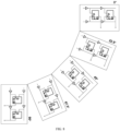
- the embodiments further provide two sensors capable of stress calibration.
- the two sensors both include a MEMS chip 1, an ASIC chip 2, and a substrate 3.
- relative position of the MEMS chip 1 and the ASIC chip 2 in the two sensors are different.
- the MEMS chip 1 is stacked with the ASIC chip 2, as shown in FIG. 1
- the MEMS chip 1 and the ASIC chip 2 are symmetrically arranged, as shown in FIG. 2 .
- FIG. 1 A stacking scheme is shown in FIG. 1 .
- the MEMS chip 1 and the ASIC chip 2 are stacked up and down in a thickness direction, the ASIC chip 2 is fixed on the substrate (not shown in the figure), and the MEMS chip 1 is stacked on a top of the ASCI chip 2.
- the MEMS chip 1 and the ASIC chip 2 are attached through gluing or bonding.
- a thickness of adhesive is less than or equal to 0.5 ⁇ m, so that the MEMS chip 1 and the ASIC chip 2 have highly consistent stress concentration characteristics.
- the MEMS chip 1 may be coaxially stacked with the ASIC chip 2, so that the MEMS chip 1 and the ASIC chip 2 have the highly consistent stress concentration characteristics.
- the ASIC chip 2 is fixed on the substrate 3 through gluing or bonding.
- a symmetrical arrangement scheme is shown in FIG. 2 .
- a center of a lower left edge of the substrate 3 is defined as a coordinate origin
- a middle major axis of a front side is defined as an x-axis
- a middle major axis of a left side is used as a y-axis.
- Both the MEMS chip 1 and the ASIC chip 2 are fixed on the substrate 3, and the center point of the MEMS chip 1, the center point of the ASIC chip 2 and the center point of the substrate 3 are on a plane parallel to the front side of the substrate 3.
- the distance from the center point M of the MEMS chip 1 to an intermediate plane of the substrate 3 is equal to the distance from the center point A of the ASIC chip 2 to the intermediate plane of the substrate 3.
- the intermediate plane is parallel to the left side and a right side of the substrate 3.
- the left side is parallel to the right side
- the front side is parallel to a rear side
- the left side is perpendicular to the front side
- a top surface is parallel to a bottom surface
- the top surface is perpendicular to both the front side and the left side.
- the MEMS chip 1 and the ASIC chip 2 are fixed on the substrate 3 in the same way, for example, may be fixed through gluing or bonding. When the MEMS chip 1 and the ASIC chip 2 are fixed through gluing, an adhesive thickness of the MEMS chip 1 is consistent with an adhesive thickness of the ASIC chip 2.
- FIG. 3 Stress calibration processing of the two sensors in the embodiment is shown in FIG. 3 .
- a structure of the ASIC chip 2 is designed, such that the ASIC chip can measure stress, and an arrangement manner of the MEMS chip 1 and the ASIC chip 2 is designed to ensure that the MEMS chip 1 and the ASIC chip 2 have highly consistent stress concentration characteristics.
- F a_z a z-axis component of resultant force obtained after thermal stress and mechanical stress act on the ASIC chip 2
- F m_z a z-axis component of resultant force on the MEMS chip 1
- F m_z there is a following relationship between the two z-axis components:
- F m _ z f
- F a _ z kF a _ z + b
- k approaches 1 and b approaches 0.
- k is related to an area ratio of the two chips, and b is a correction coefficient.
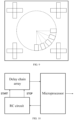
- an external capacitor C ext needs to be measured, it is only required to enable the to-be-measured external capacitor C ext and reference resistor R ref inside the RC circuit to form an external discharge circuit.
- ⁇ ext represents the discharge time of the external discharge circuit
- ⁇ ref represents the discharge time of the internal discharge circuit
- C ref represents the reference capacitor inside the RC circuit
- C ext represents the to-be-measured external capacitor
- electrical signals such as a voltage, a current, and inductance can also be converted into resistance or capacitance for measurement.
- electrical signals such as a voltage, a current, and inductance can also be converted into resistance or capacitance for measurement.
- the solution in the specific implementations can achieve high dynamics and precision. Actual measurement shows that the precision can reach at most 22 significant bits.
- this solution can greatly improve accuracy and temperature stability of the MEMS devices, and can also greatly reduce costs of packaging and calibration.
- MEMS devices that rely relatively on the size of the silicon micromechanical structure, such as a pneumatic device this solution can greatly reduce a quantity of calibration points with same accuracy, thereby significantly reducing the calibration cost.
- this solution can reduce an impact of a temperature drift by more than 90%, or lower the calibration cost by 50-70% (for the inertial MEMS devices) and 30-50% (for non-inertial MEMS devices) with the same accuracy and temperature stability.
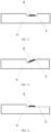
- the embodiments further provide an electric toothbrush using an ASIC chip.
- the electric toothbrush includes a brush handle and a brush head (not shown in the figure).
- a driving component is disposed in the brush handle, and output shaft 4 of the driving component is connected to the brush head.
- the electric toothbrush further includes ASIC chip 6 in the specific implementations.
- the ASIC chip 6 is disposed on the output shaft 4, the output shaft 4 is further provided with a stress triggering component, and the ASIC chip 6 is configured to detect stress at a position of the stress triggering component.
- the stress triggering component may be groove 5, and the ASIC chip 6 is located within the groove 5.
- the groove 5 has any one of a rectangular cross section, a triangular cross section, and an L-shaped cross section, as shown in FIG. 11 to FIG. 13 .
- the electric toothbrush in the specific implementations adopts a self-designed ASIC chip instead of a Wheatstone bridge whose resistance is easily to be affected by overflow of welding adhesive, and therefore effectively improves stability, reliability, sensitivity, and linearity of stress detection.
- the ASIC chip itself can achieve analog-to-digital conversion without a need for an additional analog-to-digital conversion circuit, the entire ASIC chip is located in a single temperature field, and can more accurately compensate for the temperature drift.
Landscapes
- Health & Medical Sciences (AREA)
- Physics & Mathematics (AREA)
- General Physics & Mathematics (AREA)
- Animal Behavior & Ethology (AREA)
- Life Sciences & Earth Sciences (AREA)
- General Health & Medical Sciences (AREA)
- Public Health (AREA)
- Veterinary Medicine (AREA)
- Epidemiology (AREA)
- Dentistry (AREA)
- Engineering & Computer Science (AREA)
- Microelectronics & Electronic Packaging (AREA)
- Nonlinear Science (AREA)
- Computer Hardware Design (AREA)
- Micromachines (AREA)
- Gyroscopes (AREA)
Claims (11)
- Chip für anwendungsspezifische integrierte Schaltung - ASIC - (2, 6), der in der Lage ist, Belastung zu messen, umfassend:eine Verzögerungskettenanordnung, eine Schaltung Widerstand-Kondensator - RC - und einen Mikroprozessor, wobei der Mikroprozessor ein Auslösesignal an die RC-Schaltung ausgibt, die RC-Schaltung ein erstes Signal START und ein zweites Signal STOP an einen Eingangsanschluss der Verzögerungskettenanordnung ausgibt, die Verzögerungskettenanordnung ein Zeitpropagationssignal an den Mikroprozessor ausgibt, und der Mikroprozessor das Zeitpropagationssignal zum Ausgeben eines digitalen Signals verarbeitet;wobei die Verzögerungskettenanordnung eine Vielzahl von Verzögerungsketten umfasst, dadurch gekennzeichnet, dass:
im Inneren des ASIC-Chips eine "Vier-Ecken+Mitte"-Verzögerungskette auf mindestens einer Ebene parallel zu einer Seite des ASIC-Chips angeordnet ist, eine "Vier-Ecken+Mitte"-Verzögerungskette auf mindestens einer Ebene parallel zu der anderen Seite des ASIC-Chips angeordnet ist, und eine "Vier-Ecken+Mitte"-Verzögerungskettenkombination auf mindestens einer Ebene parallel zu einer Unterseite des ASIC-Chips angeordnet ist; die zwei Seiten des ASIC-Chips senkrecht zueinander sind; und die "Vier-Ecken+Mitte"-Verzögerungskettenkombination Verzögerungsketten umfasst, die an vier Ecken einer Ebene angeordnet sind, und eine Verzögerungskette, die in einer Mitte der Ebene angeordnet ist, wobei sich die in der Mitte der Ebene angeordnete Verzögerungskette in einer anderen Ebene befindet, die sich in einem gewissen Winkel mit der Ebene schneidet. - ASIC-Chip nach Anspruch 1, wobei die Verzögerungsketten an den vier Ecken der Ebene jeweils eine beliebige von einer 90°-Verzögerungskette, einer kreuzförmigen Verzögerungskette und einer quadratischen Verzögerungskette sind, und die Verzögerungskette in der Mitte der Ebene eine beliebige von der 90°-Verzögerungskette, der kreuzförmigen Verzögerungskette, der quadratischen Verzögerungskette und einer kreisförmig verteilten Verzögerungskette ist;wobei die 90°-Verzögerungskette zwei um 90° versetzte Verzögerungsketteneinheiten umfasst;die kreuzförmige Verzögerungskette umfasst vier Verzögerungsketteneinheiten, die vier Zweige einer "kreuzförmigen" Struktur bilden, wobei sich jede der vier Verzögerungsketteneinheiten auf einem Zweig der "kreuzförmigen" Struktur befindet und die Verzögerungsketten im Uhrzeigersinn oder gegen den Uhrzeigersinn senkrecht zu der der nächsten sind;die quadratische Verzögerungskette vier Verzögerungsketteneinheiten umfasst, die vier Seiten einer "quadratischen" Struktur bilden, wobei sich jede der vier Verzögerungsketteneinheiten auf einer Seite der "quadratischen" Struktur befindet, und die Verzögerungsketten im Uhrzeigersinn oder gegen den Uhrzeigersinn senkrecht zu der der nächsten sind; unddie kreisförmig verteilte Verzögerungskette eine Vielzahl von Verzögerungsketteneinheiten umfasst, die auf einem Bogen angeordnet sind, wobei zwei benachbarte Einheiten der Vielzahl von Verzögerungsketteneinheiten in einem gewissen Winkel angeordnet sind.
- ASIC-Chip nach Anspruch 2, wobei die Verzögerungsketteneinheit eine Cursor-Verzögerungsketteneinheit, eine Abgriffsverzögerungsketteneinheit oder eine Differenzialverzögerungsketteneinheit ist.
- Sensor unter Verwendung eines ASIC-Chips, umfassend ein Substrat (3) und einen Chip für mikro-elektromechanisches System - MEMS - (1), wobei der Sensor ferner den ASIC-Chip (2) nach einem der Ansprüche 1 bis 3 umfasst, der ASIC-Chip (2) auf dem Substrat (3) befestigt ist und der MEMS-Chip (1) auf einer Oberseite des ASIC-Chips (2) gestapelt ist.
- Sensor unter Verwendung des ASIC-Chips nach Anspruch 4, wobei der MEMS-Chip (1) und der ASIC-Chip (2) durch Kleben oder Bonden angebracht sind; und wenn der MEMS-Chip (1) und der ASIC-Chip (2) durch Kleben angebracht sind, eine Stärke des Klebstoffs weniger als oder gleich wie 0,5 µm ist.
- Sensor unter Verwendung des ASIC-Chips nach Anspruch 4, wobei der MEMS-Chip (1) koaxial mit dem ASIC-Chip (2) gestapelt ist.
- Sensor unter Verwendung eines ASIC-Chips, umfassend ein Substrat (3) und einen MEMS-Chip (1), wobei der Sensor ferner den ASIC-Chip (2) nach einem der Ansprüche 1 bis 3 umfasst, wobei sowohl der MEMS-Chip (1) als auch der ASIC-Chip (2) auf dem Substrat (3) befestigt sind, wobei der Mittelpunkt des MEMS-Chips (1), ein Mittelpunkt des ASIC-Chips (2) und ein Mittelpunkt des Substrats (3) auf einer Ebene parallel zu einer Seite des Substrats (3) sind, ein Abstand zwischen dem Mittelpunkt des MEMS-Chips (1) und einer Zwischenebene des Substrats (3) gleich wie ein Abstand zwischen dem Mittelpunkt des ASIC-Chips (2) und der Zwischenebene des Substrats (3) ist, die Zwischenebene eine Zwischenebene parallel zu der anderen Seite des Substrats ist, und die zwei Seiten des Substrats senkrecht zueinander sind.
- Sensor unter Verwendung des ASIC-Chips nach Anspruch 7, wobei sowohl der MEMS-Chip (1) als auch der ASIC-Chip (2) durch Kleben oder Bonden auf dem Substrat (3) befestigt sind; und wenn der MEMS-Chip (1) und der ASIC-Chip (2) durch Kleben auf dem Substrat (3) befestigt sind, die Klebstoffstärke des MEMS-Chips (1) mit der Klebstoffstärke des ASIC-Chips (2) konsistent ist.
- Elektrische Zahnbürste unter Verwendung eines ASIC-Chips, umfassend einen Bürstengriff und einen Bürstenkopf, wobei eine Antriebskomponente in dem Bürstengriff angeordnet ist und eine Ausgangswelle (4) der Antriebskomponente mit dem Bürstenkopf verbunden ist; und wobei die elektrische Zahnbürste ferner den ASIC-Chip (6) nach einem der Ansprüche 1 bis 3 umfasst, wobei der ASIC-Chip (6) auf der Ausgangswelle (4) angeordnet ist, die Ausgangswelle ferner mit einer Spannungsauslösekomponente versehen ist und der ASIC-Chip (6) konfiguriert ist, um Belastung an einer Position der Belastungsauslösekomponente zu erfassen.
- Elektrische Zahnbürste unter Verwendung des ASIC-Chips nach Anspruch 9, wobei die Belastungsauslösekomponente eine Nut (5) ist, die auf einer Oberfläche der Ausgangswelle (4) angeordnet ist, und der ASIC-Chip (6) innerhalb der Nut (5) angeordnet ist.
- Elektrische Zahnbürste unter Verwendung des ASIC-Chips nach Anspruch 10, wobei die Nut (5) einen beliebigen von einem rechteckigen Querschnitt, einem dreieckigen Querschnitt oder einem L-förmigen Querschnitt aufweist.
Applications Claiming Priority (2)
| Application Number | Priority Date | Filing Date | Title |
|---|---|---|---|
| CN202211075505.5A CN115137517B (zh) | 2022-09-05 | 2022-09-05 | Asic芯片及使用其的传感器、电动牙刷 |
| PCT/CN2022/122754 WO2024050900A1 (zh) | 2022-09-05 | 2022-09-29 | Asic芯片及使用其的传感器、电动牙刷 |
Publications (4)
| Publication Number | Publication Date |
|---|---|
| EP4358152A1 EP4358152A1 (de) | 2024-04-24 |
| EP4358152A4 EP4358152A4 (de) | 2024-09-11 |
| EP4358152B1 true EP4358152B1 (de) | 2025-04-09 |
| EP4358152B8 EP4358152B8 (de) | 2025-06-18 |
Family
ID=90060093
Family Applications (1)
| Application Number | Title | Priority Date | Filing Date |
|---|---|---|---|
| EP22922577.6A Active EP4358152B8 (de) | 2022-09-05 | 2022-09-29 | Anwendungsspezifischer chip mit integrierter schaltung (asic) sowie sensor und elektrische zahnbürste damit |
Country Status (3)
| Country | Link |
|---|---|
| US (1) | US11973503B2 (de) |
| EP (1) | EP4358152B8 (de) |
| KR (1) | KR20240035736A (de) |
Family Cites Families (7)
| Publication number | Priority date | Publication date | Assignee | Title |
|---|---|---|---|---|
| US7254505B2 (en) * | 2005-06-29 | 2007-08-07 | Avago Technologies General Ip (Singapore) Pte. Ltd. | Method and apparatus for calibrating delay lines |
| DE102007026684B4 (de) * | 2007-06-08 | 2009-03-19 | Gesellschaft für Schwerionenforschung mbH | Zeit-Amplituden-Konverter-Bauelement |
| JP4512125B2 (ja) * | 2007-09-07 | 2010-07-28 | 株式会社リコー | 応力分布検出用半導体パッケージ群及びそれを用いた半導体パッケージの応力分布検出方法 |
| US8823388B2 (en) * | 2011-06-03 | 2014-09-02 | Solid State System Co., Ltd. | Calibration circuit and calibration method |
| CN108309486B (zh) | 2017-12-21 | 2024-01-30 | 深圳瑞浒科技有限公司 | 带有检测刷头压力装置的电动牙刷 |
| CN109738109B (zh) | 2019-01-31 | 2024-02-13 | 南京信息工程大学 | 一种高温微压压力传感器及其制作方法、测量系统 |
| EP3772640B1 (de) | 2019-08-09 | 2022-06-22 | Sciosense B.V. | Elektrische schaltungsanordnung zur dehnungsmessung |
-
2022
- 2022-09-29 EP EP22922577.6A patent/EP4358152B8/de active Active
- 2022-09-29 US US18/277,098 patent/US11973503B2/en active Active
- 2022-09-29 KR KR1020237020771A patent/KR20240035736A/ko active Pending
Also Published As
| Publication number | Publication date |
|---|---|
| EP4358152A1 (de) | 2024-04-24 |
| US20240080021A1 (en) | 2024-03-07 |
| EP4358152A4 (de) | 2024-09-11 |
| US11973503B2 (en) | 2024-04-30 |
| KR20240035736A (ko) | 2024-03-18 |
| EP4358152B8 (de) | 2025-06-18 |
Similar Documents
| Publication | Publication Date | Title |
|---|---|---|
| US7500406B2 (en) | Multiaxial sensor | |
| US5035148A (en) | Force detector using resistance elements | |
| US20090013755A1 (en) | Calibration jig and algorithms for accelerometer | |
| US7428841B2 (en) | Acceleration sensor and inclination-detecting method | |
| CN101216498A (zh) | 一种双轴差动电容式微机械加速度计 | |
| US12072254B2 (en) | Electric circuitry with differently oriented ring oscillators for strain measurement | |
| US11920993B1 (en) | Miniature combined multi-axis force sensor structure | |
| EP4358152B1 (de) | Anwendungsspezifischer chip mit integrierter schaltung (asic) sowie sensor und elektrische zahnbürste damit | |
| KR20140067650A (ko) | 토크 센서 | |
| RU2362236C1 (ru) | Матрица интегральных преобразователей давления | |
| CN110531443B (zh) | 一种地震烈度仪的标定装置 | |
| EP3323778B1 (de) | Mems-vorrichtung und verfahren zur kalibrierung einer mems-vorrichtung | |
| CN115137517B (zh) | Asic芯片及使用其的传感器、电动牙刷 | |
| JP3020736B2 (ja) | 静電容量の変化を利用したセンサ用の信号処理回路 | |
| CN117629492A (zh) | 一种基于mems工艺的硅压阻式六维力传感器及其制备方法 | |
| JPH09210690A (ja) | 角速度検出センサ | |
| CN103239217A (zh) | 防过载的脉搏跳动血压波强度传感器 | |
| CN219064410U (zh) | 一种高精度应变测量传感器 | |
| JPH0526754A (ja) | 静電容量の変化を利用したセンサ | |
| Herrmann et al. | Design and characterization of in-plane silicon stress sensors with isotropic sensitivity | |
| CN116124318B (zh) | 一种基于二自由度谐振器的谐振式温度传感器及其制备方法 | |
| KR100295622B1 (ko) | 진동/온도 복합센서 | |
| JPH0830716B2 (ja) | 半導体加速度検出装置 | |
| CN203169161U (zh) | 防过载的脉搏跳动血压波强度传感器 | |
| JPH0231812B2 (de) |
Legal Events
| Date | Code | Title | Description |
|---|---|---|---|
| STAA | Information on the status of an ep patent application or granted ep patent |
Free format text: STATUS: UNKNOWN |
|
| STAA | Information on the status of an ep patent application or granted ep patent |
Free format text: STATUS: THE INTERNATIONAL PUBLICATION HAS BEEN MADE |
|
| PUAI | Public reference made under article 153(3) epc to a published international application that has entered the european phase |
Free format text: ORIGINAL CODE: 0009012 |
|
| STAA | Information on the status of an ep patent application or granted ep patent |
Free format text: STATUS: REQUEST FOR EXAMINATION WAS MADE |
|
| 17P | Request for examination filed |
Effective date: 20230804 |
|
| AK | Designated contracting states |
Kind code of ref document: A1 Designated state(s): AL AT BE BG CH CY CZ DE DK EE ES FI FR GB GR HR HU IE IS IT LI LT LU LV MC MK MT NL NO PL PT RO RS SE SI SK SM TR |
|
| RBV | Designated contracting states (corrected) |
Designated state(s): AL AT BE BG CH CY CZ DE DK EE ES FI FR GB GR HR HU IE IS IT LI LT LU LV MC MK MT NL NO PL PT RO RS SE SI SK SM TR |
|
| REG | Reference to a national code |
Ref country code: DE Ref legal event code: R079 Free format text: PREVIOUS MAIN CLASS: H01L0029660000 Ipc: H03K0005133000 Ref document number: 602022013072 Country of ref document: DE |
|
| STAA | Information on the status of an ep patent application or granted ep patent |
Free format text: STATUS: EXAMINATION IS IN PROGRESS |
|
| A4 | Supplementary search report drawn up and despatched |
Effective date: 20240812 |
|
| RIC1 | Information provided on ipc code assigned before grant |
Ipc: H03K 5/133 20140101AFI20240806BHEP |
|
| 17Q | First examination report despatched |
Effective date: 20240823 |
|
| RIC1 | Information provided on ipc code assigned before grant |
Ipc: A61C 17/22 20060101ALI20241219BHEP Ipc: A46B 15/00 20060101ALI20241219BHEP Ipc: G01L 25/00 20060101ALI20241219BHEP Ipc: G01L 5/16 20200101ALI20241219BHEP Ipc: H03K 5/133 20140101AFI20241219BHEP |
|
| GRAP | Despatch of communication of intention to grant a patent |
Free format text: ORIGINAL CODE: EPIDOSNIGR1 |
|
| STAA | Information on the status of an ep patent application or granted ep patent |
Free format text: STATUS: GRANT OF PATENT IS INTENDED |
|
| DAV | Request for validation of the european patent (deleted) | ||
| DAX | Request for extension of the european patent (deleted) | ||
| INTG | Intention to grant announced |
Effective date: 20250124 |
|
| GRAS | Grant fee paid |
Free format text: ORIGINAL CODE: EPIDOSNIGR3 |
|
| GRAA | (expected) grant |
Free format text: ORIGINAL CODE: 0009210 |
|
| STAA | Information on the status of an ep patent application or granted ep patent |
Free format text: STATUS: THE PATENT HAS BEEN GRANTED |
|
| AK | Designated contracting states |
Kind code of ref document: B1 Designated state(s): AL AT BE BG CH CY CZ DE DK EE ES FI FR GB GR HR HU IE IS IT LI LT LU LV MC MK MT NL NO PL PT RO RS SE SI SK SM TR |
|
| REG | Reference to a national code |
Ref country code: GB Ref legal event code: FG4D |
|
| REG | Reference to a national code |
Ref country code: CH Ref legal event code: EP |
|
| REG | Reference to a national code |
Ref country code: DE Ref legal event code: R096 Ref document number: 602022013072 Country of ref document: DE |
|
| GRAT | Correction requested after decision to grant or after decision to maintain patent in amended form |
Free format text: ORIGINAL CODE: EPIDOSNCDEC |
|
| REG | Reference to a national code |
Ref country code: IE Ref legal event code: FG4D |
|
| REG | Reference to a national code |
Ref country code: CH Ref legal event code: PK Free format text: BERICHTIGUNG B8 |
|
| REG | Reference to a national code |
Ref country code: NL Ref legal event code: MP Effective date: 20250409 |
|
| PG25 | Lapsed in a contracting state [announced via postgrant information from national office to epo] |
Ref country code: NL Free format text: LAPSE BECAUSE OF FAILURE TO SUBMIT A TRANSLATION OF THE DESCRIPTION OR TO PAY THE FEE WITHIN THE PRESCRIBED TIME-LIMIT Effective date: 20250409 |
|
| REG | Reference to a national code |
Ref country code: AT Ref legal event code: MK05 Ref document number: 1784472 Country of ref document: AT Kind code of ref document: T Effective date: 20250409 |
|
| PG25 | Lapsed in a contracting state [announced via postgrant information from national office to epo] |
Ref country code: FI Free format text: LAPSE BECAUSE OF FAILURE TO SUBMIT A TRANSLATION OF THE DESCRIPTION OR TO PAY THE FEE WITHIN THE PRESCRIBED TIME-LIMIT Effective date: 20250409 Ref country code: PT Free format text: LAPSE BECAUSE OF FAILURE TO SUBMIT A TRANSLATION OF THE DESCRIPTION OR TO PAY THE FEE WITHIN THE PRESCRIBED TIME-LIMIT Effective date: 20250811 Ref country code: ES Free format text: LAPSE BECAUSE OF FAILURE TO SUBMIT A TRANSLATION OF THE DESCRIPTION OR TO PAY THE FEE WITHIN THE PRESCRIBED TIME-LIMIT Effective date: 20250409 |
|
| PGFP | Annual fee paid to national office [announced via postgrant information from national office to epo] |
Ref country code: DE Payment date: 20250919 Year of fee payment: 4 |
|
| REG | Reference to a national code |
Ref country code: LT Ref legal event code: MG9D |
|
| PG25 | Lapsed in a contracting state [announced via postgrant information from national office to epo] |
Ref country code: NO Free format text: LAPSE BECAUSE OF FAILURE TO SUBMIT A TRANSLATION OF THE DESCRIPTION OR TO PAY THE FEE WITHIN THE PRESCRIBED TIME-LIMIT Effective date: 20250709 Ref country code: GR Free format text: LAPSE BECAUSE OF FAILURE TO SUBMIT A TRANSLATION OF THE DESCRIPTION OR TO PAY THE FEE WITHIN THE PRESCRIBED TIME-LIMIT Effective date: 20250710 |
|
| PG25 | Lapsed in a contracting state [announced via postgrant information from national office to epo] |
Ref country code: PL Free format text: LAPSE BECAUSE OF FAILURE TO SUBMIT A TRANSLATION OF THE DESCRIPTION OR TO PAY THE FEE WITHIN THE PRESCRIBED TIME-LIMIT Effective date: 20250409 |
|
| PG25 | Lapsed in a contracting state [announced via postgrant information from national office to epo] |
Ref country code: BG Free format text: LAPSE BECAUSE OF FAILURE TO SUBMIT A TRANSLATION OF THE DESCRIPTION OR TO PAY THE FEE WITHIN THE PRESCRIBED TIME-LIMIT Effective date: 20250409 |
|
| PG25 | Lapsed in a contracting state [announced via postgrant information from national office to epo] |
Ref country code: HR Free format text: LAPSE BECAUSE OF FAILURE TO SUBMIT A TRANSLATION OF THE DESCRIPTION OR TO PAY THE FEE WITHIN THE PRESCRIBED TIME-LIMIT Effective date: 20250409 |
|
| PG25 | Lapsed in a contracting state [announced via postgrant information from national office to epo] |
Ref country code: AT Free format text: LAPSE BECAUSE OF FAILURE TO SUBMIT A TRANSLATION OF THE DESCRIPTION OR TO PAY THE FEE WITHIN THE PRESCRIBED TIME-LIMIT Effective date: 20250409 |
|
| PGFP | Annual fee paid to national office [announced via postgrant information from national office to epo] |
Ref country code: FR Payment date: 20250922 Year of fee payment: 4 |
|
| PG25 | Lapsed in a contracting state [announced via postgrant information from national office to epo] |
Ref country code: RS Free format text: LAPSE BECAUSE OF FAILURE TO SUBMIT A TRANSLATION OF THE DESCRIPTION OR TO PAY THE FEE WITHIN THE PRESCRIBED TIME-LIMIT Effective date: 20250709 |
|
| PG25 | Lapsed in a contracting state [announced via postgrant information from national office to epo] |
Ref country code: IS Free format text: LAPSE BECAUSE OF FAILURE TO SUBMIT A TRANSLATION OF THE DESCRIPTION OR TO PAY THE FEE WITHIN THE PRESCRIBED TIME-LIMIT Effective date: 20250809 |
|
| PG25 | Lapsed in a contracting state [announced via postgrant information from national office to epo] |
Ref country code: LV Free format text: LAPSE BECAUSE OF FAILURE TO SUBMIT A TRANSLATION OF THE DESCRIPTION OR TO PAY THE FEE WITHIN THE PRESCRIBED TIME-LIMIT Effective date: 20250409 |