EP4354570A2 - Batteriepack mit wärmeableitungsstruktur - Google Patents
Batteriepack mit wärmeableitungsstruktur Download PDFInfo
- Publication number
- EP4354570A2 EP4354570A2 EP23194378.8A EP23194378A EP4354570A2 EP 4354570 A2 EP4354570 A2 EP 4354570A2 EP 23194378 A EP23194378 A EP 23194378A EP 4354570 A2 EP4354570 A2 EP 4354570A2
- Authority
- EP
- European Patent Office
- Prior art keywords
- heat dissipation
- battery pack
- heat
- fixing
- protection circuit
- Prior art date
- Legal status (The legal status is an assumption and is not a legal conclusion. Google has not performed a legal analysis and makes no representation as to the accuracy of the status listed.)
- Pending
Links
Images




Classifications
-
- H—ELECTRICITY
- H01—ELECTRIC ELEMENTS
- H01M—PROCESSES OR MEANS, e.g. BATTERIES, FOR THE DIRECT CONVERSION OF CHEMICAL ENERGY INTO ELECTRICAL ENERGY
- H01M10/00—Secondary cells; Manufacture thereof
- H01M10/42—Methods or arrangements for servicing or maintenance of secondary cells or secondary half-cells
- H01M10/425—Structural combination with electronic components, e.g. electronic circuits integrated to the outside of the casing
-
- H—ELECTRICITY
- H01—ELECTRIC ELEMENTS
- H01M—PROCESSES OR MEANS, e.g. BATTERIES, FOR THE DIRECT CONVERSION OF CHEMICAL ENERGY INTO ELECTRICAL ENERGY
- H01M50/00—Constructional details or processes of manufacture of the non-active parts of electrochemical cells other than fuel cells, e.g. hybrid cells
- H01M50/20—Mountings; Secondary casings or frames; Racks, modules or packs; Suspension devices; Shock absorbers; Transport or carrying devices; Holders
- H01M50/271—Lids or covers for the racks or secondary casings
-
- H—ELECTRICITY
- H10—SEMICONDUCTOR DEVICES; ELECTRIC SOLID-STATE DEVICES NOT OTHERWISE PROVIDED FOR
- H10W—GENERIC PACKAGES, INTERCONNECTIONS, CONNECTORS OR OTHER CONSTRUCTIONAL DETAILS OF DEVICES COVERED BY CLASS H10
- H10W40/00—Arrangements for thermal protection or thermal control
- H10W40/20—Arrangements for cooling
- H10W40/25—Arrangements for cooling characterised by their materials
- H10W40/258—Metallic materials
-
- H—ELECTRICITY
- H01—ELECTRIC ELEMENTS
- H01M—PROCESSES OR MEANS, e.g. BATTERIES, FOR THE DIRECT CONVERSION OF CHEMICAL ENERGY INTO ELECTRICAL ENERGY
- H01M10/00—Secondary cells; Manufacture thereof
- H01M10/60—Heating or cooling; Temperature control
- H01M10/66—Heat-exchange relationships between the cells and other systems, e.g. central heating systems or fuel cells
- H01M10/667—Heat-exchange relationships between the cells and other systems, e.g. central heating systems or fuel cells the system being an electronic component, e.g. a CPU, an inverter or a capacitor
-
- H—ELECTRICITY
- H01—ELECTRIC ELEMENTS
- H01M—PROCESSES OR MEANS, e.g. BATTERIES, FOR THE DIRECT CONVERSION OF CHEMICAL ENERGY INTO ELECTRICAL ENERGY
- H01M10/00—Secondary cells; Manufacture thereof
- H01M10/04—Construction or manufacture in general
- H01M10/0431—Cells with wound or folded electrodes
-
- H—ELECTRICITY
- H01—ELECTRIC ELEMENTS
- H01M—PROCESSES OR MEANS, e.g. BATTERIES, FOR THE DIRECT CONVERSION OF CHEMICAL ENERGY INTO ELECTRICAL ENERGY
- H01M10/00—Secondary cells; Manufacture thereof
- H01M10/04—Construction or manufacture in general
- H01M10/0436—Small-sized flat cells or batteries for portable equipment
-
- H—ELECTRICITY
- H01—ELECTRIC ELEMENTS
- H01M—PROCESSES OR MEANS, e.g. BATTERIES, FOR THE DIRECT CONVERSION OF CHEMICAL ENERGY INTO ELECTRICAL ENERGY
- H01M10/00—Secondary cells; Manufacture thereof
- H01M10/42—Methods or arrangements for servicing or maintenance of secondary cells or secondary half-cells
-
- H—ELECTRICITY
- H01—ELECTRIC ELEMENTS
- H01M—PROCESSES OR MEANS, e.g. BATTERIES, FOR THE DIRECT CONVERSION OF CHEMICAL ENERGY INTO ELECTRICAL ENERGY
- H01M10/00—Secondary cells; Manufacture thereof
- H01M10/42—Methods or arrangements for servicing or maintenance of secondary cells or secondary half-cells
- H01M10/425—Structural combination with electronic components, e.g. electronic circuits integrated to the outside of the casing
- H01M10/4257—Smart batteries, e.g. electronic circuits inside the housing of the cells or batteries
-
- H—ELECTRICITY
- H01—ELECTRIC ELEMENTS
- H01M—PROCESSES OR MEANS, e.g. BATTERIES, FOR THE DIRECT CONVERSION OF CHEMICAL ENERGY INTO ELECTRICAL ENERGY
- H01M10/00—Secondary cells; Manufacture thereof
- H01M10/60—Heating or cooling; Temperature control
- H01M10/61—Types of temperature control
- H01M10/613—Cooling or keeping cold
-
- H—ELECTRICITY
- H01—ELECTRIC ELEMENTS
- H01M—PROCESSES OR MEANS, e.g. BATTERIES, FOR THE DIRECT CONVERSION OF CHEMICAL ENERGY INTO ELECTRICAL ENERGY
- H01M10/00—Secondary cells; Manufacture thereof
- H01M10/60—Heating or cooling; Temperature control
- H01M10/64—Heating or cooling; Temperature control characterised by the shape of the cells
- H01M10/647—Prismatic or flat cells, e.g. pouch cells
-
- H—ELECTRICITY
- H01—ELECTRIC ELEMENTS
- H01M—PROCESSES OR MEANS, e.g. BATTERIES, FOR THE DIRECT CONVERSION OF CHEMICAL ENERGY INTO ELECTRICAL ENERGY
- H01M10/00—Secondary cells; Manufacture thereof
- H01M10/60—Heating or cooling; Temperature control
- H01M10/65—Means for temperature control structurally associated with the cells
- H01M10/655—Solid structures for heat exchange or heat conduction
-
- H—ELECTRICITY
- H01—ELECTRIC ELEMENTS
- H01M—PROCESSES OR MEANS, e.g. BATTERIES, FOR THE DIRECT CONVERSION OF CHEMICAL ENERGY INTO ELECTRICAL ENERGY
- H01M10/00—Secondary cells; Manufacture thereof
- H01M10/60—Heating or cooling; Temperature control
- H01M10/65—Means for temperature control structurally associated with the cells
- H01M10/655—Solid structures for heat exchange or heat conduction
- H01M10/6551—Surfaces specially adapted for heat dissipation or radiation, e.g. fins or coatings
-
- H—ELECTRICITY
- H01—ELECTRIC ELEMENTS
- H01M—PROCESSES OR MEANS, e.g. BATTERIES, FOR THE DIRECT CONVERSION OF CHEMICAL ENERGY INTO ELECTRICAL ENERGY
- H01M10/00—Secondary cells; Manufacture thereof
- H01M10/60—Heating or cooling; Temperature control
- H01M10/65—Means for temperature control structurally associated with the cells
- H01M10/655—Solid structures for heat exchange or heat conduction
- H01M10/6553—Terminals or leads
-
- H—ELECTRICITY
- H01—ELECTRIC ELEMENTS
- H01M—PROCESSES OR MEANS, e.g. BATTERIES, FOR THE DIRECT CONVERSION OF CHEMICAL ENERGY INTO ELECTRICAL ENERGY
- H01M10/00—Secondary cells; Manufacture thereof
- H01M10/60—Heating or cooling; Temperature control
- H01M10/65—Means for temperature control structurally associated with the cells
- H01M10/655—Solid structures for heat exchange or heat conduction
- H01M10/6554—Rods or plates
-
- H—ELECTRICITY
- H01—ELECTRIC ELEMENTS
- H01M—PROCESSES OR MEANS, e.g. BATTERIES, FOR THE DIRECT CONVERSION OF CHEMICAL ENERGY INTO ELECTRICAL ENERGY
- H01M50/00—Constructional details or processes of manufacture of the non-active parts of electrochemical cells other than fuel cells, e.g. hybrid cells
- H01M50/20—Mountings; Secondary casings or frames; Racks, modules or packs; Suspension devices; Shock absorbers; Transport or carrying devices; Holders
- H01M50/284—Mountings; Secondary casings or frames; Racks, modules or packs; Suspension devices; Shock absorbers; Transport or carrying devices; Holders with incorporated circuit boards, e.g. printed circuit boards [PCB]
- H01M50/287—Fixing of circuit boards to lids or covers
-
- H—ELECTRICITY
- H01—ELECTRIC ELEMENTS
- H01M—PROCESSES OR MEANS, e.g. BATTERIES, FOR THE DIRECT CONVERSION OF CHEMICAL ENERGY INTO ELECTRICAL ENERGY
- H01M50/00—Constructional details or processes of manufacture of the non-active parts of electrochemical cells other than fuel cells, e.g. hybrid cells
- H01M50/50—Current conducting connections for cells or batteries
- H01M50/531—Electrode connections inside a battery casing
-
- H—ELECTRICITY
- H01—ELECTRIC ELEMENTS
- H01M—PROCESSES OR MEANS, e.g. BATTERIES, FOR THE DIRECT CONVERSION OF CHEMICAL ENERGY INTO ELECTRICAL ENERGY
- H01M50/00—Constructional details or processes of manufacture of the non-active parts of electrochemical cells other than fuel cells, e.g. hybrid cells
- H01M50/50—Current conducting connections for cells or batteries
- H01M50/572—Means for preventing undesired use or discharge
- H01M50/574—Devices or arrangements for the interruption of current
-
- H—ELECTRICITY
- H10—SEMICONDUCTOR DEVICES; ELECTRIC SOLID-STATE DEVICES NOT OTHERWISE PROVIDED FOR
- H10W—GENERIC PACKAGES, INTERCONNECTIONS, CONNECTORS OR OTHER CONSTRUCTIONAL DETAILS OF DEVICES COVERED BY CLASS H10
- H10W40/00—Arrangements for thermal protection or thermal control
- H10W40/20—Arrangements for cooling
- H10W40/22—Arrangements for cooling characterised by their shape, e.g. having conical or cylindrical projections
-
- H—ELECTRICITY
- H01—ELECTRIC ELEMENTS
- H01M—PROCESSES OR MEANS, e.g. BATTERIES, FOR THE DIRECT CONVERSION OF CHEMICAL ENERGY INTO ELECTRICAL ENERGY
- H01M10/00—Secondary cells; Manufacture thereof
- H01M10/42—Methods or arrangements for servicing or maintenance of secondary cells or secondary half-cells
- H01M10/425—Structural combination with electronic components, e.g. electronic circuits integrated to the outside of the casing
- H01M2010/4271—Battery management systems including electronic circuits, e.g. control of current or voltage to keep battery in healthy state, cell balancing
-
- H—ELECTRICITY
- H01—ELECTRIC ELEMENTS
- H01M—PROCESSES OR MEANS, e.g. BATTERIES, FOR THE DIRECT CONVERSION OF CHEMICAL ENERGY INTO ELECTRICAL ENERGY
- H01M2200/00—Safety devices for primary or secondary batteries
-
- H—ELECTRICITY
- H01—ELECTRIC ELEMENTS
- H01M—PROCESSES OR MEANS, e.g. BATTERIES, FOR THE DIRECT CONVERSION OF CHEMICAL ENERGY INTO ELECTRICAL ENERGY
- H01M50/00—Constructional details or processes of manufacture of the non-active parts of electrochemical cells other than fuel cells, e.g. hybrid cells
- H01M50/20—Mountings; Secondary casings or frames; Racks, modules or packs; Suspension devices; Shock absorbers; Transport or carrying devices; Holders
- H01M50/202—Casings or frames around the primary casing of a single cell or a single battery
-
- H—ELECTRICITY
- H02—GENERATION; CONVERSION OR DISTRIBUTION OF ELECTRIC POWER
- H02J—ELECTRIC POWER NETWORKS; CIRCUIT ARRANGEMENTS OR SYSTEMS FOR SUPPLYING OR DISTRIBUTING ELECTRIC POWER; SYSTEMS FOR STORING ELECTRIC ENERGY
- H02J7/00—Circuit arrangements for charging or discharging batteries or for supplying loads from batteries
- H02J7/60—Circuit arrangements for charging or discharging batteries or for supplying loads from batteries including safety or protection arrangements
-
- Y—GENERAL TAGGING OF NEW TECHNOLOGICAL DEVELOPMENTS; GENERAL TAGGING OF CROSS-SECTIONAL TECHNOLOGIES SPANNING OVER SEVERAL SECTIONS OF THE IPC; TECHNICAL SUBJECTS COVERED BY FORMER USPC CROSS-REFERENCE ART COLLECTIONS [XRACs] AND DIGESTS
- Y02—TECHNOLOGIES OR APPLICATIONS FOR MITIGATION OR ADAPTATION AGAINST CLIMATE CHANGE
- Y02E—REDUCTION OF GREENHOUSE GAS [GHG] EMISSIONS, RELATED TO ENERGY GENERATION, TRANSMISSION OR DISTRIBUTION
- Y02E60/00—Enabling technologies; Technologies with a potential or indirect contribution to GHG emissions mitigation
- Y02E60/10—Energy storage using batteries
Definitions
- One or more embodiments relate to a battery pack including a heat dissipation structure.
- each battery pack generally includes an electrode assembly including a positive electrode, a negative electrode, and a separator, and a case for accommodating the electrode assembly.
- a pouch-type battery pack accommodates an electrode assembly wound in the form of a jelly roll, or an electrode assembly stacked in the form of a stack cell in a case, and includes a protection circuit module for reducing or preventing the likelihood of overcharging, overdischarging, or overcurrent of the battery pack.
- the battery pack includes a separate case or tape as a fixing bracket for fixing the electrode assembly.
- the battery pack may be heated to a relatively high temperature as charging and discharging are repeated.
- a field effect transistor (FET) of a protection circuit module is the biggest factor of heat emission. Heat generated by an FET is transferred to the entire battery pack as well as a protection circuit module, and may deteriorate the characteristics of the battery pack.
- One or more embodiments include a battery pack that enables heat generated by a field effect transistor in a protection circuit module to be dissipated without it being transferred to the entire battery pack.
- a battery pack includes a case, an electrode assembly in the case, and including an electrode tab, a protection circuit module connected to the electrode tab, a fixing bracket at least partially surrounding the protection circuit module, and a heat dissipator outside the fixing bracket and including a heat dissipation element.
- the heat dissipation element may include a pair of elements respectively corresponding to an upper surface of the protection circuit module, and to a lower surface of the protection circuit module.
- the heat dissipation element may include a metal layer including aluminium.
- the fixing bracket may include a first fixing surface abutting an upper surface of the protection circuit module, a second fixing surface extending downward from an end portion of the first fixing surface, and abutting a side surface of the protection circuit module, and a third fixing surface extending toward the case from an end portion of the second fixing surface, and abutting a lower surface of the protection circuit module, wherein the heat dissipator includes a first heat dissipation surface, a second heat dissipation surface, and a third heat dissipation surface, which respectively correspond to the first fixing surface, the second fixing surface, and the third fixing surface.
- the heat dissipation element may be at an interior of the first heat dissipation surface, and is at an interior of the third heat dissipation surface.
- Both ends of the first heat dissipation surface may contact one surface of the first fixing surface, and define a heat insulation space between the heat dissipation element and the first heat dissipation surface, wherein both ends of the third heat dissipation surface contact one surface of the third fixing surface, and define a heat insulation space between the heat dissipation element and the third heat dissipation surface.
- the heat dissipation element may be at an interior of the second heat dissipation surface.
- the protection circuit module may include field effect transistors (FET), wherein the heat dissipator covers the FETs.
- FET field effect transistors
- the FETs may be inside the heat dissipator in a plan view.
- An area of the heat dissipator may be greater than a sum of areas of the FETs.
- the heat dissipation element may be detachably arranged on the heat dissipator.
- the heat dissipation element may be integrally formed with the heat dissipator to be coplanar with the heat dissipator.
- the heat dissipator may contact the fixing bracket.
- an implanted region illustrated as a rectangle may have rounded or curved features and/or a gradient of implant concentration at its edges rather than a binary change from implanted to non-implanted region.
- a buried region formed by implantation may result in some implantation in the region between the buried region and the surface through which the implantation takes place.
- spatially relative terms such as “beneath,” “below,” “lower,” “lower side,” “under,” “above,” “upper,” “upper side,” and the like, may be used herein for ease of explanation to describe one element or feature's relationship to another element(s) or feature(s) as illustrated in the figures. It will be understood that the spatially relative terms are intended to encompass different orientations of the device in use or in operation, in addition to the orientation depicted in the figures. For example, if the device in the figures is turned over, elements described as “below,” “beneath,” “or “under” other elements or features would then be oriented “above” the other elements or features. Thus, the example terms “below” and “under” can encompass both an orientation of above and below.
- the device may be otherwise oriented (e.g., rotated 90 degrees or at other orientations) and the spatially relative descriptors used herein should be interpreted accordingly.
- first part is described as being arranged "on" a second part, this indicates that the first part is arranged at an upper side or a lower side of the second part without the limitation to the upper side thereof on the basis of the gravity direction.
- the phrase “in a plan view” means when an object portion is viewed from above
- the phrase “in a schematic cross-sectional view” means when a schematic cross-section taken by vertically cutting an object portion is viewed from the side.
- overlap or “overlapped” mean that a first object may be above or below or to a side of a second object, and vice versa.
- overlap may include layer, stack, face or facing, extending over, covering, or partly covering or any other suitable term as would be appreciated and understood by those of ordinary skill in the art.
- not overlap may include meaning, such as “apart from” or “set aside from” or “offset from” and any other suitable equivalents as would be appreciated and understood by those of ordinary skill in the art.
- face and “facing” may mean that a first object may directly or indirectly oppose a second object. In a case in which a third object intervenes between a first and second object, the first and second objects may be understood as being indirectly opposed to one another, although still facing each other.
- a layer, region, or component when referred to as being “electrically connected” or “electrically coupled” to another layer, region, or component, it can be directly electrically connected or coupled to the other layer, region, and/or component or intervening layers, regions, or components may be present.
- directly connected/directly coupled or “directly on,” refers to one component directly connecting or coupling another component, or being on another component, without an intermediate component.
- a forming direction is not limited to an upper direction but includes forming the portion on a side surface or in a lower direction.
- “at least one of X, Y, and Z,” “at least one of X, Y, or Z,” “at least one selected from the group consisting of X, Y, and Z,” and “at least one selected from the group consisting of X, Y, or Z” may be construed as X only, Y only, Z only, any combination of two or more of X, Y, and Z, such as, for instance, XYZ, XYY, YZ, and ZZ, or any variation thereof.
- the expression such as “at least one of A and B” and “at least one of A or B” may include A, B, or A and B.
- “or” generally means “and/or,” and the term “and/or” includes any and all combinations of one or more of the associated listed items.
- the expression such as “A and/or B” may include A, B, or A and B.
- first,” “second,” “third,” etc. may be used herein to describe various elements, components, regions, layers and/or sections, these elements, components, regions, layers and/or sections should not be limited by these terms. These terms are used to distinguish one element, component, region, layer or section from another element, component, region, layer or section. Thus, a first element, component, region, layer or section described below could be termed a second element, component, region, layer or section, without departing from the scope of the present disclosure. The description of an element as a “first” element may not require or imply the presence of a second element or other elements.
- the terms “first,” “second,” etc. may also be used herein to differentiate different categories or sets of elements. For conciseness, the terms “first,” “second,” etc. may represent “first-category (or first-set),” “second-category (or second-set),” etc., respectively.
- a specific process order may be performed differently from the described order.
- two consecutively described processes may be performed substantially at the same time or performed in an order opposite to the described order.
- the term “substantially,” “about,” “approximately,” and similar terms are used as terms of approximation and not as terms of degree, and are intended to account for the inherent deviations in measured or calculated values that would be recognized by those of ordinary skill in the art.
- “About” or “approximately,” as used herein, is inclusive of the stated value and means within an acceptable range of deviation for the particular value as determined by one of ordinary skill in the art, considering the measurement in question and the error associated with measurement of the particular quantity (i.e., the limitations of the measurement system). For example, “about” may mean within one or more standard deviations, or within ⁇ 30%, 20%, 10%, 5% of the stated value. Further, the use of “may” when describing embodiments of the present disclosure refers to "one or more embodiments of the present disclosure.”
- FIG. 1 shows an exploded perspective view of a battery pack 10 according to one or more embodiments
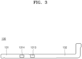
- FIGS. 2 and 3 respectively show one side and another side of a protection circuit module 130 according to one or more embodiments
- FIG. 4 shows a front view of a portion of the battery pack 10 according to one or more embodiments
- FIG. 5 shows a cross-sectional view of the battery pack 10 according to one or more embodiments.
- the battery pack 10 includes an electrode assembly 110, a case 120, a protection circuit module 130, a fixing bracket (e.g., a fixing member) 140, and a heat dissipator (e.g., a heat dissipation member) 150.
- a fixing bracket e.g., a fixing member
- a heat dissipator e.g., a heat dissipation member
- the electrode assembly 110 may be manufactured in a jelly roll form by winding a separator 113 arranged between a first electrode plate 111 and a second electrode plate 112. Alternatively, the electrode assembly 110 may be manufactured in a stack form by stacking separators 113 between a plurality of first electrode plates 111 and a plurality of second electrode plates 112. Alternatively, the electrode assembly 110 may be manufactured by applying both a jelly roll and a stack.
- the first electrode plate 111 includes a first active material coating portion formed by intermittently coating a first active material on a first substrate, which is a sheet-form conductive material, and a first non-coating portion, which is a portion where the first substrate is exposed without being coated with the first active material.
- the first electrode plate 111 may be a negative electrode plate, and the first active material may be a negative active material including a carbon material, such as crystalline carbon, amorphous carbon, carbon composite, carbon fiber, or the like, lithium metal, or a lithium alloy.
- the second electrode plate 112 includes a second active material coating portion including a polarity that is different from that of the first electrode plate 111.
- the second electrode plate 112 is formed by intermittently coating a second active material on a second substrate, which is a sheet-form conductive material, and a second non-coating portion, which is a portion where the second substrate is exposed without being coated with the second active material.
- the second electrode plate 112 may be a positive electrode plate, and the second active material may include a positive electrode active material including lithium, such as LiCoO 2 , LiNiO 2 , LiMnO 2 , LiMn 2 O 4 , LiNi 1-x-y Co x M y O 2 , and/or the like.
- the separator 113 is between the first electrode plate 111 and the second electrode plate 112.
- the separator 113 may insulate the first electrode plate 111 and the second electrode plate 112, and may exchange lithium ions between the first electrode plate 111 and the second electrode plate 112.
- the separator 113 may have a sufficient length to completely insulate the first electrode plate 111 from the second electrode plate 112 even when the electrode assembly 110 shrinks or expands in a process of charging/discharging the battery pack 10.
- Electrode tabs 114 may be respectively arranged on the first electrode plate 111 and the second electrode plate 112 to protrude to one side.
- two electrode tabs 114 may be provided to respectively correspond to the first electrode plate 111 and the second electrode plate 112.
- one electrode tab 114 may be electrically connected to one side of the first non-coating portion of the first electrode plate 111 to extend toward the outside of the electrode assembly 110.
- another electrode tab 114 may be electrically connected to one side of the second non-coating portion of the second electrode plate 112 to extend toward the outside of the electrode assembly 110.
- a film portion 115 may be arranged on the electrode tab 114.
- the film portion 115 is arranged on one surface of the electrode tab 114, or is arranged to surround (e.g., partially surround) the electrode tab 114.
- the film portion 115 may seal the electrode tab 114 exposed to the outside of the electrode assembly 110.
- the film portion 115 is thermally fused with the sealing portion 124 to cause the electrode tab 114 and the sealing portion 124 to be closely coupled to each other.
- the case 120 forms an exterior of the battery pack 10, and the electrode assembly 110 is arranged in the case 120.
- the shape and size of the case 120 are not particularly limited, and may have a shape and size corresponding to the shape and size of the electrode assembly 110.
- the case 120 may have a rectangular parallelepiped shape with an empty interior.
- the case 120 may have a polyhedral shape of another shape, or may have a cylindrical shape.
- the case 120 may include a cover 121, a lower case 122, an inner space 123, and the sealing portion 124.
- the lower case 122 includes the inner space 123 having a greater size than that of the electrode assembly 110, and the electrode assembly 110 is inserted into the inner space 123.
- the cover 121 is arranged on an upper surface of the lower case 122 such that it is able to be open and closed, so that the electrode assembly 110 is covered when being inserted into the inner space 123.
- the sealing portion 124 is arranged along an upper edge of the lower case 122. As shown in FIG. 1 , in a state where the electrode assembly 110 is accommodated inside the case 120, a portion of the electrode tab 114 is exposed to the outside of the case 120.
- the film portion 115 provided on the electrode tab 114 may be between the cover 121 and the lower case 122 at a position corresponding to the sealing portion 124.
- the protection circuit module 130 includes electric circuits and various types of elements for reducing or preventing the likelihood of overcharge, overdischarge, overcurrent, and for reducing or preventing the likelihood of short circuit of the battery pack 10, for example, of the electrode assembly 110.
- the protection circuit module 130 is arranged outside the case 120, and is connected to the electrode tab 114.
- the protection circuit module 130 is arranged below the electrode tab 114, which may correspond to a cell terrace portion of the battery pack 10.
- the protection circuit module 130 includes a substrate 131 and a connector 132.
- the substrate 131 includes electronic components and circuits for reducing or preventing the likelihood of overdischarge, overcharge, and overcurrent of the battery pack 10, and may be a flexible printed circuit board (FPCB).
- the connector 132 may be connected to the substrate 131 to connect the protection circuit module 130 to an external device.
- a plurality of field effect transistors (FET) 1311, 1312, 1313, and 1314 may be arranged on the substrate 131.
- FET field effect transistors
- two FETs 1311 and 1312 may be arranged on an upper surface of the substrate 131
- two FETs 1313 and 1314 may be arranged on a lower surface of the substrate 131.
- These FETs 1311, 1312, 1313, and 1314 control a protection circuit provided on the substrate 131.
- the connector 132 extends from one side of the substrate 131 to have a bent end portion.
- a connection terminal 1321 may be arranged at a distal end portion of the connector 132 to electrically connect the protection circuit module 130 and an external device to each other.
- the fixing bracket 140 is mounted on the outside of the case 120 to cover the protection circuit module 130.
- the fixing bracket 140 may be mounted to cover the upper and lower surfaces of the protection circuit module 130.
- the fixing bracket 140 may protect the protection circuit module 130 from external impact while stably fixing the protection circuit module 130 to the electrode tab 114.
- the fixing bracket 140 may have, substantially, a "C" shape (e.g., a bracket shape, "[" shape, or a three-sided, three-dimensional object) to surround or abut at least the upper surface, a side surface, and/or the lower surface of the protection circuit module 130.
- the fixing bracket 140 may include a first fixing surface 141 inserted from the outside of the protection circuit module 130 for covering the upper surface of the protection circuit module 130, a second fixing surface 142 covering a side surface of the protection circuit module 130, and a third fixing surface 143 covering the lower surface of the protection circuit module 130.
- the first fixing surface 141 may be arranged to correspond to the upper surface of the protection circuit module 130, and may contact the FETs 1311 and 1312.
- the second fixing surface 142 may be bent downward from an end portion of the first fixing surface 141 to contact a side surface (e.g., a left side surface in FIG. 5 ) of the substrate 131.
- the third fixing surface 143 may be bent toward the case 120 from an end portion of the second fixing surface 142, and may be arranged to correspond to the lower surface of the substrate 131 to contact the FETs 1313 and 1314.
- An inner side end portion (e.g., a right-side end portion in FIG. 5 ) of the fixing bracket 140 may be fixed to the case 120.
- the fixing bracket 140 may be fixing tape.
- the fixing bracket 140 may include an adhesive material on at least the first fixing surface 141, the second fixing surface 142, and/or the third fixing surface 143 to be fixed to the protection circuit module 130.
- the heat dissipator 150 is arranged outside of (e.g., at an exterior of, or partially surrounding) the fixing bracket 140 to discharge heat generated by the battery pack 10 to the outside.
- the heat dissipator 150 may be arranged to surround, or abut, an upper surface, a side surface, and a lower surface of the fixing bracket 140.
- the heat dissipator 150 may be arranged to surround the protection circuit module 130.
- the heat dissipator 150 may be arranged to overlap at least the FETs 1311, 1312, 1313, and/or 1314 arranged on the substrate 131 in a state of being arranged outside the fixing bracket 140. Accordingly, the heat dissipator 150 may discharge heat emitted by the FETs 1311, 1312, 1313, and 1314 to the outside of the battery pack 10.
- the heat dissipator 150 may be a heat dissipation tape. Portions of the heat dissipator 150 may be respectively attached to the outside of the upper surface, the side surface, and/or the lower surface of the fixing bracket 140.
- the sum of areas of the portions of the heat dissipator 150 may be greater than the sum of areas of the plurality of FETs 1311, 1312, 1313, and 1314.
- the heat dissipator 150 may have, substantially, a "C" shape (e.g., a three-sided, three-dimensional object) to surround at least the upper surface, the side surface, and/or the lower surface of the fixing bracket 140.
- the heat dissipator 150 may include a first heat dissipation surface 151 inserted from the outside of the fixing bracket 140 and covering the upper surface of the fixing bracket 140, a second heat dissipation surface 152 covering the side surface of the fixing bracket 140, and a third heat dissipation surface 153 covering the lower surface of the fixing bracket 140.
- the first heat dissipation surface 151 may be arranged to correspond to the first fixing surface 141 of the fixing bracket 140. As shown in FIGS. 1 , 4 , and 5 , the first heat dissipation surface 151 may be arranged outside the first fixing surface 141, and may have a smaller area than that of the first fixing surface 141. The first heat dissipation surface 151 may have a greater area than the sum of areas of the FETs 1311 and 1312 arranged on the upper surface of the substrate 131.
- the FETs 1311 and 1312 may be arranged inside (e.g., at an interior of) the first heat dissipation surface 151 (e.g., may be overlapped by, or entirely overlapped by, the first heat dissipation surface 151). Accordingly, the first heat dissipation surface 151 may absorb heat that is generated by the substrate 131, for example, generated by the FETs 1311 and 1312 arranged on the upper surface of the substrate 131, and that is transferred to the first fixing surface 141 of the fixing bracket 140, to efficiently discharge the heat to the outside of the battery pack 10.
- the second heat dissipation surface 152 may be arranged to correspond to the second fixing surface 142 of the fixing bracket 140. As shown in FIGS. 1 , 4 , and 5 , the second heat dissipation surface 152 may be arranged outside the second fixing surface 142, and may have a smaller area than that of the second fixing surface 142. The second heat dissipation surface 152 may extend downward from an end portion of the first heat dissipation surface 151, and may be arranged to cover, or overlap, the FETs 1311, 1312, 1313, and 1314 respectively arranged on an upper portion and a lower portion of the substrate 131. Accordingly, heat that is generated by the FETs 1311, 1312, 1313, and 1314, and that is transferred to the second fixing surface 142 of the fixing bracket 140, may be absorbed to be efficiently discharged to the outside of the battery pack 10.
- the third heat dissipation surface 153 may be arranged to correspond to the third fixing surface 143 of the fixing bracket 140. As shown in FIGS. 1 , 4 , and 5 , the third heat dissipation surface 153 may be arranged below the third fixing surface 143, and may have a smaller area than that of the third fixing surface 143. The third heat dissipation surface 153 may extend toward the case 120 from an end portion of the second heat dissipation surface 152, and may be arranged to cover the FETs 1313 and 1314 arranged on the lower portion of the substrate 131.
- the third heat dissipation surface 153 may have a greater area than the sum of areas of the FETs 1313 and 1314 arranged on the lower surface of the substrate 131. Also, the FETs 1313 and 1314 may be arranged inside the third heat dissipation surface 153. Accordingly, the third heat dissipation surface 153 may absorb heat that is generated by the substrate 131, for example, generated by the FETs 1313 and 1314 arranged on the lower surface of the substrate 131, and that is transferred to the third fixing surface 143 of the fixing bracket 140, to efficiently discharge the heat to the outside of the battery pack 10.
- the heat dissipator 150 further includes a heat dissipation element 154.
- the heat dissipation element 154 may be arranged on one side of the heat dissipator 150 to absorb heat generated by the protection circuit module 130 to discharge the heat to the outside of the battery pack 10.
- one or more heat dissipation elements 154 may be arranged on an inner side surface of the heat dissipator 150 to be positioned between the fixing bracket 140 and the heat dissipator 150.
- the heat dissipation element 154 may include a material having higher thermal conductivity than that of the fixing bracket 140 and the heat dissipator 150.
- the heat dissipation element 154 may be a metal layer, and, for example, may be a thin film including aluminium.
- the heat dissipation element 154 may be detachably arranged on the heat dissipator 150.
- one heat dissipation element 154 may be arranged inside the first heat dissipation surface 151 of the heat dissipator 150, and one heat dissipation element 154 may be arranged inside the third heat dissipation surface 153 of the heat dissipator 150. As shown in FIGS. 4 and 5 , the heat dissipation element 154 may be arranged inside the first heat dissipation surface 151 to contact an upper surface of the first fixing surface 141. Also, the heat dissipation element 154 may be arranged inside the third heat dissipation surface 153 to contact a lower surface of the third fixing surface 143. Accordingly, heat generated by the FETs 1311, 1312, 1313, and 1314 may be respectively arranged on the upper surface and lower surface of the substrate 131 to efficiently discharge the heat to the outside of the battery pack 10.
- the heat dissipation elements 154 may be symmetrically arranged with the substrate 131 therebetween. As shown in FIGS. 4 and 5 , the heat dissipation elements 154 may be respectively arranged to correspond to the upper surface and the lower surface of the substrate 131 and may be arranged to overlap each other.
- the heat dissipation element 154 may have a greater area than the areas of the FETs 1311, 1312, 1313, and 1314.
- an area of the heat dissipation element 154 arranged on the first heat dissipation surface 151 may be greater than the sum of areas of the FETs 1311 and 1312 arranged on the upper surface of the substrate 131.
- the FETs 1311 and 1312 may be arranged inside the first heat dissipation surface 151.
- an area of the heat dissipation element 154 arranged on the third heat dissipation surface 153 may be greater than the sum of areas of the FETs 1313 and 1314 arranged on the lower surface of the substrate 131. Accordingly, heat generated by the FETs 1311, 1312, 1313, and 1314 may be stably discharged to the outside of the battery pack 10 through the heat dissipation element(s) 154 without being transferred to the battery pack 10.
- the heat dissipation element 154 in a state where the first heat dissipation surface 151 and the third heat dissipation surface 153 are arranged outside the fixing bracket 140, the heat dissipation element 154 may be inserted therebetween.
- the heat dissipation element 154 may have a smaller area than that of the first heat dissipation surface 151 and the third heat dissipation surface 153. Accordingly, both ends of the first heat dissipation surface 151 contact one surface of the first fixing surface 141, and both ends of the third heat dissipation surface 153 contact one surface of the third fixing surface 143.
- first heat dissipation surface 151 and the third heat dissipation surface 153 may each have a shape surrounding the heat dissipation element 154, and a heat insulation space 155 may be partitioned by the first to third heat dissipation surfaces 151 to 153, the heat dissipation element 154, and the fixing bracket 140.
- the heat insulation space 155 may perform an insulation function so that heat transferred from the FETs 1311, 1312, 1313, and 1314 is not transferred to the battery pack 10.
- the battery pack 10 may efficiently discharge heat generated by the protection circuit module 130, for example, generated by the FETs 1311, 1312, 1313, and 1314, to the outside of the battery pack 10 through the heat dissipation element 154.
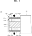
- FIG. 6 shows a cross-sectional view of a battery pack 10A according to one or more other embodiments.
- the battery pack 10A may include a different heat dissipator 150A compared to the battery pack 10 according to the above-described embodiments.
- Other configurations of the battery pack 10A may be the same as those of the battery pack 10, and detailed descriptions thereof are omitted.
- the battery pack 10A includes the heat dissipator 150A.
- the heat dissipator 150A may include a first heat dissipation surface 151A, a second heat dissipation surface 152A, and a third heat dissipation surface 153A, which are arranged outside the fixing bracket 140 and the first to third fixing surfaces 141A to 143A, and are positioned to respectively correspond to a first fixing surface 141A, a second fixing surface 142A, and a third fixing surface 143A of the fixing bracket 140A.
- the battery pack 10A includes a heat dissipation element 154A.
- the heat dissipation element 154A may be integrally formed with the heat dissipator 150A. That is, unlike the heat dissipation element 154 according to the embodiments described above, which is additionally arranged inside each of the first heat dissipation surface 151 and the third heat dissipation surface 153, the heat dissipation element 154A according to one or more embodiments may be integrally formed with the heat dissipator 150A to replace a partial area of (e.g., to be coplanar with) the heat dissipator 150A, for example, a partial area(s) of the first heat dissipation surface 151A and/or the third heat dissipation surface 153A. Accordingly, the heat dissipator 150A may be arranged in closer contact with the fixing bracket 140 without a gap.
- the heat dissipation element 154A is integrally formed with the first heat dissipation surface 151A and the third heat dissipation surface 153A, entire surfaces of the first heat dissipation surface 151A and the third heat dissipation surface 153A, each including the heat dissipation element 154A, may be in close contact with the fixing bracket 140. Accordingly, the heat dissipator 150A may be more firmly fixed to the fixing bracket 140, and heat transferred to the fixing bracket 140 may be transferred to the heat dissipator 150A without loss.
- both surfaces of the heat dissipation element 154A may include a transparent material.
- a lower surface of the heat dissipation element 154A, which faces the fixing bracket 140, and an upper surface corresponding to the lower surface may all include a transparent material.
- the heat dissipation element 154A may include one surface including a transparent material, and another surface including an opaque material.
- the heat dissipation element 154A may include a lower surface including a transparent material, and an upper surface including an opaque material.
- the heat dissipation element 154A may include an upper surface including a transparent material and a lower surface including an opaque material.
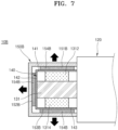
- FIG. 7 shows a cross-sectional view of a battery pack 10B according to one or more other embodiments.
- the battery pack 10B includes a different heat dissipator 150B compared to the battery pack 10 according to the above-described embodiments.
- Other configurations of the battery pack 10B may be the same as those of the battery pack 10, and detailed descriptions thereof are omitted.
- the battery pack 10B includes the heat dissipator 150B.
- the heat dissipator 150B may include a first heat dissipation surface 151B, a second heat dissipation surface 152B, and a third heat dissipation surface 153B, which are arranged outside the fixing bracket 140 and are positioned to respectively correspond to the first fixing surface 141, the second fixing surface 142, and the third fixing surface 143 of the fixing bracket 140.
- the battery pack 10B includes a heat dissipation element 154B. As shown in FIG. 7 , the heat dissipation element 154B may be arranged inside each of the first heat dissipation surface 151B, the second heat dissipation surface 152B, and the third heat dissipation surface 153B.
- the heat dissipation element 154B may be additionally arranged inside (e.g., at an interior of) the second heat dissipation surface 152B. Accordingly, heat generated by side surfaces of the protection circuit module 130 may not flow into the battery pack 10B and may be discharged to the outside of the battery pack 10B through the heat dissipation element 154B arranged on the second heat dissipation surface 152B.
- a battery pack includes a heat dissipation structure, so that heat generated by a protection circuit module, for example, by an FET, may be discharged to the outside with being transferred to the battery pack.
- a protection circuit module for example, by an FET
- a battery pack according to one or more embodiments may implement a compact heat dissipation structure without increasing, or without substantially increasing, the size of the battery pack through a thin film heat dissipator.
- a battery pack according to one or more embodiments may efficiently discharge heat generated by an FET by arranging a heat dissipation element to correspond to the FET.
Landscapes
- Chemical & Material Sciences (AREA)
- Chemical Kinetics & Catalysis (AREA)
- Electrochemistry (AREA)
- General Chemical & Material Sciences (AREA)
- Engineering & Computer Science (AREA)
- Manufacturing & Machinery (AREA)
- Microelectronics & Electronic Packaging (AREA)
- Battery Mounting, Suspending (AREA)
- Secondary Cells (AREA)
Applications Claiming Priority (1)
| Application Number | Priority Date | Filing Date | Title |
|---|---|---|---|
| KR1020220116635A KR102917726B1 (ko) | 2022-09-15 | 2022-09-15 | 방열 구조를 포함하는 배터리 팩 |
Publications (2)
| Publication Number | Publication Date |
|---|---|
| EP4354570A2 true EP4354570A2 (de) | 2024-04-17 |
| EP4354570A3 EP4354570A3 (de) | 2024-07-10 |
Family
ID=87863401
Family Applications (1)
| Application Number | Title | Priority Date | Filing Date |
|---|---|---|---|
| EP23194378.8A Pending EP4354570A3 (de) | 2022-09-15 | 2023-08-30 | Batteriepack mit wärmeableitungsstruktur |
Country Status (4)
| Country | Link |
|---|---|
| US (1) | US20240097213A1 (de) |
| EP (1) | EP4354570A3 (de) |
| KR (1) | KR102917726B1 (de) |
| CN (1) | CN117712061A (de) |
Cited By (1)
| Publication number | Priority date | Publication date | Assignee | Title |
|---|---|---|---|---|
| EP4618229A1 (de) * | 2024-03-12 | 2025-09-17 | Samsung Sdi Co., Ltd. | Batteriepack |
Family Cites Families (7)
| Publication number | Priority date | Publication date | Assignee | Title |
|---|---|---|---|---|
| KR100947963B1 (ko) * | 2007-09-28 | 2010-03-15 | 삼성에스디아이 주식회사 | 이차 전지용 보호회로 기판과 이를 이용한 이차 전지 |
| JP2015088380A (ja) * | 2013-10-31 | 2015-05-07 | 日立マクセル株式会社 | 電池パック |
| KR102362074B1 (ko) * | 2017-03-10 | 2022-02-11 | 삼성전자주식회사 | 방열 플레이트를 포함하는 배터리 및 이를 포함하는 전자 장치 |
| KR102221780B1 (ko) * | 2017-05-04 | 2021-03-02 | 주식회사 엘지화학 | 배터리 팩 및 이의 제조방법 |
| KR102179687B1 (ko) * | 2017-05-29 | 2020-11-17 | 주식회사 엘지화학 | 배터리 팩 및 이의 제조방법 |
| US11190029B2 (en) * | 2019-05-15 | 2021-11-30 | Semiconductor Components Industries, Llc | Methods and apparatus for a battery |
| KR102755060B1 (ko) * | 2020-10-29 | 2025-01-20 | 주식회사 엘지에너지솔루션 | 방열 테이프를 이용한 보호회로 모듈 방열 구조를 포함하는 전지팩 |
-
2022
- 2022-09-15 KR KR1020220116635A patent/KR102917726B1/ko active Active
-
2023
- 2023-08-22 US US18/453,827 patent/US20240097213A1/en active Pending
- 2023-08-30 EP EP23194378.8A patent/EP4354570A3/de active Pending
- 2023-09-14 CN CN202311192114.6A patent/CN117712061A/zh active Pending
Cited By (1)
| Publication number | Priority date | Publication date | Assignee | Title |
|---|---|---|---|---|
| EP4618229A1 (de) * | 2024-03-12 | 2025-09-17 | Samsung Sdi Co., Ltd. | Batteriepack |
Also Published As
| Publication number | Publication date |
|---|---|
| CN117712061A (zh) | 2024-03-15 |
| US20240097213A1 (en) | 2024-03-21 |
| EP4354570A3 (de) | 2024-07-10 |
| KR102917726B1 (ko) | 2026-01-23 |
| KR20240037740A (ko) | 2024-03-22 |
Similar Documents
| Publication | Publication Date | Title |
|---|---|---|
| CN111682250B (zh) | 二次电池 | |
| US8518575B2 (en) | Pouch-type lithium secondary battery and fabrication method thereof | |
| CN100461524C (zh) | 胶状卷绕型电极组件和具有该电极组件的锂二次电池 | |
| CN113991231B (zh) | 电池组 | |
| CN109428043B (zh) | 二次电池 | |
| US20230231283A1 (en) | Secondary battery | |
| US8785021B2 (en) | Battery pack | |
| US20150380715A1 (en) | Secondary battery | |
| CN106356475A (zh) | 二次电池 | |
| WO2019017637A1 (ko) | 이차전지용 파우치 외장재, 이를 이용한 파우치형 이차전지 및 그 제조 방법 | |
| KR20170002140A (ko) | 이차 전지 및 그 제조 방법 | |
| CN111755731A (zh) | 二次电池 | |
| EP4354570A2 (de) | Batteriepack mit wärmeableitungsstruktur | |
| US8465870B2 (en) | Secondary battery with improved capacity and installation convenience | |
| CN102136563A (zh) | 电极组件及其制造方法和包括电极组件的二次电池 | |
| KR101797694B1 (ko) | 보호회로 모듈을 포함하는 전지팩 | |
| US11075433B2 (en) | Rechargeable battery including an overcharge safety device | |
| KR100362277B1 (ko) | 보호 케이스를 가지는 이차 전지 | |
| US20250192388A1 (en) | Secondary battery | |
| KR101763265B1 (ko) | 계단 구조의 전극조립체에 대응하는 트리밍부가 형성되어 있는 전지케이스를 포함하는 전지셀 | |
| US12476331B2 (en) | Battery module and battery pack including the same | |
| KR20040107868A (ko) | 파우치형 리튬 이차 전지 | |
| CN116505149A (zh) | 二次电池及二次电池的制造方法 | |
| US8765299B2 (en) | Electrode assembly and secondary battery including the same | |
| CN106469830A (zh) | 二次电池及其制造方法 |
Legal Events
| Date | Code | Title | Description |
|---|---|---|---|
| PUAI | Public reference made under article 153(3) epc to a published international application that has entered the european phase |
Free format text: ORIGINAL CODE: 0009012 |
|
| STAA | Information on the status of an ep patent application or granted ep patent |
Free format text: STATUS: REQUEST FOR EXAMINATION WAS MADE |
|
| 17P | Request for examination filed |
Effective date: 20230830 |
|
| AK | Designated contracting states |
Kind code of ref document: A2 Designated state(s): AL AT BE BG CH CY CZ DE DK EE ES FI FR GB GR HR HU IE IS IT LI LT LU LV MC ME MK MT NL NO PL PT RO RS SE SI SK SM TR |
|
| PUAL | Search report despatched |
Free format text: ORIGINAL CODE: 0009013 |
|
| AK | Designated contracting states |
Kind code of ref document: A3 Designated state(s): AL AT BE BG CH CY CZ DE DK EE ES FI FR GB GR HR HU IE IS IT LI LT LU LV MC ME MK MT NL NO PL PT RO RS SE SI SK SM TR |
|
| RIC1 | Information provided on ipc code assigned before grant |
Ipc: H01M 50/287 20210101ALI20240604BHEP Ipc: H01M 50/271 20210101ALI20240604BHEP Ipc: H01M 10/6553 20140101ALI20240604BHEP Ipc: H01M 10/6551 20140101ALI20240604BHEP Ipc: H01M 10/647 20140101ALI20240604BHEP Ipc: H01M 10/613 20140101ALI20240604BHEP Ipc: H01M 10/04 20060101AFI20240604BHEP |