EP4354352A1 - Neuromorphe schaltung - Google Patents
Neuromorphe schaltung Download PDFInfo
- Publication number
- EP4354352A1 EP4354352A1 EP23203111.2A EP23203111A EP4354352A1 EP 4354352 A1 EP4354352 A1 EP 4354352A1 EP 23203111 A EP23203111 A EP 23203111A EP 4354352 A1 EP4354352 A1 EP 4354352A1
- Authority
- EP
- European Patent Office
- Prior art keywords
- voltage
- output
- neural
- neural circuit
- conductive line
- Prior art date
- Legal status (The legal status is an assumption and is not a legal conclusion. Google has not performed a legal analysis and makes no representation as to the accuracy of the status listed.)
- Pending
Links
Images




Classifications
-
- G—PHYSICS
- G06—COMPUTING OR CALCULATING; COUNTING
- G06N—COMPUTING ARRANGEMENTS BASED ON SPECIFIC COMPUTATIONAL MODELS
- G06N3/00—Computing arrangements based on biological models
- G06N3/02—Neural networks
- G06N3/06—Physical realisation, i.e. hardware implementation of neural networks, neurons or parts of neurons
- G06N3/063—Physical realisation, i.e. hardware implementation of neural networks, neurons or parts of neurons using electronic means
- G06N3/065—Analogue means
Definitions
- the present description generally relates to a neuromorphic circuit and, more particularly, to a neuromorphic circuit implemented using a resistive random access memory (RRAM).
- RRAM resistive random access memory
- Neuromorphic circuits have been proposed to reproduce the main characteristics of a biological neuron. Such circuits are configured to integrate signals, originating from other neuromorphic circuits, over time.
- CMOS Complementary Metal Oxide Semiconductor
- SRAM Static random access memory
- RRAM resistive random access memory
- Large capacitors are used to implement dynamic neurons, equivalent to the membrane potential of a biological neuron.
- digital solutions can be used, sampling signals and copying them to external memory.
- Embodiments of the present description overcome all or part of the disadvantages of known neural circuits.
- the output device is a voltage comparator configured to generate a transition of the output voltage of the neural circuit when the first voltage exceeds the threshold voltage.
- the output device is a voltage amplifier configured to generate an analog output voltage.
- the neural circuit further comprises a first delay circuit connected to an output of the voltage comparator and configured to reset the first voltage on the first common conductive line in response to the transition of the output voltage.
- the first delay circuit is configured to propagate with a delay the transition of the output voltage and to thus cause the complete discharge of each of the parasitic capacitances when the first voltage becomes greater than the threshold voltage.
- the first resistive element of each synapse is connected to an output of an additional corresponding neuronal circuit.
- the first resistive element of each synapse is connected to a supply voltage via a first corresponding transistor, each of the first transistors having its gate connected to an output of an additional corresponding neuronal circuit .
- each synapse further comprises a second resistive memory element having an associated parasitic capacitance, each of the second resistive memory elements being configured to supply a current to a second common conductive line, the second conductive line supplying the threshold voltage to the output device.
- the second resistive element of each synapse is connected to the output of the additional corresponding neuronal circuit.
- the second resistive element of each synapse is connected to the supply voltage via a second corresponding transistor, each of the second transistors having its gate connected to an output of the additional corresponding neuronal circuit.
- the neural circuit further comprises a second delay circuit connected to the output of the voltage comparator and configured to reset the threshold voltage on the second common conductive line in response to the transition of the output voltage.
- the first resistive memory elements are ferro-tunnel junction elements.
- the parasitic capacitance associated with each resistive memory element is located only in the synapse.
- the output device comprises a transistor configured to discharge the associated parasitic capacitance when the first voltage becomes greater than the threshold voltage.
- a neural network comprising a plurality of layers of neural circuits as described above.
- transistors are described as having main conduction nodes and a gate node, without limitation to any particular transistor technology.
- the main conduction nodes are the source and the drain.
- MOS transistors are N-channel devices, although those skilled in the art will know how to adapt the embodiments to the case of P-channel MOS transistors. It would also be possible to use other transistor technologies.
- the main conduction nodes are the collector and emitter and the gate is implemented by the base.
- the expressions “approximately”, “approximately”, “substantially”, and “of the order of” mean to the nearest 10%, preferably to the nearest 5%.
- FIG 1 schematically represents a hardware implementation of a neural pulse circuit based on CMOS 100 according to an embodiment which has been proposed.
- the neural circuit 100 is part of a network neuronal (not shown in figure 1 ) comprising a plurality of neural circuits similar to circuit 100.
- the neural circuit 100 includes three stages.
- a first stage 102 includes, for example, a resistive random access memory matrix (RRAM).
- the matrix RR_AM 102 includes a number N + 1 of programmable resistive elements G 0 to G N implementing the synapses of the neuronal circuit 100.
- Each resistive element G i , i ⁇ ⁇ 0,..., N ⁇ has for example a first electrode, for example its lower electrode, connected to a supply voltage rail at a voltage V bot via a corresponding transistor T i .
- Each transistor T i , i E ⁇ 0,...,N ⁇ has its gate connected to receive a corresponding voltage V in,i , i ⁇ ⁇ 0 , ...,N ⁇ supplied by another neural circuit of the neural network or by an input node of the neural network.
- Each resistive element G i , i ⁇ ⁇ 0, ..., N ⁇ has for example a second electrode, for example its upper electrode, connected to a common conductive line SL.
- the RRAM matrix 102 is made up of N + 1 branches connected between the conductive line SL and the supply voltage rail V bot , each branch comprising the series connection of a resistive element G i , i ⁇ ⁇ 0, ..., N ⁇ and a transistor T i .
- a second stage 104 of the neural circuit 100 is a current replication circuit having an analog CMOS implementation and configured to generate a current on its output line 105 which is equal to or proportional to the sum of the currents passing through the N + 1 branches of the RR_AM matrix 102.
- the current replication circuit 104 comprises a transistor M 1 connected by its main conduction nodes between a supply voltage rail at a voltage Vdd and the conductive line SL and a transistor M 2 connected by its main conduction nodes between the rail of supply voltage Vdd and the output line 105.
- the supply voltage Vdd is for example greater than the supply voltage V bot .
- the current replication circuit 104 further comprises an operational amplifier 106 having a positive input connected to the conductive line SL, a negative input connected to a threshold voltage V th and its output connected to the gates of the transistors M 1 and M 2 .
- the threshold voltage V th is an intermediate voltage between the voltages V bot and Vdd and the operational amplifier 106 is for example configured to adjust the gate voltage of the transistors M 1 and M 2 so that the voltage on the conductive line SL is equal to the threshold voltage V th .
- the transistor M 2 conducts a current I out equal to or proportional to the current in the transistor M 1 .
- the current replication circuit 104 further comprises a transistor M 3 connected in series to the transistor M 2 , having for example its main conduction nodes connected respectively to the output line 105 and to ground (GND).
- the gate of transistor M 3 is for example connected to output line 105, which supplies a current to the third stage 108.
- the current supplied by output line 105 charges a capacitor (not shown) of the third stage 108.
- a third stage 108 comprises, for example, a synapse 110 (DPI SYNAPSE) with a differential pair integrator (DPI) and a leaky integrate-and-fire (LIF) neuron 112.
- DPI SYNAPSE differential pair integrator
- LIF leaky integrate-and-fire
- the DPI synapse 110 receives, for example, the output signal from the current replication circuit 104 and performs an integration of this signal.
- the LIF neuron 112 receives, for example, the integrated signal coming from the DPI synapse 110 and generates an output voltage V out having a pulse when the integrated signal exceeds a threshold.
- a problem with the neural circuit 100 of the figure 1 is that relatively high capacities are present in the DPI synapse 110 and the LIF neuron 112, leading to relatively large energy consumption and surface area. This is a serious problem when the complexity of the neural network increases, involving a relatively large number of neurons.
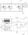
- FIG. 2 schematically represents a neural circuit based on RRAM 200 according to an exemplary embodiment of the present description.
- the neural circuit 200 includes an input stage 202 and an output stage 204.
- the input stage 202 includes for example a resistive random access memory matrix (RRAM).
- RRAM resistive random access memory matrix
- the RRAM matrix 202 comprises a number N + 1 of programmable resistive elements G 0 to G N implementing the synapses of the neuronal circuit 100.
- each resistive element G i , i ⁇ ⁇ 0, ..., N] has for example one of its electrodes, for example its upper electrode, connected to a common conductive line SL.
- Each resistive element G i , i ⁇ ⁇ 0, ..., N ⁇ of the memory matrix 202 has for example a first electrode, for example its lower electrode, connected to a supply voltage rail V bot via of a corresponding transistor T i .
- Each transistor T i , i ⁇ ⁇ 0, ..., N ⁇ has for example its gate connected to receive a corresponding voltage V in,i , i ⁇ ⁇ 0, ... , N ⁇ supplied by another neural circuit of the neural network or by an input node of the neural network.
- the RRAM matrix 202 is made up of N + 1 branches connected between the conductive line SL and the supply voltage rail V bot , each branch comprising the connection in series of a resistive element G i , i ⁇ ⁇ 0, ... , N ⁇ , with its associated capacitance C i , and a corresponding transistor T;.
- V i ( s ) is the individual voltage which is applied between the electrodes of the resistive element G i at a time s
- G i is the conductivity of the resistive element G i .
- the voltage V i ( s ) depends on the voltages V bot and V in,i .
- Each resistive element G i , i ⁇ ⁇ 0, ..., N ⁇ has a parasitic capacitance C i , i ⁇ ⁇ 0, ...,N ⁇ , corresponding to the low capacitance effect of each resistive element.
- the type of memory of the resistive element G i is for example chosen so that the parasitic capacitances C i are relatively high, which leads to a relatively high capacitance at the level of the common conductive line SL.
- each resistive element G i , i ⁇ ⁇ 0, ..., N ⁇ is implemented by a ferro-tunnel junction element.
- Ferro-tunnel junction elements are well known to those skilled in the art and are for example described in more detail in the publication " Low-power linear computation using nonlinear ferroelectric tunnel junction memristors” published in “Nature Electronics 3.5 (2020)” by Berdan, Roh , et al. According to a variant, it would be possible to use other types of resistive memory elements, in particular, those having relatively high parasitic capacitances, such as, for example, ferroelectric field effect transistors (FeFET) or devices High resistance OxRAM.
- FeFET ferroelectric field effect transistors
- OxRAM High resistance OxRAM
- the output stage 204 of the neural circuit 200 comprises for example a comparator 206 having a positive input connected to the common conductive line SL and a negative input connected to a threshold voltage V th .
- the comparator 206 is for example configured to compare the voltage on the common conductive line SL to the threshold voltage V th and to generate a transition of an output voltage V out of the neural circuit 200 when the voltage on the common conductive line SL exceeds the threshold voltage V th .
- the capacitive effect of the resistive elements G i of the memory matrix 202 replaces capacitors to be integrated into the DPI synapse and/or the LIF neural circuits of stage 108 of the figure 1 .
- the common conductive line SL is charged by the sum of the currents passing through each of the N+1 branches of the input stage 202 and the comparator 206 is used to detect the moment at which the voltage on the conductive line common SL exceeds the threshold voltage V th and to generate a corresponding output transition in the output voltage V out .
- FIG. 3 schematically represents a neural circuit based on RRAM 300 according to another embodiment of the present description.
- the neural circuit 300 is similar to the neural circuit 200 of the figure 2 and includes the same output stage 204, but includes an input stage 302 instead of the input stage 202.
- the input stage 302 is similar to the input stage 202 in that it comprises N+1 branches each comprising a resistive element G i , i ⁇ ⁇ 0,..., N ⁇ including one of the electrodes , for example its upper electrode, is connected to the common conductive line SL.
- the other electrode of each resistive element G i , i ⁇ ⁇ 0 , ... , N ⁇ which is for example its lower electrode, is connected directly to the corresponding voltage V in,i , i E ⁇ 0, ... , N ⁇ supplied by another neural circuit of the neural network or by an input node of the neural network.
- transistors T described in relation to the figure 2 are omitted in the embodiment of the Figure 3 .
- the operation of the neural circuit 300 of the Figure 3 is similar to that of the neural circuit 200 of the figure 2 , except that the voltage applied to each resistive element G i , i ⁇ ⁇ 0, ..., N ⁇ is no longer a function of the supply voltage V bot , but only of the input voltage corresponding V in,i , i ⁇ ⁇ 0 , ..., N ⁇ .
- FIG 4 represents an example of a ferro-tunnel junction (FTJ) element 400 and its equivalent circuit 400'.
- the FTJ element 400 is for example used to implement the resistive elements G i in the neural circuits 200 and 300 of the figures 2 And 3 .
- the FTJ element 400 is for example made up of a stack of layers comprising a lower electrode 402 (BE), a layer of silicon dioxide 404 (SiO 2 ) formed in the lower electrode 402, a layer of silicon oxide and hafnium 406 (HfSiO) formed on the silicon dioxide layer 404 and an upper electrode 408 (TE) formed on the silicon oxide and hafnium 406 layer.
- a lower electrode 402 BE
- a layer of silicon dioxide 404 SiO 2
- HfSiO silicon oxide and hafnium 406
- TE upper electrode 408
- the FTJ element 400 can be considered as having a leakage resistance 410 of a resistance R , in parallel with a ferro-capacitor 412 of a capacitance C fe , the resistance 410 and ferro-capacitor 412 being in parallel with a linear capacitor 413 of capacity C lin .
- the capacitance C fe of the ferro-capacitor 412 is for example non-linear.
- the current I D which flows in an FTJ element is a tunnel current, which is not linear as a function of the applied voltage. This current is also relatively small compared to that which flows in most other types of resistive memory devices. In such a ferroelectric element, by adjusting the ferroelectric polarization, a direct tunnel current, or a Fowler Nordheim assisted tunnel effect, can appear. This physical property allows the creation of several resistive states in FTJ elements.
- K 0 is a fitting constant
- S the total surface area of the device
- V the voltage applied between the lower and upper electrodes
- V PO and ⁇ V P fitting constants.
- the P value is the polarization that can essentially switch between + Pr and -Pr polarizations , depending on the actual polarization, the voltage V will switch between voltage values V PO + ⁇ V P and V PO ⁇ ⁇ V P.
- FIG. 5 schematically represents a pulse neural circuit based on RRAM 500.
- the neural circuit 500 is similar to the neural circuit 200 of the figure 2 And includes the same input stage 202, but includes an output stage 504 replacing the output stage 204.
- the output stage 504 comprises for example the comparator 206 having its positive input connected to the conductive line SL and its negative input connected to the threshold voltage V th .
- the output of comparator 206 is further connected to a delay circuit 508 (DELAY).
- the delay circuit 508 has an output connected to the gate of a transistor 510.
- the delay circuit 508 is configured to provide the voltage transition present at the output of the comparator 506 to the transistor 510 after a delay.
- the delay circuit 508 is, for example, implemented by the series connection of an even number of inverters, although those skilled in the art will understand that other embodiments are possible.
- the transistor 510 has its main conduction nodes connected respectively to the conductive line SL and to the ground voltage rail (GND).
- the comparator 206 In operation, when the voltage on the common conductive line SL exceeds the threshold voltage V th , the comparator 206 generates a voltage transition of the output voltage V out and the delay circuit 508 and transistor 510 bring for example the voltage on the common conductive line SL to be reset to a voltage close to the ground voltage after a delay which follows the voltage transition of the output voltage V out . In addition, resetting the voltage on the common conducting line SL in turn resets the output voltage V out of the comparator 206. This means that, when the voltage on the common conducting line SL exceeds the threshold voltage V th , the output stage 504 will generate a voltage pulse on the output voltage V out , the duration of the voltage pulse being a function of the delay introduced by the delay circuit 508.
- FIG. 6 is a timing diagram representing voltages present in the RRAM-based pulse neural circuit 500 described in connection with the Figure 5 according to an example embodiment. For the sake of clarity, we consider a case in which input pulses are present on only the input voltages V in, 0 and V in, 1 of the transistors T 0 and T 1 of the neural circuit 500.
- FIG. 6 represents the temporal evolution of the output voltage V out and the voltage V SL on the conductive line SL as a function of the contribution of the voltages V in, 0 and V in, 1 .
- the voltage value V SL is represented by a curve 600 and is initially close to the ground voltage.
- the timing of the voltage pulses of the voltage V in, 0 is represented by dashed lines 602 and the timing of the voltage pulses of the voltage V in, 1 is represented by dashed lines 604.
- the output voltage V out of the comparator 206 is represented by a curve 606.
- the threshold voltage V th is represented by a broken line 608.
- the input voltage V in, 0 has a pulse which occurs at a time t 0 .
- the voltage pulse V in, 0 is generated by another neural circuit. This voltage pulse causes, for example, an increase in the voltage V SL on the common conductive line SL, so that it reaches a first voltage level V 1 .
- the input voltage V in, 0 has another pulse which occurs at a time t 1 causing the voltage V SL on the common conductive line SL to increase to a second voltage level V 2
- the voltage input V in, 1 has a pulse which appears at a time t 2 bringing the voltage V SL on the common conductive line SL to increase to a third voltage level V 3
- the input voltage V in, 1 has another pulse which occurs at a time t 3 bringing the voltage V SL to the line common conductor SL to increase up to a fourth voltage level V 4 .
- the input voltage V in, 0 has another pulse which causes the voltage V SL on the common conductive line SL to exceed the threshold voltage V th .
- the output stage 504 therefore generates a voltage pulse of the output voltage V out at time t 4 , which continues until time t 5 .
- the duration of the pulsation is for example between 1 microsecond and 10 milliseconds.
- the comparator 206 outputs the rising edge of the voltage pulse.
- the delay circuit 508 outputs a rising edge after its delay, which activates the transistor 510, causing the voltage V SL to be discharged to the ground voltage.
- the comparator 206 generates a falling edge on the output voltage V out , completing the voltage pulse.
- the delay circuit 508 generates a falling edge after its delay and, at the same time, the voltage V SL continues to drop to a level close to the ground voltage, which is represented by a decreasing phase of the curve 600.
- the process is then repeated for other series of pulses of the input voltages V in, 0 and V in, 1 between times t 6 and t 7 and the pulse at time t 7 brings for example the voltage V SL on the common conductive line to exceed the threshold voltage V th . Therefore, the output stage 504 generates the pulse on the output voltage V out from time t 7 until t 8 .
- the transistor 510 controlled by the delay circuit 508, for example resets the voltage V SL to a voltage close to ground.
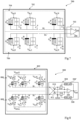
- FIG. 7 schematically represents a neural circuit based on RRAM 700 having a differential structure according to one embodiment of the present description.
- the neural circuit 700 comprises a differential input stage 702 and an output stage 703 including the comparator 206.
- the differential input stage 702 is similar to the input stage 302 in that it comprises a set 704 of N+1 branches each comprising a corresponding resistive element G i P , i ⁇ ⁇ 0 , ..., N ⁇ which has an associated parasitic capacitance VS i P , i ⁇ ⁇ 0 , ..., N ⁇ .
- Each resistive element G i P , i E ⁇ 0,...,N ⁇ also has one of its electrodes, for example its upper electrode, connected to the common conductive line SL.
- each resistive element G i P , i ⁇ ⁇ 0 , ...,N ⁇ which is for example its lower electrode, is connected directly to the corresponding voltage V in,i , i ⁇ ⁇ 0, ..., N ⁇ supplied by another neuronal circuit of the neural network or by an input node of the neural network.
- the common conductive line SL is connected to the positive input of comparator 206.
- the differential input stage 702 further comprises a set 706 of N+1 additional branches, each comprising a corresponding resistive element G i B , i ⁇ ⁇ 0 , ..., N ⁇ which has an associated parasitic capacitance VS i B , i ⁇ ⁇ 0, ...,N ⁇ .
- Each resistive element G i B , i ⁇ ⁇ 0 , ..., N ⁇ also has one of its electrodes, for example its upper electrode, connected to another common conductive line SL'.
- the other electrode of each resistive element G i B , i ⁇ ⁇ 0, ...,N ⁇ which is for example its lower electrode, is connected directly to the corresponding voltage V in,i , i ⁇ ⁇ 0, ...
- the resistive elements G i P And G i B are related, for example by their lower electrode, at the same voltage V in,i , i ⁇ ⁇ 0 , ..., N ⁇ .
- the common conductive line SL will be charged by the sum of the currents circulating in each of the N+1 branches of the set 704, while the common conductive line SL' will be charged by the sum of the currents circulating in each of the N+ 1 branches of the assembly 706.
- the comparator 206 is then used to detect the moment at which the voltage V SL on the common conducting line SL exceeds the voltage V SL ' on the common conducting line SL' and to generate a corresponding output transition of the output voltage V out .
- each synaptic coefficient is represented by the conductivity value G i P ⁇ G i B , i ⁇ ⁇ 0, ... , N ⁇ , when the synaptic coefficient is negative if G i B > G i P .
- the neural circuit 800 includes a differential input stage 802 and an output stage 804.
- the input stage 802 comprises two sets 806 and 808 of N+1 branches, each comprising the resistive elements G i P And G i B , i ⁇ ⁇ 0, ... , N ⁇ .
- Each resistive element G i P And G i B has one of its electrodes, for example its lower electrode, connected to the supply voltage rail V bot via a corresponding transistor T i P And T i B .
- Each transistor T i P , T i B has for example its gate connected to receive the corresponding voltage V in,i .
- the output stage 804 comprises a transistor 810 and a transistor 812.
- the transistor 810 is for example connected by its main conduction nodes between the common conductive line SL and the ground voltage rail.
- the transistor 812 is for example connected by its main conduction nodes between the common conductive line SL' and the ground voltage rail.
- the gate of transistor 810 is connected to the common conductive line SL', while the gate of transistor 812 is connected to the common conductive line SL.
- the output stage 804 further comprises the comparator 206, the positive input of which is connected to the common conductive line SL and the negative input of which is connected to the common conductive line SL'.
- the comparator 206 is used to generate a corresponding output transition of the output voltage V out based on the relative levels of the voltages V SL and V SL ' on the common conductive lines SL and SL'.
- the output of the comparator 206 is connected to the gate of the transistor 510 via the delay circuit 508 and, similarly, to the gate of a transistor 510' via a delay circuit 508'.
- the transistor 510 of the figure 8 is connected between the common conductive line SL and the ground rail.
- the 510 transistor of the figure 5 the transistor 510 of the figure 8 is connected between the common conductive line SL and the ground rail.
- the implementation of the output stage 804 allows two different operating regimes.
- the input voltages V in,i , i ⁇ ⁇ 0, ..., N ⁇ are continuous analog voltage levels, which are for example fixed or substantially fixed over time.
- the voltage of one of the common conductive lines SL or SL' increases and exceeds the voltage on the other common conductive line. This will cause either transistor 810 and 812 to gradually discharge the lower voltage common conductive line to ground.
- the comparator 206 will generate a voltage pulse on the output voltage V out , the duration of the voltage pulse being a function of the delay introduced by the delay circuits 508, 508'.
- the threshold comparison is for example a function of the structure of the comparator 206 and the current leakage which passes to ground through each of the transistors 510 and 510'.
- the two delay circuits 508, 508' and transistors 510, 510' also cause, for example, the resetting of the voltage on the common conductive lines SL and SL' to a voltage close to the ground voltage, a delay after a voltage transition of the output voltage V out .
- resetting the voltage on the common conductive lines SL and SL' in turn resets the output voltage V out of the comparator 206.
- FIG. 9 is a timing diagram representing voltages present in the RRAM-based pulse neural circuit 800 according to an exemplary embodiment.
- the temporal evolutions of the voltages V SL and V SL' are represented by curves 900 and 902 and are initially close to ground.
- the output voltage V out is represented by a curve 904.
- the voltages on the common conductive lines SL and SL' begin to increase at a time t 0 following the application of analog input voltages V in,i , i ⁇ ⁇ 0, ..., NOT ⁇ .
- the voltage V SL exceeds the voltage V SL' , causing the transistor 812 to conduct more than the transistor 810.
- the voltage V SL ' is thus discharged to the ground voltage, while the voltage V SL continues to increase.
- the difference between the voltages V SL and V SL ' exceeds the value of the threshold voltage V th .
- the comparator 206 generates the voltage pulse on the output voltage V out , the duration of which depends on the delay circuits 508, 508', which for example apply substantially the same delay as each other.
- the voltages V SL and V SL ' are thus reset to a value close to ground via the transistors 510, 510' activated by the delay circuits 508.
- the voltages V SL and V SL ' After resetting the voltages V SL and V SL ', they remain, for example, low until a time t 3 .
- the voltages V SL and V SL ' are discharged after a fixed time delay of the delay circuit 508, 508'. Once this time delay has elapsed, the lines SL and SL' are for example left floating until a new neuronal operating cycle begins. A new cycle of neuronal operation therefore begins and, this time, it is for example the voltage V SL ' which exceeds the voltage V SL .
- the voltages V SL and V SL ' are then reset, leading to the generation of the voltage pulse V out at a time t 4 .
- the load of the conductive lines SL and SL' differs from the first operating regime, the input voltages V in,i , i ⁇ ⁇ 0, ..., N ⁇ comprising voltage pulses for example in the form of voltage pulsations.
- the rows of transistors T i P And T i B , i ⁇ ⁇ 0, ... , N ⁇ receive the voltage pulses, coming for example from other neurons in the neuronal circuit.
- the voltage pulses cause an accumulation of charges on the common conductive lines SL and SL'.
- FIG. 10 is a chronogram representing an example of the temporal evolution of the input voltages V in,i , i ⁇ ⁇ 0, ..., N ⁇ at the transistor gates T i P And T i B , voltages V SL and V SL ' on the common conductive lines SL and SL' and the voltage V out , in accordance with the second operating regime of circuit 800 is represented in Figure 10 .
- Figure 10 Indeed, for the sake of clarity, we consider a case in which input pulses are present on only the input voltages V in, 0 and V in, 1 of the transistors T 0 P , T 0 B And T 1 P , T 1 B of the neural circuit 800.
- the transistors T 0 P And T 0 B receive a voltage pulse V ⁇ in ,0 ⁇ 1000, generating a first accumulation of charges on the common conductive lines SL and SL'. Consequently, the voltages V SL and V SL ', represented respectively by curves 1002 and 1004, increase suddenly and these voltages are applied to the gates of the transistors 810 and 812, leading to a progressive and relatively slow decrease in the two voltages V SL and V SL '.
- the transistors T 1 P And T 1 B receive a pulse of voltage V ⁇ in , 1 ⁇ 1006.
- each of the voltage pulses at times t 0 , t 1 , t 2 and t 3 causes the voltage V SL ' to be greater than the voltage V SL , and therefore the transistor 810 conducts more than the transistor 812, bringing the voltage V SL to decrease more quickly than the voltage V SL '.
- a new neuronal cycle then begins for example and, at a time t 5 , the voltage V SL becomes greater than the voltage V SL ' by a value greater than the threshold voltage V th .
- FIG. 11 schematically represents an analog neural circuit based on RRAM 1100 having a differential structure according to another embodiment of the present description.
- the neural circuit 1100 includes the differential input stage 702 and an output stage 1104.
- Output stage 1104 is similar to output stage 804 of the figure 8 in that it comprises the transistors 810 and 812 connecting the common conductive lines SL and SL' to ground and having their gates connected to the opposite common conductive line.
- the output stage 1104 differs from the output stage 804 in that the comparator 206 is replaced by a voltage amplifier 1106, which is for example a differential amplifier, and has for example unity gain and delay circuits 508 , 508' and transistors 510, 510' are omitted. Therefore, the tension output V out is generated in the form of an analog direct voltage and no longer includes pulsations or voltage pulses, unlike the case of circuit 800.
- the output voltage V out is for example the membrane potential of the neuronal circuit and is equal to the voltage difference V SL - V SL' . This allows positive or negative values of the output voltage V out to be encoded.
- FIG. 12 is a timing diagram representing voltages present in the RRAM-based analog neural circuit 1100 according to an exemplary embodiment of the present description.
- the values of the voltages V SL and V SL ' on the conductive lines are represented respectively by dotted line curves 1200 and 1202, while the output voltage V out is represented by a continuous curve 1204.
- the voltages V SL , V SL ' and V out are close to the ground voltage.
- the voltage on the conducting line SL is greater than the voltage on the conducting line SL'. Consequently, the output voltage V out is positive between times t 0 and t 1 .
- the voltage on the conductive line SL' becomes greater than the voltage on the conductive line SL, consequently, the output voltage V out becomes negative.
- the output voltage V out is positive between time t 2 and time t 3 , negative between time t 3 and time t 4 , positive between time t 4 and time t 5 , negative between time t 5 and time t 6 , then positive after time t 6 .
- Figure 11 represents an example of analog operation applied to a structure differential of the neural circuit similar to that of the figure 8
- the person skilled in the art will understand that such analog operation could be applied to the non-differential neural circuits 200, 300 of the figure 2 And 3 respectively or to the differential neural circuit 700 of the figure, which does not include the transistors 810, 812. This involves for example replacing, in the different embodiments, the comparator 206 by the voltage amplifier 1106.
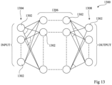
- FIG. 13 schematically represents a neural network 1300 consisting of a plurality of neural circuits 1302 according to an exemplary embodiment of the present description.
- the neural network 1300 includes a plurality of layers and each layer of the neural network 1300 is made up of a plurality of neural circuits 1300.
- the network includes an input layer 1304 comprising a plurality of neural circuits 1302, one or more hidden layers 1306, each hidden layer comprising a plurality of neural circuits 1302, and an output layer 1308 comprising a plurality of neural circuits 1302.
- the neural circuits 1302 of the input layer 1304 receive for example one or more voltages from an INPUT signal, for example via one or more input nodes of the circuit.
- the output voltages V out generated by the neural circuits of the output layer 1308 make it possible, for example, to generate an OUTPUT output signal.
- the neural circuits 1302 of each layer of the network 1300 are for example produced by the same circuit among the different neural circuits described here, or by a plurality of different neural circuits among the different neural circuits described here, for example by one or more of the neural circuits 200, 300, 500, 700, 800 or 1100 of the figures 2 , 3 , 5 , 7 , 8 And 11 respectively.
- each layer all the neural circuits 1302 are implemented in the same way among the embodiments described in relation to the figures 2 , 3 , 5 , 7 , 8 And 11 .
- the modes of implementation of the neural circuit change for example from one layer to another.
Landscapes
- Engineering & Computer Science (AREA)
- Physics & Mathematics (AREA)
- Health & Medical Sciences (AREA)
- Life Sciences & Earth Sciences (AREA)
- Biomedical Technology (AREA)
- Biophysics (AREA)
- Theoretical Computer Science (AREA)
- Evolutionary Computation (AREA)
- General Engineering & Computer Science (AREA)
- Data Mining & Analysis (AREA)
- Artificial Intelligence (AREA)
- General Health & Medical Sciences (AREA)
- Molecular Biology (AREA)
- Computing Systems (AREA)
- Computational Linguistics (AREA)
- General Physics & Mathematics (AREA)
- Mathematical Physics (AREA)
- Software Systems (AREA)
- Neurology (AREA)
- Logic Circuits (AREA)
- Semiconductor Memories (AREA)
Applications Claiming Priority (1)
| Application Number | Priority Date | Filing Date | Title |
|---|---|---|---|
| FR2210609A FR3140974B1 (fr) | 2022-10-14 | 2022-10-14 | Circuit neuromorphique |
Publications (1)
| Publication Number | Publication Date |
|---|---|
| EP4354352A1 true EP4354352A1 (de) | 2024-04-17 |
Family
ID=85221967
Family Applications (1)
| Application Number | Title | Priority Date | Filing Date |
|---|---|---|---|
| EP23203111.2A Pending EP4354352A1 (de) | 2022-10-14 | 2023-10-12 | Neuromorphe schaltung |
Country Status (2)
| Country | Link |
|---|---|
| EP (1) | EP4354352A1 (de) |
| FR (1) | FR3140974B1 (de) |
Citations (1)
| Publication number | Priority date | Publication date | Assignee | Title |
|---|---|---|---|---|
| US20210232905A1 (en) * | 2020-01-24 | 2021-07-29 | Commissarial à I'Energie Atomique et aux Energies Alternatices | Neuromorphic architecture |
-
2022
- 2022-10-14 FR FR2210609A patent/FR3140974B1/fr active Active
-
2023
- 2023-10-12 EP EP23203111.2A patent/EP4354352A1/de active Pending
Patent Citations (1)
| Publication number | Priority date | Publication date | Assignee | Title |
|---|---|---|---|---|
| US20210232905A1 (en) * | 2020-01-24 | 2021-07-29 | Commissarial à I'Energie Atomique et aux Energies Alternatices | Neuromorphic architecture |
Non-Patent Citations (4)
| Title |
|---|
| BERDAN, RADU, NATURE ELECTRONICS, vol. 3, no. 5, 2020 |
| GABRIEL MARANHÃO ET AL: "Low-power hybrid memristor-CMOS spiking neuromorphic STDP learning system", IET CIRCUITS DEVICES AND SYSTEMS, THE INSTITUTION OF ENGINEERING AND TECHNOLOGY, GB, vol. 15, no. 3, 11 March 2021 (2021-03-11), pages 237 - 250, XP006105755, ISSN: 1751-858X, DOI: 10.1049/CDS2.12018 * |
| REN KUAN ET AL: "VETAM-M: A General Model for Voltage-Controlled Memcapacitive-Coupled Memristors", IEEE TRANSACTIONS ON CIRCUITS AND SYSTEMS II: EXPRESS BRIEFS, IEEE, USA, vol. 69, no. 3, 12 August 2021 (2021-08-12), pages 1717 - 1721, XP011903247, ISSN: 1549-7747, [retrieved on 20220315], DOI: 10.1109/TCSII.2021.3103553 * |
| THOMAS SHERIN A ET AL: "Analysis of Parasitic Effects in a Crossbar in CMOS Based Neuromorphic System for Pattern Recognition Using Memristive Synapses", IEEE TRANSACTIONS ON NANOTECHNOLOGY, IEEE, USA, vol. 21, 13 July 2022 (2022-07-13), pages 380 - 389, XP011915730, ISSN: 1536-125X, [retrieved on 20220714], DOI: 10.1109/TNANO.2022.3190903 * |
Also Published As
| Publication number | Publication date |
|---|---|
| FR3140974A1 (fr) | 2024-04-19 |
| FR3140974B1 (fr) | 2025-04-11 |
Similar Documents
| Publication | Publication Date | Title |
|---|---|---|
| EP3663988B1 (de) | Künstliches neuron für neuromorphen chip mit resistiven synapsen | |
| EP3794514B1 (de) | Geschaltete künstliche synapse | |
| FR3050050A1 (fr) | Neurone artificiel | |
| FR2665036A1 (fr) | Circuit pour retarder un signal. | |
| FR3003062A1 (fr) | Organe a neurone artificiel et memristor | |
| FR3072564B1 (fr) | Capteur optique | |
| FR3089037A1 (fr) | Circuit neuronal apte à mettre en œuvre un apprentissage synaptique | |
| FR2529726A1 (fr) | Amplificateur a seuil prevu pour la fabrication en circuit integre | |
| WO2022171632A1 (fr) | Circuit neuromorphique et procédé d'entraînement associé | |
| FR3064383A1 (fr) | Dispositif integre de neurone artificiel | |
| EP1608069B1 (de) | Verfahren zur Steuerung eines Analogschalters | |
| EP3806162B1 (de) | Löschschaltung einer spad | |
| FR2532797A1 (fr) | Amplificateur differentiel | |
| EP4354352A1 (de) | Neuromorphe schaltung | |
| FR2722625A1 (fr) | Convertisseur a/n a comparaison multiple utilisant le principe d'interpolation | |
| EP1727147B1 (de) | Leseverstärker für einen dynamischen Speicher | |
| FR2914516A1 (fr) | Circuit electronique amplificateur comprenant une paire differentielle et un systeme de contre-reaction. | |
| FR3071116A1 (fr) | Dispositif modifiant la valeur d'impedance d'une resistance de reference | |
| EP1647091A2 (de) | Spannungsverstärker mit niedrigem verbrauch | |
| FR2499788A1 (fr) | Circuit generateur d'impulsions utilisant une source de courant et ensemble de memorisation utilisant un tel circuit | |
| EP4020479A1 (de) | Differentielles lesen eines rram-speichers mit geringem stromverbrauch | |
| EP4012924B1 (de) | Dynamischer komparator | |
| FR3115382A1 (fr) | Neurone artificiel | |
| EP4030621A1 (de) | Dynamischer komparator | |
| FR2682801A1 (fr) | Circuit pour produire une tension d'alimentation en courant interne dans un dispositif de memoire a semiconducteurs. |
Legal Events
| Date | Code | Title | Description |
|---|---|---|---|
| PUAI | Public reference made under article 153(3) epc to a published international application that has entered the european phase |
Free format text: ORIGINAL CODE: 0009012 |
|
| STAA | Information on the status of an ep patent application or granted ep patent |
Free format text: STATUS: REQUEST FOR EXAMINATION WAS MADE |
|
| 17P | Request for examination filed |
Effective date: 20231012 |
|
| AK | Designated contracting states |
Kind code of ref document: A1 Designated state(s): AL AT BE BG CH CY CZ DE DK EE ES FI FR GB GR HR HU IE IS IT LI LT LU LV MC ME MK MT NL NO PL PT RO RS SE SI SK SM TR |
|
| RAP3 | Party data changed (applicant data changed or rights of an application transferred) |
Owner name: COMMISSARIAT A L'ENERGIE ATOMIQUE ET AUX ENERGIESALTERNATIVES |