EP4353301A2 - Données magnétoélectriques et alimentation de biodispositifs miniatures à amplitude et forme d'onde accordables - Google Patents
Données magnétoélectriques et alimentation de biodispositifs miniatures à amplitude et forme d'onde accordables Download PDFInfo
- Publication number
- EP4353301A2 EP4353301A2 EP24160440.4A EP24160440A EP4353301A2 EP 4353301 A2 EP4353301 A2 EP 4353301A2 EP 24160440 A EP24160440 A EP 24160440A EP 4353301 A2 EP4353301 A2 EP 4353301A2
- Authority
- EP
- European Patent Office
- Prior art keywords
- film
- magnetic field
- magnetoelectric
- stimulation
- voltage
- Prior art date
- Legal status (The legal status is an assumption and is not a legal conclusion. Google has not performed a legal analysis and makes no representation as to the accuracy of the status listed.)
- Pending
Links
- 238000000034 method Methods 0.000 claims abstract description 78
- 229920002981 polyvinylidene fluoride Polymers 0.000 claims description 67
- 239000003990 capacitor Substances 0.000 claims description 23
- 229910052451 lead zirconate titanate Inorganic materials 0.000 claims description 23
- 239000002033 PVDF binder Substances 0.000 claims description 12
- HFGPZNIAWCZYJU-UHFFFAOYSA-N lead zirconate titanate Chemical compound [O-2].[O-2].[O-2].[O-2].[O-2].[Ti+4].[Zr+4].[Pb+2] HFGPZNIAWCZYJU-UHFFFAOYSA-N 0.000 claims description 9
- 230000000638 stimulation Effects 0.000 abstract description 172
- 230000001537 neural effect Effects 0.000 abstract description 86
- 238000003860 storage Methods 0.000 abstract description 18
- 239000010408 film Substances 0.000 description 337
- 239000000463 material Substances 0.000 description 57
- 230000002051 biphasic effect Effects 0.000 description 56
- XLOMVQKBTHCTTD-UHFFFAOYSA-N Zinc monoxide Chemical compound [Zn]=O XLOMVQKBTHCTTD-UHFFFAOYSA-N 0.000 description 50
- 210000001519 tissue Anatomy 0.000 description 49
- 238000012360 testing method Methods 0.000 description 44
- 238000012546 transfer Methods 0.000 description 43
- 210000004027 cell Anatomy 0.000 description 41
- 239000007943 implant Substances 0.000 description 36
- 210000004556 brain Anatomy 0.000 description 34
- 241001465754 Metazoa Species 0.000 description 28
- 238000002474 experimental method Methods 0.000 description 26
- 241000700159 Rattus Species 0.000 description 25
- 238000004519 manufacturing process Methods 0.000 description 21
- 210000003625 skull Anatomy 0.000 description 21
- 239000011787 zinc oxide Substances 0.000 description 21
- 238000005516 engineering process Methods 0.000 description 19
- 230000000694 effects Effects 0.000 description 17
- 230000004936 stimulating effect Effects 0.000 description 17
- 230000006870 function Effects 0.000 description 16
- 230000036982 action potential Effects 0.000 description 15
- 239000002105 nanoparticle Substances 0.000 description 15
- 238000013461 design Methods 0.000 description 14
- 238000010586 diagram Methods 0.000 description 14
- 238000000338 in vitro Methods 0.000 description 14
- 239000000243 solution Substances 0.000 description 14
- 230000008878 coupling Effects 0.000 description 13
- 238000010168 coupling process Methods 0.000 description 13
- 238000005859 coupling reaction Methods 0.000 description 13
- 229910000697 metglas Inorganic materials 0.000 description 13
- 230000001225 therapeutic effect Effects 0.000 description 13
- FAPWRFPIFSIZLT-UHFFFAOYSA-M Sodium chloride Chemical compound [Na+].[Cl-] FAPWRFPIFSIZLT-UHFFFAOYSA-M 0.000 description 12
- 239000002070 nanowire Substances 0.000 description 12
- 230000004044 response Effects 0.000 description 12
- 230000003044 adaptive effect Effects 0.000 description 11
- 238000013459 approach Methods 0.000 description 11
- 230000008901 benefit Effects 0.000 description 10
- 210000000988 bone and bone Anatomy 0.000 description 10
- 230000001965 increasing effect Effects 0.000 description 10
- 238000004088 simulation Methods 0.000 description 10
- 238000010521 absorption reaction Methods 0.000 description 9
- 239000000428 dust Substances 0.000 description 9
- 238000007726 management method Methods 0.000 description 9
- 239000011780 sodium chloride Substances 0.000 description 9
- ZWEHNKRNPOVVGH-UHFFFAOYSA-N 2-Butanone Chemical compound CCC(C)=O ZWEHNKRNPOVVGH-UHFFFAOYSA-N 0.000 description 8
- 239000004593 Epoxy Substances 0.000 description 8
- 230000005540 biological transmission Effects 0.000 description 8
- 230000001939 inductive effect Effects 0.000 description 8
- 238000005259 measurement Methods 0.000 description 8
- 238000012384 transportation and delivery Methods 0.000 description 8
- 230000006399 behavior Effects 0.000 description 7
- 230000003542 behavioural effect Effects 0.000 description 7
- 238000006243 chemical reaction Methods 0.000 description 7
- 230000001684 chronic effect Effects 0.000 description 7
- 208000037265 diseases, disorders, signs and symptoms Diseases 0.000 description 7
- 230000002829 reductive effect Effects 0.000 description 7
- 238000002604 ultrasonography Methods 0.000 description 7
- VRBFTYUMFJWSJY-UHFFFAOYSA-N 28804-46-8 Chemical compound ClC1CC(C=C2)=CC=C2C(Cl)CC2=CC=C1C=C2 VRBFTYUMFJWSJY-UHFFFAOYSA-N 0.000 description 6
- 208000018737 Parkinson disease Diseases 0.000 description 6
- 241000283984 Rodentia Species 0.000 description 6
- UIIMBOGNXHQVGW-UHFFFAOYSA-M Sodium bicarbonate Chemical compound [Na+].OC([O-])=O UIIMBOGNXHQVGW-UHFFFAOYSA-M 0.000 description 6
- 239000002131 composite material Substances 0.000 description 6
- LOKCTEFSRHRXRJ-UHFFFAOYSA-I dipotassium trisodium dihydrogen phosphate hydrogen phosphate dichloride Chemical compound P(=O)(O)(O)[O-].[K+].P(=O)(O)([O-])[O-].[Na+].[Na+].[Cl-].[K+].[Cl-].[Na+] LOKCTEFSRHRXRJ-UHFFFAOYSA-I 0.000 description 6
- 238000003306 harvesting Methods 0.000 description 6
- 210000003128 head Anatomy 0.000 description 6
- 238000010438 heat treatment Methods 0.000 description 6
- 230000001976 improved effect Effects 0.000 description 6
- 230000007774 longterm Effects 0.000 description 6
- 241000243251 Hydra Species 0.000 description 5
- 230000032683 aging Effects 0.000 description 5
- 230000008859 change Effects 0.000 description 5
- 230000001419 dependent effect Effects 0.000 description 5
- 230000005684 electric field Effects 0.000 description 5
- 238000005538 encapsulation Methods 0.000 description 5
- 230000007062 hydrolysis Effects 0.000 description 5
- 238000006460 hydrolysis reaction Methods 0.000 description 5
- 238000001727 in vivo Methods 0.000 description 5
- QRXWMOHMRWLFEY-UHFFFAOYSA-N isoniazide Chemical compound NNC(=O)C1=CC=NC=C1 QRXWMOHMRWLFEY-UHFFFAOYSA-N 0.000 description 5
- 210000002569 neuron Anatomy 0.000 description 5
- 239000002953 phosphate buffered saline Substances 0.000 description 5
- BASFCYQUMIYNBI-UHFFFAOYSA-N platinum Chemical compound [Pt] BASFCYQUMIYNBI-UHFFFAOYSA-N 0.000 description 5
- 230000001105 regulatory effect Effects 0.000 description 5
- 238000012421 spiking Methods 0.000 description 5
- 210000004281 subthalamic nucleus Anatomy 0.000 description 5
- UXVMQQNJUSDDNG-UHFFFAOYSA-L Calcium chloride Chemical compound [Cl-].[Cl-].[Ca+2] UXVMQQNJUSDDNG-UHFFFAOYSA-L 0.000 description 4
- PIWKPBJCKXDKJR-UHFFFAOYSA-N Isoflurane Chemical compound FC(F)OC(Cl)C(F)(F)F PIWKPBJCKXDKJR-UHFFFAOYSA-N 0.000 description 4
- TWRXJAOTZQYOKJ-UHFFFAOYSA-L Magnesium chloride Chemical compound [Mg+2].[Cl-].[Cl-] TWRXJAOTZQYOKJ-UHFFFAOYSA-L 0.000 description 4
- CSNNHWWHGAXBCP-UHFFFAOYSA-L Magnesium sulfate Chemical compound [Mg+2].[O-][S+2]([O-])([O-])[O-] CSNNHWWHGAXBCP-UHFFFAOYSA-L 0.000 description 4
- 241000699670 Mus sp. Species 0.000 description 4
- 239000004642 Polyimide Substances 0.000 description 4
- 230000003213 activating effect Effects 0.000 description 4
- 230000004913 activation Effects 0.000 description 4
- 239000001110 calcium chloride Substances 0.000 description 4
- 235000011148 calcium chloride Nutrition 0.000 description 4
- 229910001628 calcium chloride Inorganic materials 0.000 description 4
- 238000004891 communication Methods 0.000 description 4
- 230000007423 decrease Effects 0.000 description 4
- 208000035475 disorder Diseases 0.000 description 4
- 238000005868 electrolysis reaction Methods 0.000 description 4
- 238000004146 energy storage Methods 0.000 description 4
- 230000007613 environmental effect Effects 0.000 description 4
- 230000005284 excitation Effects 0.000 description 4
- 238000002073 fluorescence micrograph Methods 0.000 description 4
- 230000006698 induction Effects 0.000 description 4
- 208000015181 infectious disease Diseases 0.000 description 4
- 230000010354 integration Effects 0.000 description 4
- 229960002725 isoflurane Drugs 0.000 description 4
- 210000004245 medial forebrain bundle Anatomy 0.000 description 4
- 238000001000 micrograph Methods 0.000 description 4
- 238000012544 monitoring process Methods 0.000 description 4
- 238000007427 paired t-test Methods 0.000 description 4
- 229920000052 poly(p-xylylene) Polymers 0.000 description 4
- 229920001721 polyimide Polymers 0.000 description 4
- 238000011084 recovery Methods 0.000 description 4
- 230000009467 reduction Effects 0.000 description 4
- 238000011160 research Methods 0.000 description 4
- 238000002560 therapeutic procedure Methods 0.000 description 4
- 239000010409 thin film Substances 0.000 description 4
- ONDPHDOFVYQSGI-UHFFFAOYSA-N zinc nitrate Chemical compound [Zn+2].[O-][N+]([O-])=O.[O-][N+]([O-])=O ONDPHDOFVYQSGI-UHFFFAOYSA-N 0.000 description 4
- JKMHFZQWWAIEOD-UHFFFAOYSA-N 2-[4-(2-hydroxyethyl)piperazin-1-yl]ethanesulfonic acid Chemical compound OCC[NH+]1CCN(CCS([O-])(=O)=O)CC1 JKMHFZQWWAIEOD-UHFFFAOYSA-N 0.000 description 3
- OYPRJOBELJOOCE-UHFFFAOYSA-N Calcium Chemical compound [Ca] OYPRJOBELJOOCE-UHFFFAOYSA-N 0.000 description 3
- HCYAFALTSJYZDH-UHFFFAOYSA-N Desimpramine Chemical compound C1CC2=CC=CC=C2N(CCCNC)C2=CC=CC=C21 HCYAFALTSJYZDH-UHFFFAOYSA-N 0.000 description 3
- WQZGKKKJIJFFOK-GASJEMHNSA-N Glucose Natural products OC[C@H]1OC(O)[C@H](O)[C@@H](O)[C@@H]1O WQZGKKKJIJFFOK-GASJEMHNSA-N 0.000 description 3
- 239000004472 Lysine Substances 0.000 description 3
- 241000699666 Mus <mouse, genus> Species 0.000 description 3
- 108010052164 Sodium Channels Proteins 0.000 description 3
- 102000018674 Sodium Channels Human genes 0.000 description 3
- 238000002441 X-ray diffraction Methods 0.000 description 3
- 239000011575 calcium Substances 0.000 description 3
- 229910052791 calcium Inorganic materials 0.000 description 3
- 230000001413 cellular effect Effects 0.000 description 3
- 238000011281 clinical therapy Methods 0.000 description 3
- 230000000295 complement effect Effects 0.000 description 3
- 229960003914 desipramine Drugs 0.000 description 3
- 201000010099 disease Diseases 0.000 description 3
- 239000000284 extract Substances 0.000 description 3
- 238000000799 fluorescence microscopy Methods 0.000 description 3
- 210000004744 fore-foot Anatomy 0.000 description 3
- 239000008103 glucose Substances 0.000 description 3
- 230000012010 growth Effects 0.000 description 3
- 238000003384 imaging method Methods 0.000 description 3
- 238000002347 injection Methods 0.000 description 3
- 239000007924 injection Substances 0.000 description 3
- 230000002045 lasting effect Effects 0.000 description 3
- 230000003902 lesion Effects 0.000 description 3
- 230000005690 magnetoelectric effect Effects 0.000 description 3
- 230000007246 mechanism Effects 0.000 description 3
- 239000000203 mixture Substances 0.000 description 3
- 235000019799 monosodium phosphate Nutrition 0.000 description 3
- 230000003287 optical effect Effects 0.000 description 3
- 210000000578 peripheral nerve Anatomy 0.000 description 3
- 229920000642 polymer Polymers 0.000 description 3
- 239000000523 sample Substances 0.000 description 3
- 239000004065 semiconductor Substances 0.000 description 3
- 230000035945 sensitivity Effects 0.000 description 3
- 235000017557 sodium bicarbonate Nutrition 0.000 description 3
- 229910000030 sodium bicarbonate Inorganic materials 0.000 description 3
- AJPJDKMHJJGVTQ-UHFFFAOYSA-M sodium dihydrogen phosphate Chemical compound [Na+].OP(O)([O-])=O AJPJDKMHJJGVTQ-UHFFFAOYSA-M 0.000 description 3
- 229910000162 sodium phosphate Inorganic materials 0.000 description 3
- 239000007779 soft material Substances 0.000 description 3
- 210000000278 spinal cord Anatomy 0.000 description 3
- 230000035882 stress Effects 0.000 description 3
- 239000000758 substrate Substances 0.000 description 3
- 238000011282 treatment Methods 0.000 description 3
- 206010002091 Anaesthesia Diseases 0.000 description 2
- 239000007995 HEPES buffer Substances 0.000 description 2
- 241000282412 Homo Species 0.000 description 2
- 238000012404 In vitro experiment Methods 0.000 description 2
- 102000004310 Ion Channels Human genes 0.000 description 2
- 108090000862 Ion Channels Proteins 0.000 description 2
- 241001124569 Lycaenidae Species 0.000 description 2
- 101710138657 Neurotoxin Proteins 0.000 description 2
- 208000021384 Obsessive-Compulsive disease Diseases 0.000 description 2
- 241000209094 Oryza Species 0.000 description 2
- 235000007164 Oryza sativa Nutrition 0.000 description 2
- 208000002193 Pain Diseases 0.000 description 2
- 229920002367 Polyisobutene Polymers 0.000 description 2
- 102000004257 Potassium Channel Human genes 0.000 description 2
- BQCADISMDOOEFD-UHFFFAOYSA-N Silver Chemical compound [Ag] BQCADISMDOOEFD-UHFFFAOYSA-N 0.000 description 2
- ZOIORXHNWRGPMV-UHFFFAOYSA-N acetic acid;zinc Chemical compound [Zn].CC(O)=O.CC(O)=O ZOIORXHNWRGPMV-UHFFFAOYSA-N 0.000 description 2
- NIXOWILDQLNWCW-UHFFFAOYSA-N acrylic acid group Chemical group C(C=C)(=O)O NIXOWILDQLNWCW-UHFFFAOYSA-N 0.000 description 2
- 230000001464 adherent effect Effects 0.000 description 2
- 229910045601 alloy Inorganic materials 0.000 description 2
- 239000000956 alloy Substances 0.000 description 2
- PNEYBMLMFCGWSK-UHFFFAOYSA-N aluminium oxide Inorganic materials [O-2].[O-2].[O-2].[Al+3].[Al+3] PNEYBMLMFCGWSK-UHFFFAOYSA-N 0.000 description 2
- 230000037005 anaesthesia Effects 0.000 description 2
- 239000007864 aqueous solution Substances 0.000 description 2
- 229940072107 ascorbate Drugs 0.000 description 2
- 239000011668 ascorbic acid Substances 0.000 description 2
- 238000000231 atomic layer deposition Methods 0.000 description 2
- 230000004888 barrier function Effects 0.000 description 2
- 230000009286 beneficial effect Effects 0.000 description 2
- BQRGNLJZBFXNCZ-UHFFFAOYSA-N calcein am Chemical compound O1C(=O)C2=CC=CC=C2C21C1=CC(CN(CC(=O)OCOC(C)=O)CC(=O)OCOC(C)=O)=C(OC(C)=O)C=C1OC1=C2C=C(CN(CC(=O)OCOC(C)=O)CC(=O)OCOC(=O)C)C(OC(C)=O)=C1 BQRGNLJZBFXNCZ-UHFFFAOYSA-N 0.000 description 2
- 210000003169 central nervous system Anatomy 0.000 description 2
- 235000013339 cereals Nutrition 0.000 description 2
- 239000003795 chemical substances by application Substances 0.000 description 2
- 230000001143 conditioned effect Effects 0.000 description 2
- 238000007796 conventional method Methods 0.000 description 2
- 229910052593 corundum Inorganic materials 0.000 description 2
- 210000004748 cultured cell Anatomy 0.000 description 2
- 238000011161 development Methods 0.000 description 2
- 230000018109 developmental process Effects 0.000 description 2
- 238000003487 electrochemical reaction Methods 0.000 description 2
- 239000000835 fiber Substances 0.000 description 2
- 238000002513 implantation Methods 0.000 description 2
- 230000003447 ipsilateral effect Effects 0.000 description 2
- 230000000670 limiting effect Effects 0.000 description 2
- 230000005923 long-lasting effect Effects 0.000 description 2
- 229910001629 magnesium chloride Inorganic materials 0.000 description 2
- 229910052943 magnesium sulfate Inorganic materials 0.000 description 2
- 235000019341 magnesium sulphate Nutrition 0.000 description 2
- 230000001404 mediated effect Effects 0.000 description 2
- MYWUZJCMWCOHBA-VIFPVBQESA-N methamphetamine Chemical compound CN[C@@H](C)CC1=CC=CC=C1 MYWUZJCMWCOHBA-VIFPVBQESA-N 0.000 description 2
- 229960001252 methamphetamine Drugs 0.000 description 2
- 230000037230 mobility Effects 0.000 description 2
- 238000012986 modification Methods 0.000 description 2
- 230000004048 modification Effects 0.000 description 2
- 239000002073 nanorod Substances 0.000 description 2
- 230000001423 neocortical effect Effects 0.000 description 2
- 239000002581 neurotoxin Substances 0.000 description 2
- 231100000618 neurotoxin Toxicity 0.000 description 2
- DIVDFFZHCJEHGG-UHFFFAOYSA-N oxidopamine Chemical compound NCCC1=CC(O)=C(O)C=C1O DIVDFFZHCJEHGG-UHFFFAOYSA-N 0.000 description 2
- TWNQGVIAIRXVLR-UHFFFAOYSA-N oxo(oxoalumanyloxy)alumane Chemical compound O=[Al]O[Al]=O TWNQGVIAIRXVLR-UHFFFAOYSA-N 0.000 description 2
- 230000036407 pain Effects 0.000 description 2
- 230000037361 pathway Effects 0.000 description 2
- 230000035515 penetration Effects 0.000 description 2
- 210000001428 peripheral nervous system Anatomy 0.000 description 2
- 229910052697 platinum Inorganic materials 0.000 description 2
- 108020001213 potassium channel Proteins 0.000 description 2
- 238000002360 preparation method Methods 0.000 description 2
- 230000008569 process Effects 0.000 description 2
- 230000001902 propagating effect Effects 0.000 description 2
- 235000009566 rice Nutrition 0.000 description 2
- 238000011808 rodent model Methods 0.000 description 2
- 229920006395 saturated elastomer Polymers 0.000 description 2
- 229910052709 silver Inorganic materials 0.000 description 2
- 239000004332 silver Substances 0.000 description 2
- 230000003997 social interaction Effects 0.000 description 2
- 239000011734 sodium Substances 0.000 description 2
- 239000002904 solvent Substances 0.000 description 2
- 210000000130 stem cell Anatomy 0.000 description 2
- 230000008093 supporting effect Effects 0.000 description 2
- 230000007704 transition Effects 0.000 description 2
- 210000001186 vagus nerve Anatomy 0.000 description 2
- 238000012800 visualization Methods 0.000 description 2
- 229910001845 yogo sapphire Inorganic materials 0.000 description 2
- 239000004246 zinc acetate Substances 0.000 description 2
- UQNAFPHGVPVTAL-UHFFFAOYSA-N 2,3-Dihydroxy-6-nitro-7-sulfamoyl-benzo(f)quinoxaline Chemical compound N1C(=O)C(=O)NC2=C1C=C([N+]([O-])=O)C1=C2C=CC=C1S(=O)(=O)N UQNAFPHGVPVTAL-UHFFFAOYSA-N 0.000 description 1
- 102000003678 AMPA Receptors Human genes 0.000 description 1
- 108090000078 AMPA Receptors Proteins 0.000 description 1
- 229920001817 Agar Polymers 0.000 description 1
- CIWBSHSKHKDKBQ-JLAZNSOCSA-N Ascorbic acid Natural products OC[C@H](O)[C@H]1OC(=O)C(O)=C1O CIWBSHSKHKDKBQ-JLAZNSOCSA-N 0.000 description 1
- 208000008035 Back Pain Diseases 0.000 description 1
- 108091006146 Channels Proteins 0.000 description 1
- 241001573498 Compacta Species 0.000 description 1
- RYGMFSIKBFXOCR-UHFFFAOYSA-N Copper Chemical compound [Cu] RYGMFSIKBFXOCR-UHFFFAOYSA-N 0.000 description 1
- 208000036829 Device dislocation Diseases 0.000 description 1
- KRHYYFGTRYWZRS-UHFFFAOYSA-M Fluoride anion Chemical compound [F-] KRHYYFGTRYWZRS-UHFFFAOYSA-M 0.000 description 1
- 241000243254 Hydra vulgaris Species 0.000 description 1
- DGAQECJNVWCQMB-PUAWFVPOSA-M Ilexoside XXIX Chemical compound C[C@@H]1CC[C@@]2(CC[C@@]3(C(=CC[C@H]4[C@]3(CC[C@@H]5[C@@]4(CC[C@@H](C5(C)C)OS(=O)(=O)[O-])C)C)[C@@H]2[C@]1(C)O)C)C(=O)O[C@H]6[C@@H]([C@H]([C@@H]([C@H](O6)CO)O)O)O.[Na+] DGAQECJNVWCQMB-PUAWFVPOSA-M 0.000 description 1
- 208000001145 Metabolic Syndrome Diseases 0.000 description 1
- 208000034888 Needle issue Diseases 0.000 description 1
- 208000012902 Nervous system disease Diseases 0.000 description 1
- 208000025966 Neurological disease Diseases 0.000 description 1
- 208000013007 Rodent disease Diseases 0.000 description 1
- 238000010162 Tukey test Methods 0.000 description 1
- 201000000690 abdominal obesity-metabolic syndrome Diseases 0.000 description 1
- 239000008272 agar Substances 0.000 description 1
- 230000003444 anaesthetic effect Effects 0.000 description 1
- 230000036592 analgesia Effects 0.000 description 1
- 235000010323 ascorbic acid Nutrition 0.000 description 1
- 230000002238 attenuated effect Effects 0.000 description 1
- 239000012472 biological sample Substances 0.000 description 1
- 230000015572 biosynthetic process Effects 0.000 description 1
- 210000005013 brain tissue Anatomy 0.000 description 1
- 239000000872 buffer Substances 0.000 description 1
- RMRJXGBAOAMLHD-IHFGGWKQSA-N buprenorphine Chemical compound C([C@]12[C@H]3OC=4C(O)=CC=C(C2=4)C[C@@H]2[C@]11CC[C@]3([C@H](C1)[C@](C)(O)C(C)(C)C)OC)CN2CC1CC1 RMRJXGBAOAMLHD-IHFGGWKQSA-N 0.000 description 1
- 229960001736 buprenorphine Drugs 0.000 description 1
- 238000004364 calculation method Methods 0.000 description 1
- 230000015556 catabolic process Effects 0.000 description 1
- 210000005056 cell body Anatomy 0.000 description 1
- 238000004113 cell culture Methods 0.000 description 1
- 230000010261 cell growth Effects 0.000 description 1
- 210000000170 cell membrane Anatomy 0.000 description 1
- 239000003985 ceramic capacitor Substances 0.000 description 1
- 229910010293 ceramic material Inorganic materials 0.000 description 1
- 238000012512 characterization method Methods 0.000 description 1
- 238000005229 chemical vapour deposition Methods 0.000 description 1
- 230000037326 chronic stress Effects 0.000 description 1
- 239000011248 coating agent Substances 0.000 description 1
- 238000000576 coating method Methods 0.000 description 1
- 230000001149 cognitive effect Effects 0.000 description 1
- 239000000084 colloidal system Substances 0.000 description 1
- 238000007428 craniotomy Methods 0.000 description 1
- 239000013078 crystal Substances 0.000 description 1
- 230000001086 cytosolic effect Effects 0.000 description 1
- 230000003247 decreasing effect Effects 0.000 description 1
- 230000007547 defect Effects 0.000 description 1
- 230000004069 differentiation Effects 0.000 description 1
- 238000009792 diffusion process Methods 0.000 description 1
- 238000009826 distribution Methods 0.000 description 1
- 239000003814 drug Substances 0.000 description 1
- 238000012377 drug delivery Methods 0.000 description 1
- 210000001951 dura mater Anatomy 0.000 description 1
- 210000005069 ears Anatomy 0.000 description 1
- 210000003981 ectoderm Anatomy 0.000 description 1
- 230000005672 electromagnetic field Effects 0.000 description 1
- 230000005670 electromagnetic radiation Effects 0.000 description 1
- 238000001523 electrospinning Methods 0.000 description 1
- 230000002708 enhancing effect Effects 0.000 description 1
- 206010015037 epilepsy Diseases 0.000 description 1
- 230000000763 evoking effect Effects 0.000 description 1
- 239000013604 expression vector Substances 0.000 description 1
- 238000001914 filtration Methods 0.000 description 1
- 239000012467 final product Substances 0.000 description 1
- 102000034287 fluorescent proteins Human genes 0.000 description 1
- 108091006047 fluorescent proteins Proteins 0.000 description 1
- 230000004907 flux Effects 0.000 description 1
- 210000001222 gaba-ergic neuron Anatomy 0.000 description 1
- 230000036541 health Effects 0.000 description 1
- 238000005286 illumination Methods 0.000 description 1
- 238000011065 in-situ storage Methods 0.000 description 1
- 238000010348 incorporation Methods 0.000 description 1
- 230000005764 inhibitory process Effects 0.000 description 1
- 230000003993 interaction Effects 0.000 description 1
- 150000002500 ions Chemical class 0.000 description 1
- 210000003734 kidney Anatomy 0.000 description 1
- 210000004185 liver Anatomy 0.000 description 1
- 238000013289 male long evans rat Methods 0.000 description 1
- 238000013017 mechanical damping Methods 0.000 description 1
- 239000012528 membrane Substances 0.000 description 1
- 230000001095 motoneuron effect Effects 0.000 description 1
- 230000004118 muscle contraction Effects 0.000 description 1
- 239000002121 nanofiber Substances 0.000 description 1
- 210000000944 nerve tissue Anatomy 0.000 description 1
- 210000000653 nervous system Anatomy 0.000 description 1
- 230000004007 neuromodulation Effects 0.000 description 1
- 239000002858 neurotransmitter agent Substances 0.000 description 1
- 239000013307 optical fiber Substances 0.000 description 1
- 238000005457 optimization Methods 0.000 description 1
- 238000004806 packaging method and process Methods 0.000 description 1
- 238000002161 passivation Methods 0.000 description 1
- 230000001575 pathological effect Effects 0.000 description 1
- 230000035699 permeability Effects 0.000 description 1
- 239000008055 phosphate buffer solution Substances 0.000 description 1
- 230000006461 physiological response Effects 0.000 description 1
- HWLDNSXPUQTBOD-UHFFFAOYSA-N platinum-iridium alloy Chemical compound [Ir].[Pt] HWLDNSXPUQTBOD-UHFFFAOYSA-N 0.000 description 1
- 229920000136 polysorbate Polymers 0.000 description 1
- 230000035755 proliferation Effects 0.000 description 1
- 210000004129 prosencephalon Anatomy 0.000 description 1
- 230000001681 protective effect Effects 0.000 description 1
- 230000005855 radiation Effects 0.000 description 1
- 230000000630 rising effect Effects 0.000 description 1
- 238000013432 robust analysis Methods 0.000 description 1
- 238000005070 sampling Methods 0.000 description 1
- 238000001878 scanning electron micrograph Methods 0.000 description 1
- 210000003497 sciatic nerve Anatomy 0.000 description 1
- HBMJWWWQQXIZIP-UHFFFAOYSA-N silicon carbide Chemical compound [Si+]#[C-] HBMJWWWQQXIZIP-UHFFFAOYSA-N 0.000 description 1
- 210000004894 snout Anatomy 0.000 description 1
- 230000011273 social behavior Effects 0.000 description 1
- 229910052708 sodium Inorganic materials 0.000 description 1
- 210000004872 soft tissue Anatomy 0.000 description 1
- 230000003238 somatosensory effect Effects 0.000 description 1
- 238000004528 spin coating Methods 0.000 description 1
- 238000013112 stability test Methods 0.000 description 1
- 230000003068 static effect Effects 0.000 description 1
- 238000007619 statistical method Methods 0.000 description 1
- 239000000126 substance Substances 0.000 description 1
- 210000003523 substantia nigra Anatomy 0.000 description 1
- 238000001356 surgical procedure Methods 0.000 description 1
- 208000024891 symptom Diseases 0.000 description 1
- 230000005062 synaptic transmission Effects 0.000 description 1
- 230000002277 temperature effect Effects 0.000 description 1
- CFMYXEVWODSLAX-QOZOJKKESA-N tetrodotoxin Chemical compound O([C@@]([C@H]1O)(O)O[C@H]2[C@@]3(O)CO)[C@H]3[C@@H](O)[C@]11[C@H]2[C@@H](O)N=C(N)N1 CFMYXEVWODSLAX-QOZOJKKESA-N 0.000 description 1
- 229950010357 tetrodotoxin Drugs 0.000 description 1
- CFMYXEVWODSLAX-UHFFFAOYSA-N tetrodotoxin Natural products C12C(O)NC(=N)NC2(C2O)C(O)C3C(CO)(O)C1OC2(O)O3 CFMYXEVWODSLAX-UHFFFAOYSA-N 0.000 description 1
- 230000000451 tissue damage Effects 0.000 description 1
- 231100000827 tissue damage Toxicity 0.000 description 1
- 238000010361 transduction Methods 0.000 description 1
- 230000026683 transduction Effects 0.000 description 1
- 238000001890 transfection Methods 0.000 description 1
- 230000009261 transgenic effect Effects 0.000 description 1
- 230000001960 triggered effect Effects 0.000 description 1
- 239000013598 vector Substances 0.000 description 1
- 238000012795 verification Methods 0.000 description 1
- XLYOFNOQVPJJNP-UHFFFAOYSA-N water Substances O XLYOFNOQVPJJNP-UHFFFAOYSA-N 0.000 description 1
- 238000005303 weighing Methods 0.000 description 1
- 239000011701 zinc Substances 0.000 description 1
Images


Classifications
-
- A—HUMAN NECESSITIES
- A61—MEDICAL OR VETERINARY SCIENCE; HYGIENE
- A61N—ELECTROTHERAPY; MAGNETOTHERAPY; RADIATION THERAPY; ULTRASOUND THERAPY
- A61N1/00—Electrotherapy; Circuits therefor
- A61N1/18—Applying electric currents by contact electrodes
- A61N1/32—Applying electric currents by contact electrodes alternating or intermittent currents
- A61N1/36—Applying electric currents by contact electrodes alternating or intermittent currents for stimulation
- A61N1/372—Arrangements in connection with the implantation of stimulators
- A61N1/37211—Means for communicating with stimulators
- A61N1/37217—Means for communicating with stimulators characterised by the communication link, e.g. acoustic or tactile
- A61N1/37223—Circuits for electromagnetic coupling
-
- A—HUMAN NECESSITIES
- A61—MEDICAL OR VETERINARY SCIENCE; HYGIENE
- A61N—ELECTROTHERAPY; MAGNETOTHERAPY; RADIATION THERAPY; ULTRASOUND THERAPY
- A61N1/00—Electrotherapy; Circuits therefor
- A61N1/18—Applying electric currents by contact electrodes
- A61N1/32—Applying electric currents by contact electrodes alternating or intermittent currents
- A61N1/36—Applying electric currents by contact electrodes alternating or intermittent currents for stimulation
- A61N1/372—Arrangements in connection with the implantation of stimulators
- A61N1/378—Electrical supply
- A61N1/3787—Electrical supply from an external energy source
-
- H—ELECTRICITY
- H10—SEMICONDUCTOR DEVICES; ELECTRIC SOLID-STATE DEVICES NOT OTHERWISE PROVIDED FOR
- H10N—ELECTRIC SOLID-STATE DEVICES NOT OTHERWISE PROVIDED FOR
- H10N35/00—Magnetostrictive devices
- H10N35/101—Magnetostrictive devices with mechanical input and electrical output, e.g. generators, sensors
-
- H—ELECTRICITY
- H10—SEMICONDUCTOR DEVICES; ELECTRIC SOLID-STATE DEVICES NOT OTHERWISE PROVIDED FOR
- H10N—ELECTRIC SOLID-STATE DEVICES NOT OTHERWISE PROVIDED FOR
- H10N35/00—Magnetostrictive devices
- H10N35/80—Constructional details
-
- H—ELECTRICITY
- H10—SEMICONDUCTOR DEVICES; ELECTRIC SOLID-STATE DEVICES NOT OTHERWISE PROVIDED FOR
- H10N—ELECTRIC SOLID-STATE DEVICES NOT OTHERWISE PROVIDED FOR
- H10N35/00—Magnetostrictive devices
- H10N35/80—Constructional details
- H10N35/85—Magnetostrictive active materials
-
- A—HUMAN NECESSITIES
- A61—MEDICAL OR VETERINARY SCIENCE; HYGIENE
- A61N—ELECTROTHERAPY; MAGNETOTHERAPY; RADIATION THERAPY; ULTRASOUND THERAPY
- A61N1/00—Electrotherapy; Circuits therefor
- A61N1/02—Details
- A61N1/04—Electrodes
- A61N1/05—Electrodes for implantation or insertion into the body, e.g. heart electrode
- A61N1/0526—Head electrodes
- A61N1/0529—Electrodes for brain stimulation
- A61N1/0534—Electrodes for deep brain stimulation
-
- H—ELECTRICITY
- H10—SEMICONDUCTOR DEVICES; ELECTRIC SOLID-STATE DEVICES NOT OTHERWISE PROVIDED FOR
- H10N—ELECTRIC SOLID-STATE DEVICES NOT OTHERWISE PROVIDED FOR
- H10N30/00—Piezoelectric or electrostrictive devices
Definitions
- This disclosure relates to apparatus and methods utilizing magnetoelectric neural stimulators with tunable amplitude and waveform.
- this disclosure relates to apparatus and methods configured to charge a charge storage element, transmit data to an implantable wireless neural stimulator and provide a stimulation output.
- a fundamental issue for bioelectronics is the ability to deliver power to miniature devices inside the body.
- Wires provide efficient power transmission, but are common failure points and limit device placement.
- Wireless power by electromagnetic or ultrasound waves must also overcome obstacles.
- wireless power by electromagnetic or ultrasound waves must overcome absorption by the body and impedance mismatches between air, bone, and tissue.
- Conventional methods to wirelessly power neural implants in deep tissue regions of freely moving animals or humans are also usually bulky due to large electromagnetic coils or battery packs with external leads.
- the ability to provide magnetoelectric charging, data transmission and stimulation to an implantable wireless neural stimulator is not provided in existing syste ms.
- the present disclosure provides systems that transmit data to an implanted neural stimulation device with a magnetic field.
- the implanted device includes an electrical circuit that extracts timing and voltage reference from the magnetic field to perform reliable and calibration-free data transmission.
- the circuit transitions between different operation modes (power transfer, data transfer, stimulation) by monitoring the envelop of the magnetic field, which can be more reliable and energy efficient than some conventional methods.
- the present disclosure provides apparatus, systems, and methods that utilize magnetic fields, which suffer little absorption by the body or differences in impedance at interfaces between air, bone, and tissue.
- Exemplary embodiments of the present disclosure utilize magnetoelectric materials that provide miniature energy harvesting from magnetic fields for neural stimulation or to power electronic devices.
- Exemplary embodiments rely on an alternating magnetic field produced by a magnetic field driver that modulates a high frequency (e.g . 20-500 KHz) magnetic field delivered by an electromagnetic coil.
- This magnetic field is at or near the resonant frequency of a magnetoelectric film, which can typically be placed several centimeters from away from the coil.
- the film (a laminate of piezoelectric and magnetoelectric materials) can transform the magnetic field into a high frequency, high voltage electrical signal.
- Exemplary embodiments attach circuit elements to the film to alter the voltage waveform (e.g . to rectify and cap the voltage and current to a stable level for the desired application).
- the electric field from the film can be used to directly stimulate excitable cells in vitro, the film can be coupled to electrodes implanted in vivo for stimulation in freely moving subjects.
- Magnetoelectric devices powered remotely using a magnetic field can deliver a specific electrical signal in a small device package size. This miniaturization is key to make devices wearable and to target difficult to reach areas of the body including deep brain areas and the periphery. Additionally, wireless stimulators help to avoid some of the major failure modes of neural stimulators like lead migration and contact failure. An additional advantage is that the pattern of stimulation can be selected by an externally controlled magnetic field driver to create specifically timed pulses of specific frequencies of alternating magnetic field. Additional uses of this magnetoelectric voltage control could be to power neural implants in the central or peripheral nervous system for recording physiological variables in addition to electrical stimulation.
- Specific embodiments include four different waveforms that can be useful for stimulating neural tissue depending on the desired application.
- the various waveforms are created by using the right number of films and the circuitry attached to them as well as properly slowly modulating the frequency or frequencies of the magnetic field.
- the waveforms include: (1) high frequency monophasic (single film); (2) envelope monophasic (single film); (3) high frequency biphasic (double film); and (4) envelope Biphasic (double film or single film).
- Exemplary embodiments of the present disclosure can generate a variety of therapeutic neural stimuli by incorporating the appropriate magnetoelectric film, circuit elements and waveform of the magnetic field generator.
- the natural resonant frequency of the film may not produce a physiological response, but exemplary embodiments of the present disclosure can create biphasic lower frequency pulses within a therapeutic range.
- Exemplary embodiments can also pulse the magnetic field and therefore generate voltage pulses that can directly modulate cellular activity using the high frequency resonances. Aspects of the present disclosure may accomplish this with one film for a monophasic voltage or two films for a biphasic voltage signal.
- exemplary embodiments of this disclosure employ a custom designed magnetic field driver to generate higher strength magnetic fields using a small system that requires only tens of volts and can plug into a typical power outlet. This configuration can generate maximum voltages greater than 50V. In order to stabilize this stimulation an LED or a zener diode can be used. This effectively caps the voltage at a chosen value, usually 1-6V depending on the application. Accordingly, exemplary embodiments can stably output a given voltage even with variations in distance and angle.
- Examples disclosed herein include relatively straightforward geometry of magnetoelectric materials. Other embodiments may include different shapes or structures of magnetoelectric devices as well as using different materials for the magnetostrictive and piezoelectric components. Certain embodiments could also include in the film, magnetic elements to bias film to increase sensitivity. Embodiments could also include films that naturally rectify the voltage waveform. In certain embodiments, the bias magnetic field can be either incorporated into either the film or the alternating field circuitry. Specific embodiments could include a system in miniature form that would be completely implantable in a moving subject.
- WPDT wireless power and data transfer
- Magnetic-Dust Magnetic-Dust
- MagnMote magnetoelectric "smart dust” technology
- Exemplary embodiments of the present disclosure incorporate magnetoelectric (ME) wireless power and data transfer technology for miniature and highly integrated bioelectronic implants.
- Exemplary embodiments of the present disclosure can make significant advancements in three technical areas: (1) new fabrication strategies for producing miniaturized high-efficiency ME transducers for wireless power and data transfer to implanted devices; (2) novel low-power CMOS circuit and system designs for Mag-Dusts, aiming at enhanced power efficiency and robustness, reduced calibration efforts, and improved fabrication yield; (3) a proof-of- principle 1 millimeter cubic programmable ME-enabled wireless peripheral nerve stimulator.
- This work will also produce integration strategies to achieve high bio-compatibility, long-term stability and safety, evaluated with in vitro and accelerated aging tests.
- the inventors will demonstrate a battery-powered and portable magnetic field transmitter to drive and program the Mag-Dusts.
- Exemplary embodiments of the present disclosure can have a broad impact on miniaturized bioelectronic implants.
- exemplary embodiments can overcome the fundamental challenge of safe, reliable, and efficient wireless power and data transfer to deeply implanted miniature devices, paving the way towards minimally invasive and long-lasting interface technologies for chronic neural stimulation, recording, drug delivery, physiological monitoring, and so on. These technologies are expected to benefit a multitude of transformative and far-reaching scientific and medical applications in understanding neural systems (especially long-term and social behaviors), treating disorders, and relieving pains.
- Bioelectronic implants provide powerful capabilities to accelerate basic neuroscience research and improve clinical therapies for human disorders. Common applications include electrical and optical stimulation and inhibition, and measurement of neural and physiological signals. Conventional battery-powered implants are often too bulky to be implanted directly at the target site, and the use of wires to connect a battery pack to sensors/stimulators is a common failure point for bioelectronic devices. In clinical applications, lead wires present a pathway for infection [1], and limit the ability of the stimulators to move with the tissue, leading to a foreign body response or loss of contact with the target tissue [2, 3]. In scientific experiments using small animals, wires or heavy batteries can restrict natural behaviors, particularly when studying social interaction between multiple animals [4].
- One of the fundamental challenges in developing miniature wireless implanted bioelectronics is to safely and reliably deliver power and data to miniature devices in- side the body.
- Efficient wireless power and data transfer by electromagnetics (EM) to implantable mm-sized receivers necessitates EM waves at GHz radio frequencies. At these frequencies, EM radiation is significantly absorbed by the body. As a result, there are strict limits to the amount of power that can be safely delivered [5] and the volume of implants [6-8].
- Ultrasonic waves suffer less tissue absorption but are significantly reflected (attenuated) by acoustic impedance mismatch between air, bone, and tissue, making it difficult to deliver enough energy through the air or through bones like the skull.
- Optical power transfer is an alternative approach to get rid of the bulky receivers [9], but it also suffers from limited penetration depth and tissue heating issues. Magnetic fields, on the other hand, suffer little absorption by the body and energy loss due to reflections [10-12]. These advantages have led to magnetically-powered implants based on inductive coupling or magnetothermal effects. While inductive coupling is a well-developed technology for power transfer in consumer electronics, the diameter of the receiving coil is restricted. Reducing the coil's diameter to less than 9 mm will significantly reduce the received power and make it more sensitive to the distance and alignment between transmitters and receivers [13, 14].
- magnetothermal stimulation eliminates the receiver size concerns, but is not suitable for many therapies and disease models because they do not operate in clinical "high-frequency" ranges above 20 Hz [15, 16]. Moreover, the required > 20 mT magnetic field strengths cannot be easily produced by a portable generator, which limits the ability to use this technology for chronic neuromodulation of freely moving patients or animals
- an ideal wireless power and data transfer technology should possess the following properties: (1) low absorption and reflection by bodies to safely de- liver enough energy to implants; (2) regulated and reliable wireless power and data transfer; and (3) battery-operated and portable transmitters to enable biomedical applications that require chronic use.
- mag-Dust a transformative approach to create the first miniature wireless bioelectronic implants that combine magnetoelectric (ME) materials with CMOS ASICs.
- ME magnetoelectric
- CMOS ASICs complementary metal-oxide-semiconductor
- Mag-Dust a transformative approach to create the first miniature wireless bioelectronic implants that combine magnetoelectric (ME) materials with CMOS ASICs.
- ME magnetoelectric
- AC alternating
- ME technology will miniaturize implanted devices without significant reduction in the voltage produced by the transducers, because acoustic resonance has 105 times shorter wavelength than electro-magnetic resonance at the same frequency.
- ME transducers with high voltage conversion efficiency can potentially be driven by portable, lightweight, and battery-powered magnetic field generators, paving the way towards new paradigms of chronic and non-restrictive neural modulation and recording systems for long-term scientific studies of free-moving rodent models and future wearable point-of-care disorder treatment and pain relief devices
- exemplary embodiments of the present disclosure include a fully-integrated proof-of-concept millimeter-sized Mag-Dust neural stimulator.
- fabrication techniques can be employed to create mm-scale ME transducers for wireless power and data transfer, based on polyvinylidene difluoride (PVDF) or lead zirconate titanate (PZT), and magnetostrictive alloys (Metglas). Additional embodiments may include enhancement of miniaturized ME transducer's efficiency by adding a magnetic bias.
- CMOS circuits and systems can be employed to interface with ME films, enabling regulated power supplies, calibration-free and robust data transfer, and programmable stimulation.
- Exemplary embodiments include a millimeter-sized neural stimulator through bio-compatible integration of ME transducers and CMOS chips. In vitro tests can be performed to evaluate the functionality and long-term stability of exemplary embodiments in aqueous solutions that approximate the conditions inside the body.
- Exemplary embodiments of the present disclosure include a magnetoelectric (ME) wireless power and data transfer technology for miniaturized and highly integrated bioelectronics implants.
- Exemplary embodiments comprise low-power CMOS circuit and system designs for enhanced power efficiency and robustness, reduced calibration efforts, and improved fabrication yield.
- exemplary circuit techniques provide low-power energy harvester and voltage/current/timing references.
- Exemplary embodiments include a device configured as a 1 mm 3 programmable wireless neural stimulator. Integration strategies will be studied for bio-compatibility and safety, which will be evaluated with accelerated aging and in vitro tests.
- Exemplary embodiments also include a battery-powered and wearable 1 mT magnetic field transmitter to program and sustain biphasic stimulations of the proposed Mag- Dust stimulator, covering a wide range of therapeutic-relevant stimulation patterns (0-200 Hz frequency, 30-1500 ⁇ A amplitude, and 50-1000 ⁇ s pulse width).
- Exemplary embodiments of the present disclosure demonstrate that magnetoelectric materials - applied for the first time in bioelectronics devices - enable miniature magnetically-powered neural stimulators that operate at clinically relevant high-frequencies.
- ME neural stimulators can effectively treat the symptoms of a Parkinson's disease model in a freely behaving rodent.
- the inventors also show that ME-powered devices can be miniaturized to sizes smaller than a grain of rice while maintaining effective stimulation voltages.
- Wireless neural stimulators have the potential to provide less invasive, longer lasting interfaces to brain regions and peripheral nerves compared to battery-powered devices or wired stimulators.
- wires are a common failure point for bioelectronic devices.
- Percutaneous wires present a pathway for infection [1] and implanted wires can also limit the ability of the stimulators to move with the tissue, leading to a foreign body response or loss of contact with the target tissue [2,3].
- chronic stress and strain on wires, particularly for devices in the periphery can lead to failure in the wire itself or its connection to the stimulator [4].
- wires used to power neural stimulators can interfere with natural behavior, particularly when studying social interaction between multiple animals [5].
- Certain embodiments include an apparatus comprising: a magnetic field generator and an implantable wireless neural stimulator, where the implantable wireless neural stimulator comprises: a magnetoelectric film; a first electrode coupled to the magnetoelectric film; a second electrode coupled to the magnetoelectric film; an electrical circuit coupled to the magnetoelectric film; a third electrode coupled to the electrical circuit; and a fourth electrode coupled to the electrical circuit.
- the electrical circuit comprises a charge storage element; the magnetic field generator is configured to generate a magnetic field at an input frequency; the magnetoelectric film is configured to produce an electrical signal when the magnetoelectric film is stimulated by the magnetic field at the input frequency; the electrical circuit is configured to modify the electric signal to charge the charge storage element; the electrical circuit is configured to modify the electric signal to transmit data to the implantable wireless neural stimulator; and the electrical circuit is configured to modify the electric signal to provide a stimulation output to the third electrode and the fourth electrode.
- the electrical circuit is configured to modify the electric signal to transmit data from the implantable wireless neural stimulator.
- the electrical circuit is formed on a complementary metal-oxide-semiconductor (CMOS) chip.
- CMOS complementary metal-oxide-semiconductor
- the charge storage element is a capacitor.
- the electrical circuit comprises a charging module, a data module, and a stimulation driver module.
- the charging module is configured to provide power management and charging of the charge storage element.
- the data module is configured to provide data transfer to the implantable wireless neural stimulator.
- the stimulation driver module is configured to provide the stimulation output to the third electrode and to the fourth electrode.
- the charging module comprises a rectifier and a reference generator.
- the electrical circuit is configured to modify the electric signal to transmit data to the implantable wireless neural stimulator data transfer by performing amplitude shift keying (ASK) modulation of the magnetic field.
- ASK amplitude shift keying
- the magnetoelectric film comprises a central portion, and the electrical circuit is coupled to the central portion of the magnetoelectric film.
- the magnetoelectric film has a resonant frequency, and the input frequency is within ten percent of the resonant frequency of the magnetoelectric film.
- the magnetic field generator is configured to generate a series of pulses of a magnetic field. In certain embodiments each pulse in the series of pulses has a duration of approximately 1 millisecond (ms).
- the electrical signal has an output voltage, and an amplitude of the output voltage can be controlled by changing the duration of pulses in the series of pulses. In some embodiments the electrical signal has an output voltage, and an amplitude of the output voltage can be controlled by varying a total number of pulses in the series of pulses. In specific embodiments the electrical signal is a monophasic output signal.
- the electrical signal is a biphasic output signal.
- the magnetoelectric film comprises a magnetostrictive layer and a piezoelectric layer.
- the magnetoelectric film comprises a polyvinylidene fluoride (PVDF) layer.
- the magnetoelectric film comprises a lead zirconate titanate (PZT) layer.
- the input frequency is between 20 - 500 kilohertz (kHz), and in particular embodiments the output signal stimulates a biological tissue.
- the output signal powers an electronic device.
- the magnetoelectric film is a first magnetoelectric film and the apparatus further comprises a second magnetoelectric film.
- the magnetic field generator comprises an electromagnet.
- the magnetic field generator comprises a permanent magnet.
- the third electrode and the fourth electrode are configured as a stereotrode.
- the magnetoelectric film comprises: a first end, a second end, a central point equidistant between the first end and the second end, and a length extending between the first end and the second end; the central portion comprises ten percent of the length of the magnetoelectric film; and the central point is located in the center of the central portion of the magnetoelectric film.
- the magnetic field generator configured to generate a magnetic field at an input frequency within five percent of the resonant frequency of the magnetoelectric film.
- Particular embodiments include a method of generating a magnetic field with the magnetic field generator, where the method comprises: providing an apparatus as disclosed herein (including for example, an apparatus according to any one of claims 1-30); producing an electrical signal with the magnetoelectric film; and modifying the electrical signal with the electrical circuit.
- modifying the electrical signal with the electrical circuit comprises: modifying the electric signal to charge the charge storage element; modifying the electric signal to transmit data to the implantable wireless neural stimulator; and modifying the electric signal to provide the stimulation output to the third electrode and the fourth electrode.
- Particular embodiments further comprise stimulating neural tissue with the modified electrical signal.
- Some embodiments further comprise powering a device with the modified electrical signal.
- an implantable apparatus comprising: a magnetoelectric film; a magnetic field generator configured to generate a magnetic field at an input frequency between 20-500 kHz; and an electrical circuit coupled to the magnetoelectric film.
- the magnetoelectric film is configured to produce an electrical output signal when the magnetoelectric film is stimulated by the magnetic field at the input frequency
- the electrical circuit comprises electric components configured to modify the electrical output signal such that the electrical output signal has an output frequency between 0.5 - 1000 Hz.
- the magnetoelectric film comprises a central portion, and the electrical circuit is coupled to the central portion of the magnetoelectric film.
- the magnetoelectric film has a resonant frequency, and the input frequency is within ten percent of the resonant frequency of the magnetoelectric film.
- the magnetic field generator is configured to generate a series of pulses of a magnetic field.
- each pulse in the series of pulses has a duration of approximately 1 millisecond (ms).
- the electrical output signal has an output voltage, and an amplitude of the output voltage can be controlled by changing the duration of pulses in the series of pulses.
- the electrical output signal has an output voltage, and an amplitude of the output voltage can be controlled by varying a total number of pulses in the series of pulses.
- the electrical output signal is a monophasic output signal. In particular embodiments, the electrical output signal is a biphasic output signal.
- the magnetoelectric film comprises a magnetostrictive layer and a piezoelectric layer. In specific embodiments, the magnetoelectric film comprises a polyvinylidene fluoride (PVDF) layer. In certain embodiments, the magnetoelectric film comprises a lead zirconate titanate (PZT) layer.
- the input frequency is between 20 - 500 kilohertz (kHz).
- the output signal stimulates a biological tissue. In specific embodiments, the output signal powers an electronic device.
- the magnetoelectric film is a first magnetoelectric film and wherein the apparatus further comprises a second magnetoelectric film.
- the magnetic field generator comprises an electromagnet.
- the magnetic field generator comprises a permanent magnet.
- the electrical components comprise a full wave rectifier and a transistor.
- the electrical components comprise a diode and a capacitor.
- the apparatus further comprises a stereotrode and wherein the electrical output signal is transmitted through the stereotrode.
- the magnetoelectric film comprises a first end, a second end, a central point equidistant between the first end and the second end, and a length extending between the first end and the second end; the central portion comprises ten percent of the length of the magnetoelectric film; and the central point is located in the center of the central portion of the magnetoelectric film.
- the magnetic field generator configured to generate a magnetic field at an input frequency within five percent of the resonant frequency of the magnetoelectric film.
- an implantable apparatus comprising: a magnetoelectric film; and a magnetic field generator configured to generate a magnetic field at an input frequency between 20-500 kHz.
- the magnetoelectric film is a self-rectifying film; and the magnetoelectric film that is configured produce an electrical output signal with an output frequency between 0.5-1000 Hz when the magnetoelectric film is stimulated by the magnetic field at the input frequency.
- the magnetoelectric film comprises zinc oxide (ZnO).
- the magnetoelectric film comprises a polyvinylidene fluoride (PVDF) layer doped with zinc oxide (ZnO) nanoparticles.
- the magnetoelectric film has a resonant frequency, and the input frequency is within ten percent of the resonant frequency of the magnetoelectric film. In certain embodiments, the resonant frequency of the magnetoelectric film is between 65 and 75 kilohertz (kHz).
- the magnetic field generator is configured to generate a series of pulses of a magnetic field. In some embodiments, each pulse in the series of pulses has a duration of approximately 1 millisecond (ms).
- the electrical output signal has an output voltage, and an amplitude of the output voltage can be controlled by changing the duration of pulses in the series of pulses.
- the electrical output signal has an output voltage, and an amplitude of the output voltage can be controlled by varying a total number of pulses in the series of pulses.
- the electrical output signal is a monophasic output signal.
- the electrical output signal is a biphasic output signal.
- the magnetoelectric film comprises a magnetostrictive layer and a piezoelectric layer.
- the magnetoelectric film comprises a polyvinylidene fluoride (PVDF) layer.
- the input frequency is between 20 - 300 kilohertz (kHz).
- the output signal stimulates a biological tissue.
- the output signal powers an electronic device.
- the magnetoelectric film is a first magnetoelectric film and wherein the apparatus further comprises a second magnetoelectric film.
- the magnetic field generator comprises an electromagnet.
- the magnetic field generator comprises a permanent magnet.
- the apparatus further comprises a stereotrode and wherein the electrical output signal is transmitted through the stereotrode.
- Certain embodiments include a method of stimulating neural tissue, where the method comprises: providing an apparatus as disclosed herein (e.g . an apparatus according to any one of claims 1-23); generating a magnetic field with the magnetic field generator; producing an electrical output signal with the magnetoelectric film; and modifying the electrical output signal with the electrical circuit.
- Particular embodiments further comprise stimulating neural tissue with the modified electrical output signal.
- Some embodiments further comprise powering a device with the modified electrical output signal.
- Certain embodiments include a method of stimulating neural tissue, where the method comprises: providing an apparatus as disclosed herein ( e.g . according to any one of claims 24-43); generating a magnetic field with the magnetic field generator; and producing an electrical output signal with the magnetoelectric film. Particular embodiments further comprise stimulating neural tissue with the electrical output signal. Some embodiments further comprise powering a device with the electrical output signal.
- an implantable apparatus comprising: a magnetoelectric film; a magnetic field generator configured to generate a magnetic field at an input frequency between 20-500 kHz.
- the magnetoelectric film is configured to produce an electrical output signal with a voltage waveform when the magnetoelectric film is stimulated by the magnetic field at the input frequency;
- the apparatus comprises an electrical circuit or material to modify the voltage waveform, and the electrical circuit or material comprises electric components configured to modify the electrical output signal such that the electrical output signal has an output frequency between 0.5-1000 Hz.
- the material comprises zinc oxide (ZnO) nanorods.
- any embodiment of any of the present methods, composition, kit, and systems may consist of or consist essentially of - rather than comprise/include/contain/have - the described steps and/or features.
- the term “consisting of” or “consisting essentially of” may be substituted for any of the open-ended linking verbs recited above, in order to change the scope of a given claim from what it would otherwise be using the open-ended linking verb.
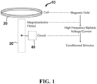
- FIG. 1 a basic schematic diagram illustrates aspects of an apparatus 10 according to the present disclosure.
- exemplary embodiments of the present disclosure can be configured to stimulate neural tissue, power devices that record physiological signals, and/or couple recording and stimulation for closed-loop bioelectronic medicine.
- Apparatus 10 comprises a magnetic field generator 20 (shown in this example as a coil), a magnetoelectric (ME) film 30, and an electrical circuit 40 coupled to a central portion of the film 30. Coupling the circuit to the center of the film is important for maximum efficiency and enables a voltage amplitude that can stimulate cells because it minimizes mechanical damping of the ME film resonance.
- a magnetic field generator 20 shown in this example as a coil
- ME magnetoelectric
- magnetic field generator 20 generates a magnetic field that is converted to a high frequency monophasic or biphasic voltage/current by film 30, which is then converted to a conditioned stimulus by electrical circuit 40.
- Apparatus 10 can be configured to control the amplitude and waveform of the conditioned stimulus to achieve stable and effective neural stimulation.
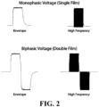
- electrical circuit 40 can be configured to convert the high-frequency magnetic field into any of the following waveforms shown in FIG. 2.
- FIG. 2 illustrates a monophasic, high frequency waveform (e.g. created using a diode), a monophasic, low frequency/envelope waveform (e.g. created using a diode and capacitor), a biphasic, high frequency waveform (e.g. created using a circuit and two films), and a biphasic, low frequency/envelope waveform (created using a circuit and two films, or a circuit and one film).
- a monophasic, high frequency waveform e.g. created using a diode
- a monophasic, low frequency/envelope waveform e.g. created using a diode and capacitor
- a biphasic, high frequency waveform e.g.
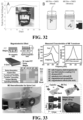
- FIG. 3 examples of different circuits that can be used to generate different waveforms according to the present disclosure.
- the diagrams shown in FIG. 3 are schematic diagrams only, and are not to scale.
- the circuits shown in FIG. 3 are coupled to an end portion of the film(s), while exemplary embodiments include circuits coupled to the central portion of the film.
- the diagrams shown are merely exemplary of the types of circuits that can be utilized to generate the desired waveforms.
- exemplary electrical circuits can comprise rectifiers, diodes, transistors, resistors and other components as needed to produce the desired waveform.
- the piezoelectric film acts as a capacitor with a capacitance value determined by the size and dielectric constant.
- a diode in parallel with the film creates a clamper circuit which biases the high frequency waveform.
- transistors can be added such that circuitry leading to the non-active film is switched off while the active film is providing a signal allowing for the creation of the biphasic waveform.
- Resistors can be used to limit the current or voltage of the waveform applied to the tissue, as well as provide locations to probe the circuit to test functionality.
- An LED or zener diode in parallel with the film and diode can be used to cap the film output voltage at the forward bias voltage of the zener diode or LED.
- a capacitor in parallel with the film can be used the smooth the waveform and create the envelope feature shown in FIG 2 .
- an integrated circuit could also be designed to generate the desired waveform, which could also include capacitors for energy storage.
- the need to create monophasic or biphasic stimulation depends on which condition is being treated. For example, as shown in panel D of FIG. 6 , chronic back pain may be addressed with monophasic stimulation, while Parkinson's may be addressed with biphasic stimulation.
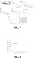
- the voltage output As the device moves with respect to the magnetic field generator (e.g. a fixed amplitude device). It may also be important to adjust the amplitude of the stimulus as the tissue changes, the device migrates over time, or the needs of the patient changes (tunable amplitude).
- the device can operate in fixed amplitude configuration, which can be accomplished by adding an LED or diode in parallel with the first diode.
- the forward bias voltage sets the capping voltage of the device.
- the device can also be operated in a tunable amplitude configuration to condition the amplitude of the stimulus.
- Such configurations can use pulse width modulation to increase or decrease the stimulus amplitude by changing the duration or the frequency of the high-frequency magnetic field pulse.
- Certain embodiments may utilize a frequency shift. For example, by changing the magnetic field frequency slightly away from resonance on a characterized film, one can lower the output voltage. This is useful for applications where the pulse length needs to be long but the amplitude needs to be kept lower.
- Particular embodiments may also use pulse duration control. For example, for very short pulses one can characterize a film and use the rising time constant calculated to determine the number of magnetic field pulses needed to achieve a desired voltage. This can be useful for amplitude control in applications where the pulse time is very short.
- certain embodiments may utilize a programmable function to program the device. For example, data can be sent via the magnetic field to switch between stimulation modes in the electrical circuit as needed.
- the inventors can apply a slowly varying envelope to this high-frequency carrier to stimulate electrically excitable cells.
- the inventors can create a stimulus pulse train at 130 Hz (the typical therapeutic frequency for DBS) by applying a series of brief high-frequency pulses (approximately 1 ms in duration) and using a diode to rectify the ME response.
- Exemplary embodiments can dynamically adjust the voltage produced by the ME device to match traditional DBS stimulation by changing the properties of the magnetic stimulus. For example, by adding a capacitor and resistor in series with the ME film, one can engineer an RC time constant that is fast compared to the desired pulse train (130 Hz), but slow compared to the carrier frequency ( ⁇ 100 kHz). In this case, the duration or duty cycle of the high-frequency magnetic pulse can be adjusted such that the film reaches a voltage determined by the time constant for charging the film.
- System 100 comprises a first a magnetoelectric film 110 and a second a magnetoelectric film 120. It is understood that other embodiments may comprise a single magnetoelectric film.
- System 100 further comprises a magnetic field generator 130 comprising a permanent magnet 132 and an alternating current magnetic coil 134. While the embodiment shown utilizes a permanent magnet in the magnetic field generator, other embodiments may utilize an electromagnet in the magnetic field generator.
- magnetic field generator 130 is configured to generate a magnetic field 136 at a frequency between 20-500 kHz.
- first and second magnetoelectric films 110 and 120 are configured to produce an electrical output signal 146 when stimulated by magnetic field 136 at the input frequency generated by magnetic field generator 130.
- electrical circuit 140 is configured to modify the electrical output signal such that electrical output signal 146 has an output frequency between 0.5-1000 Hz.
- electrical circuit 140 may comprise various components, including for example, one or more rectifiers 142, transistors 144 and resistors 148.
- Electrical output signal 146 can be transmitted through a stereotrode 150 to activate neurons in a biological sample 160 (e.g . brain tissue).
- a biological sample 160 e.g . brain tissue
- magnetoelectric films 110 and 120 can be fabricated through the combination of a piezoelectric layer, Polyvinylidene Fluoride (PVDF) and magnetostrictive layer (e.g . Metglas) to form the magnetoelectric (ME) film.
- PVDF Polyvinylidene Fluoride
- ME magnetoelectric
- the two layers are first plasma treated to promote adhesion and a clean surface. The layers can then be bonded with the application of an approximately 30 ⁇ m thick epoxy layer. Once cured, the composite thin film can be cut using a femtosecond laser system that has can cut devices on the sub-millimeter scale.
- electrical circuit 140 can comprise a novel H-bridge circuit to serve as a magnetic coil driver to reach high voltages and frequencies. It is understood the specific fabrication methods and materials disclosed herein are merely exemplary, and embodiments of the present disclosure are not limited to such methods and materials.
- magnetoelectric films 110 and 120 may be fabricated by spin coating the piezoelectric polymer (PVDF-TrFE), using PZT piezoelectric ceramic material, or using electrospinning and direct writing methods of PVDF nanofibers.
- PVDF-TrFE piezoelectric polymer
- electrospinning and direct writing methods of PVDF nanofibers when the ME film is brought into contact with an alternating magnetic field produced by the driver and a permanent bias magnet or DC bias coils, the film will resonate and generate up to 50V peak-to-peak.
- the appropriate circuitry can be electrically coupled to the film to obtain the desired output voltage waveform, including examples discussed below.
- other magnetostrictive materials may also be utilized, including zinc oxide (ZnO) nanoparticle doped PVDF films.
- ZnO zinc oxide
- PVDF is a piezoelectric polymer that is less piezoelectric than PZT but is a soft conformal material, and it has been shown that ZnO nanoparticles embedded in PVDF enhances its piezoelectric properties, mainly by increasing the dielectric constant of the composite film [48].
- One of the primary challenges for wireless neural stimulators is to create efficient miniature devices ( ⁇ 1 cm in length) that operate reliably beneath bone and tissue as an animal or human patient engages in normal activity. At lengths of less than 1 cm, devices could be fully implanted in the periphery and be light enough to allow for unrestricted animal behavior; however, for devices this small, power delivery remains a challenge. Efficient power transfer with propagating electromagnetic waves requires antennas with feature sizes comparable to the electromagnetic wavelength. Thus, for sub-millimeter devices, such as the proposed RF powered "neurograins [6]," effective power-transfer frequencies lie in the GHz range, where electromagnetic radiation is absorbed by the body [7].
- PD Parkinson's Disease
- epilepsy For neural stimulators to treat a number of neurological disorders like Parkinson's Disease (PD), obsessive-compulsive disorder, and epilepsy, they must operate safely and effectively in the high-frequency "therapeutic band" between 100 and 200 Hz [10-12].
- This type of high-frequency neural stimulation is challenging because charge on the electrode must be dissipated between successive stimulation pulses to prevent electrolysis, tissue damage, and changes to the local pH [13].
- Charge dissipation at high-frequencies is accomplished by using a biphasic stimulus waveform that actively or passively charges and discharges the electrode with each cycle.
- all clinically approved electrical neural stimulation therapies in this therapeutic band use various forms of "charge balanced" biphasic stimulation waveforms [14].
- magnetoelectric (ME) materials enable the first magnetically powered miniature neural stimulators that operate in the therapeutic high- frequency band. Similar to inductive coils, these materials transform a magnetic field to an electric field, but instead of using an implanted coil the inventors use a material that generates a voltage via mechanical coupling between magnetostrictive and piezoelectric layers in a thin film. Namely, the magnetic field generates strain in the magnetostrictive layer as the magnetic dipoles align with the applied field. That strain exerts a force on the piezoelectric layer, which generates a voltage ( FIG. 5 ).
- magnetoelectrics do not suffer from the same miniaturization constraints as coils and can be driven by weak magnetic fields on the order of a few millitesla. These properties have led researchers to propose magnetoelectrics as a promising material for bioelectronic implants [23-27].
- the inventors demonstrate the first proof-of-principle wireless neural stimulators based on ME materials in a freely behaving rodent model for Parkinson's Disease (PD), and that these materials could power miniature devices deep within the human brain.
- PD Parkinson's Disease
- the inventors fabricated proof-of-principle ME stimulators by bonding a rectangular magnetostrictive layer (Metglas) to a platinum coated piezoelectric layer, polyvinyldine fluoride (PVDF). The inventors then encapsulated the films in a protective parylene-C layer (8-10 ⁇ m thick) ( see FIG. 6 . panel (a), see also Methods section).
- PVDF polyvinyldine fluoride
- This embodiment incorporates PVDF layers between 28 and 110 ⁇ m, which yielded total device thicknesses between 50-150 ⁇ m.
- Other embodiments may include alternative or additional piezoelectric materials, including for example, lead zirconate titanate, also referred to as PZT.
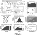
- FIG. 6 provides an overview of how ME films convert alternating magnetic fields into a voltage.
- FIG. 6 panel (a) a diagram of a ME device is shown on a freely moving rat for wireless neural stimulation.
- the active ME element comprises piezoelectric PVDF (blue) and Metglas (gray) laminate encapsulated by Parylene-C.
- the inset shows the operating principle whereby the strain produced when magnetizing the gray magnetostrictive layer is transferred to the blue piezoelectric layer, which creates a voltage across the film.
- FIG. 6 panel (b) an example of a resonant response curve for a ME film shows that the maximum voltage is produced when the magnetic field frequency matches an acoustic resonance at 171 kHz.
- the photograph inset shows an example of an assembled ME stimulator.
- the "Stress profile" inset shows a top view of the stress produced in a ME film as calculated by a finite element simulation on and off resonance (COMSOL).
- FIG. 6 panel (d) shows a maximum stimulation duration (using a 400 ⁇ s/phase pulse repeated at increasing frequencies) for a ME device in biphasic and monophasic operation.
- Dashed lines indicate frequencies of electrical stimulation used in various clinical applications, showing that biphasic operation is necessary for many clinically relevant applications.
- Roman numerals indicate stimulation frequencies demonstrated by previously published miniature magnetic stimulators (i: Magnetothermal, Chen et. al, 2015 , ii: Magnetothermal, Munshi et. al, 2017 , iii: Mid-Field Optogenetics, Montgomery et. al, 2015 , iv: RF Inductive Coupling, Freeman et. al, 2017 ).
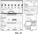
- FIG. 7 illustrates ME properties as a function of film size.
- Panel (a) shows a schematic of experimental setup used to gather data. Testing was performed for ME films with three different PVDF thicknesses: 28 (blue), 52 (red), and 110 (yellow) ⁇ m.
- FIG. 7 panel (b) shows resonant frequency as a function of film length
- panel (c) shows output voltage as a function of film length
- panel (d) shows output voltage as a function of film surface area
- panel (e) shows Q-factor as a function of film length
- FIG. 7 panel (f) shows maximum power output as a function of film width for 52um PVDF thickness
- panel (g) illustrates peak resonant voltage plotted vs. PVDF thickness, showing that the peak ME voltage increases with the PVDF thickness. Error bars indicate +/- 1 standard deviation for n ⁇ 50 films for each thickness.
- FIG. 7 panel (h) shows ME voltage as a function of angle between the film and the coil. Blue region shows the range of operating angles for which the voltage is greater than the expected stimulation voltage.
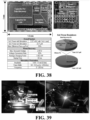
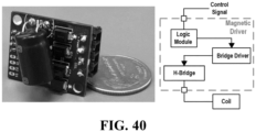
- FIG. 8 shows film output voltage as a function of bias field. The peak resonance voltage is significantly increased by a modest bias field that can be produced by a permanent magnet.
- FIG. 9 shows aspects of a magnetic field driver.
- panel (a) illustrates a schematic of the major components of the magnetic field driver, where the dashed line denotes components rendered in panel (b).
- panel (c) shows an output waveform for monophasic stimulation and the parameters that can be controlled by the drive software, while panel (d) shows an output waveform for biphasic stimulation, and the parameters that can be controlled by the driver software.
- the inventors tested them in saline and found that with a biphasic stimulation waveform the inventors could apply constant stimulation up to at least 800 Hz without significant hydrolysis.
- the inventors operated either one film for monophasic stimulation or two films for biphasic stimulation attached to a stereotrode (Microprobes) in saline (see Methods).
- the inventors then measured the time at which the inventors could see bubbles at the electrode tip resulting from hydrolysis. This hydrolysis event indicates conditions that would lesion the surrounding tissue.
- biphasic ME devices shown here are the first to access the high- frequency bands used for clinical applications like the treatment of Parkinson's disease and obsessive-compulsive disorder (as shown in FIG. 6 panel [d]).
- An additional challenge for any wirelessly powered neural stimulator is to maintain a well-regulated stimulation voltage. This challenge is especially prevalent as devices become small, which often reduces the power transfer efficiency resulting in a greater sensitivity to the alignment between the device and power transmitter.
- ME materials offer two main advantages that can enable stable and effective stimulation even as devices become small and move with respect to the driver coils.
- ME devices generate voltages well in excess of the effective stimulation potential, allowing them to be effective even if the materials are misaligned with the driver coils.
- the inventors have measured ME voltages in excess of 30 V at a field strength of only 1 mT (as shown in FIG. 7 panels [c] and [d]). Because effective stimulation voltages are usually between 1-5 V, the inventors can cap the applied voltage to this effective stimulation range using an LED or Zener diode. As long as the voltage generated by the ME film is greater than or equal to the capping voltage, the inventors will apply approximately the same stimulus voltage regardless of the angle or distance between the driver coil and the ME film.
- the voltage generated by a piezoelectric material depends on the thickness of the piezoelectric layer and not the area of the film [30], allowing the inventors to fabricate small magnetoelectric films that generate roughly the same stimulation voltage as larger devices.
- FIG. 7 shows the peak voltage generated and quality factor for ME films of different areas. The inventors found that, for a 52 ⁇ m thick PVDF layer, the voltage remains around 10 V even as the film length decreases. Variations of +/- 40 % in peak voltage and quality factors are likely due to defects produced during film fabrication, which may be reduced with improved manufacturing.
- the inventors also verified that the output voltage depends only on the piezoelectric film thickness by measuring the peak voltages from ME devices with three different thicknesses of PVDF: 28 ⁇ m, 52 ⁇ m, and 110 ⁇ m. As expected, one can see that the peak voltage increases linearly with the PVDF thickness and is independent of the film length.
- the inventors calculated (and experimentally confirmed) that the power generated by a ME device is proportional to the film width for a given thickness and a length-to-width ratio >3 (see FIG. 7 panel [f]). Despite the decrease in power as films become smaller, the inventors calculate that films less than 1 cm long can generate up to 4 mW, which is more than sufficient for many wireless applications including neural stimulation [31].
- HEK human embryonic kidney
- FIG. 10 aspects of monophasic ME stimulators activating cells in vitro are illustrated.
- FIG. 10 panel (a) shows a schematic of the experimental setup, while panel (b) shows a microscope image of holes stamped into the ME film and finite element simulation of the electric field shows that the holes produce fringing electric fields that overlap the culture cells.
- FIG. 10 panels (c) and (d) show the voltage across the ME film when the magnetic field is on resonance and off resonance, respectively. Insets show an enlarged view of the high frequency carrier waveform.
- FIG. 10 panel (a) shows a schematic of the experimental setup
- panel (b) shows a microscope image of holes stamped into the ME film and finite element simulation of the electric field shows that the holes produce fringing electric fields that overlap the culture cells.
- FIG. 10 panels (c) and (d) show the voltage across the ME film when the magnetic field is on resonance and off resonance, respectively. Insets show an enlarged view of the high frequency carrier waveform.
- FIG. 10 panel (a) shows a schematic of the
- FIG. 11 shows ME stimulation of cells grown directly on ME film.
- FIG. 11 panel (a) shows a schematic of the experimental setup.
- FIG. 11 panel (b) shows a microscope image of fixed cells adherent to the region around a stamped hole (Hoechst/Calcein-AM, cells labeled prior to fixing).
- FIG. 11 panel (c) shows ArcLight fluorescence of spiking HEK cells when magnetic field is on resonance and panel (d) off resonance.
- the inventors coated the top parylene layer with poly-I-lysine.
- the healthy proliferation of HEKs on the ME device indicates that this encapsulation approach prevents the ME materials from limiting cell growth ( FIG. 11 , panel [b]).
- the target cells may not adhere to the ME stimulator, so the inventors also tested the response of cells laid on top of the ME materials. In this configuration the inventors first grew the cells on coverslips for 3-5 days before inverting the coverslips and laying them on the ME for testing ( FIG. 6 , see Methods).
- the films were otherwise fabricated as described herein ( FIG. 6 , Methods).
- high-frequency biphasic stimulation at the ME resonance frequency typically 20-150 kHz
- APs action potentials
- the inventors used a Schottky diode to rectify the voltage to create entirely positive or negative voltage waveforms depending on the diode direction. This rectified waveform has a slowly varying monophasic envelope in the ⁇ 500 Hz frequency band where cells are responsive ( FIG. 10 panels [c] and [d]).
- the inventors found that five stimulation pulses with an envelope frequency of 100 Hz consistently stimulated APs in the spiking HEK cells ( FIG. 10 , panel [e], FIG. 11 , panel [c]). Significantly, this 10-500 Hz stimulation frequency spans the therapeutic window for many deep brain stimulation treatments [34], and is difficult to achieve with other wireless stimulators that compensate for low-efficacy energy harvesting by charging on-board capacitors [35].
- the carrier frequency of the magnetic field was at the resonant frequency of the device, which varied between 20-40 KHz depending on device length. To test stimulation reliability, the inventors repeated the 5-pulse stimulus three times over a period of 30 seconds.
- the inventors also confirmed that the fluorescent signal recorded indeed represents the voltage-dependent ArcLight response by imaging cells transfected with voltage-independent cytoplasmic GFP. These cells showed no change in fluorescence when the films were driven at the resonant frequency ( FIG. 10 panel [g]).
- Biphasic stimulation by ME films evoke action potentials in brain slices
- biphasic stimulation is preferred for most applications due to the desire to create a charge-balanced stimulus that reduces charge buildup and undesired electrochemical reactions at the electrode surface13.
- the voltage waveform produced by ME films at resonance is biphasic, these resonant frequencies (typically 20 - 150 kHz) are too high to produce reliable cell stimulation, as described above.
- the inventors use two films with distinct resonant frequencies connected to the same stimulating electrodes ( FIG. 12 panel [a]). The first film is attached to a full wave rectifier, which is oriented to generate a positive pulse, while the second film is attached to a full wave rectifier that generates a negative pulse.
- the transistors block currents generated by one film from propagating through the circuitry attached to the other film, ensuring that only one half of the circuit is active at a time.
- the inventors can alternate positive and negative phase stimulation to create a biphasic neural stimulator ( FIG. 12 , panels [b-d]).
- the residual charge of -2.3 nC, which discharges in ⁇ 2 ms, implies that this stimulator can safely operate at frequencies up to >500 Hz without accumulating charge.
- the biphasic ME stimulator is capable of repeatable neural stimulation using neocortical brain slices derived from mice that express the genetically encoded calcium indicator GCaMP3 in GABAergic neurons.
- To image neural activity following ME stimulation the inventors inserted a stereotrode attached biphasic ME stimulator described above while the inventors imaged GCaMP activity using fluorescence microscopy ( FIG. 12 , panels [e-g], Methods).
- the inventors chose neural stimulation parameters similar to those commonly used for deep brain stimulation [34]: 100 biphasic pulses at 200 Hz with each phase lasting 175 ⁇ s.
- FIG. 12 illustrates aspects of biphasic ME stimulators activating neurons in ex vivo brain slices.
- FIG. 12 panel (a) shows a schematic of experimental setup with two ME films for biphasic stimulation. This setup is similar to the embodiment described in FIG. 1 , but includes a microscope objective for observation.
- FIG. 12 panel (b) shows a measured voltage waveform produced by the magnetic field generator. When coupled to the magnetic coils, this waveform produces magnetic fields that alternate between the resonant frequencies of the two ME films.
- FIG. 12 panel (c) shows measured voltage across the stereotrode, which shows the expected biphasic pulse shape.
- FIG. 12 panel (d) shows the calculated current based on measuring the voltage across our load resistor (VR) shows nearly perfect charge balancing with only 2.3 nC accumulating on the electrode per pulse train.
- FIG. 12 panel (f) shows the average GCaMP signal when resonant magnetic field is applied before (panel [f]) and after (panel [g]) adding TTX shows neural activity is induced by the ME stimulator. Thin green traces represent separate experiments from two different brain slices, and thick black traces represent the mean of all experiments.
- a major advantage of the ME stimulators disclosed herein is the fact that remote activation enables experiments with freely behaving animals.
- the inventors adapted the biphasic stimulator for deep brain stimulation (DBS) in freely moving rats, as shown in FIG. 13 .
- DBS deep brain stimulation
- the inventors used a previously reported protocol to test DBS in hemi-parkinsonian rats [36].
- rats are injected with 6-OHDA in the left medial forebrain bundle (MFB) to create a unilateral lesion of the substantia nigra pars compacta (SNc).
- MFB left medial forebrain bundle
- SNc substantia nigra pars compacta
- the hemi-parkinsonian rats Following a dose of methamphetamine, the hemi-parkinsonian rats have been shown to rotate ipsilateral to the injection (e.g. left for injection into the left MFB). During these rotations, the rat primarily moves using its contralateral (right) forepaw, rarely placing the ipsilateral (left) forepaw onto the ground.
- a biphasic stimulus is applied at 200 Hz in the sub-thalamic nucleus (STN) using a tethered electrode array stimulator
- rats typically stop turning to the left and exhibit more normal behavior such as moving with both forepaws, maintaining a steady orientation, or turning to the contralateral side [34].
- the inventors To create a wireless, biphasic ME stimulator for freely moving animals the inventors added a small permanent magnet to the ME stimulator to generate a bias field, and wrapped the behavioral chamber with 18 AWG copper wire to create a solenoid ( FIG. 13 panel [a], FIG. 14 ).
- the small permanent magnet ⁇ 0.25g
- the inventors could ensure that the bias field was constantly aligned with ME films as the animal moved within the enclosure.
- the inventors could also ensure that the positive and negative stimuli had equal amplitudes by independently adjusting the distance between each film and the permanent magnet.
- This ME stimulator was then connected to a commercial electrode array (Microprobes) implanted in the STN ( FIG. 13 panel [b], Methods).
- the inventors ensured that the stimulation voltage and current were within the safe and therapeutic range by measuring the output of the ME stimulator connected to an equivalent circuit model of the brain ( FIG. 13 panel [c], Methods). Specifically, the inventors observed peak voltages of approximately +/-1.5 V and peak currents of approximately +/- 100 ⁇ A for 400 us at approximately a 50% duty cycle (200 ⁇ s of overall current per phase), which is within the effective stimulation range reported for conventional wired stimulators [36]. When the inventors tune the magnetic field frequency off resonance they observe almost no generated voltage or current ( FIG. 13 , panel [c]).
- FIG. 13 effective DBS is shown in a freely moving rat using a wireless ME stimulator.
- FIG. 13 panel (a) illustrates an experimental setup showing rat in a circular enclosure wrapped with magnet wire. The inset shows a biphasic ME stimulator on a one cent coin.
- FIG. 13 panel (b) shows a schematic of the biphasic ME stimulator attached to the electrode array that is implanted into the STN.
- FIG. 13 panel (c) shows measured voltage generated by the ME device and the current applied to the brain on resonance (green) and off resonance (blue). Approximately 100 ⁇ A biphasic stimulation is applied only when then the magnetic field frequency matches the resonance condition.
- FIG. 13 panel (a) illustrates an experimental setup showing rat in a circular enclosure wrapped with magnet wire. The inset shows a biphasic ME stimulator on a one cent coin.
- FIG. 13 panel (b) shows a schematic of the biphasic ME stimulator attached to the electrode array that is implanted into the STN.
- FIG. 13 panel (d) shows the angular velocity of the hemi-Parkinsonian rat over a 40-minute DBS trial with intervals of resonant and non-resonant stimulation shows that rotations are reduced only when the stimulator is activated by a resonant magnetic field.
- FIG. 14 panel (a) illustrates a schematic showing the location and spacing of wires and the number of drivers used to generate the alternating magnetic field overlaying a COMSOL simulation of magnetic field strength in the chamber
- FIG. 15 illustrates ME devices can operate several centimeters above a single magnetic coil.
- FIG. 15 panel (a) shows a COMSOL simulation of magnetic field above a circular coil
- FIG. 15 panel (b) shows the measured device output voltage as a function of distance above the coil.
- FIG. 16 shows the predicted depth that various miniature antennas could be safely implanted under the skull and generate 1 mW of power, which is in the approximate maximum power required for high-frequency continuous neural stimulation [31].
- radio-frequency (RF) powered antennas that operate at frequencies above ⁇ 1 MHz have limitations in the amount of power that can safely be delivered to an implanted device without causing potentially harmful tissue heating.
- FIG. 16 illustrates aspects of a miniaturized multichannel stimulation in a human skull phantom.
- FIG. 16 panel (a) shows a comparison of effective depth beneath a human skull phantom for ME devices compared to other miniature wireless stimulators. The depth limit is based on safety limits to generate 1 mW. (i: Park et. al, Proc Nat Ac Sci, 2016 , ii: Yazdandoost et. al, Asia Pac Microw Conf, 2009 , iii: Yazdandoost et. al, Proc 37 Europ Microw Conf, 2007 , iv: Agrawal et. al, Nat Biomed Eng, 2017 ).
- FIG. 16 panel (b) shows photos of ME films next to a grain of rice and the corresponding voltage as a function of magnetic field frequency (field strength 1 mT, scale bars 2 mm).
- FIG. 16 panel (c) is a schematic showing potential application of fully implanted ME films with the magnetic field generated by an external coil that can be incorporated into a hat or visor.
- FIG. 16 panel (d) shows a front view and panel (e) a top view of skull phantom with the top removed to view LEDs (film locations indicated by arrows, scale bar 1 cm).
- FIG. 16 panel (f) shows a photo of LEDs attached to ME films with the magnetic fields at applied at180 kHz and
- FIG. 16 panel (g) shows 200 kHz. Selective illumination of the LEDs corresponding the resonant frequencies of the films demonstrates successful multichannel activation of individual films (scale bars 1 cm). Magnetic field strength was measured to be 0.5 mT at the location of the ME films.
- two rice-sized ME films can be individually addressed at the center of a human skull phantom using an external electromagnet.
- These two-films with lengths of 8 mm and 10 mm have acoustic resonant frequencies of 180 and 200 kHz, which are determined by the film length.
- their output voltage is capped at approximately 1.8 V, which helps to regulate the stimulation voltage and allows us to visualize film activation.
- ME films of this size are smaller than current DBS leads and could potentially be implanted into deep brain areas as shown in FIG. 16 panel (c). Additionally, the magnetic stimulation coil is small enough to be incorporated into a stylish hat or visor that could be worn comfortably by a patient.
- the inventors placed the two ME films at the center of a skull phantom, they found that they could individually illuminate the LEDs on each film when they applied a magnetic field at the resonant frequency of the selected film ( FIG. 16 panels [d-g]).
- the inventors used a 400 W power supply, which produced a field of approximately 0.5 mT at the center of the skull phantom.
- the top of the skull phantom was removed for visualization, but had no effect on our ability to drive the LED indicators.
- the number of stimulation channels could be increased with the addition of ME films with different resonant frequencies.
- ME stimulators such as the example described in the in vivo rat experiment could have an immediate impact on the study of DBS therapies using rodent disease models. Because the ME stimulator is compatible with commercial implanted electrodes, and the magnetic stimulators can be adapted to a number of standard behavioral experiments or animal enclosures, the ME stimulators disclosed herein could readily replace the wired DBS stimulators currently in use. As a result, new experiments can be developed to probe the effects of chronic and continuous DBS or DBS in social contexts where wired DBS stimulators would be impracticable.
- ME materials have the potential to enable miniature neural stimulators that can be implanted deep in the brain of large animals or humans and addressed externally with a small electromagnet.
- the inventors also foresee applications for ME materials as a wireless power technology for more complex implantable bioelectronic devices.
- the demonstrated ability of ME films to power LEDs implies that ME materials could power implantable optogenetic stimulators, or small integrated circuits for physiological monitoring.
- ME materials have the potential to fill a key need for wireless power delivery to miniature biphasic neural stimulators and other bioelectronic devices where the major challenge is transferring energy over distances of several centimeters without heating the tissue or suffering loss at interfaces between tissue, bone, and air.
- the inventors used Metglas SA1 alloy (Metglas Inc) for the magnetostrictive layer and polyvinylidene fluoride "PVDF" (precision acoustics) for the piezoelectric layer.
- the PVDF films used for these experiments were pre- stretched and poled by the manufacturer.
- the two layers were bonded together using an epoxy capable of transferring the mechanical stress between the two layers (Hardman double bubble red epoxy).
- the inventors Prior to bonding the two layers together, the inventors sputtered a thin layer of platinum ( ⁇ 100 nm) as a top electrode on the PVDF. Both the Metglas and PVDF were plasma cleaned using O 2 plasma for five minutes before epoxying.
- the films were cut into the desired rectangular shape using scissors, taking care to cut the long axis of the film along the stretching direction of the PVDF.
- the inventors then attached wires using conductive epoxy to either side of the films in order to measure the electrical capabilities of the film.
- the inventors found that attaching wires in the center dramatically increased the resonant voltage.
- the wires were attached near the ends of the films during the in vitro experiments.
- the inventors also attached additional electronic components such as diodes or LEDs to the wires attached to the films as noted in the appropriate sections in the main text.
- the devices were coated in 5-10 ⁇ m of parylene-C (Labcoater 2). Initially this coating was used to electrically insulate and protect the devices during in vitro experiments, but the inventors also found that the encapsulation increases the resonant voltage, which could be due to increased mechanical coupling from the encapsulation.
- the stimulator shown in FIG. 13 panel (a) was wired to a stereotrode immersed in saline under a microscope in order to observe the formation of bubbles from electrolysis at the tips.
- the inventors used only one resonant frequency and during biphasic stimulation the inventors used two frequencies as demonstrated above.
- the pulse time was a 400 ⁇ s/phase.
- the inventors determined the limit of stimulation time as when the first bubble began to appear at the tips of the electrode and repeated each data point 4 times.
- each magnetic field generator comprises two major components: (1) Magnetic coils used for the alternating magnetic field (described in the main text and optimized for each experiment) and (2) Electronic drivers to control voltage and timing of the alternating current in the coils (the same for all experiments).
- the drivers are designed to deliver high currents to the drive coils in the form of bi-phasic pulse trains. This reduces the cost and complexity of the driver itself, as well as the power supply and control circuitry when compared to arbitrary function generators.
- the design also has potential for improved operational efficiency through impedance matching with the drive coils.
- the output carrier and pulse frequencies of the magnetic field are generated using a TeensyLC board and custom chicken code to generate the specific pulse timings to deliver controlled ME stimulation ( FIG. 9 , panels [c] and [d]).
- the setup used to generate the alternating field in the in vivo rotation experiments comprised four sets of coils each with five turns powered by one driver with all four drivers synced to the same output signal. In this way the inventors can generate sufficient power to generate a mT-scale magnetic fields over the whole behavioral area ( FIG. 14 panel (a)].
- HEK cells expressing sodium channel Na 1.3 and potassium channel K 2.1 were grown on 12 mm poly-I-lysine coated coverslips to approximately 30% confluency. The cells were then transfected with the genetically encoded voltage indicator ArcLight using Lipofectamine (Invitrogen) following manufacturer's recommendations. Two to three days after transfection the coverslips were inverted onto ME films for testing. Preparation of GFP controls followed the same procedure with the exception of replacing the ArcLight vector (AddGene) with a GFP expression vector (AddGene). For experiments performed with cells grown on the films, HEK cells transfected with ArcLight were placed onto parylene coated poly-I-lysine treated films. The films were placed in cellular media overnight and tested the following day.
- ArcLight and GFP were excited at 460 nm with an LED light source. Fluorescence images were collected at 33 fps using a CCD camera. Images were analyzed using Matlab to quantify fluorescence changes in individual cells. In vitro testing was performed in extracellular buffer (ECB, in mM: NaCl 119, KCl 5, Hepes 10, CaCl2 2, 671 MgCl2 1; pH 7.2; 320mOsm).
- FIG. 11 panel (b) was obtained by growing unmodified HEK cells on a film submerged in cellular media for five days. The cells were then stained with Hoechst and Calcein-AM to label the nucleus and membrane respectively in living cells. The cells were then fixed and imaged using a confocal microscope.
- the inventors used 40-day old GAD2-GCaMP3 mice, generated by crossing GAD2-Cre (JAX # 10802) with flox-GCaMP3 (JAX # 14538) animals. Preparation of brain slices followed procedures described by Ting et al.45 and was carried out in accordance with National Institutes of Health guidelines and approved by the UTHealth animal welfare committee.
- mice were deeply anesthetized with Isoflurane and perfused with ice cold NMDG-based solution comprising (in mM): 92 NMDG, 2.5 KCl, 1.25 NaH2PO4, 10 MgSO4, 0.5 CaCl2, 30 NaHCO3, 20 glucose, 20 HEPES, 2 thiouera, 5 Na- Ascorbate, 3 Na-pyruvate, saturated with 95% O2 and 5% CO2., at a rate of ⁇ 6 ml/min.
- Coronal brain slices (300 ⁇ m) were cut using a vibratome (Leica VT1200S), incubated for 15 min at 35 °C in NMDG solution, and then transferred to a chamber held at room temperature containing (in mM): 92 NaCl, 2.5 KCl, 1.25 NaH2PO4, 2 MgSO4, 2 CaCl2, 30 NaHCO3, 25 glucose, 20 HEPES, 2 thiouera, 5 Na-Ascorbate, 3 Na-pyruvate, saturated with 95% O2 and 5% CO2.
- slices were placed into a recording chamber perfused with ACSF containing (in mM): 126 NaCl, 2.5 KCl, 1.25 NaH2PO4, 2 MgCl2, 2 CaCl2, 26 NaHCO3, 10 glucose), held at 32-34 °C using a 695 inline heater.
- NBQX (10 ⁇ M) was included in the bath solution to block AMPA receptor-mediated synaptic transmission.
- the stereotrode was placed in layer 5 of somatosensory (barrel) cortex.
- GCaMP3 was excited at 460 nm with an LED light source. Fluorescence images were collected at 9.8 fps using a CCD camera attached to an Olympus BX51WI microscope. Images were analyzed using Matlab to quantify fluorescence changes in 600 ⁇ 600 ⁇ m regions around the stereotrode tips.
- Two male Long-Evans rats (n ⁇ 1, 400 g) were anesthetized with isoflurane gas. Five percent isoflurane was used to induce anesthesia and two percent was used to maintain anesthetic depth. Buprenorphine (0.04 mg/kg) was administered 30 minutes prior to ear bars for analgesia. 5 - 7 skull screws were placed to anchor the electrode array. Skull screws were bound to skull with Metabond dental acrylic. A craniotomy was made to accommodate the micro electrode array and expose an injection site for neurotoxin. A 30-gauge needle bent at the tip cut and pulled away the dura mater covering of the brain.
- Desipramine reconstituted in saline at a concentration of 15 mg/mL was injected IP to protect noradrenergnic neurons.
- the dose of DMI was approximately 15 mg/kg and injected approximately 30 minutes prior to administration of neurotoxin.
- 8 ug of 6-hydroxydopamine (OHDA) at 2 ⁇ g/ ⁇ L in saline was injected at 0.2 uL/min into the mid forebrain bundle (MFB -1.2 ML, -4 AP, and -8.1 DV).
- OHDA 6-hydroxydopamine
- STN stimulation was delivered via a 2x2 platinum iridium microelectrode array (Microprobes) with 600 ⁇ 600 ⁇ m spacing of 75 ⁇ m electrodes. Each electrode had a nominal 10 kOhm impedance. The electrode array was lowered to -2.6 ML, -3.6 AP, and approximately -8.2 DV from bregma. The array was fixed to the skull with dental acrylic. All experiments were approved by the Institutional Animal Care and Use Committee of Rice University.
- the stimulator power was estimated via a benchtop approximation of the rodent electrode impedance.
- Constant current stimulation of the rodent brain with an A-M Systems 4100 stimulator produced characteristic voltage waveforms that approximated a simplified parallel RC circuit.
- a 56 kOhm resistor, and 440 pF capacitor in parallel closely approximated the impedance characteristics of the rat brain across the stimulating electrodes.
- the inventors estimated the field strengths and pulse durations necessary to produce the desired stimulation effects and confirm that the stimulation was charge balanced prior to rodent experimentation.
- the rat Prior to performing the rotation tests the rat was briefly anesthetized with 5% isoflurane gas and injected intraperitoneally (IP) with methamphetamine (0.31 ml 1.25 mg/kg) and the wireless biphasic stimulator was plugged into the implanted electrode array. After the anesthesia had worn off (about 5-10 min) the rat was placed in the cylindrical behavioral chamber. The magnetic field was applied over the whole behavioral area to the films on the device ( FIG. 14 panel [a]).
- IP intraperitoneally
- the magnetic field was applied on resonance and off resonance for one minute at various times during the 40-minute trial.
- the resonant frequencies were 73 kHz and 747 77 kHz and the off resonant frequencies were 63 kHz and 87 kHz.
- Head position on the rotation task was generated using a slightly modified version of DeepLabCut [46] to track ears, snout, and implant.
- a dataset totaling 286 frames from both the on and off resonance rotation tasks was hand labeled and trained for approximately 140,000 iterations.
- certain embodiments may include zinc oxide (ZnO) nanoparticle doped films.
- ZnO zinc oxide
- FIG. 17 a graph illustrates voltage over time for a ZnO nanoparticle doped PVDF/Metglas film that is approximately 8 ⁇ m resonating at approximately 70 kHz. When deviating from the resonant frequency, the voltage drops down to zero.
- PVDF-TrFE a modified PVDF molecule less sensitive to temperature, is dissolved in the solvents methyl ethyl ketone and butanone at 20% w.t. % [49].
- the ZnO nanoparticles (approximately 13 nm in diameter) were added at approximately 10% weight fraction to the solution, and the solution was placed into a bath sonicator for more than 6 hours.
- the solution was then spun coat twice onto a 3 ⁇ 3 cm piece of Metglas at approximately 3000 RPM for 45 seconds yielding a film thickness of approximately 8 ⁇ m.
- the laminate was then thermally annealed at 150 C and electrically poled in the custom-built Corona Poling Setup. This led to one batch of films out of 4 that had higher voltages and self-rectification properties. (see FIG. 17 ).
- Challenges included the reproducibility of the results, where ZnO nanoparticles were insoluble in the PVDF solution especially at higher weight percentages. To the inventors' knowledge, there does not exist evidence in the literature showing self-rectifying behavior of PVDF-TrFE mixed with nanoparticles.
- PVDF-ZnO nanowire materials that reliably demonstrate self-rectification behavior are known [50]. As the ZnO nanowires are grown in situ, it acts as a self-adjustment diode to control the output of the hybrid material.
- the concentration of PVDF in solvents will remain the same (20% w.t. in MEK and Butanone).
- certain embodiments may grow ZnO nanowires from ZnO nano-seeds.
- Potential embodiments may use Zn(Ac2) (Zinc Acetate) as the seeds and mix it with PVDF solution.
- the hybrid solution can also then be spun coated onto a Metglas substrate.
- the thin film can be placed into an aqueous solution of ZnNO3 (Zinc Nitrate) and nanowires are naturally grown at 80C for 6 hours.
- ZnNO3 Zinc Nitrate
- the timing and termination of reaction will depend on the size of nanowires that are desired.
- the PVDF is naturally stressed due an extension force by ZnO NW growth, the PVDF material is naturally formed into the piezoelectric beta phase.
- the inventors can also electrically pole the material with a corona poling setup. The final product will be probed to test with microwires and measure voltages at resonant frequencies.
- FIG. 18 illustrates x-ray diffraction data showing the poling of PVDF with alpha and beta phase peaks of PVDF, which can be used to verify films post ZnO nanowire growth.
- FIG. 19 illustrates aspects of ZnO/PVDF film fabrication.
- Panel (a) of FIG. 19 shows the incorporation of zinc acetate into PVDF solution to serve as nanoseeds, which form a film and grow nanowires in zinc nitrate.
- Panel (b) shows a scanning electron microscope (SEM) image of ZnO nanowire grown in PVDF.
- Panel (c) shows an SEM image of ZnO nanowire on the surface of the PVDF, while panel (d) of FIG. 19 shows a close-up view of the ZnO nanowires.
- SEM scanning electron microscope
- FIG. 20 illustrates self-rectification of current for a PVDF/ZnO nanowire hybrid material used as an energy harvester when a finger presses on the material.
- an apparatus 200 comprises an implantable wireless neural stimulator 210 and a magnetic field generator 220 configured to generate a magnetic field 236 at one or more input frequencies.
- implantable wireless neural stimulator 215 comprises a magnetoelectric film 230, a charge storage element 235, an electrical circuit 240, a first electrode 251, and a second electrode 252.
- electrical circuit 240 is coupled to magnetoelectric film 230 via first and second electrodes 231 and 232.
- Exemplary embodiments of the present disclosure may sometimes be referred to herein as "Mag-Dust" or "MagMote” devices.
- magnetoelectric film 230 is configured to produce an electrical signal 245 when magnetoelectric film 230 is stimulated by the magnetic field at a particular input frequency.
- Electrical circuit 240 can be configured to modify electric signal 245 to charge the charge storage element 235, which in particular embodiments may be a capacitor.
- electrical circuit 240 can be configured to transmit data to components of implantable wireless neural stimulator 210 and can be configured to provide a stimulation output 258 to third electrode 251 and fourth electrode 252.
- stimulation output 258 can be used to stimulate nerve tissue 290, and in particular embodiments third electrode 251 and fourth electrode 252 may be configured as a stereotrode.
- electrical circuit 240 comprises charging module 241 configured to provide power management and charging of charge storage element 235.
- the illustrated embodiment of electrical circuit 240 comprises a data module 242 configured to provide data transfer and control.
- the embodiment of electrical circuit 240 shown in FIG. 22A also comprises a stimulation driver module 243 configured to provide stimulation output 258 to third electrode 251 and fourth electrode 252.
- charging module 241 comprises a rectifier, a reference generator, a low dropout (LDO) linear voltage regulator, and a power-on-reset (POR).
- the illustrated stimulation driver module comprises a reference current generator and a current digital-to-analog (DAC) converter.
- the illustrated data module comprises a control signal generator, a stimulation controller, and a clock recovery module.
- FIG. 22B illustrates circuit diagrams for specific embodiments of the rectifier, the native MOS-based voltage reference, and the 5-bit programmable stimulation driver. Additional discussion of operational aspects of electrical circuit 240 and specific components is provided below in the section entitled "Example” below.
- electrical circuit 240 comprises a complementary metal-oxide-semiconductor (CMOS) chip 247 that can interface with a ME transducer 239 incorporating magnetoelectric film 230 to receive power and commands (e.g . through data transfer), and drive programmable electrical stimulation.
- CMOS complementary metal-oxide-semiconductor
- AC voltage induced on magnetoelectric film 230 is first converted to a DC voltage with an efficient active rectifier driven by 4-input differential comparators. The energy can be temporarily stored in charge storage element 235 for the next stimulation phase.
- a low-dropout regulator will provide a stable 1V supply to the rest of the system (except stimulation), to reduce their power consumption and effectively increase the load impedance of the application-specific integrated circuit (ASIC).
- ASIC application-specific integrated circuit
- the ASIC can cycle through a charging step 261, a data receiving step 262, and a stimulation step 263.
- downlink data transfer will be performed with amplitude shift keying (ASK) modulation of the magnetic field (shown in FIGS. 21 and 22A ).
- Received data can be used to program system operation and stimulation modes.
- An integrated stimulation driver can be used to drive electrodes 251 and 252 (shown in FIGS. 21-22 ) with current-regulated biphasic pulses, covering a wide range of therapeutic-relevant stimulation patterns (e.g . 0-200 Hz frequency, 30-1500 ⁇ A amplitude, and 50-500 ⁇ s pulse width).
- One challenge to the ASIC design is to maintain reliable operation when the amplitude of voltage induced on ME transducer 239 varies under different distance and angle between the ME transducer 239 and magnetic field generator 220.
- Exemplary embodiments can address this by maximizing the power conversion efficiency of the device, and making the system adaptive to environmental conditions, controllable by external transmitters, and calibration-free. These properties may be achieved with three circuit and system features: (1) optimized power interface to the ME transducer with different materials; (2) an adaptive ME-based data receiver to reliably initiate data transfer and decode data, even when the ME- induced voltage changes; and (3) low-power and calibration-free circuits to minimize the ASIC's quiescent power and maximize the energy available for stimulation.
- Enhancing the power conversion efficiency of Mag- Dusts to extract more usable power from a low-strength magnetic field is critical in realizing our aims on, (1) reliable operation under large physical distance and angle variations, and (2) wearable battery-powered transmitters.
- no battery will be integrated into the Mag-Dusts, which will be continuously powered by the external magnetic field.
- all harvested energy will be used for stimulation and system operation or wasted.
- it will be more efficient to extract a high voltage directly from the ME transducers than pursuing the maximum power point with a low-efficiency DC-DC up-converter as in most ambient energy harvesters.
- the inventors will study ME transducer's electrical model, Mag-Dusts' power management, and impedance matching between ME transducers and ASICs.
- Electroelectric laminate composites can be modeled with an RLC model shown in FIG. 24 panel (a). This model can be calibrated with COMSOL physical simulations and measurements of nanofabricated samples.
- FIG. 23 panels (b) and (c) a ME transducer nanofabricated with PZT piezoelectric materials induces a peak voltage at the mechanical resonant 240 kHz, and two purely resistive effective electrical resonant frequencies. It should be noted that some ME materials (like PZT) show purely resistive impedance at resonance, similar to ultrasound transducers [10], while others (like PVDF) are capacitive around resonance.
- the maximum load power e.g . the stimulation phase in most cases
- the effective recharging power to charge storage element 235 shown in FIGS. 21-22 .
- available power stored on the charge storage element actually increases with the received voltage.
- Preliminary simulation results (based on the ME model in FIG. 24 ) confirm this behavior and imply the importance of reducing ASIC's effective load impedance by reducing its quiescent power, as shown in FIG. 25 panel (a).
- the effective load impedance of the ASIC can be as large as tens of kiloohms in certain embodiments.
- the inventors will explore the principle of emulating inductors with multi-phase flipping capacitors [41] for impedance compensation.
- the inventors will investigate its circuit implementation for PVDF-based embodiments, and the reduction of required on-chip capacitance by adding more phases and exploring new switched capacitor topologies.
- Amplitude shift keying is suitable for low-power data communication to implanted devices when high data rate is not required. Because the large inductor necessary for mT-strength magnetic field generators prevents fast switching between different amplitudes, certain embodiments may indirectly modulate the voltage induced on ME transducers by modulating the AC magnetic field's frequency. However, adopting this amplitude modulation scheme presents three challenges: (1) the large energy storage capacitor limiting the switching speed of rectified DC voltage; (2) varying resonant frequencies and voltage conversion efficiencies of ME transducers due to fabrication variations; and (3) unpredictable ME-induced AC amplitude dependent on physical conditions, such as the distance and alignment between the ME transducer and transmitter.
- exemplary embodiments may employ a dual-path structure, one for power delivery and one for data receiving.
- the inventors propose to control the switching be- tween the two paths with a watchdog logic, which monitors changes in ME-induced voltage.
- the transmitter is designed to reduce the average amplitude of ME-induced voltage during data transmission.
- exemplary embodiments will leverage the existing comparator in the active rectifier as a zero-overhead mode-switching watchdog.
- the comparator can generate a train of narrow pulses when the input's amplitude is lower than the voltage stored on the energy capacitor.
- Exemplary embodiments can extract the envelop of this pulse train as the enable signal for data transmission, as shown in FIG. 26 panel (b).
- the external transmitter e.g . magnetic field generator 220 shown in FIGS. 21 and 22
- the external transmitter will have control of the durations of charging and data transmission steps.
- exemplary embodiments can include a simple yet effective method to extract both clock and threshold voltage from the external AC magnetic field.
- the clock can be extracted directly from the frequency of the AC magnetic field, so that the frequency of the recovered clock will be exactly same as that of the transmitter.
- Exemplary embodiments can also extract the threshold voltage from a toggling pilot tone sent by the transmitter before each data transmission session. As a result, the threshold voltage can be placed at 50% of the actual received amplitude in runtime, which is otherwise unknown to the system.
- the received pilot signal can first be low-pass filtered to extract its DC component, and then sampled by a track-and-hold circuit as the final threshold voltage for data decoding, as shown in FIG. 26 , panel (b). Simulated operation of the adaptive data reception scheme is shown in FIG. 27 .
- Exemplary embodiments of the present disclosure may also include low-power and calibration-free voltage references for power management circuits, current references for stimulation driver, and accurate timing control of stimulation.
- reducing quiescent power of exemplary embodiments' ASIC is important to increasing the usable power under a certain magnetic field.
- calibration-free circuits are desired to reduce deploying complexity and improve robustness to environmental variations. Outcomes from this task will primarily be designed for exemplary embodiments' ASIC, but the techniques may be applicable to other low-power applications as well.
- FIG. 28 illustrates low-power CMOS circuit components.
- panels (a-b) calibration-free voltage/current references are shown.
- Panel (c) shows measurement results across fabrication variations, while panel (d) shows a programmable stimulation driver, and panel (e) shows a Wheatstone bridge-based timing reference.
- exemplary embodiments may leverage a logic finite state machine with the clock recovered from AC magnetic field, to control a current digital-to-analog converter and a H-Bridge output driving stage, as shown in FIG. 28 panel (d). It is expected the stimulation pulse width and frequency can be digitally adjusted to the desired value, even under variations of the ME transducer's resonant frequency. However, should the accuracy of stimulation timing control be proven insufficient, exemplary embodiments may leverage CMOS RC oscillators, rather than bulky crystal oscillators, to provide a timing reference without increasing the implant's volume and weight. As shown in FIG.
- exemplary embodiments of the neural stimulator will demonstrate wireless power and data transfer through AC magnetic fields, efficient interface between ME transducers and CMOS ASICs, and fully untethered control of stimulation.
- Exemplary embodiments of the system can comprise a nanofabricated ME transducer, a CMOS ASIC, a ceramic capacitor for temporary energy storage, and a pair of electrodes (on a flexible PCB).
- FIG. 30 panel (a) shows an exploded view of an exemplary embodiment, while FIG. 30 panel (b) illustrates an assembled view of the same embodiment.
- the components will be integrated on a polyimide-based flexible printed circuit board and fully encapsulated.
- the transducers and ASICs can be encapsulated in a way that preserves their mechanical resonance and electrical properties in ionic solutions (like those inside the body).
- Parylene-C is commonly used as a passivation layer for implanted electronics due to its chemical inertness and ability to serve as a strong ion barrier.
- failure of the parylene layer often occurs due to moisture diffusion.
- exemplary embodiments may also be fabricated using atomic layer deposition to deposit aluminum oxide, which is an excellent moisture barrier.
- the bilayer film uses chemical vapor and atomic layer deposition, where both steps are conformal processes that allow for the ME films to be uniformly coated.
- the film will first be encapsulated with a soft material to preserve the mechanical resonance before being enveloped in a hard material.
- a soft material to preserve the mechanical resonance before being enveloped in a hard material.
- the external components, integrated circuit and capacitor will be potted in medical grade epoxy, a material that is regularly used for such applications [46-52].
- exemplary embodiments will test chip and system functionality using a wired PCB in solution test to probe test points before testing a wireless version of the device.
- An advantage for exemplary ME films as a wireless stimulator is that the magnetic field re- quired to activate these devices requires very little power in comparison to other similar wireless power delivery technologies.
- the inventors have been able to successfully activate films with magnetic fields that are less than 1 mT in strength, at least an order of magnitude smaller than other magnetically driven neurostimulation techniques [16].
- the inventors expect to power the Mag-Dust by small lightweight magnetic field generators. These magnetic field drivers will also be used to transmit data to the Mag-Dust ASIC ( see section entitled "Adaptive Data Reception").
- Exemplary embodiments can include a wearable power and data transmitter comprising a battery, a microcontroller, and a H- bridge driver located externally in a wearable pack.
- a wire will run from the pack to the transmitting coil located at the site of the implant.
- a coil can be placed near the back for a spinal cord implant, in a neck band for a Vagus nerve implant, or in a visor around the head for a brain implant, as shown in FIG. 31 panels (a)-(c).
- exemplary embodiments can create a 1 mT field with only 0.2 mA draw on the battery as shown in FIG. 31 panel (d). Using a 1200 mAh battery weighing less than 120 g, battery life is estimated at more than 10 hours if operating continuously at maximum power.
- Downlink data transfer to the ASIC can be accomplished by modulating the frequency of the driver between resonance and off-resonance frequencies. While at full resonance, the input voltage to the IC will be at its maximum. By selecting two alternative driver frequencies slightly off resonance, the IC will detect the changes in voltage developed by the film as information bits, "0" and °1". In exemplary embodiments, circuitry in the IC dynamically tracks these levels to compensate for coupling fluctuations and driver amplitude drift allowing it to robustly interpret the voltage shifts as incoming data.
- the driver's frequency generator can simultaneously generate all three frequencies so that switching between frequencies can be accomplished seamlessly between stimulation pulses, minimizing dead time and maximizing data transmission rate. Accuracy of the frequency generation allows this approach to work reliably, even when the coil and film are designed to have high Q factors to maximize efficiency.
- the functionality of exemplary embodiments can be tested with ME-based wireless power and data transfer by affixing an LED to the stimulation drivers and monitoring the optical signal using a camera or bonded optical fiber ( see FIG. 32 ).
- This can allow remote sensing of the IC's response to power and programming without interaction with the magnetic field driving the device.
- the inventors can verify both the reliability of our programming approach and the effective efficiency of the system across a myriad of testing conditions.
- a testing apparatus can be employed to examine the impact of distance and alignment between coil and device on performance and reliability. Such testing can be performed at 37 degrees Celsius in phosphate buffer solution to approximate the biological conditions inside the body.
- magnetoelectric (ME) transducers which convert low-frequency (100kHz to 10MHz) AC magnetic fields into electrical energy via mechanical coupling between magnetostrictive and piezoelectric films (see FIG. 33 , top), are promising for powering biomedical implants by offering the desired properties summarized in FIG. 33 .
- lead zirconate titanate (PZT)/Metglas-based ME films generate high output voltage (>7Vpp) with low resistive source impedance ( ⁇ 800 ⁇ ), under a magnetic field of less than 1mT, making it suitable for efficient energy harvesting.
- Exemplary embodiments of the present disclosure include an untethered and programmable neural implant exploiting ME effects.
- Specific embodiments integrate a 1.5mm 2 180 nm CMOS system-on-chip (SoC), an in-house built 4 mm ⁇ 2 mm ME film, a single energy storage capacitor, and on-board electrodes onto a flexible polyimide substrate.
- SoC CMOS system-on-chip
- Particular embodiments feature: (1) a miniature physical dimension of 8.2 mm 3 and 28 mg with only two discrete components added to the SoC; (2) adaptive system control and data transfer mechanisms robust under source amplitude variations (1V variation tolerance and 0.2V modulation depth); (3) a 90% chip efficiency due to its low static power down to 23.7 ⁇ W; and (4) the capability to perform fully programmable bi-phasic current stimulation covering 0.05 to 1.5 mA amplitude, 64 to 512 ⁇ s pulse width, and 0 to 200 Hz frequency ranges, suitable for a variety of clinical targets such as the spinal cord, the vagus nerve and the brain.
- the concept of a spinal cord stimulating system enabled by MagMote with a battery powered magnetic transmitter assembled on a wearable belt is shown in FIG. 33 (bottom left panel).
- the MagMote SoC comprising power management, data recovery, and stimulation modules, interfaces with a ME film to receive power and data and drives programmable stimulation, as previously discussed in FIGS. 22A and 22B .
- Alternating current (AC) voltage induced on the ME transducer is first converted to a direct current (DC) voltage (Vrect) by an active rectifier. Energy is then stored in an off-chip 4.7 ⁇ F capacitor.
- the LDO provides a constant 1V supply VLDO for clock and data recovery to reduce power consumption and effectively increase the SoC's input impedance for higher voltage conversion ratio.
- Temperature and supply-invariant reference voltages for power management are generated by native MOS-based reference circuits [9].
- Downlink data is transmitted by amplitude shift keying (ASK) modulation of the magnetic field and is used to program stimulation current with 50 ⁇ A resolution using a 5-bit current DAC.
- a finite-state machine also configured by the received data, controls the timing of the bi-phasic stimulus, which, unlike mono-phasic pulses, is charge-balanced and prevents undesired electrochemical reactions. By the end of stimulation, electrodes are shortened to completely remove the residual charge.
- the SoC cycles through charging, data receiving, and stimulation phases at the desired stimulation frequency set by the external transmitter (TX) ( FIG. 22 , bottom left).
- the transition between the three operation phases and digital communication are designed to be adaptive, calibration free, and fully controllable by the TX (user) side.
- the enabling of the data transfer phase is controlled by changing the ME amplitude, so that the time allocation for each phase is fully controlled by the external TX with accurate timing references and computing resources for control.
- the existing comparator in the active rectifier is reused as a watchdog to monitor the amplitude change. It generates a train of pulses tracking Vrect during charging and stops once the input's amplitude is below the voltage of the energy capacitor.
- a rail-to-rail enable signal for data transfer (ENdata) is created ( FIG. 34 , top right).
- Comparator offset may cause a failure in tracking Vrect and generate incorrect ENdata ( FIG. 34 , bottom left).
- a 4-input comparator that has higher drivability than the 2-input one of same size [10] increases offset tolerance from 11mV to 23mV, effectively reducing the failure probability from 8% to 0.02% (calculated with simulated variance of offset).
- the system clock is derived directly from ME source, and therefore presents PVT-invariant frequency and a tight distribution of duty cycle ( FIG. 34 , right).
- the voltage threshold is generated online before every data transfer, using an alternating pilot tone sent by the TX.
- the threshold is extracted with a low-pass filter followed by track and hold circuits. Measurement results show successful data transfer with a 0.2V modulation depth.
- the inventors validated the robust operation of the device by showing that a fixed setting of the stimulation current (maximum setting in FIG. 34 , bottom right) stays around the expected 1.5mA, when the ME-induced voltage varies from 2.6 to 3.6V due to magnetic field variations.
- FIG. 35 shows the measured waveforms of MagMote operating at 20, 67 and 200Hz stimulation frequencies.
- V rect peaks at 2.95V with an 83% voltage conversion ratio at 0.61mT magnetic field strength and drops to 2.55V after 1.5mA, 512 ⁇ s stimulation.
- ASK modulation is realized by slightly shifting the frequency, which causes the ME film to vibrate off resonance with reduced amplitude. Set by the settling time of the ME film, 32 cycles are required to reliably transmit one bit, resulting in a 7.8kbps data rate. Additionally, 0.05 to 1.5mA bi-phasic stimulation current is verified.
- the ME film is packaged in a 3D-printed enclosure to eliminate environmental influences on its mechanical vibration before the entire implant is encapsulated with nonconductive epoxy.
- a soak test is performed by immersing a MagMote in phosphate buffered saline (PBS) for 7 days.
- PBS phosphate buffered saline
- the device is charged up to 2.6V in 44ms with 0.37mW average input power Pin,avg, when at the center of the TX coil.
- Vrect of 2.05V and Pin,avg of 0.16mW are achieved, which are sufficient to ensure SoC functionality.
- the device In addition to testing in PBS, the device is also tested in air and agar, a substrate used to emulate the brain's mechanical properties, showing Vrect and Pin,avg variations less than 0.14V and 0.05mW respectively ( FIG. 36 bottom left), demonstrating the ME effect's adaptability in different mediums.
- the MagMote in PBS functions consistently with Pin,avg fluctuating between 0.35-0.39mW, indicating its long-term reliability for implantation.
- the device is validated using Hydra vulgaris as a model for excitable tissue.
- the transgenic Hydra strains used express GCaMP6s, a calcium-sensitive fluorescent protein, in the ectoderm, and naturally express voltage sensitive ion channels ( FIG. 37 , top left).
- GCaMP6s a calcium-sensitive fluorescent protein
- FIG. 37 , top left When the inventors apply 5sec biphasic pulse trains with 500us pulse widths at 100Hz, the inventors observe a >200% increase in GCaMP6s fluorescence, which is consistent with electrical activation of voltage gated ion channels in Hydra tissue that result in muscle contractions ( FIG. 37 , top right).
- the table in FIG. 37 compares MagMote with state-of-the-art implantable wireless stimulators. Die micrograph of the MagMote SoC is included in FIG. 38 .
- FIG. 39 shows an experimental setup using a microscope and a constant excitation light to capture fluorescence images; the stereotrode connected to the proposed device; a laser is used to image GCaMP6s activity in Hydra.
- FIG. 40 shows a portable magnetic field driver and its system diagram.
Applications Claiming Priority (4)
| Application Number | Priority Date | Filing Date | Title |
|---|---|---|---|
| US201962830089P | 2019-04-05 | 2019-04-05 | |
| US202062976051P | 2020-02-13 | 2020-02-13 | |
| PCT/US2020/026688 WO2020206332A1 (fr) | 2019-04-05 | 2020-04-03 | Données magnétoélectriques et alimentation de biodispositifs miniatures ayant une amplitude et une forme d'onde accordables |
| EP20784948.0A EP3948318A4 (fr) | 2019-04-05 | 2020-04-03 | Données magnétoélectriques et alimentation de biodispositifs miniatures ayant une amplitude et une forme d'onde accordables |
Related Parent Applications (1)
| Application Number | Title | Priority Date | Filing Date |
|---|---|---|---|
| EP20784948.0A Division EP3948318A4 (fr) | 2019-04-05 | 2020-04-03 | Données magnétoélectriques et alimentation de biodispositifs miniatures ayant une amplitude et une forme d'onde accordables |
Publications (1)
| Publication Number | Publication Date |
|---|---|
| EP4353301A2 true EP4353301A2 (fr) | 2024-04-17 |
Family
ID=72666970
Family Applications (3)
| Application Number | Title | Priority Date | Filing Date |
|---|---|---|---|
| EP24160436.2A Pending EP4356953A2 (fr) | 2019-04-05 | 2020-04-03 | Données magnétoélectriques et alimentation de biodispositifs miniatures à amplitude et forme d'onde accordables |
| EP24160440.4A Pending EP4353301A2 (fr) | 2019-04-05 | 2020-04-03 | Données magnétoélectriques et alimentation de biodispositifs miniatures à amplitude et forme d'onde accordables |
| EP20784948.0A Pending EP3948318A4 (fr) | 2019-04-05 | 2020-04-03 | Données magnétoélectriques et alimentation de biodispositifs miniatures ayant une amplitude et une forme d'onde accordables |
Family Applications Before (1)
| Application Number | Title | Priority Date | Filing Date |
|---|---|---|---|
| EP24160436.2A Pending EP4356953A2 (fr) | 2019-04-05 | 2020-04-03 | Données magnétoélectriques et alimentation de biodispositifs miniatures à amplitude et forme d'onde accordables |
Family Applications After (1)
| Application Number | Title | Priority Date | Filing Date |
|---|---|---|---|
| EP20784948.0A Pending EP3948318A4 (fr) | 2019-04-05 | 2020-04-03 | Données magnétoélectriques et alimentation de biodispositifs miniatures ayant une amplitude et une forme d'onde accordables |
Country Status (4)
| Country | Link |
|---|---|
| US (1) | US20220168579A1 (fr) |
| EP (3) | EP4356953A2 (fr) |
| JP (1) | JP2022527987A (fr) |
| WO (1) | WO2020206332A1 (fr) |
Families Citing this family (7)
| Publication number | Priority date | Publication date | Assignee | Title |
|---|---|---|---|---|
| US11616393B2 (en) * | 2020-11-24 | 2023-03-28 | San Diego State University (Sdsu) Foundation | Low-power high-frequency directional tunable AC magnetic field |
| US11662395B1 (en) * | 2021-11-29 | 2023-05-30 | Neuralink Corp. | Soak tester apparatus and system |
| EP4205798A1 (fr) * | 2021-12-29 | 2023-07-05 | Gottfried Wilhelm Leibniz Universität Hannover | Implant, système de stimulation et procédé de fabrication d'un implant |
| DE102022109762B3 (de) | 2022-04-22 | 2023-08-03 | Universität zu Köln, Körperschaft des öffentlichen Rechts | Drahtlose magnetoelektrische Lichtquelle |
| WO2023245163A1 (fr) * | 2022-06-17 | 2023-12-21 | William Marsh Rice University | Systèmes et procédés permettant la communication sans fil avec des dispositifs implantables |
| CN116236691A (zh) * | 2023-03-17 | 2023-06-09 | 上海杉翎医疗科技有限公司 | 植入式刺激系统、方法、计算机设备和存储介质 |
| CN117434480A (zh) * | 2023-11-17 | 2024-01-23 | 珠海多创科技有限公司 | 一种磁场测量装置、磁场测量方法及电子设备 |
Citations (3)
| Publication number | Priority date | Publication date | Assignee | Title |
|---|---|---|---|---|
| US20090062886A1 (en) | 2002-12-09 | 2009-03-05 | Ferro Solutions, Inc. | Systems and methods for delivering electrical energy in the body |
| US20110125203A1 (en) | 2009-03-20 | 2011-05-26 | ElectroCore, LLC. | Magnetic Stimulation Devices and Methods of Therapy |
| US20180053890A1 (en) | 2016-08-22 | 2018-02-22 | Korea Electronics Technology Institute | Magnetoelectric energy harvester and manufacturing method thereof |
Family Cites Families (8)
| Publication number | Priority date | Publication date | Assignee | Title |
|---|---|---|---|---|
| US7952349B2 (en) | 2002-12-09 | 2011-05-31 | Ferro Solutions, Inc. | Apparatus and method utilizing magnetic field |
| DE102011008866A1 (de) * | 2011-01-18 | 2012-07-19 | Christian-Albrechts-Universität Zu Kiel | Verfahren zur Magnetfeldmessung mit magnoelektrischen Sensoren |
| CN105164920B (zh) * | 2013-03-15 | 2018-02-06 | 艾尔弗雷德·E·曼科学研究基金会 | 具有快速开启时间的电流感测多输出电流刺激器 |
| JP6190227B2 (ja) * | 2013-09-20 | 2017-08-30 | 株式会社東芝 | 圧力センサ、マイクロフォン、血圧センサ、携帯情報端末および補聴器 |
| EP3271006B1 (fr) * | 2015-03-20 | 2020-07-15 | Intelligent Implants Limited | Système pour stimuler la croissance osseuse de manière dynamique |
| CN114522341A (zh) * | 2015-10-21 | 2022-05-24 | 诺伊斯佩拉医疗有限公司 | 用于刺激治疗的装置、系统和方法 |
| US10603502B2 (en) * | 2016-10-04 | 2020-03-31 | Board Of Regents, The University Of Texas System | Implantable wireless microstimulator for peripheral nerves |
| JP6626464B2 (ja) | 2017-02-15 | 2019-12-25 | 株式会社東芝 | センサ |
-
2020
- 2020-04-03 US US17/601,337 patent/US20220168579A1/en active Pending
- 2020-04-03 EP EP24160436.2A patent/EP4356953A2/fr active Pending
- 2020-04-03 EP EP24160440.4A patent/EP4353301A2/fr active Pending
- 2020-04-03 JP JP2021559263A patent/JP2022527987A/ja active Pending
- 2020-04-03 WO PCT/US2020/026688 patent/WO2020206332A1/fr unknown
- 2020-04-03 EP EP20784948.0A patent/EP3948318A4/fr active Pending
Patent Citations (3)
| Publication number | Priority date | Publication date | Assignee | Title |
|---|---|---|---|---|
| US20090062886A1 (en) | 2002-12-09 | 2009-03-05 | Ferro Solutions, Inc. | Systems and methods for delivering electrical energy in the body |
| US20110125203A1 (en) | 2009-03-20 | 2011-05-26 | ElectroCore, LLC. | Magnetic Stimulation Devices and Methods of Therapy |
| US20180053890A1 (en) | 2016-08-22 | 2018-02-22 | Korea Electronics Technology Institute | Magnetoelectric energy harvester and manufacturing method thereof |
Non-Patent Citations (76)
| Title |
|---|
| "IEEE Standard for Safety Levels with Respect to Human Exposure to Radio Frequency Electromagnetic Fields, 3kHz to 300GHz", IEEE STD C95.1-2005, April 2006 (2006-04-01), pages 1 - 238 |
| A. BAYRASHEVW. P. ROBBINSB. ZIAIE: "Low frequency wireless powering of microsystems using piezoelectric-magnetostrictive laminate composites", SENSORS AND ACTUATORS A: PHYSICAL, vol. 114, no. 2, September 2004 (2004-09-01), pages 244 - 249 |
| AGRAWAL, D. R. ET AL.: "Conformal phased surfaces for wireless powering of bioelectronic microdevices", NAT. BIOMED. ENG., vol. 1, 2017, pages 1242 - 1244, XP055940362, DOI: 10.1038/s41551-017-0043 |
| AGRAWAL, NAT BIOMED ENG, 2017 |
| ALONSO, P. ET AL.: "Deep brain stimulation for obsessive-compulsive disorder: A meta-analysis of treatment outcome and predictors of response", PLOS ONE, vol. 10, 2015, pages 1 - 16 |
| AMAR, A. BENKOUKI, A. B.CAO, H: "Power approaches for implantable medical devices", SENSORS (SWITZERLAND, vol. 15, 2015, pages 28889 - 28914, XP055544879, DOI: 10.3390/s151128889 |
| B. C. JOHNSON ET AL.: "StimDust: A 6.5mm3, wireless ultrasonic peripheral nerve stimulator with 82% peak chip efficiency", CICC, 2018, pages 1 - 4, XP033339107, DOI: 10.1109/CICC.2018.8357047 |
| BEWERNICK, B. H. ET AL.: "Nucleus Accumbens Deep Brain Stimulation Decreases Ratings of Depression and Anxiety in Treatment-Resistant Depression", BIOL. PSYCHIATRY, vol. 67, 2010, pages 110 - 116, XP026804708 |
| BOTTOMLEY, P. A.ANDREW, E. R: "RF magnetic field penetration, phase shift and 778 power dissipation in biological tissue: Implications for NMR imaging", PHYS. MED. BIOL., vol. 23, 1978, pages 630 - 643, XP055848787 |
| CARREY, J. ET AL.: "Simple models for dynamic hysteresis loop calculations of magnetic single-domain Simple models for dynamic hysteresis loop calculations of magnetic single-domain nanoparticles : Application to magnetic hyperthermia optimization", J. APPL. PHYS., 2015, pages 83921 |
| CHEN, R.ROMERO, G.CHRISTIANSEN, M. G.MOHR, A.ANIKEEVA, P: "Wireless magnetothermal deep brain stimulation", SCIENCE, vol. 347, 2015, pages 1477 - 80, XP055384403, DOI: 10.1126/science.1261821 |
| DEVI, P. I.RAMACHANDRAN, K.: "Dielectric studies on hybridised PVDF-ZNO nanocomposites", JOURNAL OF EXPERIMENTAL NANOSCIENCE, vol. 6, no. 3, 2011, pages 281 - 293, Retrieved from the Internet <URL:https://doi.org/10.1080/17458080.2010.497947> |
| DODDS, J. S.MEYERS, F. N.LOH, K. J.: "Piezoelectric characterization of PVDF-TrFE thin films enhanced with ZnO nanoparticles", IEEE SENSORS JOURNAL, vol. 12, no. 6, 2012, pages 1889 - 1890, XP011442268, Retrieved from the Internet <URL:https://doi.org/10.1109/JSEN.2011.2182043> DOI: 10.1109/JSEN.2011.2182043 |
| FERNANDO ET AL.: "Conference Paper", June 2007, IEEE XPLORE, article "An Embedded Wireless Neural Stimulation and Recording System" |
| FOTOPOULOU, K.FLYNN, B. W: "Wireless Power Transfer in Loosely Coupled Links : Coil Misalignment Model", IEEE TRANS. MAGN, vol. 47, 2011, pages 416 - 430, XP011343679, DOI: 10.1109/TMAG.2010.2093534 |
| FREEMAN, D. K. ET AL.: "A sub-millimeter, inductively powered neural stimulator", FRONT. NEUROSCI, vol. 11, 2017, pages 1 - 12 |
| GUDURU, R. ET AL.: "Magnetoelectric 'spin' on stimulating the brain", NANOMEDICINE, vol. 10, 2015, pages 2051 - 2061, XP055382324, DOI: 10.2217/nnm.15.52 |
| H. LEE ET AL.: "A power-efficient switched-capacitor stimulating system for electrical/optical deep-brain stimulation", ISSCC DIG. TECH. PAPERS, 2014, pages 414 - 415, XP032575003, DOI: 10.1109/ISSCC.2014.6757493 |
| HARGREAVES, D. G., DREW, S. J. & ECKERSLEY, R, EUR., vol. 29, 2004, pages 374 - 376 |
| HO, J. S. ET AL.: "Self-Tracking Energy Transfer for Neural Stimulation in Untethered Mice", PHYS. REV. APPL., vol. 24001, 2015, pages 1 - 6 |
| INTERNATIONAL, I.& SAFETY, E: "IEEE Standard for Safety Levels with Respect to Human Exposure to Radio Frequency Electromagnetic Fields", 3 KHZ TO 300 GHZ, 2006, pages 2005 |
| JIN ET AL.: "Multiferroic Polymer Composites with Greatly Enhanced Magnetoelectric Effect under a Low Magnetic Bias", ADV. MATER., vol. 23, 2011, pages 3853 - 3858, XP071810911, DOI: 10.1002/adma.201101790 |
| JIN, L. ET AL.: "Single Action Potentials and Subthreshold Electrical Events Imaged in Neurons with a Fluorescent Protein Voltage Probe", NEURON, vol. 75, 2012, pages 779 - 785, XP028936464, DOI: 10.1016/j.neuron.2012.06.040 |
| JOHNSON, B. C.: "StimDust : A 6.5mm3 , Wireless Ultrasonic Peripheral Nerve Stimulator with 82 % Peak Chip Efficiency", CIRCUITS CONF., 2018 |
| KESAR, T. M. ET AL.: "Novel Patterns of Functional Electrical Stimulation Have an Immediate Effect on Dorsiflexor Muscle Function During Gait for People Poststroke", PHYS. THER., vol. 90, 2010, pages 55 - 66 |
| KULKARNI, A. ET AL.: "Giant magnetoelectric effect at low frequencies in polymerbased thin film composites", APPL. PHYS. LETT., vol. 104, 2014, pages 0 - 5, XP012180602, DOI: 10.1063/1.4860664 |
| L. WANGF. G. YUAN: "Vibration energy harvesting by magnetostrictive material", SMART MATER. STRUCT., vol. 17, no. 4, August 2008 (2008-08-01), pages 045009, XP020145196, DOI: 10.1088/0964-1726/17/4/045009 |
| LI, Z.ZHANG, X.LI, G.: "In situ ZnO nanowire growth to promote the PVDF piezo phase and the ZnO-PVDF hybrid self-rectified nanogenerator as a touch sensor", PHYSICAL CHEMISTRY CHEMICAL PHYSICS, vol. 16, no. 12, 2014, pages 5475 - 5479, Retrieved from the Internet <URL:https://doi.org/10.1039/c3cp54083a> |
| M. G. KANG ET AL.: "High Power Magnetic Field Energy Harvesting through Amplified Magneto-Mechanical Vibration", ADVANCED ENERGY MATERIALS, vol. 8, no. 16, 2018, pages 1703313 |
| M. SEOK ET AL.: "A Portable 2-Transistor Picowatt Temperature-Compensated Voltage Reference Operating at 0.5V", JSSC, vol. 47, no. 10, October 2012 (2012-10-01), pages 2534 - 2545, XP011466460, DOI: 10.1109/JSSC.2012.2206683 |
| M. ZAEIMBASHI ET AL.: "NanoNeuroRFID: A Wireless Implantable Device Based on Magnetoelectric Antennas", IEEE JOURNAL OF ELECTROMAGNETICS, RF AND MICROWAVES IN MEDICINE AND BIOLOGY, vol. 3, no. 3, September 2019 (2019-09-01), pages 206 - 215, XP011740187, DOI: 10.1109/JERM.2019.2903930 |
| MARKWARDT, N. T.STOKOL, J.RENNAKER, R. L: "Sub-meninges implantation reduces immune response to neural implants", J. NEUROSCI. METHODS, vol. 214, 2013, pages 119 - 125, XP029002172, DOI: 10.1016/j.jneumeth.2013.01.020 |
| MARTIN ET AL.: "Polymer-Based Magnetoelectric Materials", ADV. FUNCT. MATER., vol. 23, 2013, pages 3371 - 3385, XP001585134, DOI: 10.1002/adfm.201202780 |
| MATHIS, A. ET AL.: "DeepLabCut: markerless pose estimation of user-defined body parts with deep learning", NAT. NEUROSCI., 2018, pages 21 |
| MERRILL, D. R., BIKSON, M. & JEFFERYS, J. G. R: "Electrical stimulation of excitable tissue:Design of efficacious and safe protocols", J. NEUROSCI. METHODS, vol. 141, 2005, pages 171 - 198, XP004917973, DOI: 10.1016/j.jneumeth.2004.10.020 |
| MONTGOMERY, K. L. ET AL.: "Wirelessly powered, fully internal optogenetics for brain, spinal and peripheral circuits in mice", NAT. METHODS, vol. 12, 2015, pages 969 - 974, XP055628783, DOI: 10.1038/nmeth.3536 |
| MULPURU, S.MADHAVAN, M.MCLEOD, C.CHA, Y.-M.FRIEDMAN, P: "Cardiac Pacemakers: Function, Troubleshooting , and Management", J. AM. COLL. CARDIOL, 2017, pages 69 |
| MUNSHI, R. ET AL.: "Magnetothermal genetic deep brain stimulation of motor behaviors in awake, freely moving mice", ELIFE, vol. 6, 2017, pages 1 - 26, XP055883903, DOI: 10.7554/eLife.27069 |
| NAN, T. ET AL.: "Acoustically actuated ultra-compact NEMS magnetoelectric antennas", NAT. COMMUN., vol. 8, 2017, pages 1 - 7, XP055824413, DOI: 10.1038/s41467-017-00343-8 |
| NAT. NEUROSCI., vol. 18, 2015, pages 779 - 786 |
| NURMIKKO, A. V: "Approaches to large scale neural recording by chronic implants for mobile BCIs", 2018 6TH INTERNATIONAL CONFERENCE ON BRAIN-COMPUTER INTERFACE (BCI), 2018, pages 1 - 2, XP033329322, DOI: 10.1109/IWW-BCI.2018.8311503 |
| O'HANDLEY, R. C.HUANG, J. K.BONO, D. C.SIMON, J: "Improved Wireless, Transcutaneous Power Transmission for In Vivo Applications", IEEE SENS. J., vol. 8, 2008, pages 57 - 62, XP011199479, DOI: 10.1109/JSEN.2007.912899 |
| PARASTARFEIZABADI, M.KOUZANI, A. Z: "Advances in closed-loop deep brain stimulation devices", J. NEUROENG. REHABIL, vol. 14, 2017, pages 79 |
| PARK, J. ET AL.: "Screening fluorescent voltage indicators with spontaneously spiking HEK cells", PLOS ONE, vol. 8, 2013, pages 1 - 10 |
| PARK, PROC NAT AC SCI, 2016 |
| PARK, S. IL ET AL.: "Stretchable multichannel antennas in soft wireless optoelectronic implants for optogenetics", PROC. NATL. ACAD. SCI., vol. 113, 2016, pages E8169 - E8177 |
| PIECH, D. K. ET AL., STIMDUST: A 2.2 MM3, PRECISION WIRELESS NEURAL STIMULATOR WITH ULTRASONIC POWER AND COMMUNICATION, pages 1 - 35 |
| PIETRONAVE ET AL.: "Monophasic and Biphasic Electrical Stimulation Induces a Precardiac Differentiation in Progenitor Cells Isolated from Human Heart", STEM CELLS AND DEVELOPMENT, vol. 23, no. 8, 2014 |
| PINNELL, R. C.VASCONCELOS, A. P. DECASSEL, J. C.: "A Miniaturized , Programmable Deep-Brain Stimulator for Group-Housing and Water Maze Use", FRONT. NEUROSCI., vol. 12, 2018, pages 1 - 11 |
| R. C. O'HANDLEYJ. K. HUANGD. C. BONOJ. SIMON: "Improved Wireless, Transcutaneous Power Transmission for In Vivo Applications", IEEE SENSORS JOURNAL, vol. 8, no. 1, January 2008 (2008-01-01), pages 57 - 62, XP011199479, DOI: 10.1109/JSEN.2007.912899 |
| R. CHEN ET AL.: "Wireless magnetothermal deep brain stimulation", SCIENCE, vol. 347, no. 6229, March 2015 (2015-03-01), pages 1477 - 1480, XP055384403, DOI: 10.1126/science.1261821 |
| RIBEIRO ET AL.: "Proving the suitability of magnetoelectric stimuli for tissue engineering applications", COLLOIDS AND SURFACES B: BIOINTERFACES, vol. 140, 2016, pages 430 - 436, XP029413092, DOI: 10.1016/j.colsurfb.2015.12.055 |
| RIBEIRO, C., CORREIA, V., MARTINS, P., GAMA, F. M. & LANCEROS-MENDEZ, S: "Proving the suitability of magnetoelectric stimuli for tissue engineering applications", COLLOIDS SURFACES B BIOINTERFACES, vol. 140, 2016, pages 430 - 436, XP029413092, DOI: 10.1016/j.colsurfb.2015.12.055 |
| ROY, B.C., M. D.A., T. P.: "The brain tissue response to implanted silicon microelectrode arrays is increased when the device is tethered to the skull", J. BIOMED. MATER. RES. PART A, vol. 82A, 2007, pages 169 - 178 |
| S. C. TANG ET AL.: "A wireless batteryless deep-seated implantable ultrasonic pulser-receiver powered by magnetic coupling", IEEE TRANS. ULTRASON., FERROELECTR., FREQ. CONTROL, vol. 58, no. 6, June 2011 (2011-06-01), pages 1211 - 1221, XP011368805, DOI: 10.1109/TUFFC.2011.1931 |
| S. D. MOSSJ. E. MCLEODI. G. POWLESLANDS. C. GALEA: "A bi-axial magnetoelectric vibration energy harvester", SENSORS AND ACTUATORS A: PHYSICAL, vol. 175, March 2012 (2012-03-01), pages 165 - 168 |
| S. LEE ET AL.: "A 330 mx90 m opto-electronically integrated wireless system-on-chip for recording of neural activities", ISSCC DIG. TECH. PAPERS, 2018, pages 292 - 294, XP033328440, DOI: 10.1109/ISSCC.2018.8310299 |
| SAHIN, M.PIKOV, V: "Wireless Microstimulators for Neural Prosthetics", CRIT. REV. BIOMED. ENG., vol. 39, 2011, pages 63 - 77 |
| SCHABRUN, S. M.JONES, E.ELGUETA CANCINO, E. L.HODGES, P. W.: "Targeting chronic recurrent low back pain from the top-down and the bottom-up: a combined transcranial direct current stimulation and peripheral electrical stimulation intervention", BRAIN STIMUL, vol. 7, 2014, pages 451 - 459, XP028652226, DOI: 10.1016/j.brs.2014.01.058 |
| SEO, D. ET AL.: "Wireless Recording in the Peripheral Nervous System with Ultrasonic Neural Dust", NEURON, vol. 91, 2016, pages 529 - 539, XP029672536, DOI: 10.1016/j.neuron.2016.06.034 |
| SO, R. Q., MCCONNELL, G. C. & GRILL, W. M: "Frequency-dependent , transient effects of subthalamic nucleus deep brain stimulation on methamphetamineinduced circling and neuronal activity in the hemiparkinsonian rat", BRAIN RES., vol. 320, 2017, pages 119 - 127, XP029882791, DOI: 10.1016/j.bbr.2016.12.003 |
| SUMMERSON, S. R.AAZHANG, B.KEMERE, C. T: "Characterizing Motor and Cognitive Effects Associated With Deep Brain Stimulation in the GPi of HemiParkinsonian Rats", IEEE TRANS. NEURAL SYST. REHABIL. ENG., vol. 22, 2014, pages 1218 - 1227, XP011564481, DOI: 10.1109/TNSRE.2014.2330515 |
| T. NAN ET AL.: "Acoustically actuated ultra-compact NEMS magnetoelectric antennas", NAT COMMUN, vol. 8, no. 1, December 2017 (2017-12-01), pages 296, XP055824413, DOI: 10.1038/s41467-017-00343-8 |
| THEODORE, W. H.FISHER, R. S: "Review Brain stimulation for epilepsy", LANCET, vol. 3, 2004, pages 111 - 118 |
| TING, J. T.DAIGLE, T. L.CHEN, Q.FENG, G: "Acute brain slice methods for adult and aging animals: application of targeted patch clampanalysis and optogenetics", METHODS MOL. BIOL., vol. 1183, 2014, pages 221 - 242 |
| WAN, C.BOWEN, C. R: "Multiscale-structuring of polyvinylidene fluoride for energy harvesting: the impact of molecular-, micro- and macro-structure", J. MATER. CHEM. A, vol. 5, 2017, pages 3091 - 3128 |
| Y. JIA ET AL.: "A mm-sized free-floating wirelessly powered implantable optical stimulating system-on-a-chip", ISSCC DIG. TECH. PAPERS, 2018, pages 468 - 470, XP033328516, DOI: 10.1109/ISSCC.2018.8310387 |
| Y. LAM ET AL.: "Integrated Low-Loss CMOS Active Rectifier for Wirelessly Powered Devices", IEEE TRANS. CIRCUITS SYST., II, vol. 53, no. 12, December 2006 (2006-12-01), pages 1378 - 1382, XP011152142, DOI: 10.1109/TCSII.2006.885400 |
| Y. LO ET AL.: "A 176-channel 0.5cm3 0.7g wireless implant for motor function recovery after spinal cord injury", ISSCC DIG. TECH. PAPERS, 2016, pages 382 - 383, XP032873647, DOI: 10.1109/ISSCC.2016.7418067 |
| YAZDANDOOST, ASIA PAC MICROW CONF, 2009 |
| YAZDANDOOST, K. Y.: "2.4 GHz antenna for medical implanted communications", APMC 2009 - ASIA PACIFIC MICROW. CONF. 2009, 2009, pages 1775 - 1778, XP031613174 |
| YAZDANDOOST, K. Y.KOHNO, R: "An antenna for medical implant communications system", PROC. 37TH EUR. MICROW. CONF. EUMC, 2007, pages 968 - 971, XP031191964, DOI: 10.1109/EUMC.2007.4405356 |
| YAZDANDOOST, PROC 37 EUROP MICROW CONF, 2007 |
| YUE ET AL.: "Magneto-Electric Nano-Particles for Non-Invasive Brain Stimulation", PLOS ONE, vol. 7, no. 9, pages e44040, XP055338056, DOI: 10.1371/journal.pone.0044040 |
| YUE, K. ET AL.: "Magneto-Electric Nano-Particles for Non-Invasive Brain Stimulation", PLOS ONE, vol. 7, 2012, pages 1 - 5 |
| ZHAI, J.DONG, S.XING, Z.LI, J.VIEHLAND, D: "Giant magnetoelectric effect in Metglas/polyvinylidene-fluoride laminates", APPL. PHYS. LETT., vol. 89, 2006, pages 8 - 11 |
Also Published As
| Publication number | Publication date |
|---|---|
| EP3948318A1 (fr) | 2022-02-09 |
| WO2020206332A1 (fr) | 2020-10-08 |
| US20220168579A1 (en) | 2022-06-02 |
| EP3948318A4 (fr) | 2022-12-14 |
| JP2022527987A (ja) | 2022-06-07 |
| EP4356953A2 (fr) | 2024-04-24 |
Similar Documents
| Publication | Publication Date | Title |
|---|---|---|
| Singer et al. | Magnetoelectric materials for miniature, wireless neural stimulation at therapeutic frequencies | |
| EP4353301A2 (fr) | Données magnétoélectriques et alimentation de biodispositifs miniatures à amplitude et forme d'onde accordables | |
| Chen et al. | A wireless millimetric magnetoelectric implant for the endovascular stimulation of peripheral nerves | |
| Kopyl et al. | Magnetoelectric effect: principles and applications in biology and medicine–a review | |
| Yu et al. | MagNI: A magnetoelectrically powered and controlled wireless neurostimulating implant | |
| Lee et al. | A power-efficient switched-capacitor stimulating system for electrical/optical deep brain stimulation | |
| CN104053472B (zh) | 利用非接触电极的神经调节的系统和方法 | |
| US9031658B2 (en) | Wireless neural recording and stimulating system | |
| Li et al. | The injectable neurostimulator: an emerging therapeutic device | |
| Yu et al. | 34.3 An 8.2 mm 3 implantable neurostimulator with magnetoelectric power and data transfer | |
| Yun et al. | Remote-controlled fully implantable neural stimulator for freely moving small animal | |
| Moritz et al. | New perspectives on neuroengineering and neurotechnologies: NSF-DFG workshop report | |
| Lee et al. | A wireless implantable switched-capacitor based optogenetic stimulating system | |
| Magisetty et al. | New era of electroceuticals: clinically driven smart implantable electronic devices moving towards precision therapy | |
| Heo et al. | Fully implantable deep brain stimulation system with wireless power transmission for long-term use in rodent models of parkinson's disease | |
| CN105477785B (zh) | 医疗电子装置 | |
| Jia et al. | A mm-sized free-floating wireless implantable opto-electro stimulation device | |
| Kim et al. | Wireless interfaces for brain neurotechnologies | |
| Liu et al. | Wireless-controlled cubic neural stimulator for free-moving animals | |
| KR20190136834A (ko) | 체내 이식형 의료기기 제어시스템 및 그의 제어방법 | |
| Singer | Magnetoelectric Materials for Wireless Power Delivery to Miniature Bioelectronic Implants | |
| Wang et al. | Dielectric, piezoelectric, and ferroelectric nanomaterials in the biomedical applications | |
| Benbuk et al. | Wireless Stimulation of Motor Cortex Through a Collagen Dura Substitute Using an Ultra-Thin Implant Fabricated on Parylene/PDMS | |
| Loudin et al. | Delivery of information and power to the implant, integration of the electrode array with the retina, and safety of chronic stimulation | |
| Wang et al. | Lead-free dual-frequency ultrasound implants for wireless, biphasic deep brain stimulation |
Legal Events
| Date | Code | Title | Description |
|---|---|---|---|
| PUAI | Public reference made under article 153(3) epc to a published international application that has entered the european phase |
Free format text: ORIGINAL CODE: 0009012 |
|
| STAA | Information on the status of an ep patent application or granted ep patent |
Free format text: STATUS: THE APPLICATION HAS BEEN PUBLISHED |
|
| AC | Divisional application: reference to earlier application |
Ref document number: 3948318 Country of ref document: EP Kind code of ref document: P |
|
| AK | Designated contracting states |
Kind code of ref document: A2 Designated state(s): AL AT BE BG CH CY CZ DE DK EE ES FI FR GB GR HR HU IE IS IT LI LT LU LV MC MK MT NL NO PL PT RO RS SE SI SK SM TR |