EP4350878A1 - A vertical launcher for a printed circuit board - Google Patents
A vertical launcher for a printed circuit board Download PDFInfo
- Publication number
- EP4350878A1 EP4350878A1 EP23194422.4A EP23194422A EP4350878A1 EP 4350878 A1 EP4350878 A1 EP 4350878A1 EP 23194422 A EP23194422 A EP 23194422A EP 4350878 A1 EP4350878 A1 EP 4350878A1
- Authority
- EP
- European Patent Office
- Prior art keywords
- pcb
- signal
- metal layer
- vias
- grounded
- Prior art date
- Legal status (The legal status is an assumption and is not a legal conclusion. Google has not performed a legal analysis and makes no representation as to the accuracy of the status listed.)
- Pending
Links
- 239000002184 metal Substances 0.000 claims abstract description 182
- 229910052751 metal Inorganic materials 0.000 claims abstract description 182
- 229910000679 solder Inorganic materials 0.000 claims abstract description 96
- 238000005553 drilling Methods 0.000 claims description 55
- 238000000034 method Methods 0.000 claims description 15
- 238000004519 manufacturing process Methods 0.000 description 16
- 239000000463 material Substances 0.000 description 10
- 150000003071 polychlorinated biphenyls Chemical class 0.000 description 9
- 230000008878 coupling Effects 0.000 description 5
- 238000010168 coupling process Methods 0.000 description 5
- 238000005859 coupling reaction Methods 0.000 description 5
- 238000010276 construction Methods 0.000 description 3
- 230000010354 integration Effects 0.000 description 3
- 230000007704 transition Effects 0.000 description 3
- 239000003989 dielectric material Substances 0.000 description 2
- 230000001939 inductive effect Effects 0.000 description 2
- 238000012986 modification Methods 0.000 description 2
- 230000004048 modification Effects 0.000 description 2
- 238000004806 packaging method and process Methods 0.000 description 2
- 238000007747 plating Methods 0.000 description 2
- 239000004065 semiconductor Substances 0.000 description 2
- RYGMFSIKBFXOCR-UHFFFAOYSA-N Copper Chemical compound [Cu] RYGMFSIKBFXOCR-UHFFFAOYSA-N 0.000 description 1
- 238000003491 array Methods 0.000 description 1
- 230000005540 biological transmission Effects 0.000 description 1
- 229910052802 copper Inorganic materials 0.000 description 1
- 239000010949 copper Substances 0.000 description 1
- 230000001351 cycling effect Effects 0.000 description 1
- 238000011161 development Methods 0.000 description 1
- 238000007667 floating Methods 0.000 description 1
- 230000008054 signal transmission Effects 0.000 description 1
- 238000010561 standard procedure Methods 0.000 description 1
- 239000000758 substrate Substances 0.000 description 1
Images


Classifications
-
- H—ELECTRICITY
- H01—ELECTRIC ELEMENTS
- H01P—WAVEGUIDES; RESONATORS, LINES, OR OTHER DEVICES OF THE WAVEGUIDE TYPE
- H01P5/00—Coupling devices of the waveguide type
- H01P5/02—Coupling devices of the waveguide type with invariable factor of coupling
- H01P5/022—Transitions between lines of the same kind and shape, but with different dimensions
- H01P5/028—Transitions between lines of the same kind and shape, but with different dimensions between strip lines
-
- H—ELECTRICITY
- H05—ELECTRIC TECHNIQUES NOT OTHERWISE PROVIDED FOR
- H05K—PRINTED CIRCUITS; CASINGS OR CONSTRUCTIONAL DETAILS OF ELECTRIC APPARATUS; MANUFACTURE OF ASSEMBLAGES OF ELECTRICAL COMPONENTS
- H05K1/00—Printed circuits
- H05K1/02—Details
- H05K1/11—Printed elements for providing electric connections to or between printed circuits
- H05K1/111—Pads for surface mounting, e.g. lay-out
- H05K1/112—Pads for surface mounting, e.g. lay-out directly combined with via connections
- H05K1/113—Via provided in pad; Pad over filled via
-
- H—ELECTRICITY
- H01—ELECTRIC ELEMENTS
- H01L—SEMICONDUCTOR DEVICES NOT COVERED BY CLASS H10
- H01L23/00—Details of semiconductor or other solid state devices
- H01L23/58—Structural electrical arrangements for semiconductor devices not otherwise provided for, e.g. in combination with batteries
- H01L23/64—Impedance arrangements
- H01L23/66—High-frequency adaptations
-
- H—ELECTRICITY
- H01—ELECTRIC ELEMENTS
- H01P—WAVEGUIDES; RESONATORS, LINES, OR OTHER DEVICES OF THE WAVEGUIDE TYPE
- H01P5/00—Coupling devices of the waveguide type
- H01P5/08—Coupling devices of the waveguide type for linking dissimilar lines or devices
- H01P5/10—Coupling devices of the waveguide type for linking dissimilar lines or devices for coupling balanced with unbalanced lines or devices
- H01P5/107—Hollow-waveguide/strip-line transitions
-
- H—ELECTRICITY
- H01—ELECTRIC ELEMENTS
- H01Q—ANTENNAS, i.e. RADIO AERIALS
- H01Q13/00—Waveguide horns or mouths; Slot antennas; Leaky-waveguide antennas; Equivalent structures causing radiation along the transmission path of a guided wave
-
- H—ELECTRICITY
- H05—ELECTRIC TECHNIQUES NOT OTHERWISE PROVIDED FOR
- H05K—PRINTED CIRCUITS; CASINGS OR CONSTRUCTIONAL DETAILS OF ELECTRIC APPARATUS; MANUFACTURE OF ASSEMBLAGES OF ELECTRICAL COMPONENTS
- H05K1/00—Printed circuits
- H05K1/02—Details
- H05K1/11—Printed elements for providing electric connections to or between printed circuits
- H05K1/119—Details of rigid insulating substrates therefor, e.g. three-dimensional details
-
- H—ELECTRICITY
- H05—ELECTRIC TECHNIQUES NOT OTHERWISE PROVIDED FOR
- H05K—PRINTED CIRCUITS; CASINGS OR CONSTRUCTIONAL DETAILS OF ELECTRIC APPARATUS; MANUFACTURE OF ASSEMBLAGES OF ELECTRICAL COMPONENTS
- H05K3/00—Apparatus or processes for manufacturing printed circuits
- H05K3/0011—Working of insulating substrates or insulating layers
- H05K3/0017—Etching of the substrate by chemical or physical means
- H05K3/0026—Etching of the substrate by chemical or physical means by laser ablation
-
- H—ELECTRICITY
- H05—ELECTRIC TECHNIQUES NOT OTHERWISE PROVIDED FOR
- H05K—PRINTED CIRCUITS; CASINGS OR CONSTRUCTIONAL DETAILS OF ELECTRIC APPARATUS; MANUFACTURE OF ASSEMBLAGES OF ELECTRICAL COMPONENTS
- H05K3/00—Apparatus or processes for manufacturing printed circuits
- H05K3/0011—Working of insulating substrates or insulating layers
- H05K3/0044—Mechanical working of the substrate, e.g. drilling or punching
- H05K3/0047—Drilling of holes
-
- H—ELECTRICITY
- H05—ELECTRIC TECHNIQUES NOT OTHERWISE PROVIDED FOR
- H05K—PRINTED CIRCUITS; CASINGS OR CONSTRUCTIONAL DETAILS OF ELECTRIC APPARATUS; MANUFACTURE OF ASSEMBLAGES OF ELECTRICAL COMPONENTS
- H05K3/00—Apparatus or processes for manufacturing printed circuits
- H05K3/46—Manufacturing multilayer circuits
- H05K3/4697—Manufacturing multilayer circuits having cavities, e.g. for mounting components
-
- H—ELECTRICITY
- H01—ELECTRIC ELEMENTS
- H01L—SEMICONDUCTOR DEVICES NOT COVERED BY CLASS H10
- H01L2223/00—Details relating to semiconductor or other solid state devices covered by the group H01L23/00
- H01L2223/58—Structural electrical arrangements for semiconductor devices not otherwise provided for
- H01L2223/64—Impedance arrangements
- H01L2223/66—High-frequency adaptations
- H01L2223/6605—High-frequency electrical connections
- H01L2223/6616—Vertical connections, e.g. vias
- H01L2223/6622—Coaxial feed-throughs in active or passive substrates
-
- H—ELECTRICITY
- H01—ELECTRIC ELEMENTS
- H01L—SEMICONDUCTOR DEVICES NOT COVERED BY CLASS H10
- H01L2223/00—Details relating to semiconductor or other solid state devices covered by the group H01L23/00
- H01L2223/58—Structural electrical arrangements for semiconductor devices not otherwise provided for
- H01L2223/64—Impedance arrangements
- H01L2223/66—High-frequency adaptations
- H01L2223/6605—High-frequency electrical connections
- H01L2223/6627—Waveguides, e.g. microstrip line, strip line, coplanar line
-
- H—ELECTRICITY
- H01—ELECTRIC ELEMENTS
- H01L—SEMICONDUCTOR DEVICES NOT COVERED BY CLASS H10
- H01L2223/00—Details relating to semiconductor or other solid state devices covered by the group H01L23/00
- H01L2223/58—Structural electrical arrangements for semiconductor devices not otherwise provided for
- H01L2223/64—Impedance arrangements
- H01L2223/66—High-frequency adaptations
- H01L2223/6605—High-frequency electrical connections
- H01L2223/6638—Differential pair signal lines
-
- H—ELECTRICITY
- H01—ELECTRIC ELEMENTS
- H01L—SEMICONDUCTOR DEVICES NOT COVERED BY CLASS H10
- H01L2223/00—Details relating to semiconductor or other solid state devices covered by the group H01L23/00
- H01L2223/58—Structural electrical arrangements for semiconductor devices not otherwise provided for
- H01L2223/64—Impedance arrangements
- H01L2223/66—High-frequency adaptations
- H01L2223/6661—High-frequency adaptations for passive devices
- H01L2223/6677—High-frequency adaptations for passive devices for antenna, e.g. antenna included within housing of semiconductor device
-
- H—ELECTRICITY
- H01—ELECTRIC ELEMENTS
- H01L—SEMICONDUCTOR DEVICES NOT COVERED BY CLASS H10
- H01L23/00—Details of semiconductor or other solid state devices
- H01L23/48—Arrangements for conducting electric current to or from the solid state body in operation, e.g. leads, terminal arrangements ; Selection of materials therefor
- H01L23/488—Arrangements for conducting electric current to or from the solid state body in operation, e.g. leads, terminal arrangements ; Selection of materials therefor consisting of soldered or bonded constructions
- H01L23/498—Leads, i.e. metallisations or lead-frames on insulating substrates, e.g. chip carriers
- H01L23/49811—Additional leads joined to the metallisation on the insulating substrate, e.g. pins, bumps, wires, flat leads
- H01L23/49816—Spherical bumps on the substrate for external connection, e.g. ball grid arrays [BGA]
-
- H—ELECTRICITY
- H05—ELECTRIC TECHNIQUES NOT OTHERWISE PROVIDED FOR
- H05K—PRINTED CIRCUITS; CASINGS OR CONSTRUCTIONAL DETAILS OF ELECTRIC APPARATUS; MANUFACTURE OF ASSEMBLAGES OF ELECTRICAL COMPONENTS
- H05K1/00—Printed circuits
- H05K1/18—Printed circuits structurally associated with non-printed electric components
- H05K1/181—Printed circuits structurally associated with non-printed electric components associated with surface mounted components
-
- H—ELECTRICITY
- H05—ELECTRIC TECHNIQUES NOT OTHERWISE PROVIDED FOR
- H05K—PRINTED CIRCUITS; CASINGS OR CONSTRUCTIONAL DETAILS OF ELECTRIC APPARATUS; MANUFACTURE OF ASSEMBLAGES OF ELECTRICAL COMPONENTS
- H05K2201/00—Indexing scheme relating to printed circuits covered by H05K1/00
- H05K2201/09—Shape and layout
- H05K2201/09009—Substrate related
- H05K2201/09036—Recesses or grooves in insulating substrate
-
- H—ELECTRICITY
- H05—ELECTRIC TECHNIQUES NOT OTHERWISE PROVIDED FOR
- H05K—PRINTED CIRCUITS; CASINGS OR CONSTRUCTIONAL DETAILS OF ELECTRIC APPARATUS; MANUFACTURE OF ASSEMBLAGES OF ELECTRICAL COMPONENTS
- H05K2201/00—Indexing scheme relating to printed circuits covered by H05K1/00
- H05K2201/09—Shape and layout
- H05K2201/09009—Substrate related
- H05K2201/09072—Hole or recess under component or special relationship between hole and component
-
- H—ELECTRICITY
- H05—ELECTRIC TECHNIQUES NOT OTHERWISE PROVIDED FOR
- H05K—PRINTED CIRCUITS; CASINGS OR CONSTRUCTIONAL DETAILS OF ELECTRIC APPARATUS; MANUFACTURE OF ASSEMBLAGES OF ELECTRICAL COMPONENTS
- H05K2201/00—Indexing scheme relating to printed circuits covered by H05K1/00
- H05K2201/09—Shape and layout
- H05K2201/09209—Shape and layout details of conductors
- H05K2201/095—Conductive through-holes or vias
- H05K2201/09509—Blind vias, i.e. vias having one side closed
- H05K2201/09518—Deep blind vias, i.e. blind vias connecting the surface circuit to circuit layers deeper than the first buried circuit layer
-
- H—ELECTRICITY
- H05—ELECTRIC TECHNIQUES NOT OTHERWISE PROVIDED FOR
- H05K—PRINTED CIRCUITS; CASINGS OR CONSTRUCTIONAL DETAILS OF ELECTRIC APPARATUS; MANUFACTURE OF ASSEMBLAGES OF ELECTRICAL COMPONENTS
- H05K2201/00—Indexing scheme relating to printed circuits covered by H05K1/00
- H05K2201/09—Shape and layout
- H05K2201/09209—Shape and layout details of conductors
- H05K2201/095—Conductive through-holes or vias
- H05K2201/096—Vertically aligned vias, holes or stacked vias
-
- H—ELECTRICITY
- H05—ELECTRIC TECHNIQUES NOT OTHERWISE PROVIDED FOR
- H05K—PRINTED CIRCUITS; CASINGS OR CONSTRUCTIONAL DETAILS OF ELECTRIC APPARATUS; MANUFACTURE OF ASSEMBLAGES OF ELECTRICAL COMPONENTS
- H05K2201/00—Indexing scheme relating to printed circuits covered by H05K1/00
- H05K2201/09—Shape and layout
- H05K2201/09209—Shape and layout details of conductors
- H05K2201/095—Conductive through-holes or vias
- H05K2201/09609—Via grid, i.e. two-dimensional array of vias or holes in a single plane
-
- H—ELECTRICITY
- H05—ELECTRIC TECHNIQUES NOT OTHERWISE PROVIDED FOR
- H05K—PRINTED CIRCUITS; CASINGS OR CONSTRUCTIONAL DETAILS OF ELECTRIC APPARATUS; MANUFACTURE OF ASSEMBLAGES OF ELECTRICAL COMPONENTS
- H05K2201/00—Indexing scheme relating to printed circuits covered by H05K1/00
- H05K2201/10—Details of components or other objects attached to or integrated in a printed circuit board
- H05K2201/10007—Types of components
- H05K2201/10098—Components for radio transmission, e.g. radio frequency identification [RFID] tag, printed or non-printed antennas
-
- H—ELECTRICITY
- H05—ELECTRIC TECHNIQUES NOT OTHERWISE PROVIDED FOR
- H05K—PRINTED CIRCUITS; CASINGS OR CONSTRUCTIONAL DETAILS OF ELECTRIC APPARATUS; MANUFACTURE OF ASSEMBLAGES OF ELECTRICAL COMPONENTS
- H05K2201/00—Indexing scheme relating to printed circuits covered by H05K1/00
- H05K2201/10—Details of components or other objects attached to or integrated in a printed circuit board
- H05K2201/10613—Details of electrical connections of non-printed components, e.g. special leads
- H05K2201/10621—Components characterised by their electrical contacts
- H05K2201/10734—Ball grid array [BGA]; Bump grid array
-
- H—ELECTRICITY
- H05—ELECTRIC TECHNIQUES NOT OTHERWISE PROVIDED FOR
- H05K—PRINTED CIRCUITS; CASINGS OR CONSTRUCTIONAL DETAILS OF ELECTRIC APPARATUS; MANUFACTURE OF ASSEMBLAGES OF ELECTRICAL COMPONENTS
- H05K2203/00—Indexing scheme relating to apparatus or processes for manufacturing printed circuits covered by H05K3/00
- H05K2203/10—Using electric, magnetic and electromagnetic fields; Using laser light
- H05K2203/107—Using laser light
Definitions
- integration of the antenna launcher increases the size of the package envelope and the corresponding manufacturing cost.
- alignment of the antenna launchers with the 3D waveguide can increase the manufacturing complexity.
- embodiments of the disclosed invention combine the function of affixing a device package to a printed circuit board (PCB) with launching signals from the device package.
- PCB printed circuit board
- signal solder balls help affix device packages to PCBs and carry signals between package-level signal interconnects and signals vias in the PCBs.
- signal vias radiate signals between the signal solder balls and waveguides and vice versa.
- the waveguides can be external 3D waveguides or substrate-integrated waveguides, and pluralities of grounded vias form borders around the signal vias.
- Pluralities of grounded solder balls form borders around the signal solder balls and help affix the device packages to the PCBs more securely.
- the pluralities of grounded solder balls and grounded vias also help isolate the signal solder balls and signal vias, respectively, to reduce signal interference, channel cross-talk, and the like.
- the direct connection provided by the signal solder balls between package-level signal interconnects in the device packages and the signal vias in the PCBs simplify alignment between the device packages and the PCBs relative to conventional systems, such as the example shown in FIG. 1 .
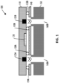
- FIG. 1 shows a cross section 100 of an integrated circuit (IC) 120 with antenna launchers 125A-B on the underside of a device package 110 affixed to a conventional PCB integrated waveguide 140 and an antenna array 150.
- the IC 120 can be a radar system, for example a millimeter (mm) wave radar system for automotive applications.
- the IC 120 is incorporated in the device package 110 with antenna launchers 125A-B positioned at the underside of the package 110.
- the device package 110 is attached to the waveguide 140 by grounded solder balls 130A and 130B, and the waveguide 140 is affixed to the antenna array 150.
- the antenna launchers 125A-B are aligned with the openings in the waveguide 140 and the antenna array 150 to form channels 160A-B.
- the antenna launchers 125A-B integrated in the underside of the device package 110 reduce the length of the feed lines to the antenna array 150
- the antenna launchers 125A-B increase the size and cost of the device package 110.
- the antenna launchers 125A-B must be aligned with openings in the waveguide 140 and the antenna array 150, increasing the manufacturing complexity.
- Some radar systems require reflection of the radiated signal, which increases the substrate thickness of the IC 120 and further increases the size and cost of device package 110.
- FIG. 2 shows a cross section of a system 200 affixed to an example printed circuit board (PCB) 250 with inductively coupled vertical signal launchers 230A-B, in accordance with an embodiment of the invention.
- PCB printed circuit board
- FIG. 2 is described herein with reference to the IC 120 and the grounded solder balls 130A-B in FIG. 1 .
- a package 210 includes the IC 120, semiconductor die-level signal interconnects 215A-B, and package-level signal interconnects 220A-B.
- the die-level signal interconnect 215A carries signals generated and received by the IC 120 between the IC 120 and the package-level signal interconnect 220A
- the die-level signal interconnect 215B carries signals generated and received by the IC 120 between the IC 120 and the package-level signal interconnect 220B.
- the package-level signal interconnects 220A-B can be signal output pins for the package 210, in some implementations.
- the package 210 is affixed to the PCB 250 by the grounded solder balls 130A and 130B.
- the PCB 250 has a number N of layers, including a first metal layer 250A, a second metal layer 250B, and third through the number N layers 250C-N.
- the layers 250A-N are substantially parallel to each other and substantially planar.
- channel regions 270A and 270B are substantially perpendicular to the layers 250A-N and extend from the second metal layer 250B to the Nth layer 250N.
- vertical means substantially perpendicular to a planar surface
- horizontal means substantially parallel to a planar surface.
- the channel regions 270A-B are filled with a different dielectric 285 than the dielectric 280 in the rest of the PCB 250.
- the channel regions 270A-B can be filled with the different dielectric 285 using a manufacturing process called plugging or can be left empty as air channels.
- the channel regions 270A-B have a same dielectric 285, but in other implementations, the channel region 270A has a different dielectric than the channel region 270B.
- the channel regions 270A-B are vertical waveguides as shown in FIG. 2 , but in other embodiments, the channel regions 270A-B are horizontal waveguides, such as substrate-integrated waveguides.
- the PCB 250 has a same dielectric 280 throughout the layers 250A-N, but in other implementations, as will be described further herein with respect to FIG. 3 , the PCB can include a different dielectric between layers 250B and 250N than the dielectric between layers 250A and 250B.
- signal solder balls 225A-B also affix the package 210 to the PCB 250.
- the signal solder ball 225A couples the package-level interconnect 220A to a via pad 275A in the first metal layer 250A of the PCB 250
- the signal solder ball 225B couples the package-level interconnect 220B to a via pad 275B included in the first metal layer 250B of the PCB 250.
- the vertical signal launchers 230A-B include conductive signal vias 235A-B, respectively, and pluralities of grounded vias 245A-B, respectively.
- the signal via 235A couples the via pad 275A in the first metal layer 250A to a connector 240A in the second metal layer 250B, inductively coupling the signal solder ball 225A to a channel 260A.
- the signal via 235B couples the via pad 275B in the first metal layer 250B to the connector 240B in the second metal layer 250B, inductively coupling the signal solder ball 225B to a channel 260B.
- the connectors 240A-B can be used to short the signal vias 235A-B to ground, such that a broken signal ball 225 or other discontinuity of the signal path can be detected by injecting a dc current.
- the signal vias 235A-B capacitively couple the signal solder balls 225A-B to the channels 260A-B, respectively, and are isolated within the vertical signal launchers 230A-B, as described further herein with reference to FIG. 3 .
- the second metal layer 250B is shown as the metal layer adjacent to the first metal layer 250A within the PCB 250, but in other implementations, one or more intervening layers, including intervening metal layers, can be present between the first metal layer 250A and the second metal layer 250B within the PCB 250.
- the pluralities of grounded vias 245A-B extend from the first layer 250A of the PCB 250 to the bottom, Nth layer 250N of the PCB 250 and have a height 265 between the first metal layer 250A and the second metal layer 250B plus a height 255 between the second metal layer 250B and the bottom, Nth layer 250N of the PCB 250.
- the plurality of grounded vias 245A form a boundary around the channel region 270A and signal via 235A and define the channel 260A. That is, the plurality of grounded vias 245A are arranged in a discontinuous ring bordering the channel region 270A and the signal via 235A, and form a cage to direct signal energy from the signal via 235A through the channel 260A.
- the plurality of grounded vias 245B form a boundary around the channel region 270B and the signal via 235B, and define the channel 260B. That is, the plurality of grounded vias 245B are arranged in a discontinuous ring bordering the channel region 270B and the signal via 235B, and form a cage to direct signal energy from the signal via 235B through the channel 260B.
- the pluralities of grounded vias 245A-B may be metallized and form a shield structure around the channel regions 270A-B and the signal vias 235A-B, respectively.
- the pluralities of grounded vias 245A-B form waveguides through the PCB 250 for signal energy radiated by the signal vias 235A-B. That is, the signal vias 235A-B and the connectors 240A-B inductively couple the signal solder balls 225A-B to the waveguides formed by the pluralities of grounded vias 245A-B.
- the package-level signal interconnect 220A is coupled to the signal via 235A in the PCB 250 by the signal solder ball 225A
- the package-level signal interconnect 220B is coupled to the signal via 235B in the PCB 250 by the signal solder ball 225B. Because the package-level signal interconnects 220A-B are coupled to the signal vias 235A-B by signal solder balls 225A-B, alignment between the package 210 and the PCB 250 is simplified compared to the alignment between the antenna launchers 125A-B in package 110 and the openings in waveguide 140 and the antenna array 150 shown in FIG. 1 , reducing the manufacturing complexity of the system 200.
- the package-level signal interconnects 220A-B are directly coupled to the signal vias 235A-B by the signal solder balls 225A-B, respectively, such that the package 210 can be affixed to the PCB 250 using standard ball grid array techniques.
- the package-level signal interconnects 220A-B bridge a vertical distance and a horizontal distance between the signal solder balls 225A-B and the die-level signal interconnects 215A-B
- the signal solder balls 225A-B are not horizontally offset from the die-level signal transitions 215A-B. That is, the signal solder balls 225A-B are underneath the die-level signal transitions 215A-B such that the package-level signal interconnects 220A-B bridge only a vertical distance between the signal solder balls 225A-B and the die-level signal interconnects 215A-B, as illustrated in FIG. 3 .
- the plurality of grounded solder balls 130A-B and the pluralities of grounded vias 245A-B form vertically-continuous metalized structures to shield the signal paths through the signal solder balls 225A-B, the signal vias 235A-B, and the channels 260A-B, respectively, reducing signal energy losses and cross talk between channels 260A and 260B.
- the pluralities of grounded vias 245A-B form waveguides for channels 260A-B, respectively, through the third layer 250C through Nth layer 250N of PCB 250.
- An external waveguide or antenna array 290 can be affixed to the opposite surface of the PCB 250 from the package 210.
- a substrate-integrated waveguide is incorporated in one or more layers of the third through Nth layers 250C-N of the PCB 250.
- the area of the PCB 250 occupied by the vertical signal launchers 230A-B is determined based on the height 265 between the first metal layer 250A and the second metal layer 250B in the PCB 250 and the dielectric material 285 of the channel regions 270A-B.
- the length of the inductive path along the signal via 235A and the portion of connector 240A grounding the signal via 235A to the grounded vias 245A is equal to approximately one-fourth of the signal wavelength in the dielectric 285.
- a system 200 has a dielectric-filled WR 12 waveguide, a height 265 equal to approximately 150 micrometers ( ⁇ m), and accommodates a 77 gigaHerz (GHz) signal.
- the length of the inductive path is approximately 150 ⁇ m plus 300 ⁇ m.
- the area of a surface of the PCB 250 occupied by a vertical signal launcher 230 is discussed further herein with respect to FIGS. 4-6 .
- FIG. 3 shows a cross section of a system 300 affixed to an example PCB 350 with capacitively coupled vertical signal launchers 330A-B, in accordance with an embodiment of the invention.
- FIG. 3 is described herein with reference to the IC 120 and the grounded solder balls 130A-B shown in FIG. 1 and the system 200 shown in FIG. 2 .
- the system 300 is similar to the system 200 shown in FIG. 2 , but includes capacitively coupled vertical signal launchers 330A-B, rather than inductively coupled vertical signal launchers 230A-B.
- a package 310 includes the IC 120, semiconductor die-level signal interconnects 315A-B, and package-level signal interconnects 320A-B.
- the die-level signal interconnect 315A carries signals generated and received by the IC 120 between the IC 120 and the package-level signal interconnect 320A
- the die-level signal interconnect 315B carries signals generated and received by the IC 120 between the IC 120 and the package-level signal interconnect 320B.
- the package 310 is affixed to a PCB 350 by the grounded solder balls 130A and 130B.
- the PCB 350 has a number N of layers, including a first metal layer 350A, a second metal layer 350B, and third through the number N layers 350C-N.
- the layers 350A-N are substantially parallel to each other and substantially planar.
- channel regions 370A and 370B are substantially perpendicular to the layers 350A-N and extend from the second metal layer 350B to the Nth layer 350N.
- the channel regions 370A-B are filled with a different dielectric 385 than the dielectric 380 in the rest of the PCB 350.
- the channel regions 370A-B can be filled with the different dielectric 385 using a manufacturing process called plugging or can be left empty as air channels.
- the channel regions 370A-B have a same dielectric 385, but in other implementations, the channel region 370A has a different dielectric than the channel region 370B.
- the channel regions 370A-B are vertical waveguides as shown in FIG. 3 , but in other embodiments, the channel regions 370A-B are horizontal waveguides, such as substrate-integrated waveguides.
- the PCB 350 has a first dielectric 380A between layers 350A and 350B and a second dielectric 380B between layers 350B and 350N.
- the PCB 350 can be pressed and cured during the manufacturing process, resulting in a first dielectric 380A between layers 350A and 350B and a second dielectric 380B between layers 350B and 350N.
- the PCB 350 can include the same dielectric 380 throughout the layers 350A-N, as described further herein with respect to FIG. 2 .
- signal solder balls 325A-B also affix the package 310 to the PCB 350.
- the signal solder ball 325A couples the package-level interconnect 320A to a via pad 375A in the first metal layer 350A of the PCB 350
- the signal solder ball 325B couples the package-level interconnect 320B to a via pad 375B in the first metal layer 350B of the PCB 350.
- the vertical signal launchers 330A-B include conductive signal vias 335A-B, respectively, and pluralities of grounded vias 345A-B, respectively.
- the signal via 335A couples the via pad 375A in the first metal layer 350A to a via pad 340A that is galvanically isolated within the channel region 370A from the second metal layer 350B and the plurality of grounded vias 345A, capacitively coupling the signal solder ball 325A to a channel 360A.
- the signal via 335B couples the via pad 375B in the first metal layer 350A to a via pad 340B that is galvanically isolated within the channel region 370B from the second metal layer 350B and the plurality of grounded vias 345B, capacitively coupling the signal solder ball 325B to a channel 360B.
- the second metal layer 350B is shown as the metal layer adjacent to the first metal layer 350A within the PCB 350, but in other implementations, one or more intervening layers, including intervening metal layers, can be present between the first metal layer 350A and the second metal layer 350B within the PCB 350.
- the pluralities of grounded vias 345A-B extend from the first layer 350A of the PCB 350 to the bottom, Nth layer 350N of the PCB 350 and have a height 365 between the first metal layer 350A and the second metal layer 350B plus a height 355 between the second metal layer 350B and the bottom, Nth layer 350N of the PCB 350.
- the plurality of grounded vias 345A form a boundary around the channel region 370A and the signal via 335A and define the channel 360A. That is, the plurality of grounded vias 345A are arranged in a discontinuous ring bordering the channel region 370A and the signal via 335A, and form a cage to direct signal energy from the signal via 335A through the channel 360A.
- the plurality of grounded vias 345B form a boundary around the channel region 370B and the signal via 335B and define the channel 360B. That is, the plurality of grounded vias 345B are arranged in a discontinuous ring bordering the channel region 370B and the signal via 335B, and form a cage to direct signal energy from the signal via 335B through the channel 360B.
- the grounded vias 345A-B may be metallized and form a shield structure around the signal vias 335A-B.
- the pluralities of grounded vias 345A-B form waveguides through the PCB 350 for signal energy radiated by the signal vias 335A-B. That is, the signal vias 335A-B capacitively couple the signal solder balls 325A-B to the waveguides formed by the pluralities of grounded vias 345A-B.
- the package-level signal interconnect 320A is coupled to the signal via 335A in the PCB 350 by the signal solder ball 325A
- the package-level signal interconnect 320B is coupled to the signal via 335B in the PCB 350 by the signal solder ball 325B. Because the package-level signal interconnects 320A-B are coupled to the signal vias 335A-B by signal solder balls 325A-B, alignment between the package 310 and the PCB 350 is simplified compared to the alignment between the antenna launchers 125A-B in package 110 and the openings in waveguide 140 and the antenna array 150 shown in FIG. 1 , reducing the manufacturing complexity of the system 300.
- the package-level signal interconnects 320A-B are directly coupled to the signal vias 335A-B by the signal solder balls 325A-B, respectively, such that the package 310 can be affixed to the PCB 350 using standard ball grid array techniques.
- the package-level signal interconnects 320A-B bridge only a vertical distance between the signal solder balls 325A-B and the die-level signal interconnects 315A-B
- the signal solder balls 325A-B are horizontally offset from the die-level signal interconnects 315A-B. That is, the signal solder balls 325A-B are not directly underneath the die-level signal interconnects 315A-B such that the package-level signal interconnects 320A-B bridge both a vertical distance and a horizontal distance between the signal solder balls 325A-B and the die-level signal interconnects 315A-B, as illustrated in FIG. 2 .
- the package-level signal interconnects 320A-B can be signal output pins for the package 310, in some implementations.
- the plurality of grounded solder balls 130A-B and the pluralities of grounded vias 345A-B form vertically-continuous metalized structures to shield the signal paths through the signal solder balls 325A-B, the signal vias 335A-B, and the channels 360A-B, respectively, reducing signal energy losses and cross talk between channels 360A and 360B.
- the pluralities of grounded vias 345A-B form waveguides for channels 360A-B, respectively, through the third layer 350C through Nth layer 350N of PCB 350.
- An external waveguide or antenna array 390 can be affixed to the opposite surface of the PCB 350 from the package 310.
- a substrate-integrated waveguide is incorporated in one or more layers of the third through Nth layers 350C-N of the PCB 350.
- the area of the PCB 350 occupied by the vertical signal launchers 330A-B is determined based on the height 365 between the first metal layer 350A and the second metal layer 350B in the PCB 350 and the dielectric material 385 of the channel regions 370A-B.
- a standard PCB layer height 365 can be used, such as 127 ⁇ m.
- An external waveguide or antenna array 390 can be coupled to the opposite side of the PCB 350 from the package 310.
- a substrate-integrated waveguide is incorporated in one or more layers of the third through Nth layers 350C-N of the PCB 350.
- FIG. 4 shows an overhead view of a first metal layer 400 of an example PCB vertical signal launcher, such as the inductively coupled vertical signal launchers 230A-B shown in FIG. 2 and the capacitively coupled vertical signal launchers 330A-B shown in FIG. 3 , in accordance with an embodiment of the invention. That is, the overhead view of the first metal layer 400 shown in FIG. 4 corresponds to a portion of the first metal layer 250A shown in FIG. 2 that includes the vertical signal launcher 230A and to a portion of the first metal layer 350A shown in FIG. 3 that includes the vertical signal launcher 330A.
- the example PCB vertical signal launcher is rectangular in shape and has a width W 405 and a height H 410.
- the height H 410 is approximately twice the width W 405.
- the width W 405 is approximately 600 ⁇ m
- the height H 410 is approximately 1200 ⁇ m.
- the first metal layer 400 includes portions of metallized, grounded vias 445 which form a boundary around the opening 430, which is an opening of a PCB channel region such as channel region 270 shown in FIG. 2 and channel region 370 shown in FIG. 3 . That is, the plurality of grounded vias 445 are arranged in a discontinuous ring around the opening 430 of the channel region and form a cage to direct signal energy.
- a distance P 440 between the grounded vias 445 can be any appropriate distance such that the vias 445 direct signal energy through the PCB.
- the distance P 440 can be a standard manufacturing distance such as 0.5 mm or 0.65 mm in some implementations.
- a signal via 435 is coupled to a via pad 425 on which a signal solder ball is configured to be coupled.
- the term "via pad” and “solder pad” are used interchangeably herein.
- the signal solder ball 225A is coupled to the via pad 275A
- the signal solder ball 325A is coupled to the via pad 375A.
- the opening 430 in the metal layer 400 has a diameter D_ground 455, and the signal via 435 has a diameter D_via 450 within the opening 430. That is, the channel region corresponding to opening 430 has a diameter D_ground 455, and within the channel region corresponding to opening 430, the signal via 435 has a diameter D_via 450.
- FIG. 5 shows overhead views of a second metal layer 500 of an example inductively coupled PCB vertical signal launcher, such as the inductively coupled PCB vertical signal launchers 230A-B shown in FIG. 2 , and a second metal layer 550 of an example capacitively coupled PCB vertical signal launcher, such as the capacitively coupled PCB vertical signal launchers 330A-B shown in FIG. 3 , in accordance with embodiments of the invention. That is, the overhead view of the second metal layer 500 shown in FIG. 5 corresponds to a portion of the second metal layer 250B shown in FIG. 2 that includes the vertical signal launcher 230A, and the overhead view of the second metal layer 550 shown in FIG. 5 corresponds to a portion of the second metal layer 350B shown in FIG. 3 that includes the vertical signal launcher 330A.
- the second metal layers 500 and 550 are described herein with reference to the first metal layer 400 shown in FIG. 4 .
- the second metal layers 500 and 550 include portions of the plurality of metallized, grounded vias 445 around a cross section 520 of the channel region, which includes a non-metalized dielectric PCB material such as dielectric 285 shown in FIG. 2 or dielectric 385 shown in FIG. 3 .
- the cross section 520 is a waveguide opening within the second metal layers 500 and 550 and has a rectangular shape in this example, with a width W_inner 505 and a height H_inner 510. In some implementations, the height H_inner 510 is approximately twice the width W_inner 505.
- the signal via 435 is coupled to a via pad 530 in the second metal layers 500 and 550.
- the via pad 530 is inductively coupled to the surrounding metal by a connector 540.
- the signal via 235A is coupled to the surrounding metal layer 250B by the connector 240B.
- the via pad 530 is galvanically isolated or floating within the cross section 520 of the channel region.
- the signal via 335A is coupled to the via pad 340A that is isolated within the channel region 370A of the second metal layer 350B.
- FIG. 6 shows an overhead view of an additional layer 600 of the example PCB with vertical signal launchers, such as the inductively coupled vertical signal launchers 230A-B shown in FIG. 2 and the capacitively coupled vertical signal launchers 330A-B shown in FIG. 3 , in accordance with an embodiment of the invention.
- the PCB includes a number N of layers.
- the additional layer 600 illustrates the shape of the example vertical signal launcher in the third layer through the Nth layer of the PCB. That is, the overhead view of the additional layer 600 shown in FIG. 6 corresponds to a portion of a layer among the layers 250C-N shown in FIG. 2 that includes the vertical signal launcher 230A and to a portion of a layer among the layers 350C-N shown in FIG. 3 that includes the vertical signal launcher 330A.
- the additional layer 600 is described herein with reference to the first metal layer 400 shown in FIG. 4 and the second metal layers 500 and 550 shown in FIG. 5 .
- the additional layer 600 includes a portion of the plurality of metallized, grounded vias 445 around a cross section 620 of the channel region, which includes a non-metalized dielectric PCB material such as dielectric 285 shown in FIG. 2 or dielectric 385 shown in FIG. 3 .
- the cross section 620 is the same rectangular shape as the cross section 520 in second metal layers 500 and 550 shown in FIG. 5 , and has the width W_inner 505 and height H_inner 510.
- the cross section 620 can be a different shape than the cross section 520 in the second metal layers 500 and 550.
- FIG. 7 shows cross sections 700 and 750 of an example PCB with an inductively coupled vertical signal launcher such as the vertical signal launcher 230A shown in FIG. 2 being formed by mechanical drilling, in accordance with an embodiment of the invention.
- cross sections 700 and 750 are described herein with reference to metal layers 400 and 500 shown in FIGS. 4 and 5 , respectively.
- the cross section 700 shows the example PCB at a first stage of the manufacturing process, in which a mechanical drill is used to drill a first portion 735A of the signal via.
- the mechanical drill can form a so-called "blind" via between the first via pad 425 in the first metal layer 400 and the second via pad 530 in the second metal layer 500 within a channel region 770.
- a dielectric thickness 765 between the first metal layer 400 and the second metal layer 500 is approximately 150 ⁇ m, and the first portion 735A of the signal via can be drilled in a single step.
- the channel region 770 can be filled with a dielectric 785 that is different from a dielectric in the rest of the PCB.
- the example PCB also includes the plurality of grounded vias 445, which form a border around the signal via 735.
- the signal via 735 is inductively coupled to the plurality of grounded vias 445 by the connector 540 in the second metal layer 500.
- the area of the PCB bordered by the grounded vias 445 and the channel region 770 in which the signal via 735B is drilled forms a channel 760.
- the plurality of grounded vias 445 can be formed by first mechanically drilling from the first metal layer 400 to the Nth layer 710N of the PCB, creating PCB through-holes.
- the PCB through-holes may then be metal plated to finish construction of the grounded vias 445.
- the first portion 735A of the signal via is metal plated in a second stage of the manufacturing process, as illustrated in cross section 750 of the example PCB.
- the drilled portion 735A of the signal via can be metal plated and filled with copper to form the completed signal via 735B.
- construction of the metal plated signal via 735B is completed.
- the plating layer of the completed signal via 735B has a different coefficient of thermal expansion and material stiffness than the metal filling the plated portion of the signal via 735B.
- the differences in thermal expansion and stiffness between the two materials can impact stress and strain inside the signal solder balls 225A-B for inductively coupled vertical signal launchers or signal solder balls 325A-B for capacitively coupled vertical signal launchers during temperature cycling of turn-on and turn-off of the signal generator and receiver in the IC 120.
- underfill materials may be applied between the package 210 or 310 and the PCBs 250 or 350, respectively. Because the signal solder balls 225A-B and 325A-B are shielded by grounded solder balls 130A-B, the underfill material has a reduced impact on transmission energy loss.
- FIG. 8 shows a cross section 800 of an example PCB with an inductively coupled vertical signal launcher such as the vertical signal launcher 230A shown in FIG. 2 formed by a combination of laser drilling and mechanical drilling, in accordance with an embodiment of the invention.
- cross section 800 is described herein with reference to metal layers 400 and 500 shown in FIGS. 4 and 5 , respectively.
- the cross section 800 shows a signal via 835 formed by laser drilling.
- a laser-drilled via is also referred to herein as a microvia. Laser drilling enables a smaller via diameter than mechanical drilling, and so vertical signal launchers including laser-drilled vias can be smaller than vertical signal launchers including mechanically-drilled vias.
- the signal via 835 is formed by laser drilling, and the plurality of grounded vias 445 are formed by mechanical drilling. In other implementations, both the signal via 835 and the plurality of grounded vias 445 are formed by laser drilling.
- the microvia 835 extends a height 865 from the first via pad 425 in the first metal layer 400 to the second via pad 530 in the second metal layer 500 within a channel region 870.
- the channel region 870 can be filled with a dielectric 885 that is different from a dielectric in the rest of the PCB.
- the plurality of grounded vias 445 extend from the first metal layer 400 to the bottom, Nth layer 810N of the PCB.
- the signal via 835 is inductively coupled to the plurality of grounded vias 445 by the connector 540 in the second metal layer 500.
- the area of the PCB bordered by the grounded vias 445 and the channel region 870 in which the signal via 835 is drilled forms a channel 860.
- FIG. 9 shows a cross section 900 of an example PCB with an inductively coupled vertical signal launcher such as the vertical signal launcher 230A shown in FIG. 2 formed by a combination of laser drilling and mechanical drilling, in accordance with an embodiment of the invention.
- cross section 900 is described herein with reference to metal layers 400 and 500 shown in FIGS. 4 and 5 , respectively.
- the cross section 900 includes a signal via 935 that is formed by laser drilling, and the plurality of grounded vias 445 that are formed by mechanical drilling. In other implementations, both the signal via 935 and the plurality of grounded vias 445 are formed by laser drilling.
- the signal via 935 includes stacked microvias that extend a height 965 from the first via pad 425 in the first metal layer 400 to the second via pad 530 in the second metal layer 500 within a channel region 970.
- the height 965 is 150 ⁇ m
- each microvia in the stack is approximately 75 ⁇ m.
- the channel region 970 can be filled with a dielectric 985 that is different from a dielectric in the rest of the PCB.
- the plurality of grounded vias 445 extend from the first metal layer 400 to the bottom, Nth layer 910N of the PCB.
- the signal via 935 is inductively coupled to the plurality of grounded vias 445 by the connector 540 in the second metal layer 500.
- the area of the PCB bordered by the plurality of grounded vias 445 and the channel region 970 in which the signal via 935 is drilled forms a channel 960.
- FIG. 10 shows a cross section 1000 of an example PCB with an inductively coupled vertical signal launcher such as the vertical signal launcher 230A shown in FIG. 2 , including a signal microvia 1035 formed by laser drilling and a plurality of grounded vias 1045 formed by a combination of mechanical drilling and laser drilling, in accordance with an embodiment of the invention.
- cross section 1000 is described herein with reference to metal layers 400 and 500 shown in FIGS. 4 and 5 , respectively.
- the cross section 1000 shows a signal via 1035 having a single microvia within a channel region 1070 and the plurality of grounded vias 1045 around the channel region 1070.
- the signal via 1035 extends a height 1065 from the first via pad 425 in the first metal layer 400 to the second via pad 530 in the second metal layer 500 within the channel region 1070.
- the channel region 1070 can be filled with a dielectric 1085 that is different from a dielectric in the rest of the PCB.
- Each grounded via 1045 has a mechanically drilled portion 1045A and two laser-drilled portions 1045B-C.
- the first laser-drilled portion 1045B extends from the first metal layer 400 to the second metal layer 500 and has a height 1065.
- the second laser-drilled portion 1045C extends inward from the bottom Nth layer 1010N.
- the first and second laser-drilled portions 1045B-C are bridged by the mechanically drilled portion 1045A.
- the area of the PCB bordered by the grounded vias 1045 and the channel region 1070 in which the signal via 1035 is drilled forms a channel 1060.
- FIG. 11 shows a cross section 1100 of an example PCB with an inductively coupled vertical signal launcher such as the vertical signal launcher 230A shown in FIG. 2 , including a signal microvia 1135 formed by laser drilling and a plurality of grounded vias 1145 formed by a combination of mechanical drilling and laser drilling, in accordance with an embodiment of the invention.
- a signal microvia 1135 formed by laser drilling and a plurality of grounded vias 1145 formed by a combination of mechanical drilling and laser drilling, in accordance with an embodiment of the invention.
- cross section 1100 is described herein with reference to metal layers 400 and 500 shown in FIGS. 4 and 5 , respectively.
- the signal via 1135 includes stacked microvias within a channel region 1170, which can be filled with a dielectric 1185 that is different from a dielectric in the rest of the PCB.
- Each grounded via 1145 includes a mechanically drilled portion 1145A and two laser-drilled, stacked microvia portions 1145B-C.
- the first stacked microvia portion 1145B extends from the first metal layer 400 to the second metal layer 500 and has a height 1165.
- the second stacked microvia portion 1145C extends inward from the bottom Nth layer 1110N.
- the first and second laser-drilled portions 1145B-C are bridged by the mechanically drilled portion 1145A.
- the area of the PCB bordered by the grounded vias 1145 and the channel region 1170 in which the signal via 1135 is drilled forms a channel 1160.
- FIG. 12 shows a cross section 1200 of an example PCB with an inductively coupled vertical signal launcher such as the vertical signal launcher 230A shown in FIG. 2 , including a signal microvia 1235 and a plurality of grounded vias 1245 formed by laser drilling, in accordance with an embodiment of the invention.
- cross section 1200 is described herein with reference to metal layers 400 and 500 shown in FIGS. 4 and 5 , respectively.
- the signal via 1235 includes a single microvia within a channel region 1270, which can be filled with a dielectric 1285 that is different from a dielectric in the rest of the PCB.
- Each grounded via 1245 includes an x-shaped via 1245A and microvia portions 1245B-C.
- the first microvia portion 1245B extends from the first metal layer 400 to the second metal layer 500 and has a height 1265.
- the second microvia portion 1245C extends inward from the bottom Nth layer 1210N.
- the first and second microvia portions 1245B-C are bridged by the x-shaped via portion 1245A, which is formed by sequential top and bottom side laser drilling.
- the area of the PCB bordered by the grounded vias 1245 and the channel region 1270 in which the signal via 1235 is drilled forms a channel 1260.
- FIG. 13 shows a cross section 1300 of an example PCB with an inductively coupled vertical signal launcher such as the vertical signal launcher 230A shown in FIG. 2 , including a stacked signal microvia 1335 and a plurality of grounded vias 1345 formed by laser drilling, in accordance with an embodiment of the invention.
- cross section 1300 is described herein with reference to metal layers 400 and 500 shown in FIGS. 4 and 5 , respectively.
- the signal via 1335 includes stacked microvias within a channel region 1370, which can be filled with a dielectric 1385 that is different from a dielectric in the rest of the PCB.
- Each grounded via 1345 includes an x-shaped via 1345A and stacked microvia portions 1345B-C.
- the first stacked microvia portion 1345B extends from the first metal layer 400 to the second metal layer 500 and has a height 1365.
- the second stacked microvia portion 1345C extends inward from the bottom Nth layer 1310N.
- the first and second stacked microvia portions 1345B-C are bridged by the x-shaped via portion 1345A.
- the area of the PCB bordered by the grounded vias 1345 and the channel region 1370 in which the signal via 1335 is drilled forms a channel 1360.
- the example PCBs shown in FIGS. 8-13 include inductively coupled vertical signal launchers such as the vertical signal launcher 230A shown in FIG. 2 , but in other implementations the example PCBs include capacitively coupled vertical signal launchers such as the vertical signal launcher 330A shown in FIG. 3 .
- the combinations of single and stacked microvias formed by laser drilling and mechanically drilled vias shown in FIGS. 8-13 are for illustration only, and in other implementations, other combinations can be used.
- FIGS. 1-13 illustrate single ended vertical signal launchers, but in other implementations, the example PCB vertical signal launchers may be differential, as illustrated in FIGS. 14-16 .
- FIG. 14 shows an overhead view of a first metal layer 1400 of an example PCB vertical differential signal launcher, similar to the inductively coupled vertical signal launchers 230A-B shown in FIG. 2 and the capacitively coupled vertical signal launchers 330A-B shown in FIG. 3 , in accordance with an embodiment of the invention.
- the example PCB vertical signal launcher is rectangular in shape and has a width W 1405 and a height H 1410. In some implementations, the height H 1410 is approximately twice the width W 1405.
- the first metal layer 1400 includes portions of metallized, grounded vias 1445 which form a boundary around an opening 1430, which is an opening of a PCB channel region in some embodiments from the top surface of the PCB to the bottom surface of the PCB. That is, the plurality of grounded vias 1445 are arranged in a discontinuous ring around the opening 1430 of the channel region and form a cage to direct signal energy.
- a distance P 1440 between the grounded vias 1445 can be any appropriate distance such that the vias 1445 direct the signal energy through the PCB.
- the distance P 1440 can be a standard manufacturing distance such as 0.5 mm or 0.65 mm in some implementations.
- differential signal vias 1435A-B are coupled to solder pads 1425A-B, respectively, on which signal solder balls are configured to be coupled.
- the signal solder ball 225A can be coupled to the via pad 1425A or 1425B
- the signal solder ball 325A can be coupled to the via pad 1425A or 1425B.
- the opening 1430 in the grounded metal layer 1400 has a diameter D_ground 1455, and within the channel region corresponding to opening 1430, the signal vias 1435A and 1435B each have a diameter D_via 1450.
- FIG. 15 shows an overhead view of a second metal layer 1500 of an example inductively coupled, differential PCB vertical signal launcher, such as the inductively coupled PCB vertical signal launchers 230A-B shown in FIG. 2 , in accordance with an embodiment of the invention.
- the second metal layer 1500 is described herein with reference to the first metal layer 1400 shown in FIG. 14 .
- the second metal layer 1500 includes the plurality of metallized, grounded vias 1445 around a cross section 1520 of the channel region, which includes a non-metalized dielectric PCB material such as dielectric 285 shown in FIG. 2 .
- the cross section 1520 can be a waveguide opening within the second metal layer 1500 and has a rectangular shape in this example, with a width W_inner 1505 and a height H_inner 1510. In some implementations, the height H_inner 1510 is approximately twice the width W inner 1505.
- the metal enclosing the cross section 1520 of the channel region can have a manufacturing width needed to enclose the plurality of grounded vias 1445 or can be part of a ground plane layer.
- the signal vias 1435A-B are coupled to via pads 1530A-B, respectively, in the second metal layer 1500.
- the via pads 1530A-B are galvanically coupled to the surrounding metal by the connectors 1540.
- a broken signal ball or other discontinuity of the signal path can be detected by injecting a dc current.
- a second metal layer 1500 for a capacitively coupled differential signal launcher omits the connectors 1540, and the via pads 1530A-B are galvanically isolated within the cross section 1520.
- FIG. 16 shows an overhead view of an additional layer 1600 of the example PCB with differential vertical signal launchers, such as the inductively coupled vertical signal launchers 230A-B shown in FIG. 2 and the capacitively coupled vertical signal launchers 330A-B shown in FIG. 3 , in accordance with an embodiment of the invention.
- the PCB includes a number N layers.
- the additional layer 1600 illustrates the shape of the example vertical signal launcher in the third layer through the Nth layer of the PCB.
- the additional layer 1600 is described herein with reference to the first metal layer 1400 shown in FIG. 14 and the second metal layer 1500 shown in FIG. 15 .
- the additional layer 1600 includes a portion of the plurality of metallized, grounded vias 1445 around a cross section 1620 of the channel region, which includes a non-metalized dielectric PCB material such as dielectric 285 shown in FIG. 2 or the dielectric 385 shown in FIG. 3 .
- the cross section 1620 is the same rectangular shape as the cross section 1520 in the second metal layer 1500 shown in FIG. 15 , and has the width W_inner 1505 and height H_inner 1510. In other implementations, the cross section 1620 has a different shape than the cross section 1520 in the second metal layer 1500.
- the disclosed vertical signal launchers simplify alignment of the device package and the PCB by directly coupling signal interconnects in the package to the signal vias in the PCB with signal solder balls.
- the direct connection reduces the number of signal transitions and the corresponding loss of signal strength.
- the plurality of grounded vias around a signal via and the plurality of grounded solder balls around a signal solder ball in one embodiment of the disclosed vertical signal launchers form a cage to direct signal energy through the PCB to a substrate-integrated or external waveguide or external antenna or the like, while reducing interference and cross-talk between adjacent channels.
- the disclosed vertical signal launchers can be manufactured using standard techniques and materials.
- Couple may cover connections, communications, or signal paths that enable a functional relationship consistent with this description, including intermediate or intervening components that do not alter the functional relationship.
- a device that is "configured to" perform a task or function may be configured by programming or hardwiring, for example, at a time of manufacturing by a manufacturer and/or may be configurable or reconfigurable by a user after manufacturing. The configuring may be done through firmware and/or software, construction and/or layout of hardware components and connections, or any combination thereof.
- node "pin”, and “lead” are used interchangeably.
- a circuit or device described herein as including certain components may be adapted to be coupled to those components instead, to form the described circuitry or device.
- An apparatus includes a PCB, a solder pad, a signal via, a plurality of metalized vias, and a waveguide.
- the PCB has a first surface opposite a second surface and includes a first metal layer, a second metal layer having a waveguide opening, and a PCB channel region from the waveguide opening in the second metal layer to the second surface of the PCB.
- the solder pad is positioned on the first surface of the PCB over the PCB channel region, and the signal via is coupled to the solder pad and to a via pad in the second metal layer within the waveguide opening.
- the plurality of metalized vias extend from the first surface to the second surface of the PCB and form a boundary around the PCB channel region.
- the waveguide is affixed to the waveguide opening in the second metal layer.
- the waveguide is a substrate-integrated waveguide incorporated in the PCB.
- the waveguide can include the plurality of metalized vias from the second metal layer to the second surface of the PCB.
- the apparatus further includes a device affixed to the first surface of the PCB.
- the device includes an integrated circuit and a signal output pin coupled to the integrated circuit.
- a signal solder ball couples the signal output pin to the solder pad on the first surface of the PCB.
- a plurality of grounded solder balls affix the device to the plurality of metalized vias.
- the signal via inductively couples the signal solder ball to the waveguide.
- a PCB having a first surface opposite a second surface includes a vertical signal launcher.
- the vertical signal launcher includes a PCB channel region, a signal via, and a plurality of metalized vias.
- the signal via is coupled to a first via pad in a first metal layer of the PCB and to a second via pad in a second metal layer of the PCB.
- the PCB channel region extends from the second metal layer of the PCB to the second surface of the PCB.
- the plurality of metalized vias extend from the first surface of the PCB to the second surface of the PCB and form a boundary around the PCB channel region.
- a device package is affixed to the first surface of the PCB, and the device package includes an integrated circuit and a signal output pin coupled to the integrated circuit.
- a signal solder ball couples the signal output pin to the first via pad in the vertical signal launcher of the PCB.
- a plurality of grounded solder balls affix the device package to the plurality of metalized vias.
- the signal via capacitively couples the signal solder ball to a waveguide in the vertical signal launcher, and the waveguide includes the plurality of metalized vias from the second metal layer to the second surface of the PCB. The signal via is substantially isolated within the plurality of metalized vias.
- the signal via inductively couples the signal solder ball to a waveguide in the vertical signal launcher, and the waveguide includes the plurality of metalized vias from the second metal layer to the second surface of the PCB.
- the signal via is galvanically coupled to the second metal layer.
- an external waveguide is affixed to the second surface of the PCB.
- the PCB may further include a substrate-integrated waveguide adjacent to the second metal layer of the PCB.
- a method includes forming a signal via and a solder pad in a PCB.
- the signal via extends from a first metal layer of the PCB to a second metal layer of the PCB, and the solder pad is positioned on a first surface of the PCB and coupled to the signal via.
- a channel region is formed from the second metal layer of the PCB to a second surface of the PCB opposite the first surface of the PCB.
- a plurality of grounded vias are formed from the first metal layer to the second surface of the PCB, such that the plurality of grounded vias border the channel region.
- the signal via and/or the plurality of grounded vias are mechanically drilled through the PCB.
- the signal via and/or the plurality of grounded vias are laser drilled through the PCB.
- each grounded via in the plurality of grounded vias are formed by laser drilling a first microvia from the first surface of the PCB, laser drilling a second microvia from the second surface of the PCB, and mechanically drilling between the first microvia and the second microvia.
Abstract
An apparatus includes a printed circuit board (PCB), a solder pad, a signal via, a plurality of metalized vias, and a waveguide. The PCB has a first surface opposite a second surface and includes a first metal layer, a second metal layer having a waveguide opening, and a PCB channel region from the waveguide opening in the second metal layer to the second surface. The solder pad is positioned on the first surface of the PCB over the channel region, and the signal via is coupled to the solder pad and a via pad in the second metal layer within the waveguide opening. The plurality of metalized vias extend from the first surface to the second surface of the PCB and form a boundary around the channel region. The waveguide is affixed to the waveguide opening in the second metal layer.
Description
- Losses from signal transmission feedlines between antenna launchers within a transceiver circuit and external antenna arrays or waveguides have prompted the integration of antenna launchers into packaging and the development of three-dimensional (3D) waveguide antennas. However, integration of the antenna launcher increases the size of the package envelope and the corresponding manufacturing cost. In addition, the alignment of the antenna launchers with the 3D waveguide can increase the manufacturing complexity.
- The present invention may be better understood, and its numerous objects, features, and advantages made apparent to those skilled in the art by referencing the accompanying drawings.
-
FIG. 1 shows a cross section of an integrated circuit (IC) with antenna launchers on the underside of the device package affixed to a conventional waveguide and antenna array. -
FIG. 2 shows a cross section of a system affixed to an example printed circuit board (PCB) with inductively coupled vertical signal launchers, in accordance with one embodiment of the present invention. -
FIG. 3 shows a cross section of a system affixed to an example PCB with capacitively coupled vertical signal launchers, in accordance with an embodiment of the present invention. -
FIG. 4 shows an overhead view of a first metal layer of an example PCB vertical signal launcher, such as the inductively coupled vertical signal launchers shown inFIG. 2 and the capacitively coupled vertical signal launchers shown inFIG. 3 , in accordance with an embodiment of the present invention. -
FIG. 5 shows overhead views of a second metal layer of an example inductively coupled PCB vertical signal launcher, such as the inductively coupled PCB vertical signal launcher shown inFIG. 2 ., and a second metal layer of an example capacitively coupled PCB vertical signal launcher, such as the capacitively coupled PCB vertical signal launcher shown inFIG. 3 , in accordance with an embodiment of the present invention. -
FIG. 6 shows an overhead view of an additional layer of the example PCB with vertical signal launchers, such as the inductively coupled vertical signal launchers shown inFIG. 2 and the capacitively coupled vertical signal launchers shown inFIG. 3 , in accordance with an embodiment of the present invention. -
FIG. 7 shows cross sections of an example PCB with an inductively coupled vertical signal launcher being formed by mechanical drilling, in accordance with an embodiment of the present invention. -
FIG. 8 shows a cross section of an example PCB with an inductively coupled vertical signal launcher formed by a combination of laser drilling and mechanical drilling, in accordance with an embodiment of the present invention. -
FIG. 9 shows a cross section of an example PCB with an inductively coupled vertical signal launcher formed by a combination of laser drilling and mechanical drilling, in accordance with an embodiment of the present invention. -
FIG. 10 shows a cross section of an example PCB with an inductively coupled vertical signal launcher including a signal microvia formed by laser drilling and a plurality of grounded vias formed by a combination of mechanical drilling and laser drilling, in accordance with an embodiment of the present invention. -
FIG. 11 shows a cross section of an example PCB with an inductively coupled vertical signal launcher including a signal microvia formed by laser drilling and a plurality of grounded vias formed by a combination of mechanical drilling and laser drilling, in accordance with an embodiment of the present invention. -
FIG. 12 shows a cross section of an example PCB with an inductively coupled vertical signal launcher including a signal microvia and a plurality of grounded vias formed by laser drilling, in accordance with an embodiment of the present invention. -
FIG 13 shows a cross section of an example PCB with an inductively coupled vertical signal launcher including a stacked signal microvia and a plurality of grounded vias formed by laser drilling, in accordance with an embodiment of the present invention. -
FIG. 14 shows an overhead view of a first metal layer of an example differential PCB vertical signal launcher, such as the inductively coupled vertical signal launchers shown inFIG. 2 and the capacitively coupled vertical signal launchers shown inFIG. 3 , in accordance with an embodiment of the present invention. -
FIG. 15 shows overhead views of a second metal layer of an example inductively coupled, differential PCB vertical signal launcher, such as the inductively coupled PCB vertical signal launcher shown inFIG. 2 , in accordance with an embodiment of the present invention. -
FIG. 16 shows an overhead view of an additional layer of the example PCB with differential vertical signal launchers, such as the inductively coupled vertical signal launchers shown inFIG. 2 and the capacitively coupled vertical signal launchers shown inFIG. 3 , in accordance with an embodiment of the present invention. - The use of the same reference symbols in different drawings indicates identical items unless otherwise noted. The Figures are not necessarily drawn to scale.
- In conventional systems, the integration of the antenna launcher into the packaging increases the size of the package envelope, and alignment of the integrated antenna launchers with the 3D waveguide can increase the manufacturing complexity of the system as a whole. To address these challenges, embodiments of the disclosed invention combine the function of affixing a device package to a printed circuit board (PCB) with launching signals from the device package. In embodiments of the disclosed invention, signal solder balls help affix device packages to PCBs and carry signals between package-level signal interconnects and signals vias in the PCBs. Within the PCBs, signal vias radiate signals between the signal solder balls and waveguides and vice versa. The waveguides can be external 3D waveguides or substrate-integrated waveguides, and pluralities of grounded vias form borders around the signal vias.
- Pluralities of grounded solder balls form borders around the signal solder balls and help affix the device packages to the PCBs more securely. The pluralities of grounded solder balls and grounded vias also help isolate the signal solder balls and signal vias, respectively, to reduce signal interference, channel cross-talk, and the like. The direct connection provided by the signal solder balls between package-level signal interconnects in the device packages and the signal vias in the PCBs simplify alignment between the device packages and the PCBs relative to conventional systems, such as the example shown in
FIG. 1 . -
FIG. 1 shows across section 100 of an integrated circuit (IC) 120 withantenna launchers 125A-B on the underside of adevice package 110 affixed to a conventional PCB integratedwaveguide 140 and anantenna array 150. The IC 120 can be a radar system, for example a millimeter (mm) wave radar system for automotive applications. The IC 120 is incorporated in thedevice package 110 withantenna launchers 125A-B positioned at the underside of thepackage 110. Thedevice package 110 is attached to thewaveguide 140 bygrounded solder balls waveguide 140 is affixed to theantenna array 150. Theantenna launchers 125A-B are aligned with the openings in thewaveguide 140 and theantenna array 150 to formchannels 160A-B. - While the
antenna launchers 125A-B integrated in the underside of thedevice package 110 reduce the length of the feed lines to theantenna array 150, theantenna launchers 125A-B increase the size and cost of thedevice package 110. In addition, theantenna launchers 125A-B must be aligned with openings in thewaveguide 140 and theantenna array 150, increasing the manufacturing complexity. Some radar systems require reflection of the radiated signal, which increases the substrate thickness of theIC 120 and further increases the size and cost ofdevice package 110. -
FIG. 2 shows a cross section of asystem 200 affixed to an example printed circuit board (PCB) 250 with inductively coupledvertical signal launchers 230A-B, in accordance with an embodiment of the invention. For ease of explanation,FIG. 2 is described herein with reference to theIC 120 and the groundedsolder balls 130A-B inFIG. 1 . Apackage 210 includes the IC 120, semiconductor die-level signal interconnects 215A-B, and package-level signal interconnects 220A-B. The die-level signal interconnect 215A carries signals generated and received by theIC 120 between theIC 120 and the package-level signal interconnect 220A, and the die-level signal interconnect 215B carries signals generated and received by theIC 120 between theIC 120 and the package-level signal interconnect 220B. The package-level signal interconnects 220A-B can be signal output pins for thepackage 210, in some implementations. - The
package 210 is affixed to the PCB 250 by the groundedsolder balls first metal layer 250A, asecond metal layer 250B, and third through thenumber N layers 250C-N. Thelayers 250A-N are substantially parallel to each other and substantially planar. Within thePCB 250,channel regions layers 250A-N and extend from thesecond metal layer 250B to the Nth layer 250N. As used herein, "vertical" means substantially perpendicular to a planar surface, while "horizontal" means substantially parallel to a planar surface. - In some embodiments, the
channel regions 270A-B are filled with a different dielectric 285 than the dielectric 280 in the rest of thePCB 250. For example, thechannel regions 270A-B can be filled with the different dielectric 285 using a manufacturing process called plugging or can be left empty as air channels. In this example, thechannel regions 270A-B have a same dielectric 285, but in other implementations, thechannel region 270A has a different dielectric than thechannel region 270B. In some embodiments, thechannel regions 270A-B are vertical waveguides as shown inFIG. 2 , but in other embodiments, thechannel regions 270A-B are horizontal waveguides, such as substrate-integrated waveguides. - In this example implementation, the PCB 250 has a same dielectric 280 throughout the
layers 250A-N, but in other implementations, as will be described further herein with respect toFIG. 3 , the PCB can include a different dielectric betweenlayers 250B and 250N than the dielectric betweenlayers solder balls 130A-B,signal solder balls 225A-B also affix thepackage 210 to the PCB 250. Thesignal solder ball 225A couples the package-level interconnect 220A to avia pad 275A in thefirst metal layer 250A of the PCB 250, and thesignal solder ball 225B couples the package-level interconnect 220B to avia pad 275B included in thefirst metal layer 250B of the PCB 250. - The
vertical signal launchers 230A-B includeconductive signal vias 235A-B, respectively, and pluralities of groundedvias 245A-B, respectively. The signal via 235A couples thevia pad 275A in thefirst metal layer 250A to aconnector 240A in thesecond metal layer 250B, inductively coupling thesignal solder ball 225A to achannel 260A. The signal via 235B couples thevia pad 275B in thefirst metal layer 250B to theconnector 240B in thesecond metal layer 250B, inductively coupling thesignal solder ball 225B to achannel 260B. Theconnectors 240A-B can be used to short thesignal vias 235A-B to ground, such that a broken signal ball 225 or other discontinuity of the signal path can be detected by injecting a dc current. In other implementations, thesignal vias 235A-B capacitively couple thesignal solder balls 225A-B to thechannels 260A-B, respectively, and are isolated within thevertical signal launchers 230A-B, as described further herein with reference toFIG. 3 . In this example, thesecond metal layer 250B is shown as the metal layer adjacent to thefirst metal layer 250A within thePCB 250, but in other implementations, one or more intervening layers, including intervening metal layers, can be present between thefirst metal layer 250A and thesecond metal layer 250B within thePCB 250. - The pluralities of grounded
vias 245A-B extend from thefirst layer 250A of thePCB 250 to the bottom, Nth layer 250N of thePCB 250 and have aheight 265 between thefirst metal layer 250A and thesecond metal layer 250B plus aheight 255 between thesecond metal layer 250B and the bottom, Nth layer 250N of the PCB 250. The plurality of groundedvias 245A form a boundary around thechannel region 270A and signal via 235A and define thechannel 260A. That is, the plurality of grounded vias 245A are arranged in a discontinuous ring bordering thechannel region 270A and the signal via 235A, and form a cage to direct signal energy from the signal via 235A through thechannel 260A. The plurality of grounded vias 245B form a boundary around thechannel region 270B and the signal via 235B, and define thechannel 260B. That is, the plurality of grounded vias 245B are arranged in a discontinuous ring bordering thechannel region 270B and the signal via 235B, and form a cage to direct signal energy from the signal via 235B through thechannel 260B. The pluralities of grounded vias 245A-B may be metallized and form a shield structure around thechannel regions 270A-B and the signal vias 235A-B, respectively. In addition, the pluralities of grounded vias 245A-B form waveguides through thePCB 250 for signal energy radiated by the signal vias 235A-B. That is, the signal vias 235A-B and theconnectors 240A-B inductively couple thesignal solder balls 225A-B to the waveguides formed by the pluralities of grounded vias 245A-B. - The package-
level signal interconnect 220A is coupled to the signal via 235A in thePCB 250 by thesignal solder ball 225A, and the package-level signal interconnect 220B is coupled to the signal via 235B in thePCB 250 by thesignal solder ball 225B. Because the package-level signal interconnects 220A-B are coupled to the signal vias 235A-B bysignal solder balls 225A-B, alignment between thepackage 210 and thePCB 250 is simplified compared to the alignment between theantenna launchers 125A-B inpackage 110 and the openings inwaveguide 140 and theantenna array 150 shown inFIG. 1 , reducing the manufacturing complexity of thesystem 200. For example, the package-level signal interconnects 220A-B are directly coupled to the signal vias 235A-B by thesignal solder balls 225A-B, respectively, such that thepackage 210 can be affixed to thePCB 250 using standard ball grid array techniques. - Although in this example the package-level signal interconnects 220A-B bridge a vertical distance and a horizontal distance between the
signal solder balls 225A-B and the die-level signal interconnects 215A-B, in other implementations thesignal solder balls 225A-B are not horizontally offset from the die-level signal transitions 215A-B. That is, thesignal solder balls 225A-B are underneath the die-level signal transitions 215A-B such that the package-level signal interconnects 220A-B bridge only a vertical distance between thesignal solder balls 225A-B and the die-level signal interconnects 215A-B, as illustrated inFIG. 3 . - The plurality of grounded
solder balls 130A-B and the pluralities of grounded vias 245A-B form vertically-continuous metalized structures to shield the signal paths through thesignal solder balls 225A-B, the signal vias 235A-B, and thechannels 260A-B, respectively, reducing signal energy losses and cross talk betweenchannels channels 260A-B, respectively, through thethird layer 250C through Nth layer 250N ofPCB 250. An external waveguide orantenna array 290 can be affixed to the opposite surface of thePCB 250 from thepackage 210. In some implementations, a substrate-integrated waveguide is incorporated in one or more layers of the third through Nth layers 250C-N of thePCB 250. - The area of the
PCB 250 occupied by thevertical signal launchers 230A-B is determined based on theheight 265 between thefirst metal layer 250A and thesecond metal layer 250B in thePCB 250 and thedielectric material 285 of thechannel regions 270A-B. For example, the length of the inductive path along the signal via 235A and the portion ofconnector 240A grounding the signal via 235A to the groundedvias 245A is equal to approximately one-fourth of the signal wavelength in the dielectric 285. For example, asystem 200 has a dielectric-filled WR 12 waveguide, aheight 265 equal to approximately 150 micrometers (µm), and accommodates a 77 gigaHerz (GHz) signal. The length of the inductive path is approximately 150 µm plus 300 µm. The area of a surface of thePCB 250 occupied by a vertical signal launcher 230 is discussed further herein with respect toFIGS. 4-6 . -
FIG. 3 shows a cross section of asystem 300 affixed to anexample PCB 350 with capacitively coupledvertical signal launchers 330A-B, in accordance with an embodiment of the invention. For ease of explanation,FIG. 3 is described herein with reference to theIC 120 and the groundedsolder balls 130A-B shown inFIG. 1 and thesystem 200 shown inFIG. 2 . Thesystem 300 is similar to thesystem 200 shown inFIG. 2 , but includes capacitively coupledvertical signal launchers 330A-B, rather than inductively coupledvertical signal launchers 230A-B. - A
package 310 includes theIC 120, semiconductor die-level signal interconnects 315A-B, and package-level signal interconnects 320A-B. The die-level signal interconnect 315A carries signals generated and received by theIC 120 between theIC 120 and the package-level signal interconnect 320A, and the die-level signal interconnect 315B carries signals generated and received by theIC 120 between theIC 120 and the package-level signal interconnect 320B. Thepackage 310 is affixed to aPCB 350 by the groundedsolder balls - The
PCB 350 has a number N of layers, including afirst metal layer 350A, asecond metal layer 350B, and third through the number N layers 350C-N. The layers 350A-N are substantially parallel to each other and substantially planar. Within thePCB 350,channel regions layers 350A-N and extend from thesecond metal layer 350B to the Nth layer 350N. In some embodiments, thechannel regions 370A-B are filled with adifferent dielectric 385 than the dielectric 380 in the rest of thePCB 350. For example, thechannel regions 370A-B can be filled with thedifferent dielectric 385 using a manufacturing process called plugging or can be left empty as air channels. In this example, thechannel regions 370A-B have asame dielectric 385, but in other implementations, thechannel region 370A has a different dielectric than thechannel region 370B. In some embodiments, thechannel regions 370A-B are vertical waveguides as shown inFIG. 3 , but in other embodiments, thechannel regions 370A-B are horizontal waveguides, such as substrate-integrated waveguides. - In this example implementation, the
PCB 350 has afirst dielectric 380A betweenlayers second dielectric 380B betweenlayers 350B and 350N. For example, thePCB 350 can be pressed and cured during the manufacturing process, resulting in afirst dielectric 380A betweenlayers second dielectric 380B betweenlayers 350B and 350N. In other implementations, thePCB 350 can include the same dielectric 380 throughout thelayers 350A-N, as described further herein with respect toFIG. 2 . - In addition to the grounded
solder balls 130A-B, signalsolder balls 325A-B also affix thepackage 310 to thePCB 350. Thesignal solder ball 325A couples the package-level interconnect 320A to a viapad 375A in thefirst metal layer 350A of thePCB 350, and thesignal solder ball 325B couples the package-level interconnect 320B to a viapad 375B in thefirst metal layer 350B of thePCB 350. - The
vertical signal launchers 330A-B include conductive signal vias 335A-B, respectively, and pluralities of grounded vias 345A-B, respectively. The signal via 335A couples the viapad 375A in thefirst metal layer 350A to a viapad 340A that is galvanically isolated within thechannel region 370A from thesecond metal layer 350B and the plurality of grounded vias 345A, capacitively coupling thesignal solder ball 325A to achannel 360A. The signal via 335B couples the viapad 375B in thefirst metal layer 350A to a viapad 340B that is galvanically isolated within thechannel region 370B from thesecond metal layer 350B and the plurality of grounded vias 345B, capacitively coupling thesignal solder ball 325B to achannel 360B. In this example, thesecond metal layer 350B is shown as the metal layer adjacent to thefirst metal layer 350A within thePCB 350, but in other implementations, one or more intervening layers, including intervening metal layers, can be present between thefirst metal layer 350A and thesecond metal layer 350B within thePCB 350. - The pluralities of grounded vias 345A-B extend from the
first layer 350A of thePCB 350 to the bottom, Nth layer 350N of thePCB 350 and have aheight 365 between thefirst metal layer 350A and thesecond metal layer 350B plus aheight 355 between thesecond metal layer 350B and the bottom, Nth layer 350N of thePCB 350. The plurality of grounded vias 345A form a boundary around thechannel region 370A and the signal via 335A and define thechannel 360A. That is, the plurality of grounded vias 345A are arranged in a discontinuous ring bordering thechannel region 370A and the signal via 335A, and form a cage to direct signal energy from the signal via 335A through thechannel 360A. - The plurality of grounded vias 345B form a boundary around the
channel region 370B and the signal via 335B and define thechannel 360B. That is, the plurality of grounded vias 345B are arranged in a discontinuous ring bordering thechannel region 370B and the signal via 335B, and form a cage to direct signal energy from the signal via 335B through thechannel 360B. The grounded vias 345A-B may be metallized and form a shield structure around the signal vias 335A-B. In addition, the pluralities of grounded vias 345A-B form waveguides through thePCB 350 for signal energy radiated by the signal vias 335A-B. That is, the signal vias 335A-B capacitively couple thesignal solder balls 325A-B to the waveguides formed by the pluralities of grounded vias 345A-B. - The package-
level signal interconnect 320A is coupled to the signal via 335A in thePCB 350 by thesignal solder ball 325A, and the package-level signal interconnect 320B is coupled to the signal via 335B in thePCB 350 by thesignal solder ball 325B. Because the package-level signal interconnects 320A-B are coupled to the signal vias 335A-B bysignal solder balls 325A-B, alignment between thepackage 310 and thePCB 350 is simplified compared to the alignment between theantenna launchers 125A-B inpackage 110 and the openings inwaveguide 140 and theantenna array 150 shown inFIG. 1 , reducing the manufacturing complexity of thesystem 300. For example, the package-level signal interconnects 320A-B are directly coupled to the signal vias 335A-B by thesignal solder balls 325A-B, respectively, such that thepackage 310 can be affixed to thePCB 350 using standard ball grid array techniques. - Although in this example the package-level signal interconnects 320A-B bridge only a vertical distance between the
signal solder balls 325A-B and the die-level signal interconnects 315A-B, in other implementations thesignal solder balls 325A-B are horizontally offset from the die-level signal interconnects 315A-B. That is, thesignal solder balls 325A-B are not directly underneath the die-level signal interconnects 315A-B such that the package-level signal interconnects 320A-B bridge both a vertical distance and a horizontal distance between thesignal solder balls 325A-B and the die-level signal interconnects 315A-B, as illustrated inFIG. 2 . The package-level signal interconnects 320A-B can be signal output pins for thepackage 310, in some implementations. - The plurality of grounded
solder balls 130A-B and the pluralities of grounded vias 345A-B form vertically-continuous metalized structures to shield the signal paths through thesignal solder balls 325A-B, the signal vias 335A-B, and thechannels 360A-B, respectively, reducing signal energy losses and cross talk betweenchannels channels 360A-B, respectively, through thethird layer 350C through Nth layer 350N ofPCB 350. An external waveguide orantenna array 390 can be affixed to the opposite surface of thePCB 350 from thepackage 310. In some implementations, a substrate-integrated waveguide is incorporated in one or more layers of the third through Nth layers 350C-N of thePCB 350. - The area of the
PCB 350 occupied by thevertical signal launchers 330A-B is determined based on theheight 365 between thefirst metal layer 350A and thesecond metal layer 350B in thePCB 350 and thedielectric material 385 of thechannel regions 370A-B. For example, a standardPCB layer height 365 can be used, such as 127 µm. An external waveguide orantenna array 390 can be coupled to the opposite side of thePCB 350 from thepackage 310. In some implementations, a substrate-integrated waveguide is incorporated in one or more layers of the third through Nth layers 350C-N of thePCB 350. -
FIG. 4 shows an overhead view of afirst metal layer 400 of an example PCB vertical signal launcher, such as the inductively coupledvertical signal launchers 230A-B shown inFIG. 2 and the capacitively coupledvertical signal launchers 330A-B shown inFIG. 3 , in accordance with an embodiment of the invention. That is, the overhead view of thefirst metal layer 400 shown inFIG. 4 corresponds to a portion of thefirst metal layer 250A shown inFIG. 2 that includes thevertical signal launcher 230A and to a portion of thefirst metal layer 350A shown inFIG. 3 that includes thevertical signal launcher 330A. The example PCB vertical signal launcher is rectangular in shape and has awidth W 405 and aheight H 410. In some implementations, theheight H 410 is approximately twice thewidth W 405. Returning to the example implementation having a 77 GHz signal and a dielectric-filled WR 12 waveguide, thewidth W 405 is approximately 600 µm, and theheight H 410 is approximately 1200 µm. - The
first metal layer 400 includes portions of metallized, grounded vias 445 which form a boundary around theopening 430, which is an opening of a PCB channel region such as channel region 270 shown inFIG. 2 and channel region 370 shown inFIG. 3 . That is, the plurality of groundedvias 445 are arranged in a discontinuous ring around theopening 430 of the channel region and form a cage to direct signal energy. Adistance P 440 between the groundedvias 445 can be any appropriate distance such that thevias 445 direct signal energy through the PCB. For example, thedistance P 440 can be a standard manufacturing distance such as 0.5 mm or 0.65 mm in some implementations. - Within the
opening 430, a signal via 435 is coupled to a viapad 425 on which a signal solder ball is configured to be coupled. The term "via pad" and "solder pad" are used interchangeably herein. For example in thevertical signal launcher 230A shown inFIG. 2 , thesignal solder ball 225A is coupled to the viapad 275A, and in thevertical signal launcher 330A shown inFIG. 3 , thesignal solder ball 325A is coupled to the viapad 375A. Theopening 430 in themetal layer 400 has adiameter D_ground 455, and the signal via 435 has adiameter D_via 450 within theopening 430. That is, the channel region corresponding to opening 430 has adiameter D_ground 455, and within the channel region corresponding to opening 430, the signal via 435 has adiameter D_via 450. -
FIG. 5 shows overhead views of asecond metal layer 500 of an example inductively coupled PCB vertical signal launcher, such as the inductively coupled PCBvertical signal launchers 230A-B shown inFIG. 2 , and asecond metal layer 550 of an example capacitively coupled PCB vertical signal launcher, such as the capacitively coupled PCBvertical signal launchers 330A-B shown inFIG. 3 , in accordance with embodiments of the invention. That is, the overhead view of thesecond metal layer 500 shown inFIG. 5 corresponds to a portion of thesecond metal layer 250B shown inFIG. 2 that includes thevertical signal launcher 230A, and the overhead view of thesecond metal layer 550 shown inFIG. 5 corresponds to a portion of thesecond metal layer 350B shown inFIG. 3 that includes thevertical signal launcher 330A. For ease of explanation, thesecond metal layers first metal layer 400 shown inFIG. 4 . - The
second metal layers cross section 520 of the channel region, which includes a non-metalized dielectric PCB material such asdielectric 285 shown inFIG. 2 or dielectric 385 shown inFIG. 3 . Thecross section 520 is a waveguide opening within thesecond metal layers width W_inner 505 and aheight H_inner 510. In some implementations, theheight H_inner 510 is approximately twice thewidth W_inner 505. - Within the
cross section 520 of the channel region, the signal via 435 is coupled to a viapad 530 in thesecond metal layers second metal layer 500, the viapad 530 is inductively coupled to the surrounding metal by aconnector 540. For example invertical signal launcher 230A shown inFIG. 2 , the signal via 235A is coupled to the surroundingmetal layer 250B by theconnector 240B. For vertical signal launchers including thesecond metal layer 500 and the inductively coupled signal via 435, a broken signal ball or other discontinuity of the signal path can be detected by injecting a dc current. In thesecond metal layer 550, the viapad 530 is galvanically isolated or floating within thecross section 520 of the channel region. For example in vertical signal launcher 330 shown inFIG. 3 , the signal via 335A is coupled to the viapad 340A that is isolated within thechannel region 370A of thesecond metal layer 350B. -
FIG. 6 shows an overhead view of anadditional layer 600 of the example PCB with vertical signal launchers, such as the inductively coupledvertical signal launchers 230A-B shown inFIG. 2 and the capacitively coupledvertical signal launchers 330A-B shown inFIG. 3 , in accordance with an embodiment of the invention. For example, the PCB includes a number N of layers. Theadditional layer 600 illustrates the shape of the example vertical signal launcher in the third layer through the Nth layer of the PCB. That is, the overhead view of theadditional layer 600 shown inFIG. 6 corresponds to a portion of a layer among thelayers 250C-N shown inFIG. 2 that includes thevertical signal launcher 230A and to a portion of a layer among thelayers 350C-N shown inFIG. 3 that includes thevertical signal launcher 330A. - For ease of explanation, the
additional layer 600 is described herein with reference to thefirst metal layer 400 shown inFIG. 4 and thesecond metal layers FIG. 5 . Theadditional layer 600 includes a portion of the plurality of metallized, grounded vias 445 around across section 620 of the channel region, which includes a non-metalized dielectric PCB material such asdielectric 285 shown inFIG. 2 or dielectric 385 shown inFIG. 3 . In this implementation, thecross section 620 is the same rectangular shape as thecross section 520 insecond metal layers FIG. 5 , and has thewidth W_inner 505 andheight H_inner 510. In other implementations, thecross section 620 can be a different shape than thecross section 520 in thesecond metal layers -
FIG. 7 showscross sections vertical signal launcher 230A shown inFIG. 2 being formed by mechanical drilling, in accordance with an embodiment of the invention. For ease of explanation,cross sections metal layers FIGS. 4 and5 , respectively. Thecross section 700 shows the example PCB at a first stage of the manufacturing process, in which a mechanical drill is used to drill afirst portion 735A of the signal via. - The mechanical drill can form a so-called "blind" via between the first via
pad 425 in thefirst metal layer 400 and the second viapad 530 in thesecond metal layer 500 within achannel region 770. In some implementations, adielectric thickness 765 between thefirst metal layer 400 and thesecond metal layer 500 is approximately 150 µm, and thefirst portion 735A of the signal via can be drilled in a single step. Thechannel region 770 can be filled with a dielectric 785 that is different from a dielectric in the rest of the PCB. - The example PCB also includes the plurality of grounded
vias 445, which form a border around the signal via 735. In this example, the signal via 735 is inductively coupled to the plurality of groundedvias 445 by theconnector 540 in thesecond metal layer 500. The area of the PCB bordered by the groundedvias 445 and thechannel region 770 in which the signal via 735B is drilled forms achannel 760. The plurality of groundedvias 445 can be formed by first mechanically drilling from thefirst metal layer 400 to theNth layer 710N of the PCB, creating PCB through-holes. The PCB through-holes may then be metal plated to finish construction of the groundedvias 445. - Similarly, the
first portion 735A of the signal via is metal plated in a second stage of the manufacturing process, as illustrated incross section 750 of the example PCB. For example, the drilledportion 735A of the signal via can be metal plated and filled with copper to form the completed signal via 735B. In thecross section 750, construction of the metal plated signal via 735B is completed. In some implementations, the plating layer of the completed signal via 735B has a different coefficient of thermal expansion and material stiffness than the metal filling the plated portion of the signal via 735B. - The differences in thermal expansion and stiffness between the two materials can impact stress and strain inside the
signal solder balls 225A-B for inductively coupled vertical signal launchers or signalsolder balls 325A-B for capacitively coupled vertical signal launchers during temperature cycling of turn-on and turn-off of the signal generator and receiver in theIC 120. To reduce the impact of the differences in thermal expansion and stiffness between the metal plating and the inner material, underfill materials may be applied between thepackage PCBs signal solder balls 225A-B and 325A-B are shielded by groundedsolder balls 130A-B, the underfill material has a reduced impact on transmission energy loss. -
FIG. 8 shows across section 800 of an example PCB with an inductively coupled vertical signal launcher such as thevertical signal launcher 230A shown inFIG. 2 formed by a combination of laser drilling and mechanical drilling, in accordance with an embodiment of the invention. For ease of explanation,cross section 800 is described herein with reference tometal layers FIGS. 4 and5 , respectively. Thecross section 800 shows a signal via 835 formed by laser drilling. A laser-drilled via is also referred to herein as a microvia. Laser drilling enables a smaller via diameter than mechanical drilling, and so vertical signal launchers including laser-drilled vias can be smaller than vertical signal launchers including mechanically-drilled vias. - In this example, the signal via 835 is formed by laser drilling, and the plurality of grounded
vias 445 are formed by mechanical drilling. In other implementations, both the signal via 835 and the plurality of groundedvias 445 are formed by laser drilling. Themicrovia 835 extends aheight 865 from the first viapad 425 in thefirst metal layer 400 to the second viapad 530 in thesecond metal layer 500 within achannel region 870. Thechannel region 870 can be filled with a dielectric 885 that is different from a dielectric in the rest of the PCB. The plurality of groundedvias 445 extend from thefirst metal layer 400 to the bottom, Nth layer 810N of the PCB. In this example, the signal via 835 is inductively coupled to the plurality of groundedvias 445 by theconnector 540 in thesecond metal layer 500. The area of the PCB bordered by the groundedvias 445 and thechannel region 870 in which the signal via 835 is drilled forms achannel 860. -
FIG. 9 shows across section 900 of an example PCB with an inductively coupled vertical signal launcher such as thevertical signal launcher 230A shown inFIG. 2 formed by a combination of laser drilling and mechanical drilling, in accordance with an embodiment of the invention. For ease of explanation,cross section 900 is described herein with reference tometal layers FIGS. 4 and5 , respectively. Thecross section 900 includes a signal via 935 that is formed by laser drilling, and the plurality of groundedvias 445 that are formed by mechanical drilling. In other implementations, both the signal via 935 and the plurality of groundedvias 445 are formed by laser drilling. - In
cross section 900, the signal via 935 includes stacked microvias that extend aheight 965 from the first viapad 425 in thefirst metal layer 400 to the second viapad 530 in thesecond metal layer 500 within achannel region 970. For example, theheight 965 is 150 µm, and each microvia in the stack is approximately 75 µm. Thechannel region 970 can be filled with a dielectric 985 that is different from a dielectric in the rest of the PCB. The plurality of groundedvias 445 extend from thefirst metal layer 400 to the bottom, Nth layer 910N of the PCB. In this example, the signal via 935 is inductively coupled to the plurality of groundedvias 445 by theconnector 540 in the second metal layer 500.The area of the PCB bordered by the plurality of groundedvias 445 and thechannel region 970 in which the signal via 935 is drilled forms achannel 960. -
FIG. 10 shows across section 1000 of an example PCB with an inductively coupled vertical signal launcher such as thevertical signal launcher 230A shown inFIG. 2 , including asignal microvia 1035 formed by laser drilling and a plurality of grounded vias 1045 formed by a combination of mechanical drilling and laser drilling, in accordance with an embodiment of the invention. For ease of explanation,cross section 1000 is described herein with reference tometal layers FIGS. 4 and5 , respectively. - The
cross section 1000 shows a signal via 1035 having a single microvia within achannel region 1070 and the plurality of grounded vias 1045 around thechannel region 1070. The signal via 1035 extends aheight 1065 from the first viapad 425 in thefirst metal layer 400 to the second viapad 530 in thesecond metal layer 500 within thechannel region 1070. Thechannel region 1070 can be filled with a dielectric 1085 that is different from a dielectric in the rest of the PCB. - Each grounded via 1045 has a mechanically drilled
portion 1045A and two laser-drilledportions 1045B-C. The first laser-drilledportion 1045B extends from thefirst metal layer 400 to thesecond metal layer 500 and has aheight 1065. The second laser-drilledportion 1045C extends inward from the bottom Nth layer 1010N. The first and second laser-drilledportions 1045B-C are bridged by the mechanically drilledportion 1045A. The area of the PCB bordered by the grounded vias 1045 and thechannel region 1070 in which the signal via 1035 is drilled forms achannel 1060. -
FIG. 11 shows across section 1100 of an example PCB with an inductively coupled vertical signal launcher such as thevertical signal launcher 230A shown inFIG. 2 , including asignal microvia 1135 formed by laser drilling and a plurality of grounded vias 1145 formed by a combination of mechanical drilling and laser drilling, in accordance with an embodiment of the invention. For ease of explanation,cross section 1100 is described herein with reference tometal layers FIGS. 4 and5 , respectively. In this example, the signal via 1135 includes stacked microvias within achannel region 1170, which can be filled with a dielectric 1185 that is different from a dielectric in the rest of the PCB. - Each grounded via 1145 includes a mechanically drilled
portion 1145A and two laser-drilled, stackedmicrovia portions 1145B-C. The firststacked microvia portion 1145B extends from thefirst metal layer 400 to thesecond metal layer 500 and has aheight 1165. The secondstacked microvia portion 1145C extends inward from the bottom Nth layer 1110N. The first and second laser-drilledportions 1145B-C are bridged by the mechanically drilledportion 1145A. The area of the PCB bordered by the grounded vias 1145 and thechannel region 1170 in which the signal via 1135 is drilled forms achannel 1160. -
FIG. 12 shows across section 1200 of an example PCB with an inductively coupled vertical signal launcher such as thevertical signal launcher 230A shown inFIG. 2 , including asignal microvia 1235 and a plurality of grounded vias 1245 formed by laser drilling, in accordance with an embodiment of the invention. For ease of explanation,cross section 1200 is described herein with reference tometal layers FIGS. 4 and5 , respectively. - In this example, the signal via 1235 includes a single microvia within a
channel region 1270, which can be filled with a dielectric 1285 that is different from a dielectric in the rest of the PCB. Each grounded via 1245 includes an x-shaped via 1245A andmicrovia portions 1245B-C. Thefirst microvia portion 1245B extends from thefirst metal layer 400 to thesecond metal layer 500 and has aheight 1265. Thesecond microvia portion 1245C extends inward from the bottom Nth layer 1210N. The first andsecond microvia portions 1245B-C are bridged by the x-shaped viaportion 1245A, which is formed by sequential top and bottom side laser drilling. The area of the PCB bordered by the grounded vias 1245 and thechannel region 1270 in which the signal via 1235 is drilled forms achannel 1260. -
FIG. 13 shows across section 1300 of an example PCB with an inductively coupled vertical signal launcher such as thevertical signal launcher 230A shown inFIG. 2 , including a stackedsignal microvia 1335 and a plurality of grounded vias 1345 formed by laser drilling, in accordance with an embodiment of the invention. For ease of explanation,cross section 1300 is described herein with reference tometal layers FIGS. 4 and5 , respectively. - In this example, the signal via 1335 includes stacked microvias within a
channel region 1370, which can be filled with a dielectric 1385 that is different from a dielectric in the rest of the PCB. Each grounded via 1345 includes an x-shaped via 1345A andstacked microvia portions 1345B-C. The firststacked microvia portion 1345B extends from thefirst metal layer 400 to thesecond metal layer 500 and has aheight 1365. The secondstacked microvia portion 1345C extends inward from thebottom Nth layer 1310N. The first and secondstacked microvia portions 1345B-C are bridged by the x-shaped viaportion 1345A. The area of the PCB bordered by the grounded vias 1345 and thechannel region 1370 in which the signal via 1335 is drilled forms achannel 1360. - The example PCBs shown in
FIGS. 8-13 include inductively coupled vertical signal launchers such as thevertical signal launcher 230A shown inFIG. 2 , but in other implementations the example PCBs include capacitively coupled vertical signal launchers such as thevertical signal launcher 330A shown inFIG. 3 . Similarly, the combinations of single and stacked microvias formed by laser drilling and mechanically drilled vias shown inFIGS. 8-13 are for illustration only, and in other implementations, other combinations can be used. In addition,FIGS. 1-13 illustrate single ended vertical signal launchers, but in other implementations, the example PCB vertical signal launchers may be differential, as illustrated inFIGS. 14-16 . -
FIG. 14 shows an overhead view of afirst metal layer 1400 of an example PCB vertical differential signal launcher, similar to the inductively coupledvertical signal launchers 230A-B shown inFIG. 2 and the capacitively coupledvertical signal launchers 330A-B shown inFIG. 3 , in accordance with an embodiment of the invention. The example PCB vertical signal launcher is rectangular in shape and has awidth W 1405 and aheight H 1410. In some implementations, theheight H 1410 is approximately twice thewidth W 1405. - The
first metal layer 1400 includes portions of metallized, groundedvias 1445 which form a boundary around anopening 1430, which is an opening of a PCB channel region in some embodiments from the top surface of the PCB to the bottom surface of the PCB. That is, the plurality of groundedvias 1445 are arranged in a discontinuous ring around theopening 1430 of the channel region and form a cage to direct signal energy. Adistance P 1440 between the groundedvias 1445 can be any appropriate distance such that thevias 1445 direct the signal energy through the PCB. For example, thedistance P 1440 can be a standard manufacturing distance such as 0.5 mm or 0.65 mm in some implementations. - Within the
opening 1430,differential signal vias 1435A-B are coupled tosolder pads 1425A-B, respectively, on which signal solder balls are configured to be coupled. For example in thevertical signal launcher 230A shown inFIG. 2 , thesignal solder ball 225A can be coupled to the viapad vertical signal launcher 330A shown inFIG. 3 , thesignal solder ball 325A can be coupled to the viapad opening 1430 in the groundedmetal layer 1400 has adiameter D_ground 1455, and within the channel region corresponding to opening 1430, thesignal vias diameter D_via 1450. -
FIG. 15 shows an overhead view of asecond metal layer 1500 of an example inductively coupled, differential PCB vertical signal launcher, such as the inductively coupled PCBvertical signal launchers 230A-B shown inFIG. 2 , in accordance with an embodiment of the invention. For ease of explanation, thesecond metal layer 1500 is described herein with reference to thefirst metal layer 1400 shown inFIG. 14 . Thesecond metal layer 1500 includes the plurality of metallized, groundedvias 1445 around across section 1520 of the channel region, which includes a non-metalized dielectric PCB material such asdielectric 285 shown inFIG. 2 . Thecross section 1520 can be a waveguide opening within thesecond metal layer 1500 and has a rectangular shape in this example, with awidth W_inner 1505 and aheight H_inner 1510. In some implementations, theheight H_inner 1510 is approximately twice the width W inner 1505. - The metal enclosing the
cross section 1520 of the channel region can have a manufacturing width needed to enclose the plurality of groundedvias 1445 or can be part of a ground plane layer. Within thecross section 1520, thesignal vias 1435A-B are coupled to viapads 1530A-B, respectively, in thesecond metal layer 1500. In thesecond metal layer 1500, the viapads 1530A-B are galvanically coupled to the surrounding metal by theconnectors 1540. For vertical signal launchers including thesecond metal layer 1500 and the inductively coupled signal vias 1435A-B, a broken signal ball or other discontinuity of the signal path can be detected by injecting a dc current. Asecond metal layer 1500 for a capacitively coupled differential signal launcher omits theconnectors 1540, and the viapads 1530A-B are galvanically isolated within thecross section 1520. -
FIG. 16 shows an overhead view of anadditional layer 1600 of the example PCB with differential vertical signal launchers, such as the inductively coupledvertical signal launchers 230A-B shown inFIG. 2 and the capacitively coupledvertical signal launchers 330A-B shown inFIG. 3 , in accordance with an embodiment of the invention. For example, the PCB includes a number N layers. Theadditional layer 1600 illustrates the shape of the example vertical signal launcher in the third layer through the Nth layer of the PCB. - For ease of explanation, the
additional layer 1600 is described herein with reference to thefirst metal layer 1400 shown inFIG. 14 and thesecond metal layer 1500 shown inFIG. 15 . Theadditional layer 1600 includes a portion of the plurality of metallized, groundedvias 1445 around across section 1620 of the channel region, which includes a non-metalized dielectric PCB material such asdielectric 285 shown inFIG. 2 or the dielectric 385 shown inFIG. 3 . In this implementation, thecross section 1620 is the same rectangular shape as thecross section 1520 in thesecond metal layer 1500 shown inFIG. 15 , and has thewidth W_inner 1505 andheight H_inner 1510. In other implementations, thecross section 1620 has a different shape than thecross section 1520 in thesecond metal layer 1500. - As can be seen, the disclosed vertical signal launchers simplify alignment of the device package and the PCB by directly coupling signal interconnects in the package to the signal vias in the PCB with signal solder balls. In addition, the direct connection reduces the number of signal transitions and the corresponding loss of signal strength. The plurality of grounded vias around a signal via and the plurality of grounded solder balls around a signal solder ball in one embodiment of the disclosed vertical signal launchers form a cage to direct signal energy through the PCB to a substrate-integrated or external waveguide or external antenna or the like, while reducing interference and cross-talk between adjacent channels. The disclosed vertical signal launchers can be manufactured using standard techniques and materials.
- Features specifically shown or described with respect to one embodiment set forth herein may be implemented in other embodiments set forth herein.
- In this description, the term "couple" may cover connections, communications, or signal paths that enable a functional relationship consistent with this description, including intermediate or intervening components that do not alter the functional relationship. A device that is "configured to" perform a task or function may be configured by programming or hardwiring, for example, at a time of manufacturing by a manufacturer and/or may be configurable or reconfigurable by a user after manufacturing. The configuring may be done through firmware and/or software, construction and/or layout of hardware components and connections, or any combination thereof. As used herein, "node", "pin", and "lead" are used interchangeably. A circuit or device described herein as including certain components may be adapted to be coupled to those components instead, to form the described circuitry or device.
- While particular embodiments of the present invention have been shown and described, it will be recognized to those skilled in the art that, based upon the teachings herein, further changes and modifications may be made without departing from this invention and its broader aspects, and thus, the appended claims are to encompass within their scope all such changes and modifications as are within the scope of this invention.
- An apparatus includes a PCB, a solder pad, a signal via, a plurality of metalized vias, and a waveguide. The PCB has a first surface opposite a second surface and includes a first metal layer, a second metal layer having a waveguide opening, and a PCB channel region from the waveguide opening in the second metal layer to the second surface of the PCB. The solder pad is positioned on the first surface of the PCB over the PCB channel region, and the signal via is coupled to the solder pad and to a via pad in the second metal layer within the waveguide opening. The plurality of metalized vias extend from the first surface to the second surface of the PCB and form a boundary around the PCB channel region. The waveguide is affixed to the waveguide opening in the second metal layer.
- In some implementations, the waveguide is a substrate-integrated waveguide incorporated in the PCB. The waveguide can include the plurality of metalized vias from the second metal layer to the second surface of the PCB. In some implementations, the apparatus further includes a device affixed to the first surface of the PCB. The device includes an integrated circuit and a signal output pin coupled to the integrated circuit. A signal solder ball couples the signal output pin to the solder pad on the first surface of the PCB. In some implementations, a plurality of grounded solder balls affix the device to the plurality of metalized vias. In some implementations, the signal via inductively couples the signal solder ball to the waveguide.
- A PCB having a first surface opposite a second surface includes a vertical signal launcher. The vertical signal launcher includes a PCB channel region, a signal via, and a plurality of metalized vias. The signal via is coupled to a first via pad in a first metal layer of the PCB and to a second via pad in a second metal layer of the PCB. The PCB channel region extends from the second metal layer of the PCB to the second surface of the PCB. The plurality of metalized vias extend from the first surface of the PCB to the second surface of the PCB and form a boundary around the PCB channel region.
- In some implementations, a device package is affixed to the first surface of the PCB, and the device package includes an integrated circuit and a signal output pin coupled to the integrated circuit. A signal solder ball couples the signal output pin to the first via pad in the vertical signal launcher of the PCB. In some implementations, a plurality of grounded solder balls affix the device package to the plurality of metalized vias. In some implementations, the signal via capacitively couples the signal solder ball to a waveguide in the vertical signal launcher, and the waveguide includes the plurality of metalized vias from the second metal layer to the second surface of the PCB. The signal via is substantially isolated within the plurality of metalized vias. In other implementations, the signal via inductively couples the signal solder ball to a waveguide in the vertical signal launcher, and the waveguide includes the plurality of metalized vias from the second metal layer to the second surface of the PCB. The signal via is galvanically coupled to the second metal layer. In some implementations, an external waveguide is affixed to the second surface of the PCB. The PCB may further include a substrate-integrated waveguide adjacent to the second metal layer of the PCB.
- A method includes forming a signal via and a solder pad in a PCB. The signal via extends from a first metal layer of the PCB to a second metal layer of the PCB, and the solder pad is positioned on a first surface of the PCB and coupled to the signal via. A channel region is formed from the second metal layer of the PCB to a second surface of the PCB opposite the first surface of the PCB. A plurality of grounded vias are formed from the first metal layer to the second surface of the PCB, such that the plurality of grounded vias border the channel region. In some implementations, the signal via and/or the plurality of grounded vias are mechanically drilled through the PCB. In other implementations, the signal via and/or the plurality of grounded vias are laser drilled through the PCB. In some implementations, each grounded via in the plurality of grounded vias are formed by laser drilling a first microvia from the first surface of the PCB, laser drilling a second microvia from the second surface of the PCB, and mechanically drilling between the first microvia and the second microvia.
- Embodiments of the present disclosure may comprise features recited in the following numbered clauses:
- 1. A printed circuit board (PCB) having a first surface and a second surface opposite the first surface, comprising: a vertical signal launcher, comprising: a PCB channel region from a second metal layer of the PCB to the second surface of the PCB; a signal via coupled to a first via pad in the first metal layer of the PCB and to a second via pad in the second metal layer of the PCB, wherein the second via pad is positioned within the PCB channel region; and a plurality of metalized vias from the first surface of the PCB to the second surface of the PCB and forming a boundary around the PCB channel region.
- 2. The PCB of clause 1, wherein a device package is affixed to the first surface of the PCB, the device package comprising: an integrated circuit (IC); and a signal output pin coupled to the IC, wherein a signal solder ball couples the signal output pin to the first via pad in the vertical signal launcher of the PCB.
- 3. The PCB of clause 2, wherein a plurality of grounded solder balls affix the device package to the plurality of metalized vias.
- 4. The PCB of clause 2, wherein the signal via capacitively couples the signal solder ball to a waveguide in the vertical signal launcher, wherein the waveguide comprises the plurality of metalized vias from the second metal layer to the second surface of the PCB.
- 5. The PCB of clause 4, wherein the signal via is substantially isolated within the PCB channel region.
- 6. The PCB of clause 2, wherein the signal via inductively couples the signal solder ball to a waveguide in the vertical signal launcher, wherein the waveguide comprises the plurality of metalized vias from the second metal layer to the second surface of the PCB.
- 7. The PCB of clause 6, wherein the signal via is galvanically coupled to the second metal layer.
- 8. The PCB of clause 1, wherein an external waveguide is affixed to the second surface of the PCB.
- 9. The PCB of clause 1, further comprising a substrate-integrated waveguide adjacent to the second metal layer of the PCB, wherein the substrate-integrated waveguide comprises the plurality of metalized vias from the second metal layer to the second surface of the PCB.
- 10. A method, comprising: forming a signal via and a solder pad, wherein the signal via extends from a first metal layer to a second metal layer, and wherein the solder pad is positioned on a first surface of the PCB and coupled to the signal via; forming a channel region from the second metal layer of a printed circuit board (PCB) to a second surface of the PCB opposite the first surface of the PCB, wherein a portion of the signal via in the second metal layer is included in the channel region; and forming a plurality of grounded vias from the first metal layer to the second surface of the PCB, such that the plurality of grounded vias border the channel region.
- 11. The method of clause 10, wherein forming the signal via comprises mechanically drilling the signal via.
- 12. The method of clause 10, wherein forming the plurality of grounded vias comprises mechanically drilling the plurality of grounded vias.
- 13. The method of clause 10, wherein forming the signal via comprises laser drilling the signal via.
- 14. The method of clause 10, wherein forming the plurality of grounded vias comprises laser drilling the plurality of grounded vias.
- 15. The method of clause 10, wherein forming each grounded via in the plurality of grounded vias comprises: laser drilling a first microvia from the first surface of the PCB; laser drilling a second microvia from the second surface of the PCB; and mechanically drilling between the first microvia and the second microvia.
- 16. An apparatus, comprising: a printed circuit board (PCB) having a first surface and a second surface opposite the first surface, the PCB comprising: a first metal layer, a second metal layer having a waveguide opening, and a PCB channel region from the waveguide opening in the second metal layer to the second surface of the PCB; a solder pad on the first surface of the PCB; a signal via coupled to the solder pad and to a via pad in the second metal layer included in the waveguide opening in the second metal layer; a plurality of metalized vias from the first surface to the second surface of the PCB and forming a boundary around the PCB channel region; and a waveguide affixed to the waveguide opening in the second metal layer.
- 17. The apparatus of clause 16, wherein the waveguide is a substrate-integrated waveguide comprised in the PCB, and wherein the waveguide comprises the plurality of metalized vias from the second metal layer to the second surface of the PCB.
- 18. The apparatus of clause 16, further comprising a device affixed to the first surface of the PCB, the device comprising: an integrated circuit (IC); and a signal output pin coupled to the IC, wherein a signal solder ball couples the signal output pin to the solder pad on the first surface of the PCB.
- 19. The apparatus of clause 18, wherein a plurality of grounded solder balls affix the device to the plurality of metalized vias.
- 20. The apparatus of clause 18, wherein the signal via inductively couples the signal solder ball to the waveguide.
Claims (15)
- A printed circuit board (PCB) having a first surface and a second surface opposite the first surface, comprising: a vertical signal launcher, comprising:a PCB channel region from a second metal layer of the PCB to the second surface of the PCB;a signal via coupled to a first via pad in the first metal layer of the PCB and to a second via pad in the second metal layer of the PCB, wherein the second via pad is positioned within the PCB channel region; anda plurality of metalized vias from the first surface of the PCB to the second surface of the PCB and forming a boundary around the PCB channel region.
- The PCB of claim 1, wherein a device package is affixed to the first surface of the PCB, the device package comprising:an integrated circuit (IC); anda signal output pin coupled to the IC, wherein a signal solder ball couples the signal output pin to the first via pad in the vertical signal launcher of the PCB.
- The PCB of claim 2, wherein a plurality of grounded solder balls affix the device package to the plurality of metalized vias.
- The PCB of claim 2, wherein the signal via capacitively couples the signal solder ball to a waveguide in the vertical signal launcher, wherein the waveguide comprises the plurality of metalized vias from the second metal layer to the second surface of the PCB.
- The PCB of claim 4, wherein the signal via is substantially isolated within the PCB channel region.
- The PCB of claim 2, wherein the signal via inductively couples the signal solder ball to a waveguide in the vertical signal launcher, wherein the waveguide comprises the plurality of metalized vias from the second metal layer to the second surface of the PCB.
- The PCB of claim 6, wherein the signal via is galvanically coupled to the second metal layer.
- The PCB of any of claims 1 to 7, wherein an external waveguide is affixed to the second surface of the PCB.
- The PCB of any of claims 1 to 8, further comprising a substrate-integrated waveguide adjacent to the second metal layer of the PCB, wherein the substrate-integrated waveguide comprises the plurality of metalized vias from the second metal layer to the second surface of the PCB.
- A method, comprising:forming a signal via and a solder pad, wherein the signal via extends from a first metal layer to a second metal layer, and wherein the solder pad is positioned on a first surface of the PCB and coupled to the signal via;forming a channel region from the second metal layer of a printed circuit board (PCB) to a second surface of the PCB opposite the first surface of the PCB, wherein a portion of the signal via in the second metal layer is included in the channel region; andforming a plurality of grounded vias from the first metal layer to the second surface of the PCB, such that the plurality of grounded vias border the channel region.
- The method of claim 10, wherein forming the signal via comprises mechanically drilling the signal via.
- The method of any of claims 10 to 11, wherein forming the plurality of grounded vias comprises mechanically drilling the plurality of grounded vias.
- The method of claim 10, wherein forming the signal via comprises laser drilling the signal via.
- The method of any of claims 10, 11 and 13, wherein forming the plurality of grounded vias comprises laser drilling the plurality of grounded vias.
- The method of claim 10, wherein forming each grounded via in the plurality of grounded vias comprises:laser drilling a first microvia from the first surface of the PCB;laser drilling a second microvia from the second surface of the PCB; andmechanically drilling between the first microvia and the second microvia.
Applications Claiming Priority (1)
| Application Number | Priority Date | Filing Date | Title |
|---|---|---|---|
| US17/938,066 US20240121897A1 (en) | 2022-10-05 | 2022-10-05 | Vertical launcher for a printed circuit board |
Publications (1)
| Publication Number | Publication Date |
|---|---|
| EP4350878A1 true EP4350878A1 (en) | 2024-04-10 |
Family
ID=87889725
Family Applications (1)
| Application Number | Title | Priority Date | Filing Date |
|---|---|---|---|
| EP23194422.4A Pending EP4350878A1 (en) | 2022-10-05 | 2023-08-31 | A vertical launcher for a printed circuit board |
Country Status (3)
| Country | Link |
|---|---|
| US (1) | US20240121897A1 (en) |
| EP (1) | EP4350878A1 (en) |
| CN (1) | CN117858340A (en) |
Citations (3)
| Publication number | Priority date | Publication date | Assignee | Title |
|---|---|---|---|---|
| US20110163919A1 (en) * | 2008-09-05 | 2011-07-07 | Mitsubishi Electric Corporation | High-frequency circuit package and sensor module |
| US20120032752A1 (en) * | 2010-08-03 | 2012-02-09 | Finisar Corporation | Vertical quasi-cpwg transmission lines |
| US20200381376A1 (en) * | 2018-03-30 | 2020-12-03 | Mitsubishi Electric Corporation | Electronic circuit |
-
2022
- 2022-10-05 US US17/938,066 patent/US20240121897A1/en active Pending
-
2023
- 2023-08-31 EP EP23194422.4A patent/EP4350878A1/en active Pending
- 2023-09-27 CN CN202311263327.3A patent/CN117858340A/en active Pending
Patent Citations (3)
| Publication number | Priority date | Publication date | Assignee | Title |
|---|---|---|---|---|
| US20110163919A1 (en) * | 2008-09-05 | 2011-07-07 | Mitsubishi Electric Corporation | High-frequency circuit package and sensor module |
| US20120032752A1 (en) * | 2010-08-03 | 2012-02-09 | Finisar Corporation | Vertical quasi-cpwg transmission lines |
| US20200381376A1 (en) * | 2018-03-30 | 2020-12-03 | Mitsubishi Electric Corporation | Electronic circuit |
Non-Patent Citations (1)
| Title |
|---|
| YONG WANG ET AL: "Research on Broadband RF Signal Transmission Structure Applied in 3D SIP", 2021 INTERNATIONAL CONFERENCE ON MICROWAVE AND MILLIMETER WAVE TECHNOLOGY (ICMMT), IEEE, 23 May 2021 (2021-05-23), pages 1 - 3, XP034034496, DOI: 10.1109/ICMMT52847.2021.9617835 * |
Also Published As
| Publication number | Publication date |
|---|---|
| US20240121897A1 (en) | 2024-04-11 |
| CN117858340A (en) | 2024-04-09 |
Similar Documents
| Publication | Publication Date | Title |
|---|---|---|
| CN108231750B (en) | Radio frequency device package and forming method thereof | |
| US9196951B2 (en) | Millimeter-wave radio frequency integrated circuit packages with integrated antennas | |
| US11196146B2 (en) | Grounded BGA wave-guiding interface between an on-package signal launch and an external waveguide | |
| US9331030B1 (en) | Integrated antenna package and manufacturing method thereof | |
| US9941226B2 (en) | Integrated millimeter-wave chip package | |
| KR101702717B1 (en) | System and method for a millimeter wave circuit board | |
| GB2494516A (en) | Integrated circuit system with a high-power chip and a low-power chip | |
| US9589908B1 (en) | Methods to improve BGA package isolation in radio frequency and millimeter wave products | |
| US9437535B2 (en) | Wireless module and production method for wireless module | |
| JP2000058997A (en) | Electronic package | |
| CN107221527B (en) | Semiconductor package | |
| CN103367269A (en) | Separation mixed substrate for radio frequency application | |
| KR20180131613A (en) | Integrated circuit package device with antenna disposed thereon | |
| CN103889145A (en) | Circuit board and electronic assembly | |
| US7291916B2 (en) | Signal transmission structure and circuit substrate thereof | |
| EP4350878A1 (en) | A vertical launcher for a printed circuit board | |
| US11963291B2 (en) | Efficient wave guide transition between package and PCB using solder wall | |
| US11482771B2 (en) | Radio-frequency device with radio-frequency chip and waveguide structure | |
| KR20140002542A (en) | Antenna substrate | |
| US20150325534A1 (en) | Semiconductor package for radio communication and method of manufacturing the same | |
| CN114342066A (en) | Fan-out transition structure for transmitting millimeter wave signals from integrated circuit to printed circuit board through chip scale package | |
| TWI804335B (en) | Circuit board structure | |
| US11895773B2 (en) | Circuit board structure | |
| US20220232694A1 (en) | Circuit board and manufacturing method thereof and electronic device | |
| TW202240832A (en) | Radio frequency crossover with high isolation in microelectronics h-frame device |
Legal Events
| Date | Code | Title | Description |
|---|---|---|---|
| PUAI | Public reference made under article 153(3) epc to a published international application that has entered the european phase |
Free format text: ORIGINAL CODE: 0009012 |
|
| STAA | Information on the status of an ep patent application or granted ep patent |
Free format text: STATUS: THE APPLICATION HAS BEEN PUBLISHED |
|
| AK | Designated contracting states |
Kind code of ref document: A1 Designated state(s): AL AT BE BG CH CY CZ DE DK EE ES FI FR GB GR HR HU IE IS IT LI LT LU LV MC ME MK MT NL NO PL PT RO RS SE SI SK SM TR |