EP4350745A1 - Metal compound film production method - Google Patents
Metal compound film production method Download PDFInfo
- Publication number
- EP4350745A1 EP4350745A1 EP22811419.5A EP22811419A EP4350745A1 EP 4350745 A1 EP4350745 A1 EP 4350745A1 EP 22811419 A EP22811419 A EP 22811419A EP 4350745 A1 EP4350745 A1 EP 4350745A1
- Authority
- EP
- European Patent Office
- Prior art keywords
- metal compound
- liquid
- substrate
- wet liquid
- opening portion
- Prior art date
- Legal status (The legal status is an assumption and is not a legal conclusion. Google has not performed a legal analysis and makes no representation as to the accuracy of the status listed.)
- Pending
Links
Images

Classifications
-
- B—PERFORMING OPERATIONS; TRANSPORTING
- B05—SPRAYING OR ATOMISING IN GENERAL; APPLYING FLUENT MATERIALS TO SURFACES, IN GENERAL
- B05D—PROCESSES FOR APPLYING FLUENT MATERIALS TO SURFACES, IN GENERAL
- B05D1/00—Processes for applying liquids or other fluent materials
- B05D1/36—Successively applying liquids or other fluent materials, e.g. without intermediate treatment
-
- H—ELECTRICITY
- H10—SEMICONDUCTOR DEVICES; ELECTRIC SOLID-STATE DEVICES NOT OTHERWISE PROVIDED FOR
- H10P—GENERIC PROCESSES OR APPARATUS FOR THE MANUFACTURE OR TREATMENT OF DEVICES COVERED BY CLASS H10
- H10P14/00—Formation of materials, e.g. in the shape of layers or pillars
- H10P14/60—Formation of materials, e.g. in the shape of layers or pillars of insulating materials
- H10P14/63—Formation of materials, e.g. in the shape of layers or pillars of insulating materials characterised by the formation processes
- H10P14/6326—Deposition processes
- H10P14/6342—Liquid deposition, e.g. spin-coating, sol-gel techniques or spray coating
-
- B—PERFORMING OPERATIONS; TRANSPORTING
- B05—SPRAYING OR ATOMISING IN GENERAL; APPLYING FLUENT MATERIALS TO SURFACES, IN GENERAL
- B05D—PROCESSES FOR APPLYING FLUENT MATERIALS TO SURFACES, IN GENERAL
- B05D1/00—Processes for applying liquids or other fluent materials
- B05D1/002—Processes for applying liquids or other fluent materials the substrate being rotated
- B05D1/005—Spin coating
-
- B—PERFORMING OPERATIONS; TRANSPORTING
- B05—SPRAYING OR ATOMISING IN GENERAL; APPLYING FLUENT MATERIALS TO SURFACES, IN GENERAL
- B05D—PROCESSES FOR APPLYING FLUENT MATERIALS TO SURFACES, IN GENERAL
- B05D3/00—Pretreatment of surfaces to which liquids or other fluent materials are to be applied; After-treatment of applied coatings, e.g. intermediate treating of an applied coating preparatory to subsequent applications of liquids or other fluent materials
- B05D3/02—Pretreatment of surfaces to which liquids or other fluent materials are to be applied; After-treatment of applied coatings, e.g. intermediate treating of an applied coating preparatory to subsequent applications of liquids or other fluent materials by baking
- B05D3/0254—After-treatment
-
- H—ELECTRICITY
- H10—SEMICONDUCTOR DEVICES; ELECTRIC SOLID-STATE DEVICES NOT OTHERWISE PROVIDED FOR
- H10P—GENERIC PROCESSES OR APPARATUS FOR THE MANUFACTURE OR TREATMENT OF DEVICES COVERED BY CLASS H10
- H10P14/00—Formation of materials, e.g. in the shape of layers or pillars
- H10P14/60—Formation of materials, e.g. in the shape of layers or pillars of insulating materials
- H10P14/65—Formation of materials, e.g. in the shape of layers or pillars of insulating materials characterised by treatments performed before or after the formation of the materials
- H10P14/6502—Formation of materials, e.g. in the shape of layers or pillars of insulating materials characterised by treatments performed before or after the formation of the materials of treatments performed before formation of the materials
- H10P14/6508—Formation of materials, e.g. in the shape of layers or pillars of insulating materials characterised by treatments performed before or after the formation of the materials of treatments performed before formation of the materials by exposure to a liquid
-
- H—ELECTRICITY
- H10—SEMICONDUCTOR DEVICES; ELECTRIC SOLID-STATE DEVICES NOT OTHERWISE PROVIDED FOR
- H10P—GENERIC PROCESSES OR APPARATUS FOR THE MANUFACTURE OR TREATMENT OF DEVICES COVERED BY CLASS H10
- H10P14/00—Formation of materials, e.g. in the shape of layers or pillars
- H10P14/60—Formation of materials, e.g. in the shape of layers or pillars of insulating materials
- H10P14/69—Inorganic materials
- H10P14/692—Inorganic materials composed of oxides, glassy oxides or oxide-based glasses
- H10P14/6938—Inorganic materials composed of oxides, glassy oxides or oxide-based glasses the material containing at least one metal element, e.g. metal oxides, metal oxynitrides or metal oxycarbides
- H10P14/6939—Inorganic materials composed of oxides, glassy oxides or oxide-based glasses the material containing at least one metal element, e.g. metal oxides, metal oxynitrides or metal oxycarbides characterised by the metal
-
- B—PERFORMING OPERATIONS; TRANSPORTING
- B05—SPRAYING OR ATOMISING IN GENERAL; APPLYING FLUENT MATERIALS TO SURFACES, IN GENERAL
- B05D—PROCESSES FOR APPLYING FLUENT MATERIALS TO SURFACES, IN GENERAL
- B05D2401/00—Form of the coating product, e.g. solution, water dispersion, powders or the like
- B05D2401/30—Form of the coating product, e.g. solution, water dispersion, powders or the like the coating being applied in other forms than involving eliminable solvent, diluent or dispersant
-
- B—PERFORMING OPERATIONS; TRANSPORTING
- B05—SPRAYING OR ATOMISING IN GENERAL; APPLYING FLUENT MATERIALS TO SURFACES, IN GENERAL
- B05D—PROCESSES FOR APPLYING FLUENT MATERIALS TO SURFACES, IN GENERAL
- B05D2401/00—Form of the coating product, e.g. solution, water dispersion, powders or the like
- B05D2401/90—Form of the coating product, e.g. solution, water dispersion, powders or the like at least one component of the composition being in supercritical state or close to supercritical state
Definitions
- the present invention relates to a method of manufacturing a metal compound film that is used as a hard mask during etching.
- a polymer of an organic resist agent has been widely used as an etching mask in carrying out an etching treatment for forming a pattern on a surface of a substrate such as silicon.
- the polymer may be easily etched by a reactant gas such as oxygen, fluorine, and chlorine.
- the organic resist agent has a problem that it is easily deteriorated when subjected to plasma etching.
- a hard mask using a metal compound film made of a metal compound such as a metal oxide, a metal nitride, or a metal oxynitride is provided as described in Patent Documents 1 to 3.
- the metal compound film is particularly suitable as a hard mask since it is resistant to plasma etching and can be relatively easily peeled off with a strongly acidic solution.
- Examples of the method of depositing the above-described metal compound film on a substrate surface include a sol-gel method using a sol-gel solution.
- a sol-gel solution of a metal compound By applying a sol-gel solution of a metal compound to a substrate surface and sintering the sol-gel solution, a metal compound film can be deposited through a relatively simple manufacturing process.
- an opening portion may be previously formed in various forms, such as trench (groove) and a hole, on the surface of the substrate.
- an opening area of an opening portion such as a trench (groove) and a hole formed on a surface of a substrate tends to become narrower.
- the opening portion is not sufficiently filled with the sol-gel solution due to the surface tension of the sol-gel solution, and there is a concern that many voids may be present on a metal compound film to be formed after sintering.
- Examples of the method of depositing a metal compound film by filling an opening portion with a metal compound include atomic layer deposition (ALD), which is a type of CVD method.
- ALD atomic layer deposition
- Patent Document 1 proposes a method in which the interfacial energy of side surfaces and a bottom surface of an opening portion is reduced to promote the filling of the opening portion with a filling material (sol-gel solution) having a liquid form, and a metal compound film is formed.
- a filling material sol-gel solution
- Patent Document 1 since a process for reducing the interfacial energy of the side surfaces and the bottom surface of the opening portion is required, problems arise in that the manufacturing process becomes very complicated and the metal compound film cannot be efficiently deposited.
- the present invention has been made in view of the above-described circumstances, and an objective thereof is to provide a method of manufacturing a metal compound film in which in the deposition of a metal compound film on a substrate having an opening portion on a surface, the opening portion can be filled with a metal compound, and a metal compound film having few voids can thus be efficiently deposited.
- a method of manufacturing a metal compound film according to Aspect 1 of the present invention is a method of manufacturing a metal compound film in which a compound generating liquid containing, as a solute component, a substance that generates a metal compound is applied to a substrate having an opening portion on a surface and sintered to form a metal compound film, including: a pre-wet liquid application step of applying a pre-wet liquid to the surface of the substrate, and filling the opening portion with the pre-wet liquid, the pre-wet liquid having better wettability to the substrate than the compound generating liquid; a compound generating liquid application step of applying the compound generating liquid to stack the compound generating liquid on the pre-wet liquid on the substrate, and diffusing the solute component of the compound generating liquid in the pre-wet liquid; and a sintering step of sintering the applied compound generating liquid to form the metal compound film.
- the pre-wet liquid having better wettability to the substrate than the compound generating liquid containing, as a solute component, a substance that generates a metal compound is applied to the surface of the substrate, it is possible to sufficiently fill the opening portion on the surface of the substrate with the pre-wet liquid.
- the compound generating liquid is applied in a state in which the opening portion on the substrate surface is filled with the pre-wet liquid, the solute component of the compound generating liquid is diffused in the pre-wet liquid, and the opening portion on the substrate surface is filled with the solute component of the compound generating liquid.
- the compound generating liquid is a sol-gel solution
- a drying step of drying the applied sol-gel solution to form a metal compound gel film, and a sintering step of sintering the metal compound gel film to form the metal compound film are provided.
- the compound generating liquid is a sol-gel solution
- a sintering step of sintering the metal compound gel film to form the metal compound film are provided, and using the sol-gel solution, it is possible to deposit a metal compound film having few voids, in which the opening portion on the substrate surface is filled with the metal compound.
- the pre-wet liquid is applied by a spin coating method.
- the pre-wet liquid is applied by a spin coating method, it is possible to sufficiently fill the opening portion on the substrate surface with the pre-wet liquid.
- the pre-wet liquid is a supercritical fluid.
- the pre-wet liquid is a supercritical fluid, the wettability to the substrate is improved and it is possible to sufficiently fill the opening portion on the substrate surface with the pre-wet liquid.
- the present invention it is possible to provide a method of manufacturing a metal compound film in which in the deposition of a metal compound film on a substrate having an opening portion on a surface, the opening portion can be filled with a metal compound, and a metal compound film having few voids can thus be efficiently deposited.
- a metal compound film that is deposited on a surface of a substrate such as a semiconductor wafer and used as a hard mask during an etching treatment is targeted.
- a metal oxide film 15 is deposited on a substrate 11 whose surface has an opening portion 12 such as a trench of a hole formed thereon.
- the opening portion 12 is formed of a trench (groove) having an opening width of 10 nm or greater and 3 ⁇ m or less and a depth of 5 nm or greater and 500 nm or less.
- Examples of the substrate 11 include a silicon substrate, a sapphire substrate, and a GaN substrate. In the present embodiment, a silicon substrate is used.
- the metal oxide constituting the metal oxide film 15 is not particularly limited, and various metal oxides can be applied. However, in the present embodiment, any one or more of aluminum oxide, hafnium oxide, zirconium oxide, tungsten oxide, and titanium oxide are contained.
- the metal oxide film 15 is deposited by sintering a sol-gel solution 22 containing a metal oxide.
- the method of manufacturing a metal compound film according to the present embodiment includes, as shown in FIGS. 1 and 2 : a pre-wet liquid application step S01 in which a pre-wet liquid 21 having better wettability to the substrate 11 than the sol-gel solution 22 is applied to a surface of the substrate 11 and the opening portion 12 is filled with the pre-wet liquid 21; a sol-gel solution application step S02 in which the sol-gel solution 22 is applied to be stacked on the pre-wet liquid 21 on the substrate 11 and the solute component of the sol-gel solution 22 is diffused in the pre-wet liquid 21; a drying step S03 in which the applied sol-gel solution 22 is dried to form a metal oxide gel film 24; and a sintering step S04 in which the metal oxide gel film 24 is sintered and the metal oxide film 15 is formed.
- the contact angle of the pre-wet liquid 21 with respect to the substrate 11 is smaller than the contact angle of the sol-gel solution 22 with respect to the substrate 11.
- the contact angle of the pre-wet liquid 21 with respect to the substrate 11 is preferably 50° or less, and the contact angle of the sol-gel solution 22 with respect to the substrate 11 is preferably 80° or less. These contact angles are preferably small, that is, close to 0°.
- the contact angle of the pre-wet liquid 21 with respect to the substrate 11 can be adjusted to 1° or greater, and the contact angle of the sol-gel solution 22 with respect to the substrate 11 can be adjusted to 0° or greater.
- the pre-wet liquid 21 having better wettability to the substrate 11 than the sol-gel solution 22 is applied, and thus the opening portion 12 formed on the surface of the substrate 11 is filled with the pre-wet liquid 21.
- the entire opening portion 12 may not be filled with the pre-wet liquid 21, and at least a bottom region of the opening portion 12 may be sufficiently wetted with the pre-wet liquid 21.
- Purer water an alcohol having 4 or less carbon atoms such as ethanol, an alcohol having an ether bond such as propylene glycol monomethyl ether (PGME), or the like is preferably used as the pre-wet liquid 21.
- an alcohol having 4 or less carbon atoms such as ethanol, an alcohol having an ether bond such as propylene glycol monomethyl ether (PGME), or the like is preferably used as the pre-wet liquid 21.
- PGME propylene glycol monomethyl ether
- the pre-wet liquid 21 is preferably applied by a spin coating method. It is possible to sufficiently fill the opening portion 12 with the pre-wet liquid 21 by applying the spin coating method.
- the pre-wet liquid 21 is preferably applied as a supercritical fluid at a temperature above a critical temperature and a pressure above a critical pressure. Since the supercritical fluid has particularly excellent wettability, it is possible to sufficiently fill the opening portion 12 with the pre-wet liquid 21.
- the sol-gel solution 22 is applied to be stacked on the pre-wet liquid 21 on the substrate 11 and the solute component of the sol-gel solution 22 is diffused in the pre-wet liquid 21.
- the sol-gel solution 22 can also be applied by the spin coating method. Accordingly, the opening portion 12 is also sufficiently filled with the solute component of the sol-gel solution 22.
- the solute component of the sol-gel solution 22 is diffused in the pre-wet liquid 21 by being left for 5 seconds to 10 seconds.
- the sol-gel solution 22 contains, as the solute component, one or more selected from aluminum alkoxide, hafnium alkoxide, zirconium alkoxide, tungsten alkoxide, and silicon alkoxide, for example.
- examples of the solvent of the sol-gel solution 22 include ethanol, 1-butanol, and PGME.
- the substrate 11 to which the pre-wet liquid 21 and the sol-gel solution 22 have been applied is heated and dried to form the metal oxide gel film 24.
- the opening portion 12 is filled with the solute component of the sol-gel solution 22, the opening portion 12 becomes filled with the metal oxide gel.
- the heating in the drying step S03 be performed under conditions of an air atmosphere, a heating temperature of 50°C or higher and 300°C or lower, and a retention time of 1 minute or longer and 10 minutes or shorter at the heating temperature.
- the metal oxide gel film 24 having a predetermined thickness is formed.
- the pre-wet liquid application step S01, the sol-gel solution application step S02, and the drying step S03 may be repeatedly performed. In a case when the steps are repeated, it is not necessary to perform the pre-wet liquid application step S01 for the second time and thereafter.
- the metal oxide gel film 24 is sintered by being heated, and thus the metal oxide film 15 is formed. As described above, since the opening portion 12 is filled with the metal oxide gel, the opening portion 12 becomes filled with the metal oxide.
- the heating in the sintering step S04 be performed under conditions of an air atmosphere or an oxygen atmosphere, a heating temperature of 400°C or higher and 800°C or lower, and a retention time of 3 minutes or longer and 10 minutes or shorter at the heating temperature.
- the sintering step S04 may be performed after each drying step S03.
- the metal oxide film 15 according to the present embodiment is manufactured.
- the pre-wet liquid 21 having better wettability to the substrate 11 than the sol-gel solution 22 is applied to the surface of the substrate 11 in the pre-wet liquid application step S01, it is possible to sufficiently fill the opening portion 12 on the surface of the substrate 11 with the pre-wet liquid 21.
- the sol-gel solution application step S02 since the sol-gel solution 22 is applied in a state in which the opening portion 12 of the substrate 11 is filled with the pre-wet liquid 21, the solute component of the sol-gel solution 22 is diffused in the pre-wet liquid 21, and the opening portion 12 of the substrate 11 is filled with the solute component of the sol-gel.
- the pre-wet liquid 21 is applied by a spin coating method in the pre-wet liquid application step S01, it is possible to sufficiently fill the opening portion 12 of the substrate 11 with the pre-wet liquid 21. Accordingly, the opening portion 12 of the substrate 11 can be reliably filled with the metal oxide, and the metal oxide film 15 having few voids can be deposited.
- the wettability between the pre-wet liquid 21 and the substrate 11 is further improved and it is possible to sufficiently fill the opening portion 12 of the substrate 11 with the pre-wet liquid 21. Accordingly, the opening portion 12 of the substrate 11 can be reliably filled with the metal oxide, and the metal oxide film 15 having few voids can be deposited.
- the deposition of the metal oxide film that is a type of metal compound film using the sol-gel solution containing a metal oxide as a compound forming liquid has been described.
- the metal compound film may be a metal nitride film or a metal oxynitride film.
- a compound forming liquid containing polysilazane or the like as a solute component is used.
- the present invention it is possible to provide a method of manufacturing a metal compound film in which in the deposition of a metal compound film on a substrate having an opening portion on a surface, the opening portion can be filled with a metal compound, and a metal compound film having few voids can thus be efficiently deposited.
Landscapes
- Formation Of Insulating Films (AREA)
- Chemically Coating (AREA)
- Other Surface Treatments For Metallic Materials (AREA)
Abstract
Description
- The present invention relates to a method of manufacturing a metal compound film that is used as a hard mask during etching.
- Priority is claimed on
Japanese Patent Application No. 2021-089729, filed May 28, 2021 Japanese Patent Application No. 2022-086014, filed May 26, 2022 - In the related art, for example, in a semiconductor process, a polymer of an organic resist agent has been widely used as an etching mask in carrying out an etching treatment for forming a pattern on a surface of a substrate such as silicon.
- However, there is a concern that the polymer may be easily etched by a reactant gas such as oxygen, fluorine, and chlorine. In addition, the organic resist agent has a problem that it is easily deteriorated when subjected to plasma etching.
- Therefore, as an etching mask particularly during plasma etching, for example, a hard mask using a metal compound film made of a metal compound such as a metal oxide, a metal nitride, or a metal oxynitride is provided as described in Patent Documents 1 to 3. The metal compound film is particularly suitable as a hard mask since it is resistant to plasma etching and can be relatively easily peeled off with a strongly acidic solution.
- Examples of the method of depositing the above-described metal compound film on a substrate surface include a sol-gel method using a sol-gel solution. By applying a sol-gel solution of a metal compound to a substrate surface and sintering the sol-gel solution, a metal compound film can be deposited through a relatively simple manufacturing process.
- Here, an opening portion may be previously formed in various forms, such as trench (groove) and a hole, on the surface of the substrate.
- In a case where a metal compound film is used as a hard mask, it is necessary to deposit the metal compound film so that the above-described opening portion is also filled with the metal compound.
- Recently, in the semiconductor fields, small-sizing and high integration have proceeded, and an opening area of an opening portion such as a trench (groove) and a hole formed on a surface of a substrate tends to become narrower.
- In a case where a sol-gel solution is applied on a substrate on which an opening portion having a narrow opening area is formed, the opening portion is not sufficiently filled with the sol-gel solution due to the surface tension of the sol-gel solution, and there is a concern that many voids may be present on a metal compound film to be formed after sintering.
- Examples of the method of depositing a metal compound film by filling an opening portion with a metal compound include atomic layer deposition (ALD), which is a type of CVD method.
- In addition, Patent Document 1 proposes a method in which the interfacial energy of side surfaces and a bottom surface of an opening portion is reduced to promote the filling of the opening portion with a filling material (sol-gel solution) having a liquid form, and a metal compound film is formed.
-
- [Patent Document 1]
Published Japanese Translation No.2019-510366 of the PCT International Publication - [Patent Document 2]
Japanese Unexamined Patent Application, First Publication No. H10-194873 - [Patent Document 3]
Japanese Unexamined Patent Application, First Publication No. 2014-077082 - However, in the above-described atomic layer deposition method, the manufacturing cost was extremely high, and it was difficult to industrially and widely use the method.
- In addition, in Patent Document 1, since a process for reducing the interfacial energy of the side surfaces and the bottom surface of the opening portion is required, problems arise in that the manufacturing process becomes very complicated and the metal compound film cannot be efficiently deposited.
- The present invention has been made in view of the above-described circumstances, and an objective thereof is to provide a method of manufacturing a metal compound film in which in the deposition of a metal compound film on a substrate having an opening portion on a surface, the opening portion can be filled with a metal compound, and a metal compound film having few voids can thus be efficiently deposited.
- In order to solve the problems, a method of manufacturing a metal compound film according to Aspect 1 of the present invention is a method of manufacturing a metal compound film in which a compound generating liquid containing, as a solute component, a substance that generates a metal compound is applied to a substrate having an opening portion on a surface and sintered to form a metal compound film, including: a pre-wet liquid application step of applying a pre-wet liquid to the surface of the substrate, and filling the opening portion with the pre-wet liquid, the pre-wet liquid having better wettability to the substrate than the compound generating liquid; a compound generating liquid application step of applying the compound generating liquid to stack the compound generating liquid on the pre-wet liquid on the substrate, and diffusing the solute component of the compound generating liquid in the pre-wet liquid; and a sintering step of sintering the applied compound generating liquid to form the metal compound film.
- In the method of manufacturing a metal compound film according to Aspect 1 of the present invention, since the pre-wet liquid having better wettability to the substrate than the compound generating liquid containing, as a solute component, a substance that generates a metal compound is applied to the surface of the substrate, it is possible to sufficiently fill the opening portion on the surface of the substrate with the pre-wet liquid.
- Further, since the compound generating liquid is applied in a state in which the opening portion on the substrate surface is filled with the pre-wet liquid, the solute component of the compound generating liquid is diffused in the pre-wet liquid, and the opening portion on the substrate surface is filled with the solute component of the compound generating liquid.
- In this state, by performing the sintering step, it is possible to deposit a metal compound film having few voids, in which the opening portion on the substrate surface is filled with the metal compound. In addition, it is possible to efficiently deposit a metal compound film having few voids through a relatively simple manufacturing process.
- According to Aspect 2 of the present invention, in the method of manufacturing a metal compound film according to Aspect 1, the compound generating liquid is a sol-gel solution, and a drying step of drying the applied sol-gel solution to form a metal compound gel film, and a sintering step of sintering the metal compound gel film to form the metal compound film are provided.
- In the method of manufacturing a metal compound film according to Aspect 2 of the present invention, the compound generating liquid is a sol-gel solution, a drying step of drying the applied sol-gel solution to form a metal compound gel film, and a sintering step of sintering the metal compound gel film to form the metal compound film are provided, and using the sol-gel solution, it is possible to deposit a metal compound film having few voids, in which the opening portion on the substrate surface is filled with the metal compound.
- According to Aspect 3 of the present invention, in the method of manufacturing a metal compound film according to Aspect 1 or 2, in the pre-wet liquid application step, the pre-wet liquid is applied by a spin coating method.
- In the method of manufacturing a metal compound film according to Aspect 3 of the present invention, since the pre-wet liquid is applied by a spin coating method, it is possible to sufficiently fill the opening portion on the substrate surface with the pre-wet liquid.
- According to Aspect 4 of the present invention, in the method of manufacturing a metal compound film according to any one of Aspects 1 to 3, in the pre-wet liquid application step, the pre-wet liquid is a supercritical fluid.
- In the method of manufacturing a metal compound film according to Aspect 4 of the present invention, since the pre-wet liquid is a supercritical fluid, the wettability to the substrate is improved and it is possible to sufficiently fill the opening portion on the substrate surface with the pre-wet liquid.
- According to the present invention, it is possible to provide a method of manufacturing a metal compound film in which in the deposition of a metal compound film on a substrate having an opening portion on a surface, the opening portion can be filled with a metal compound, and a metal compound film having few voids can thus be efficiently deposited.
-
-
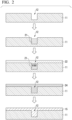
FIG. 1 is a flowchart showing a method of manufacturing a metal compound film according to one embodiment of the present invention. -
FIG. 2 is an explanatory view showing the method of manufacturing a metal compound film according to one embodiment of the present invention. - Hereinafter, a method of manufacturing a metal compound film according to an embodiment of the present invention will be described.
- In the method of manufacturing a metal compound film according to the present embodiment, for example, a metal compound film that is deposited on a surface of a substrate such as a semiconductor wafer and used as a hard mask during an etching treatment is targeted.
- In the present embodiment, depositing a metal oxide film that is a type of metal compound film will be described. In addition, in the present embodiment, using a sol-gel solution containing a metal oxide as a compound generating liquid (compound forming liquid) will be described.
- In the method of manufacturing a metal compound film according to the present embodiment, as shown in
FIG. 2 , ametal oxide film 15 is deposited on asubstrate 11 whose surface has anopening portion 12 such as a trench of a hole formed thereon. - Here, in the present embodiment, the
opening portion 12 is formed of a trench (groove) having an opening width of 10 nm or greater and 3 µm or less and a depth of 5 nm or greater and 500 nm or less. - Examples of the
substrate 11 include a silicon substrate, a sapphire substrate, and a GaN substrate. In the present embodiment, a silicon substrate is used. - In addition, the metal oxide constituting the
metal oxide film 15 is not particularly limited, and various metal oxides can be applied. However, in the present embodiment, any one or more of aluminum oxide, hafnium oxide, zirconium oxide, tungsten oxide, and titanium oxide are contained. - The
metal oxide film 15 is deposited by sintering a sol-gel solution 22 containing a metal oxide. - In addition, the method of manufacturing a metal compound film according to the present embodiment includes, as shown in
FIGS. 1 and2 : a pre-wet liquid application step S01 in which apre-wet liquid 21 having better wettability to thesubstrate 11 than the sol-gel solution 22 is applied to a surface of thesubstrate 11 and theopening portion 12 is filled with thepre-wet liquid 21; a sol-gel solution application step S02 in which the sol-gel solution 22 is applied to be stacked on thepre-wet liquid 21 on thesubstrate 11 and the solute component of the sol-gel solution 22 is diffused in thepre-wet liquid 21; a drying step S03 in which the applied sol-gel solution 22 is dried to form a metaloxide gel film 24; and a sintering step S04 in which the metaloxide gel film 24 is sintered and themetal oxide film 15 is formed. The contact angle of thepre-wet liquid 21 with respect to thesubstrate 11 is smaller than the contact angle of the sol-gel solution 22 with respect to thesubstrate 11. The contact angle of thepre-wet liquid 21 with respect to thesubstrate 11 is preferably 50° or less, and the contact angle of the sol-gel solution 22 with respect to thesubstrate 11 is preferably 80° or less. These contact angles are preferably small, that is, close to 0°. The contact angle of thepre-wet liquid 21 with respect to thesubstrate 11 can be adjusted to 1° or greater, and the contact angle of the sol-gel solution 22 with respect to thesubstrate 11 can be adjusted to 0° or greater. - In the pre-wet liquid application step 501, as described above, the
pre-wet liquid 21 having better wettability to thesubstrate 11 than the sol-gel solution 22 is applied, and thus theopening portion 12 formed on the surface of thesubstrate 11 is filled with thepre-wet liquid 21. As shown inFIG. 2 , theentire opening portion 12 may not be filled with thepre-wet liquid 21, and at least a bottom region of theopening portion 12 may be sufficiently wetted with thepre-wet liquid 21. - Purer water, an alcohol having 4 or less carbon atoms such as ethanol, an alcohol having an ether bond such as propylene glycol monomethyl ether (PGME), or the like is preferably used as the
pre-wet liquid 21. - In addition, in the pre-wet liquid application step S01, the
pre-wet liquid 21 is preferably applied by a spin coating method. It is possible to sufficiently fill theopening portion 12 with thepre-wet liquid 21 by applying the spin coating method. - Furthermore, the
pre-wet liquid 21 is preferably applied as a supercritical fluid at a temperature above a critical temperature and a pressure above a critical pressure. Since the supercritical fluid has particularly excellent wettability, it is possible to sufficiently fill theopening portion 12 with thepre-wet liquid 21. - In the sol-gel solution application step S02, as described above, the sol-
gel solution 22 is applied to be stacked on thepre-wet liquid 21 on thesubstrate 11 and the solute component of the sol-gel solution 22 is diffused in thepre-wet liquid 21. The sol-gel solution 22 can also be applied by the spin coating method. Accordingly, the openingportion 12 is also sufficiently filled with the solute component of the sol-gel solution 22. For example, the solute component of the sol-gel solution 22 is diffused in thepre-wet liquid 21 by being left for 5 seconds to 10 seconds. - In the present embodiment, the sol-
gel solution 22 contains, as the solute component, one or more selected from aluminum alkoxide, hafnium alkoxide, zirconium alkoxide, tungsten alkoxide, and silicon alkoxide, for example. In addition, examples of the solvent of the sol-gel solution 22 include ethanol, 1-butanol, and PGME. - In the drying step S03, the
substrate 11 to which thepre-wet liquid 21 and the sol-gel solution 22 have been applied is heated and dried to form the metaloxide gel film 24. As described above, since the openingportion 12 is filled with the solute component of the sol-gel solution 22, the openingportion 12 becomes filled with the metal oxide gel. - It is preferable that the heating in the drying step S03 be performed under conditions of an air atmosphere, a heating temperature of 50°C or higher and 300°C or lower, and a retention time of 1 minute or longer and 10 minutes or shorter at the heating temperature.
- Here, by repeatedly performing the sol-gel solution application step S02 and the drying step S03, the metal
oxide gel film 24 having a predetermined thickness is formed. - In a case where the opening
portion 12 is not filled after the drying step S03, the pre-wet liquid application step S01, the sol-gel solution application step S02, and the drying step S03 may be repeatedly performed. In a case when the steps are repeated, it is not necessary to perform the pre-wet liquid application step S01 for the second time and thereafter. - In the sintering step S04, the metal
oxide gel film 24 is sintered by being heated, and thus themetal oxide film 15 is formed. As described above, since the openingportion 12 is filled with the metal oxide gel, the openingportion 12 becomes filled with the metal oxide. - It is preferable that the heating in the sintering step S04 be performed under conditions of an air atmosphere or an oxygen atmosphere, a heating temperature of 400°C or higher and 800°C or lower, and a retention time of 3 minutes or longer and 10 minutes or shorter at the heating temperature.
- In a case where the sol-gel solution application step S02 and the drying step S03 are repeated, the sintering step S04 may be performed after each drying step S03.
- Through the above steps, the
metal oxide film 15 according to the present embodiment is manufactured. - In the method of manufacturing a metal compound film according to the present embodiment configured as described above, since the
pre-wet liquid 21 having better wettability to thesubstrate 11 than the sol-gel solution 22 is applied to the surface of thesubstrate 11 in the pre-wet liquid application step S01, it is possible to sufficiently fill theopening portion 12 on the surface of thesubstrate 11 with thepre-wet liquid 21. - In addition, in the sol-gel solution application step S02, since the sol-
gel solution 22 is applied in a state in which theopening portion 12 of thesubstrate 11 is filled with thepre-wet liquid 21, the solute component of the sol-gel solution 22 is diffused in thepre-wet liquid 21, and the openingportion 12 of thesubstrate 11 is filled with the solute component of the sol-gel. - In this state, by performing the drying step S03 and the sintering step S04, it is possible to deposit the
metal oxide film 15 having few voids, in which theopening portion 12 of thesubstrate 11 is filled with the metal oxide. - In the present embodiment, with a configuration in which the
pre-wet liquid 21 is applied by a spin coating method in the pre-wet liquid application step S01, it is possible to sufficiently fill theopening portion 12 of thesubstrate 11 with thepre-wet liquid 21. Accordingly, the openingportion 12 of thesubstrate 11 can be reliably filled with the metal oxide, and themetal oxide film 15 having few voids can be deposited. - In the present embodiment, in a case where the
pre-wet liquid 21 is applied as a supercritical fluid at a temperature above a critical temperature and a pressure above a critical pressure in the pre-wet liquid application step S01, the wettability between thepre-wet liquid 21 and thesubstrate 11 is further improved and it is possible to sufficiently fill theopening portion 12 of thesubstrate 11 with thepre-wet liquid 21. Accordingly, the openingportion 12 of thesubstrate 11 can be reliably filled with the metal oxide, and themetal oxide film 15 having few voids can be deposited. - The embodiments of the present invention have been described as above, but the present invention is not limited thereto, and can be appropriately changed without departing from the technical ideas of the present invention.
- In the present embodiment, the deposition of the metal oxide film that is a type of metal compound film using the sol-gel solution containing a metal oxide as a compound forming liquid has been described. However, the present invention is not limited thereto, and the metal compound film may be a metal nitride film or a metal oxynitride film. For example, in the deposition of a silicon nitride film that is a type of metal nitride film or a silicon oxynitride film that is a type of metal oxynitride film, a compound forming liquid containing polysilazane or the like as a solute component is used.
- According to the present invention, it is possible to provide a method of manufacturing a metal compound film in which in the deposition of a metal compound film on a substrate having an opening portion on a surface, the opening portion can be filled with a metal compound, and a metal compound film having few voids can thus be efficiently deposited.
-
- 11: Substrate
- 12: Opening portion
- 15: Metal oxide film (metal compound film)
- 21: Pre-wet liquid
- 22: Sol-gel solution (compound forming liquid)
- 24: Metal oxide gel film
- S01: Pre-wet liquid application step
- S02: Sol-gel solution application step (compound generating liquid application step)
- S03: Drying step
- S04: Sintering step
Claims (4)
- A method of manufacturing a metal compound film in which a compound generating liquid containing, as a solute component, a substance that generates a metal compound is applied to a substrate having an opening portion on a surface and sintered to form a metal compound film, the method comprising:a pre-wet liquid application step of applying a pre-wet liquid to the surface of the substrate, and filling the opening portion with the pre-wet liquid, the pre-wet liquid having better wettability to the substrate than the compound generating liquid;a compound generating liquid application step of applying the compound generating liquid to stack the compound generating liquid on the pre-wet liquid on the substrate, and diffusing the solute component of the compound generating liquid in the pre-wet liquid; anda sintering step of sintering the applied compound generating liquid to form the metal compound film.
- The method of manufacturing a metal compound film according to Claim 1,wherein the compound generating liquid is a sol-gel solution, anda drying step of drying the applied compound generating liquid to form a metal compound gel film, anda sintering step of sintering the metal compound gel film to form the metal compound film are provided.
- The method of manufacturing a metal compound film according to Claim 1 or 2,
wherein in the pre-wet liquid application step, the pre-wet liquid is applied by a spin coating method. - The method of manufacturing a metal compound film according to Claim 1 or 2,
wherein in the pre-wet liquid application step, the pre-wet liquid is a supercritical fluid.
Applications Claiming Priority (3)
| Application Number | Priority Date | Filing Date | Title |
|---|---|---|---|
| JP2021089729 | 2021-05-28 | ||
| JP2022086014A JP2022183110A (en) | 2021-05-28 | 2022-05-26 | Metal compound film manufacturing method |
| PCT/JP2022/021802 WO2022250151A1 (en) | 2021-05-28 | 2022-05-27 | Metal compound film production method |
Publications (2)
| Publication Number | Publication Date |
|---|---|
| EP4350745A1 true EP4350745A1 (en) | 2024-04-10 |
| EP4350745A4 EP4350745A4 (en) | 2025-07-30 |
Family
ID=84228927
Family Applications (1)
| Application Number | Title | Priority Date | Filing Date |
|---|---|---|---|
| EP22811419.5A Pending EP4350745A4 (en) | 2021-05-28 | 2022-05-27 | METHOD FOR PRODUCING METAL COMPOUND FILM |
Country Status (4)
| Country | Link |
|---|---|
| US (1) | US20240261818A1 (en) |
| EP (1) | EP4350745A4 (en) |
| TW (1) | TW202313209A (en) |
| WO (1) | WO2022250151A1 (en) |
Family Cites Families (10)
| Publication number | Priority date | Publication date | Assignee | Title |
|---|---|---|---|---|
| JPH05123632A (en) * | 1991-10-31 | 1993-05-21 | Canon Inc | Liquid coating substance coating method |
| JP3280225B2 (en) * | 1996-03-04 | 2002-04-30 | セントラル硝子株式会社 | Sol-gel thin film deposition method |
| JP4049841B2 (en) | 1996-12-27 | 2008-02-20 | Azエレクトロニックマテリアルズ株式会社 | Method for forming silicon nitride thin film |
| JP4680824B2 (en) * | 2006-04-21 | 2011-05-11 | 日立マクセル株式会社 | Method for forming plated film of polymer substrate and polymer substrate |
| JP4745358B2 (en) * | 2008-03-04 | 2011-08-10 | 株式会社東芝 | Spin coating method and spin coating apparatus |
| JP6017256B2 (en) | 2012-10-11 | 2016-10-26 | メルクパフォーマンスマテリアルズマニュファクチャリング合同会社 | Method for forming silicon dense film |
| NL2014598B1 (en) * | 2015-04-08 | 2017-01-20 | Suss Microtec Lithography Gmbh | Method for coating a substrate. |
| US10141183B2 (en) * | 2016-01-28 | 2018-11-27 | Tokyo Electron Limited | Methods of spin-on deposition of metal oxides |
| TWI712355B (en) | 2019-12-03 | 2020-12-01 | 和碩聯合科技股份有限公司 | Multi machinie body device |
| JP7092854B2 (en) | 2020-11-30 | 2022-06-28 | 株式会社ユニバーサルエンターテインメント | Pachinko machine |
-
2022
- 2022-05-27 WO PCT/JP2022/021802 patent/WO2022250151A1/en not_active Ceased
- 2022-05-27 US US18/564,132 patent/US20240261818A1/en not_active Abandoned
- 2022-05-27 TW TW111119914A patent/TW202313209A/en unknown
- 2022-05-27 EP EP22811419.5A patent/EP4350745A4/en active Pending
Also Published As
| Publication number | Publication date |
|---|---|
| EP4350745A4 (en) | 2025-07-30 |
| US20240261818A1 (en) | 2024-08-08 |
| TW202313209A (en) | 2023-04-01 |
| WO2022250151A1 (en) | 2022-12-01 |
Similar Documents
| Publication | Publication Date | Title |
|---|---|---|
| US8563076B2 (en) | Substrate structure and method of forming the same | |
| CN108352300B (en) | Semiconductor device processing method, system and apparatus | |
| KR20190101893A (en) | Method for deposition and reflow of a high quality etch resistant gapfill dielectric film | |
| US20100207203A1 (en) | Semiconductor device with buried gate and method for fabricating the same | |
| EP0973189A2 (en) | A method for gate-stack formation including a high-K dielectric | |
| EP1394286A1 (en) | Pretreatment of an organic layer for ALD thereof | |
| US6740248B2 (en) | Method for etching dielectric films | |
| US7582561B2 (en) | Method of selectively depositing materials on a substrate using a supercritical fluid | |
| TW201545233A (en) | Method of manufacturing an integrated circuit having an insulating layer | |
| WO2002058132A1 (en) | A method of filling trenches | |
| US7300855B2 (en) | Reversible oxidation protection of microcomponents | |
| US20100006957A1 (en) | Microscopic structure packaging method and device with packaged microscopic structure | |
| US6607984B1 (en) | Removable inorganic anti-reflection coating process | |
| US11600485B2 (en) | Using sacrificial solids in semiconductor processing | |
| US20240261818A1 (en) | Method of manufacturing metal compound film | |
| JP2022183110A (en) | Metal compound film manufacturing method | |
| JP5528430B2 (en) | Formation method of oxide layer | |
| US7214595B2 (en) | Method of producing semiconductor devices | |
| TWI239047B (en) | Use of masks made from metal oxides for the treatment of surfaces during the fabrication of microchips | |
| US11443947B2 (en) | Method for forming etching mask and method for manufacturing semiconductor device | |
| US7358187B2 (en) | Coating process for patterned substrate surfaces | |
| US20030094434A1 (en) | Passivation for cleaning a material | |
| US7479461B2 (en) | Method of etching silicon anisotropically | |
| JP2003258082A (en) | Method for manufacturing semiconductor device | |
| KR20210053178A (en) | Semiconductor device and method of manufacture |
Legal Events
| Date | Code | Title | Description |
|---|---|---|---|
| STAA | Information on the status of an ep patent application or granted ep patent |
Free format text: STATUS: THE INTERNATIONAL PUBLICATION HAS BEEN MADE |
|
| PUAI | Public reference made under article 153(3) epc to a published international application that has entered the european phase |
Free format text: ORIGINAL CODE: 0009012 |
|
| STAA | Information on the status of an ep patent application or granted ep patent |
Free format text: STATUS: REQUEST FOR EXAMINATION WAS MADE |
|
| 17P | Request for examination filed |
Effective date: 20231127 |
|
| AK | Designated contracting states |
Kind code of ref document: A1 Designated state(s): AL AT BE BG CH CY CZ DE DK EE ES FI FR GB GR HR HU IE IS IT LI LT LU LV MC MK MT NL NO PL PT RO RS SE SI SK SM TR |
|
| DAV | Request for validation of the european patent (deleted) | ||
| DAX | Request for extension of the european patent (deleted) | ||
| REG | Reference to a national code |
Ref country code: DE Ref legal event code: R079 Free format text: PREVIOUS MAIN CLASS: H01L0021316000 Ipc: H01L0021020000 |
|
| A4 | Supplementary search report drawn up and despatched |
Effective date: 20250702 |
|
| RIC1 | Information provided on ipc code assigned before grant |
Ipc: H01L 21/02 20060101AFI20250626BHEP Ipc: H01L 21/316 20060101ALI20250626BHEP |
|
| STAA | Information on the status of an ep patent application or granted ep patent |
Free format text: STATUS: THE APPLICATION IS DEEMED TO BE WITHDRAWN |