EP4350401A1 - Light source module - Google Patents
Light source module Download PDFInfo
- Publication number
- EP4350401A1 EP4350401A1 EP22811362.7A EP22811362A EP4350401A1 EP 4350401 A1 EP4350401 A1 EP 4350401A1 EP 22811362 A EP22811362 A EP 22811362A EP 4350401 A1 EP4350401 A1 EP 4350401A1
- Authority
- EP
- European Patent Office
- Prior art keywords
- light
- light emitter
- waveguide
- cladding
- source module
- Prior art date
- Legal status (The legal status is an assumption and is not a legal conclusion. Google has not performed a legal analysis and makes no representation as to the accuracy of the status listed.)
- Withdrawn
Links
Images


Classifications
-
- G—PHYSICS
- G02—OPTICS
- G02B—OPTICAL ELEMENTS, SYSTEMS OR APPARATUS
- G02B6/00—Light guides; Structural details of arrangements comprising light guides and other optical elements, e.g. couplings
- G02B6/24—Coupling light guides
- G02B6/26—Optical coupling means
- G02B6/28—Optical coupling means having data bus means, i.e. plural waveguides interconnected and providing an inherently bidirectional system by mixing and splitting signals
- G02B6/2804—Optical coupling means having data bus means, i.e. plural waveguides interconnected and providing an inherently bidirectional system by mixing and splitting signals forming multipart couplers without wavelength selective elements, e.g. "T" couplers, star couplers
- G02B6/2821—Optical coupling means having data bus means, i.e. plural waveguides interconnected and providing an inherently bidirectional system by mixing and splitting signals forming multipart couplers without wavelength selective elements, e.g. "T" couplers, star couplers using lateral coupling between contiguous fibres to split or combine optical signals
-
- G—PHYSICS
- G02—OPTICS
- G02B—OPTICAL ELEMENTS, SYSTEMS OR APPARATUS
- G02B6/00—Light guides; Structural details of arrangements comprising light guides and other optical elements, e.g. couplings
- G02B6/0001—Light guides; Structural details of arrangements comprising light guides and other optical elements, e.g. couplings specially adapted for lighting devices or systems
- G02B6/0005—Light guides; Structural details of arrangements comprising light guides and other optical elements, e.g. couplings specially adapted for lighting devices or systems the light guides being of the fibre type
- G02B6/0006—Coupling light into the fibre
-
- G—PHYSICS
- G02—OPTICS
- G02B—OPTICAL ELEMENTS, SYSTEMS OR APPARATUS
- G02B6/00—Light guides; Structural details of arrangements comprising light guides and other optical elements, e.g. couplings
- G02B6/0001—Light guides; Structural details of arrangements comprising light guides and other optical elements, e.g. couplings specially adapted for lighting devices or systems
- G02B6/0005—Light guides; Structural details of arrangements comprising light guides and other optical elements, e.g. couplings specially adapted for lighting devices or systems the light guides being of the fibre type
- G02B6/0008—Light guides; Structural details of arrangements comprising light guides and other optical elements, e.g. couplings specially adapted for lighting devices or systems the light guides being of the fibre type the light being emitted at the end of the fibre
-
- G—PHYSICS
- G02—OPTICS
- G02B—OPTICAL ELEMENTS, SYSTEMS OR APPARATUS
- G02B6/00—Light guides; Structural details of arrangements comprising light guides and other optical elements, e.g. couplings
- G02B6/10—Light guides; Structural details of arrangements comprising light guides and other optical elements, e.g. couplings of the optical waveguide type
- G02B6/12—Light guides; Structural details of arrangements comprising light guides and other optical elements, e.g. couplings of the optical waveguide type of the integrated circuit kind
- G02B6/122—Basic optical elements, e.g. light-guiding paths
- G02B6/125—Bends, branchings or intersections
-
- G—PHYSICS
- G02—OPTICS
- G02B—OPTICAL ELEMENTS, SYSTEMS OR APPARATUS
- G02B6/00—Light guides; Structural details of arrangements comprising light guides and other optical elements, e.g. couplings
- G02B6/24—Coupling light guides
- G02B6/42—Coupling light guides with opto-electronic elements
-
- G—PHYSICS
- G03—PHOTOGRAPHY; CINEMATOGRAPHY; ANALOGOUS TECHNIQUES USING WAVES OTHER THAN OPTICAL WAVES; ELECTROGRAPHY; HOLOGRAPHY
- G03B—APPARATUS OR ARRANGEMENTS FOR TAKING PHOTOGRAPHS OR FOR PROJECTING OR VIEWING THEM; APPARATUS OR ARRANGEMENTS EMPLOYING ANALOGOUS TECHNIQUES USING WAVES OTHER THAN OPTICAL WAVES; ACCESSORIES THEREFOR
- G03B21/00—Projectors or projection-type viewers; Accessories therefor
- G03B21/14—Details
- G03B21/20—Lamp housings
- G03B21/2006—Lamp housings characterised by the light source
- G03B21/2013—Plural light sources
-
- G—PHYSICS
- G03—PHOTOGRAPHY; CINEMATOGRAPHY; ANALOGOUS TECHNIQUES USING WAVES OTHER THAN OPTICAL WAVES; ELECTROGRAPHY; HOLOGRAPHY
- G03B—APPARATUS OR ARRANGEMENTS FOR TAKING PHOTOGRAPHS OR FOR PROJECTING OR VIEWING THEM; APPARATUS OR ARRANGEMENTS EMPLOYING ANALOGOUS TECHNIQUES USING WAVES OTHER THAN OPTICAL WAVES; ACCESSORIES THEREFOR
- G03B21/00—Projectors or projection-type viewers; Accessories therefor
- G03B21/14—Details
- G03B21/20—Lamp housings
- G03B21/2046—Positional adjustment of light sources
-
- H—ELECTRICITY
- H01—ELECTRIC ELEMENTS
- H01S—DEVICES USING THE PROCESS OF LIGHT AMPLIFICATION BY STIMULATED EMISSION OF RADIATION [LASER] TO AMPLIFY OR GENERATE LIGHT; DEVICES USING STIMULATED EMISSION OF ELECTROMAGNETIC RADIATION IN WAVE RANGES OTHER THAN OPTICAL
- H01S5/00—Semiconductor lasers
- H01S5/02—Structural details or components not essential to laser action
- H01S5/022—Mountings; Housings
- H01S5/0225—Out-coupling of light
-
- H—ELECTRICITY
- H01—ELECTRIC ELEMENTS
- H01S—DEVICES USING THE PROCESS OF LIGHT AMPLIFICATION BY STIMULATED EMISSION OF RADIATION [LASER] TO AMPLIFY OR GENERATE LIGHT; DEVICES USING STIMULATED EMISSION OF ELECTROMAGNETIC RADIATION IN WAVE RANGES OTHER THAN OPTICAL
- H01S5/00—Semiconductor lasers
- H01S5/02—Structural details or components not essential to laser action
- H01S5/022—Mountings; Housings
- H01S5/023—Mount members, e.g. sub-mount members
- H01S5/02325—Mechanically integrated components on mount members or optical micro-benches
-
- H—ELECTRICITY
- H01—ELECTRIC ELEMENTS
- H01S—DEVICES USING THE PROCESS OF LIGHT AMPLIFICATION BY STIMULATED EMISSION OF RADIATION [LASER] TO AMPLIFY OR GENERATE LIGHT; DEVICES USING STIMULATED EMISSION OF ELECTROMAGNETIC RADIATION IN WAVE RANGES OTHER THAN OPTICAL
- H01S5/00—Semiconductor lasers
- H01S5/40—Arrangement of two or more semiconductor lasers, not provided for in groups H01S5/02 - H01S5/30
- H01S5/4012—Beam combining, e.g. by the use of fibres, gratings, polarisers, prisms
-
- H—ELECTRICITY
- H01—ELECTRIC ELEMENTS
- H01S—DEVICES USING THE PROCESS OF LIGHT AMPLIFICATION BY STIMULATED EMISSION OF RADIATION [LASER] TO AMPLIFY OR GENERATE LIGHT; DEVICES USING STIMULATED EMISSION OF ELECTROMAGNETIC RADIATION IN WAVE RANGES OTHER THAN OPTICAL
- H01S5/00—Semiconductor lasers
- H01S5/02—Structural details or components not essential to laser action
- H01S5/022—Mountings; Housings
- H01S5/0225—Out-coupling of light
- H01S5/02253—Out-coupling of light using lenses
-
- H—ELECTRICITY
- H01—ELECTRIC ELEMENTS
- H01S—DEVICES USING THE PROCESS OF LIGHT AMPLIFICATION BY STIMULATED EMISSION OF RADIATION [LASER] TO AMPLIFY OR GENERATE LIGHT; DEVICES USING STIMULATED EMISSION OF ELECTROMAGNETIC RADIATION IN WAVE RANGES OTHER THAN OPTICAL
- H01S5/00—Semiconductor lasers
- H01S5/06—Arrangements for controlling the laser output parameters, e.g. by operating on the active medium
- H01S5/068—Stabilisation of laser output parameters
- H01S5/0683—Stabilisation of laser output parameters by monitoring the optical output parameters
-
- H—ELECTRICITY
- H01—ELECTRIC ELEMENTS
- H01S—DEVICES USING THE PROCESS OF LIGHT AMPLIFICATION BY STIMULATED EMISSION OF RADIATION [LASER] TO AMPLIFY OR GENERATE LIGHT; DEVICES USING STIMULATED EMISSION OF ELECTROMAGNETIC RADIATION IN WAVE RANGES OTHER THAN OPTICAL
- H01S5/00—Semiconductor lasers
- H01S5/10—Construction or shape of the optical resonator, e.g. extended or external cavity, coupled cavities, bent-guide, varying width, thickness or composition of the active region
- H01S5/1028—Coupling to elements in the cavity, e.g. coupling to waveguides adjacent the active region, e.g. forward coupled [DFC] structures
- H01S5/1032—Coupling to elements comprising an optical axis that is not aligned with the optical axis of the active region
-
- H—ELECTRICITY
- H01—ELECTRIC ELEMENTS
- H01S—DEVICES USING THE PROCESS OF LIGHT AMPLIFICATION BY STIMULATED EMISSION OF RADIATION [LASER] TO AMPLIFY OR GENERATE LIGHT; DEVICES USING STIMULATED EMISSION OF ELECTROMAGNETIC RADIATION IN WAVE RANGES OTHER THAN OPTICAL
- H01S5/00—Semiconductor lasers
- H01S5/40—Arrangement of two or more semiconductor lasers, not provided for in groups H01S5/02 - H01S5/30
- H01S5/4025—Array arrangements, e.g. constituted by discrete laser diodes or laser bar
-
- H—ELECTRICITY
- H01—ELECTRIC ELEMENTS
- H01S—DEVICES USING THE PROCESS OF LIGHT AMPLIFICATION BY STIMULATED EMISSION OF RADIATION [LASER] TO AMPLIFY OR GENERATE LIGHT; DEVICES USING STIMULATED EMISSION OF ELECTROMAGNETIC RADIATION IN WAVE RANGES OTHER THAN OPTICAL
- H01S5/00—Semiconductor lasers
- H01S5/40—Arrangement of two or more semiconductor lasers, not provided for in groups H01S5/02 - H01S5/30
- H01S5/4025—Array arrangements, e.g. constituted by discrete laser diodes or laser bar
- H01S5/4087—Array arrangements, e.g. constituted by discrete laser diodes or laser bar emitting more than one wavelength
- H01S5/4093—Red, green and blue [RGB] generated directly by laser action or by a combination of laser action with nonlinear frequency conversion
Definitions
- the present disclosure relates to a light source module.
- Patent Literature 1 A known technique is described in, for example, Patent Literature 1.
- Patent Literature 1 Japanese Unexamined Patent Application Publication No. 62-183405
- a light source module includes a first light emitter that emits light with a first wavelength, a second light emitter that emits light with a second wavelength different from the first wavelength, a third light emitter that emits light with a third wavelength different from the first wavelength and the second wavelength, a cladding, and a core in the cladding.
- the core includes a first waveguide that transmits light emitted from the first light emitter, a second waveguide that transmits light emitted from the second light emitter, a third waveguide that transmits light emitted from the third light emitter, a merging portion in which at least two waveguides of the first waveguide, the second waveguide, or the third waveguide merge, and an emission portion at one end of the merging portion.
- Each of the at least two waveguides includes a first portion that receives incident light and a second portion adjacent to the merging portion. The first portion has a greater width than the second portion.
- Patent Literature 1 describes an optical waveguide circuit including a tapered waveguide for such light source modules.
- a light source module is to cause light emitted from a light emitter to efficiently enter a waveguide.
- a light source module according to one or more embodiments of the present disclosure will now be described with reference to the accompanying drawings.
- the drawings used herein are schematic and are not drawn to scale relative to the actual size of each component.
- the light source module according to one or more embodiments of the present disclosure may be oriented with any sides being upward or downward, the light source module herein is defined using the orthogonal coordinate system (X, Y, and Z) for convenience, with its positive Z-direction being upward to have an upper surface or a lower surface.
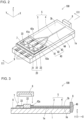
- FIG. 1 is an exploded perspective view of a light source module according to an embodiment of the present disclosure.
- FIG. 2 is a perspective view of the light source module in FIG. 1 without illustrating a lid.
- FIG. 3 is a cross-sectional view taken along line III-III in FIG. 2 .
- FIG. 4 is a plan view of the light source module in FIG. 1 .
- FIG. 5 is an end view taken along line V-V in FIG. 4 .
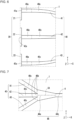
- FIGs. 6 and 7 are plan views of the light source module in FIG. 1 illustrating its main parts in an enlarged manner.
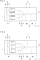
- FIG. 8 is a plan view of a light source module according to an embodiment of the present disclosure.
- FIG. 9 is a plan view of a light source module according to a variation of the embodiment of the present disclosure.
- FIG. 1 is an exploded perspective view of a light source module according to an embodiment of the present disclosure.
- FIG. 2 is a perspective view of the light source module in FIG. 1 without illustrating a lid.
- FIG. 2 is a perspective view as viewed in a direction different from FIG. 1 .
- FIG. 4 does not illustrate the lid.
- FIG. 6 is an enlarged view of part Ain FIG. 4 .
- FIG. 7 is an enlarged view of part B in FIG. 4 .
- FIGs. 6 and 7 illustrate a first light emitter, a second light emitter, a third light emitter, a core, and a substrate. The other components of the light source module are not illustrated in the figures.
- FIGs. 8 and 9 illustrate the first light emitter, the second light emitter, the third light emitter, a cladding, the core, and the substrate. The other components of the light source module are not illustrated in the figures.
- a light source module 100 includes a first light emitter 21, a second light emitter 22, a third light emitter 23, a cladding 3, and a core 4.
- the first light emitter 21, the second light emitter 22, and the third light emitter 23 may be, for example, semiconductor lasers or light-emitting diodes. In the example described below, the first light emitter 21, the second light emitter 22, and the third light emitter 23 are semiconductor lasers. The first light emitter 21, the second light emitter 22, and the third light emitter 23 may not be distinguished from one another and may be collectively referred to as light emitters 20.
- the first light emitter 21 emits light with a first wavelength at a peak of the light intensity.
- the second light emitter 22 emits light with a second wavelength at a peak of the light intensity.
- the third light emitter 23 emits light with a third wavelength at a peak of the light intensity.
- the first wavelength, the second wavelength, and the third wavelength differ from one another.
- the second wavelength may be, for example, longer than the first wavelength.
- the third wavelength may be, for example, longer than the second wavelength.
- the first wavelength may be in a wavelength region of about 400 to 500 nm.
- the first light emitter 21 that emits light in this wavelength region may be a blue semiconductor laser.
- the second wavelength may be in a wavelength region of about 500 to 600 nm.
- the second light emitter 22 that emits light in this wavelength region may be a green semiconductor laser.
- the third wavelength may be in a wavelength region of about 600 to 700 nm.
- the third light emitter 23 that emits light in this wavelength region may be a red semiconductor laser.
- the second wavelength is longer than the first wavelength
- the third wavelength is longer than the second wavelength.
- the first light emitter 21 is a blue semiconductor laser
- the second light emitter 22 is a green semiconductor laser
- the third light emitter 23 is a red semiconductor laser.
- the first light emitter 21 and the second light emitter 22 may each have, for example, a length of about 500 to 700 ⁇ m, a width of about 100 to 400 ⁇ m, and a height of about 50 to 150 ⁇ m.
- the third light emitter 23 may have, for example, a length of about 200 to 400 ⁇ m, a width of about 100 to 300 ⁇ m, and a height of about 50 to 150 ⁇ m.
- An optical waveguide layer 5 includes the cladding 3 and the core 4. As illustrated in, for example, FIGs. 1 to 5 , the core 4 is located in the cladding 3.
- the light source module 100 may include a substrate 1.
- the cladding 3 may be located on a first surface 1a of the substrate 1, and the core 4 may extend along the first surface 1a.
- the substrate 1 may be a ceramic wiring board made of a ceramic material.
- the ceramic material used for the ceramic wiring board include sintered aluminum oxide, sintered mullite, sintered silicon carbide, sintered aluminum nitride, and sintered glass ceramic.
- the ceramic wiring board may include conductors such as connection pads, internal wiring conductors, and external connection terminals for electrical connection between the light emitters 20 and an external circuit.
- the ceramic wiring board may be a stack.
- the substrate 1 may be an organic wiring board made of an organic material.
- the organic wiring board may be a printed wiring board, a build-up wiring board, or a flexible wiring board.
- Examples of the organic material used for the organic wiring board include an epoxy resin, a polyimide resin, a polyester resin, an acrylic resin, a phenolic resin, and a fluororesin.
- the organic wiring board may be a stack.
- the substrate 1 may be made of, for example, a compound semiconductor.
- the material used for the substrate made of the compound semiconductor include silicon (Si), germanium (Ge), gallium (Ga), arsenic (As), indium (In), phosphorus (P), and sapphire (Al 2 O 3 ).
- the optical waveguide layer 5 may be made of glass such as quartz, or a resin such as polymethyl methacrylate or a fluororesin.
- the cladding 3 and the core 4 in the optical waveguide layer 5 may be made of glass or a resin.
- one of the cladding 3 or the core 4 may be made of glass and the other may be made of a resin.
- the core 4 has a higher refractive index than the cladding 3.
- the optical waveguide layer 5 totally internally reflects light propagating through the core 4 using the cladding 3 and the core 4 with different refractive indexes.
- the optical waveguide layer 5 includes a path made of a material with a higher refractive index and surrounded by a material with a lower refractive index. The optical waveguide layer 5 can thus confine light inside the core 4 with the higher refractive index. Light propagates through the core 4 while being totally internally reflected repeatedly from the boundary between the core 4 and the cladding 3.
- the cladding 3 may include a lower cladding layer 31 and an upper cladding layer 32 stacked on each other.
- the core 4 may extend between the lower cladding layer 31 and the upper cladding layer 32.
- the upper cladding layer 32 may include, on its upper surface opposite to the lower surface facing the lower cladding layer 31, a ridge 32a in conformance with the core 4.
- the cladding 3 and the core 4 may have a refractive index difference of 0.05 to 0.30 between them.
- the optical waveguide layer 5 can stably transmit light in a multi-mode.
- the core 4 may have a constant dimension (height) in the height direction (Z-direction).
- the core 4 may have a height of about 1 to 5 ⁇ m.
- the optical waveguide layer 5 can be formed using techniques similar to, for example, photolithography and etching used in the semiconductor device manufacturing process.
- the core 4 includes a first waveguide 41, a second waveguide 42, and a third waveguide 43.
- the first waveguide 41 transmits light emitted from the first light emitter 21.
- the first waveguide 41 includes a first incident surface 41a that receives light emitted from the first light emitter 21.
- the first incident surface 41a faces a light emission surface of the first light emitter 21.
- the second waveguide 42 transmits light emitted from the second light emitter 22.
- the second waveguide 42 includes a second incident surface 42a that receives light emitted from the second light emitter 22.
- the second incident surface 42a faces a light emission surface of the second light emitter 22.
- the third waveguide 43 transmits light emitted from the third light emitter 23.
- the third waveguide 43 includes a third incident surface 43a that receives light emitted from the third light emitter 23.
- the third incident surface 43a faces a light emission surface of the third light emitter 23.
- the first waveguide 41, the second waveguide 42, and the third waveguide 43 may be hereafter collectively referred to as waveguides 40.
- the core 4 further includes a merging portion 44 and an emission portion 46. At least two of the first waveguide 41, the second waveguide 42, or the third waveguide 43 merge in the merging portion 44.
- the emission portion 46 is located at one end of the merging portion 44. As illustrated in, for example, FIGs. 1 to 4 , the emission portion 46 is located at one end of the merging portion 44 opposite to the waveguides 40. Light beams emitted from the light emitters 20 are combined in the merging portion 44 and are emitted outside through the emission portion 46.
- At least two waveguides merging in the merging portion 44 each include an incident portion 40a as a first portion and a pre-merging portion 40b as a second portion.
- the incident portion 40a receives light (also referred to as a beam) emitted from the corresponding light emitter.
- the incident portion 40a may have a constant width (or a fixed width).
- the incident portion 40a may have a length of about 50 to 600 ⁇ m.
- the length of each portion of the waveguides 40 herein refers to the length in the direction of light propagation.
- the width of each portion of the waveguides 40 herein refers to the length perpendicular to the direction of light propagation in a plan view.
- the pre-merging portion 40b is adjacent to the merging portion 44, or more specifically, connecting with the merging portion 44.
- the pre-merging portion 40b may be upstream from and adjacent to the merging portion 44 or be a surface connecting with the merging portion 44.
- At least two waveguides merging in the merging portion 44 may include the pre-merging portions 40b with the same width. In this case, light beams from at least two waveguides merging in the merging portion 44 uniformly enter the merging portion 44.
- the pre-merging portions 40b in at least two waveguides merging in the merging portion 44 may have different widths.
- the light source module 100 includes the incident portions 40a with a greater width than the pre-merging portions 40b.
- Each incident portion 40a may have a width of about 5 to 10 ⁇ m or about 7 ⁇ m.
- Each pre-merging portion 40b may have a width of about 1.5 to 5 ⁇ m or about 3 ⁇ m.
- the wider incident portion 40a has a greater tolerance in a direction orthogonal to the central axis of the incident portion 40a and along the first surface 1a of the substrate 1 when the corresponding light emitter 20 is mounted on the substrate 1. This allows light emitted from the light emitters 20 to efficiently enter at least two waveguides.
- the narrower pre-merging portion 40b allows a beam entering the incident portion 40a to be shaped (e.g., a Gaussian beam with high beam characteristics) for projection onto, for example, a screen or other surfaces before entering the merging portion 44.
- At least two waveguides merging in the merging portion 44 may include a third portion 40c (also referred to as a tapered waveguide portion) between the incident portion 40a and the pre-merging portion 40b in the direction of light propagation.
- the tapered waveguide portion 40c may have a width gradually decreasing toward the pre-merging portion 40b.
- the tapered waveguide portion 40c may have the same width as the incident portion 40a at its end adjacent to the incident portion 40a, and the same width as the pre-merging portion 40b at its end adjacent to the pre-merging portion 40b.
- the incident portion 40a has a constant width
- the tapered waveguide portion 40c nearer the emission portion 46 than the incident portion 40a has a tapered width. This structure reduces the likelihood that a beam emitted through the emission portion 46 has an unstable shape resulting from misalignment between the emission surface of each light emitter 20 and the incident surface of the corresponding waveguide 40.
- At least two waveguides merging in the merging portion 44 each include the tapered waveguide portion 40c, and thus each have a cross-sectional area gradually decreasing on a plane perpendicular to the direction of light propagation. At least two waveguides merging in the merging portion 44 can reduce possible phase variations in beams from the light emitters 20 entering the incident portions 40a, thus allowing propagation of the beams with the same phase.
- the merging portion 44 may include a fourth portion (also referred to as a tapered merging portion) 44a.
- the tapered merging portion 44a may be adjacent to at least two waveguides merging in the merging portion 44.
- the tapered merging portion 44a may have a width gradually decreasing toward the emission portion 46. As illustrated in, for example, FIG. 7 , the tapered merging portion 44a may be symmetric with respect to a central axis CA of the tapered merging portion 44a. With this structure, light beams from at least two waveguides merging in the merging portion 44 uniformly enter the tapered merging portion 44a and efficiently propagate through the tapered merging portion 44a.
- the tapered merging portion 44a has a cross-sectional area gradually decreasing on a plane perpendicular to the direction of light propagation. This reduces possible phase variations in beams entering the tapered merging portion 44a, thus allowing propagation of the beams with the same phase.
- the tapered merging portion 44a may be, for example, isosceles trapezoidal, or substantially isosceles trapezoidal in a plan view.
- the tapered merging portion 44a may have a width of about 4 to 30 ⁇ m or about 6 to 9 ⁇ m at its end adjacent to the waveguides 40.
- the tapered merging portion 44a may have a width of about 1.5 to 5 ⁇ m or about 3 ⁇ m at its end adjacent to the emission portion 46.
- the tapered merging portion 44a may have a length of about 100 to 600 ⁇ m or about 150 to 350 ⁇ m.
- the merging portion 44 may include a fifth portion (also referred to as a pre-emission portion) 44b.
- the pre-emission portion 44b may be between the tapered merging portion 44a and the emission portion 46.
- the pre-emission portion 44b may have a constant width.
- the pre-emission portion 44b with a fixed width is less likely to cause variations in the beam phase.
- the light source module 100 can thus emit a beam suitable for projection onto, for example, a screen.
- the pre-emission portion 44b may have a width of about 1.5 to 5 ⁇ m or about 3 ⁇ m.
- the cladding 3 may include a second surface 3a that is a lower surface facing the substrate 1 and a third surface 3b that is an upper surface opposite to the second surface 3a.
- the cladding 3 may include three through-holes 33 extending from the third surface 3b through the second surface 3a.
- the first light emitter 21, the second light emitter 22, and the third light emitter 23 may be received in the respective three through-holes 33 as illustrated in, for example, FIG. 1 .
- the through-holes 33 may be sized to receive the first to third light emitters 21, 22, and 23, and thus to have minimum openings. This increases the rigidity of the cladding 3 and reduces deformation of the cladding 3 and the core 4 in the cladding 3.
- the inner side surfaces of the through-holes 33 including the incident surfaces 41a, 42a, and 43a of the core 4 have less deformation, thus allowing light emitted from the first to third light emitters 21, 22, and 23 to efficiently enter the core 4.
- the through-holes 33 may be sized and shaped to fit the profiles of the first to third light emitters 21, 22, and 23. The first to third light emitters 21, 22, and 23 are simply placed into the corresponding through-holes 33 for easy positioning.
- the through-holes 33 may be replaced by a single through-hole 34 as illustrated in, for example, FIG. 9 , rather than being formed for the respective emitters.
- the first light emitter 21, the second light emitter 22, and the third light emitter 23 may all be received in the single through-hole 34.
- the single through-hole 34 may have an opening including the openings of the three through-holes 33. This structure reduces the likelihood that each light emitter 20 strikes against the opening edge or the inner peripheral surface of the through-hole 34 when the light emitter 20 is mounted on the substrate 1, facilitating the process for mounting the light emitters 20.
- the first incident surface 41a, the second incident surface 42a, and the third incident surface 43a can be at the same positions in the through-holes 33 for the respective emitters and also in the single through-hole 34.
- the through-holes 33 for the respective emitters as illustrated in, for example, FIG. 8 , at least either the width (in Y-direction in the figure) or the length (in X-direction in the figure) of each through-hole 33 may be greater than the corresponding dimension of the light emitter 20. This reduces the likelihood that each light emitter 20 strikes against the opening edge or the inner peripheral surface of the corresponding through-hole 33 when the light emitter 20 is mounted on the substrate 1.
- the cladding 3 has higher rigidity than in the structure with a larger single through-hole 34.
- the light source module 100 may further include a lid 6, a seal ring 7, and a condenser lens 8.
- the lid 6 is located above the third surface 3b of the cladding 3 and covers the first light emitter 21, the second light emitter 22, and the third light emitter 23.
- the seal ring 7 is between the lid 6 and the cladding 3.
- the seal ring 7 is a continuous loop surrounding the openings of all the three through-holes 33 in a plan view. The seal ring 7 improves the airtightness of the space accommodating the light emitters 20.
- the lid 6 may be directly joined to the cladding by, for example, heating. However, the cladding 3 and the core 4 may deform under stress during heating. This may cause misalignment of the optical axes between the light emitters 20 and the core 4.
- the seal ring 7 surrounding the through-holes 33 increases the mechanical strength around the through-holes 33 and reduces deformation of the cladding 3 and the core 4. This reduces misalignment of the optical axes between the light emitters 20 and the core 4.
- This structure is also usable for the cladding 3 including the single through-hole 34 to more noticeably reduce deformation of the cladding 3 and the core 4.
- the lid 6 may be made of, for example, a glass material such as quartz, borosilicate glass, or sapphire.
- the lid 6 may be made of a compound semiconductor such as silicon, a metal such as Fe, Ni, or Co, or an alloy of any of these metals.
- the seal ring 7 may be made of, for example, a metal such as Ti, Ni, Au, Pt, or Cr or an alloy of any of these metals.
- the seal ring 7 is fixed to the third surface 3b of the cladding 3 by, for example, vapor deposition, sputtering, ion plating, or plating.
- the lid 6 may be joined to the seal ring 7 by, for example, thermal curing or laser welding using a bond, such as Au-Sn or Sn-Ag-Cu solder, a metal nanoparticle paste of, for example, Ag or Cu, or a glass paste.
- a bond such as Au-Sn or Sn-Ag-Cu solder, a metal nanoparticle paste of, for example, Ag or Cu, or a glass paste.
- the seal ring 7 may be located on the lid 6, rather than on the cladding 3, in a portion facing the cladding 3.
- the seal ring 7 may be made of, for example, a metal such as Ti, Ni, Au, Pt, or Cr or an alloy of any of these metals.
- the seal ring 7 may be fixed to the lid 6 by, for example, vapor deposition, sputtering, ion plating, or plating.
- the cladding 3 may be joined to the seal ring 7 by, for example, thermal curing or laser welding using a bond, such as Au-Sn or Sn-Ag-Cu solder, a metal nanoparticle paste of, for example, Ag or Cu, or a glass paste.
- the seal ring 7 may be located on each of the cladding 3 and the lid 6.
- the seal ring 7 on the cladding 3 and the seal ring 7 on the lid 6 may be joined together by, for example, thermal curing or laser welding using a bond, such as Au-Sn or Sn-Ag-Cu solder, a metal nanoparticle paste of Ag or Cu, or a glass paste.
- the cladding 3 and the lid 6 may be joined together with high airtightness without any seal ring 7.
- the condenser lens 8 is located on the optical path of light emitted through the emission portion 46.
- the condenser lens 8 may collimate light emitted through the emission portion 46 or condense light emitted through the emission portions 46.
- the condenser lens 8 may be a plano-convex lens with an incident surface facing the emission portion 46 being flat and an emission surface being convex.
- the light source module 100 further includes multiple electrodes 9 for providing a drive current to the light emitters 20.
- two electrodes 9 are located for each of the first light emitter 21, the second light emitter 22, and the third light emitter 23 as illustrated in, for example, FIGs. 1 , 2 , and 4 .
- the two electrodes 9 may be two parallel wiring strips arranged on the first surface 1a of the substrate 1.
- each wiring strip may have one end located in an area surrounded by the inner peripheral surface of the corresponding through-hole 33 in the first surface 1a, and the other end exposed from the cladding 3 in the first surface 1a.
- Each wiring strip has one end electrically connected to the electrode (positive electrode or negative electrode) of the corresponding light emitter 20, and the other end electrically connected to an external power circuit.
- a light source module 100 includes a first light emitter 21 that emits light with a first wavelength, a second light emitter 22 that emits light with a second wavelength different from the first wavelength, and a third light emitter 23 that emits light with a third wavelength different from the first wavelength and the second wavelength, a cladding 3, and a core 4 in the cladding 3.
- the core 4 includes a first waveguide 41 that transmits light emitted from the first light emitter 21, a second waveguide 42 that transmits light emitted from the second light emitter 22, a third waveguide 43 that transmits light emitted from the third light emitter 23, a merging portion 44 in which at least two waveguides 40 of the first waveguide 41, the second waveguide 42, or the third waveguide 43 merge, and an emission portion 46 at one end of the merging portion 44.
- Each of the at least two waveguides 40 includes a first portion 40a that receives incident light and a second portion 40b adjacent to the merging portion 44.
- the first portion 40a has a greater width than the second portion 40b.
- the light source module 100 can efficiently allow light emitted from the light emitters 20 to enter the waveguides 40.
Landscapes
- Physics & Mathematics (AREA)
- General Physics & Mathematics (AREA)
- Optics & Photonics (AREA)
- Condensed Matter Physics & Semiconductors (AREA)
- Electromagnetism (AREA)
- Engineering & Computer Science (AREA)
- Microelectronics & Electronic Packaging (AREA)
- Semiconductor Lasers (AREA)
- Optical Integrated Circuits (AREA)
Abstract
Description
- The present disclosure relates to a light source module.
- A known technique is described in, for example,
Patent Literature 1. - Patent Literature 1:
Japanese Unexamined Patent Application Publication No. 62-183405 - In one or more aspects of the present disclosure, a light source module includes a first light emitter that emits light with a first wavelength, a second light emitter that emits light with a second wavelength different from the first wavelength, a third light emitter that emits light with a third wavelength different from the first wavelength and the second wavelength, a cladding, and a core in the cladding. The core includes a first waveguide that transmits light emitted from the first light emitter, a second waveguide that transmits light emitted from the second light emitter, a third waveguide that transmits light emitted from the third light emitter, a merging portion in which at least two waveguides of the first waveguide, the second waveguide, or the third waveguide merge, and an emission portion at one end of the merging portion. Each of the at least two waveguides includes a first portion that receives incident light and a second portion adjacent to the merging portion. The first portion has a greater width than the second portion.
-
-
FIG. 1 is an exploded perspective view of a light source module according to an embodiment of the present disclosure. -
FIG. 2 is a perspective view of the light source module inFIG. 1 without illustrating a lid. -
FIG. 3 is a cross-sectional view taken along line III-III inFIG. 2 . -
FIG. 4 is a plan view of the light source module inFIG. 1 . -
FIG. 5 is an end view taken along line V-V inFIG. 4 . -
FIG. 6 is a plan view of the light source module inFIG. 1 illustrating its main part in an enlarged manner. -
FIG. 7 is a plan view of the light source module inFIG. 1 illustrating its main part in an enlarged manner. -
FIG. 8 is a plan view of a light source module according to an embodiment of the present disclosure. -
FIG. 9 is a plan view of a light source module according to a variation of the embodiment of the present disclosure. - The objects, features, and advantages of the present disclosure will be more apparent from the following detailed description and the drawings.
- Various display devices and light source modules for display devices have been developed for projecting images onto, for example, a display screen using two-dimensional scanning of laser light.
Patent Literature 1 describes an optical waveguide circuit including a tapered waveguide for such light source modules. - A light source module is to cause light emitted from a light emitter to efficiently enter a waveguide.
- A light source module according to one or more embodiments of the present disclosure will now be described with reference to the accompanying drawings. The drawings used herein are schematic and are not drawn to scale relative to the actual size of each component. Although the light source module according to one or more embodiments of the present disclosure may be oriented with any sides being upward or downward, the light source module herein is defined using the orthogonal coordinate system (X, Y, and Z) for convenience, with its positive Z-direction being upward to have an upper surface or a lower surface.
-
FIG. 1 is an exploded perspective view of a light source module according to an embodiment of the present disclosure.FIG. 2 is a perspective view of the light source module inFIG. 1 without illustrating a lid.FIG. 3 is a cross-sectional view taken along line III-III inFIG. 2 .FIG. 4 is a plan view of the light source module inFIG. 1 .FIG. 5 is an end view taken along line V-V inFIG. 4 .FIGs. 6 and 7 are plan views of the light source module inFIG. 1 illustrating its main parts in an enlarged manner.FIG. 8 is a plan view of a light source module according to an embodiment of the present disclosure.FIG. 9 is a plan view of a light source module according to a variation of the embodiment of the present disclosure.FIG. 2 is a perspective view as viewed in a direction different fromFIG. 1 .FIG. 4 does not illustrate the lid.FIG. 6 is an enlarged view of part AinFIG. 4 .FIG. 7 is an enlarged view of part B inFIG. 4 .FIGs. 6 and 7 illustrate a first light emitter, a second light emitter, a third light emitter, a core, and a substrate. The other components of the light source module are not illustrated in the figures.FIGs. 8 and 9 illustrate the first light emitter, the second light emitter, the third light emitter, a cladding, the core, and the substrate. The other components of the light source module are not illustrated in the figures. - In the present embodiment, a
light source module 100 includes afirst light emitter 21, asecond light emitter 22, athird light emitter 23, acladding 3, and acore 4. - The
first light emitter 21, thesecond light emitter 22, and thethird light emitter 23 may be, for example, semiconductor lasers or light-emitting diodes. In the example described below, thefirst light emitter 21, thesecond light emitter 22, and thethird light emitter 23 are semiconductor lasers. Thefirst light emitter 21, thesecond light emitter 22, and thethird light emitter 23 may not be distinguished from one another and may be collectively referred to aslight emitters 20. - The
first light emitter 21 emits light with a first wavelength at a peak of the light intensity. Thesecond light emitter 22 emits light with a second wavelength at a peak of the light intensity. Thethird light emitter 23 emits light with a third wavelength at a peak of the light intensity. The first wavelength, the second wavelength, and the third wavelength differ from one another. - The second wavelength may be, for example, longer than the first wavelength. The third wavelength may be, for example, longer than the second wavelength. The first wavelength may be in a wavelength region of about 400 to 500 nm. The first light emitter 21 that emits light in this wavelength region may be a blue semiconductor laser. The second wavelength may be in a wavelength region of about 500 to 600 nm. The second light emitter 22 that emits light in this wavelength region may be a green semiconductor laser. The third wavelength may be in a wavelength region of about 600 to 700 nm. The third light emitter 23 that emits light in this wavelength region may be a red semiconductor laser. In the example below, the second wavelength is longer than the first wavelength, and the third wavelength is longer than the second wavelength. In this example, the
first light emitter 21 is a blue semiconductor laser, thesecond light emitter 22 is a green semiconductor laser, and thethird light emitter 23 is a red semiconductor laser. - The
first light emitter 21 and thesecond light emitter 22 may each have, for example, a length of about 500 to 700 µm, a width of about 100 to 400 µm, and a height of about 50 to 150 µm. Thethird light emitter 23 may have, for example, a length of about 200 to 400 µm, a width of about 100 to 300 µm, and a height of about 50 to 150 µm. - An
optical waveguide layer 5 includes thecladding 3 and thecore 4. As illustrated in, for example,FIGs. 1 to 5 , thecore 4 is located in thecladding 3. Thelight source module 100 may include asubstrate 1. In this case, thecladding 3 may be located on afirst surface 1a of thesubstrate 1, and thecore 4 may extend along thefirst surface 1a. - The
substrate 1 may be a ceramic wiring board made of a ceramic material. Examples of the ceramic material used for the ceramic wiring board include sintered aluminum oxide, sintered mullite, sintered silicon carbide, sintered aluminum nitride, and sintered glass ceramic. The ceramic wiring board may include conductors such as connection pads, internal wiring conductors, and external connection terminals for electrical connection between thelight emitters 20 and an external circuit. The ceramic wiring board may be a stack. - The
substrate 1 may be an organic wiring board made of an organic material. The organic wiring board may be a printed wiring board, a build-up wiring board, or a flexible wiring board. Examples of the organic material used for the organic wiring board include an epoxy resin, a polyimide resin, a polyester resin, an acrylic resin, a phenolic resin, and a fluororesin. The organic wiring board may be a stack. - The
substrate 1 may be made of, for example, a compound semiconductor. Examples of the material used for the substrate made of the compound semiconductor include silicon (Si), germanium (Ge), gallium (Ga), arsenic (As), indium (In), phosphorus (P), and sapphire (Al2O3). - The
optical waveguide layer 5 may be made of glass such as quartz, or a resin such as polymethyl methacrylate or a fluororesin. Thecladding 3 and thecore 4 in theoptical waveguide layer 5 may be made of glass or a resin. In some embodiments, one of thecladding 3 or thecore 4 may be made of glass and the other may be made of a resin. Thecore 4 has a higher refractive index than thecladding 3. Theoptical waveguide layer 5 totally internally reflects light propagating through thecore 4 using thecladding 3 and thecore 4 with different refractive indexes. Theoptical waveguide layer 5 includes a path made of a material with a higher refractive index and surrounded by a material with a lower refractive index. Theoptical waveguide layer 5 can thus confine light inside thecore 4 with the higher refractive index. Light propagates through thecore 4 while being totally internally reflected repeatedly from the boundary between thecore 4 and thecladding 3. - As illustrated in, for example,
FIG. 5 , thecladding 3 may include alower cladding layer 31 and anupper cladding layer 32 stacked on each other. Thecore 4 may extend between thelower cladding layer 31 and theupper cladding layer 32. Theupper cladding layer 32 may include, on its upper surface opposite to the lower surface facing thelower cladding layer 31, aridge 32a in conformance with thecore 4. - In the
optical waveguide layer 5, thecladding 3 and thecore 4 may have a refractive index difference of 0.05 to 0.30 between them. In this case, theoptical waveguide layer 5 can stably transmit light in a multi-mode. Thecore 4 may have a constant dimension (height) in the height direction (Z-direction). Thecore 4 may have a height of about 1 to 5 µm. Theoptical waveguide layer 5 can be formed using techniques similar to, for example, photolithography and etching used in the semiconductor device manufacturing process. - The
core 4 includes afirst waveguide 41, asecond waveguide 42, and athird waveguide 43. Thefirst waveguide 41 transmits light emitted from thefirst light emitter 21. Thefirst waveguide 41 includes afirst incident surface 41a that receives light emitted from thefirst light emitter 21. Thefirst incident surface 41a faces a light emission surface of thefirst light emitter 21. Thesecond waveguide 42 transmits light emitted from thesecond light emitter 22. Thesecond waveguide 42 includes asecond incident surface 42a that receives light emitted from thesecond light emitter 22. Thesecond incident surface 42a faces a light emission surface of thesecond light emitter 22. Thethird waveguide 43 transmits light emitted from thethird light emitter 23. Thethird waveguide 43 includes athird incident surface 43a that receives light emitted from thethird light emitter 23. Thethird incident surface 43a faces a light emission surface of thethird light emitter 23. Thefirst waveguide 41, thesecond waveguide 42, and thethird waveguide 43 may be hereafter collectively referred to aswaveguides 40. - The
core 4 further includes a mergingportion 44 and anemission portion 46. At least two of thefirst waveguide 41, thesecond waveguide 42, or thethird waveguide 43 merge in the mergingportion 44. Theemission portion 46 is located at one end of the mergingportion 44. As illustrated in, for example,FIGs. 1 to 4 , theemission portion 46 is located at one end of the mergingportion 44 opposite to thewaveguides 40. Light beams emitted from thelight emitters 20 are combined in the mergingportion 44 and are emitted outside through theemission portion 46. - At least two waveguides merging in the merging
portion 44 each include anincident portion 40a as a first portion and apre-merging portion 40b as a second portion. Theincident portion 40a receives light (also referred to as a beam) emitted from the corresponding light emitter. Theincident portion 40a may have a constant width (or a fixed width). Theincident portion 40a may have a length of about 50 to 600 µm. The length of each portion of thewaveguides 40 herein refers to the length in the direction of light propagation. The width of each portion of thewaveguides 40 herein refers to the length perpendicular to the direction of light propagation in a plan view. - The
pre-merging portion 40b is adjacent to the mergingportion 44, or more specifically, connecting with the mergingportion 44. Thepre-merging portion 40b may be upstream from and adjacent to the mergingportion 44 or be a surface connecting with the mergingportion 44. At least two waveguides merging in the mergingportion 44 may include thepre-merging portions 40b with the same width. In this case, light beams from at least two waveguides merging in the mergingportion 44 uniformly enter the mergingportion 44. To shape the combined light beams, thepre-merging portions 40b in at least two waveguides merging in the mergingportion 44 may have different widths. - The
light source module 100 includes theincident portions 40a with a greater width than thepre-merging portions 40b. Eachincident portion 40a may have a width of about 5 to 10 µm or about 7 µm. Eachpre-merging portion 40b may have a width of about 1.5 to 5 µm or about 3 µm. Thewider incident portion 40a has a greater tolerance in a direction orthogonal to the central axis of theincident portion 40a and along thefirst surface 1a of thesubstrate 1 when thecorresponding light emitter 20 is mounted on thesubstrate 1. This allows light emitted from thelight emitters 20 to efficiently enter at least two waveguides. The narrowerpre-merging portion 40b allows a beam entering theincident portion 40a to be shaped (e.g., a Gaussian beam with high beam characteristics) for projection onto, for example, a screen or other surfaces before entering the mergingportion 44. - At least two waveguides merging in the merging
portion 44 may include athird portion 40c (also referred to as a tapered waveguide portion) between theincident portion 40a and thepre-merging portion 40b in the direction of light propagation. The taperedwaveguide portion 40c may have a width gradually decreasing toward thepre-merging portion 40b. The taperedwaveguide portion 40c may have the same width as theincident portion 40a at its end adjacent to theincident portion 40a, and the same width as thepre-merging portion 40b at its end adjacent to thepre-merging portion 40b. Theincident portion 40a has a constant width, whereas the taperedwaveguide portion 40c nearer theemission portion 46 than theincident portion 40a has a tapered width. This structure reduces the likelihood that a beam emitted through theemission portion 46 has an unstable shape resulting from misalignment between the emission surface of eachlight emitter 20 and the incident surface of the correspondingwaveguide 40. - At least two waveguides merging in the merging
portion 44 each include the taperedwaveguide portion 40c, and thus each have a cross-sectional area gradually decreasing on a plane perpendicular to the direction of light propagation. At least two waveguides merging in the mergingportion 44 can reduce possible phase variations in beams from thelight emitters 20 entering theincident portions 40a, thus allowing propagation of the beams with the same phase. - The merging
portion 44 may include a fourth portion (also referred to as a tapered merging portion) 44a. The tapered mergingportion 44a may be adjacent to at least two waveguides merging in the mergingportion 44. The tapered mergingportion 44a may have a width gradually decreasing toward theemission portion 46. As illustrated in, for example,FIG. 7 , the tapered mergingportion 44a may be symmetric with respect to a central axis CA of the tapered mergingportion 44a. With this structure, light beams from at least two waveguides merging in the mergingportion 44 uniformly enter the tapered mergingportion 44a and efficiently propagate through the tapered mergingportion 44a. The tapered mergingportion 44a has a cross-sectional area gradually decreasing on a plane perpendicular to the direction of light propagation. This reduces possible phase variations in beams entering the tapered mergingportion 44a, thus allowing propagation of the beams with the same phase. - The tapered merging
portion 44a may be, for example, isosceles trapezoidal, or substantially isosceles trapezoidal in a plan view. The tapered mergingportion 44a may have a width of about 4 to 30 µm or about 6 to 9 µm at its end adjacent to thewaveguides 40. The tapered mergingportion 44a may have a width of about 1.5 to 5 µm or about 3 µm at its end adjacent to theemission portion 46. The tapered mergingportion 44a may have a length of about 100 to 600 µm or about 150 to 350 µm. - The merging
portion 44 may include a fifth portion (also referred to as a pre-emission portion) 44b. Thepre-emission portion 44b may be between the tapered mergingportion 44a and theemission portion 46. Thepre-emission portion 44b may have a constant width. Thepre-emission portion 44b with a fixed width is less likely to cause variations in the beam phase. Thelight source module 100 can thus emit a beam suitable for projection onto, for example, a screen. Thepre-emission portion 44b may have a width of about 1.5 to 5 µm or about 3 µm. - As illustrated in, for example,
FIG. 3 , thecladding 3 may include asecond surface 3a that is a lower surface facing thesubstrate 1 and athird surface 3b that is an upper surface opposite to thesecond surface 3a. Thecladding 3 may include three through-holes 33 extending from thethird surface 3b through thesecond surface 3a. Thefirst light emitter 21, thesecond light emitter 22, and thethird light emitter 23 may be received in the respective three through-holes 33 as illustrated in, for example,FIG. 1 . The through-holes 33 may be sized to receive the first to thirdlight emitters cladding 3 and reduces deformation of thecladding 3 and thecore 4 in thecladding 3. In particular, the inner side surfaces of the through-holes 33 including the incident surfaces 41a, 42a, and 43a of thecore 4 have less deformation, thus allowing light emitted from the first to thirdlight emitters core 4. As illustrated in, for example,FIG. 4 , the through-holes 33 may be sized and shaped to fit the profiles of the first to thirdlight emitters light emitters holes 33 for easy positioning. - The through-
holes 33 may be replaced by a single through-hole 34 as illustrated in, for example,FIG. 9 , rather than being formed for the respective emitters. Thefirst light emitter 21, thesecond light emitter 22, and thethird light emitter 23 may all be received in the single through-hole 34. The single through-hole 34 may have an opening including the openings of the three through-holes 33. This structure reduces the likelihood that eachlight emitter 20 strikes against the opening edge or the inner peripheral surface of the through-hole 34 when thelight emitter 20 is mounted on thesubstrate 1, facilitating the process for mounting thelight emitters 20. Thefirst incident surface 41a, thesecond incident surface 42a, and thethird incident surface 43a can be at the same positions in the through-holes 33 for the respective emitters and also in the single through-hole 34. For the through-holes 33 for the respective emitters, as illustrated in, for example,FIG. 8 , at least either the width (in Y-direction in the figure) or the length (in X-direction in the figure) of each through-hole 33 may be greater than the corresponding dimension of thelight emitter 20. This reduces the likelihood that eachlight emitter 20 strikes against the opening edge or the inner peripheral surface of the corresponding through-hole 33 when thelight emitter 20 is mounted on thesubstrate 1. In this case as well, thecladding 3 has higher rigidity than in the structure with a larger single through-hole 34. - As illustrated in, for example,
FIGs. 1 and3 , thelight source module 100 may further include alid 6, aseal ring 7, and acondenser lens 8. - The
lid 6 is located above thethird surface 3b of thecladding 3 and covers thefirst light emitter 21, thesecond light emitter 22, and thethird light emitter 23. Theseal ring 7 is between thelid 6 and thecladding 3. Theseal ring 7 is a continuous loop surrounding the openings of all the three through-holes 33 in a plan view. Theseal ring 7 improves the airtightness of the space accommodating thelight emitters 20. - The
lid 6 may be directly joined to the cladding by, for example, heating. However, thecladding 3 and thecore 4 may deform under stress during heating. This may cause misalignment of the optical axes between thelight emitters 20 and thecore 4. Theseal ring 7 surrounding the through-holes 33 increases the mechanical strength around the through-holes 33 and reduces deformation of thecladding 3 and thecore 4. This reduces misalignment of the optical axes between thelight emitters 20 and thecore 4. This structure is also usable for thecladding 3 including the single through-hole 34 to more noticeably reduce deformation of thecladding 3 and thecore 4. - The
lid 6 may be made of, for example, a glass material such as quartz, borosilicate glass, or sapphire. Thelid 6 may be made of a compound semiconductor such as silicon, a metal such as Fe, Ni, or Co, or an alloy of any of these metals. Theseal ring 7 may be made of, for example, a metal such as Ti, Ni, Au, Pt, or Cr or an alloy of any of these metals. Theseal ring 7 is fixed to thethird surface 3b of thecladding 3 by, for example, vapor deposition, sputtering, ion plating, or plating. Thelid 6 may be joined to theseal ring 7 by, for example, thermal curing or laser welding using a bond, such as Au-Sn or Sn-Ag-Cu solder, a metal nanoparticle paste of, for example, Ag or Cu, or a glass paste. - The
seal ring 7 may be located on thelid 6, rather than on thecladding 3, in a portion facing thecladding 3. Theseal ring 7 may be made of, for example, a metal such as Ti, Ni, Au, Pt, or Cr or an alloy of any of these metals. Theseal ring 7 may be fixed to thelid 6 by, for example, vapor deposition, sputtering, ion plating, or plating. Thecladding 3 may be joined to theseal ring 7 by, for example, thermal curing or laser welding using a bond, such as Au-Sn or Sn-Ag-Cu solder, a metal nanoparticle paste of, for example, Ag or Cu, or a glass paste. - The
seal ring 7 may be located on each of thecladding 3 and thelid 6. Theseal ring 7 on thecladding 3 and theseal ring 7 on thelid 6 may be joined together by, for example, thermal curing or laser welding using a bond, such as Au-Sn or Sn-Ag-Cu solder, a metal nanoparticle paste of Ag or Cu, or a glass paste. Thecladding 3 and thelid 6 may be joined together with high airtightness without anyseal ring 7. - The
condenser lens 8 is located on the optical path of light emitted through theemission portion 46. Thecondenser lens 8 may collimate light emitted through theemission portion 46 or condense light emitted through theemission portions 46. As illustrated in, for example,FIG. 3 , thecondenser lens 8 may be a plano-convex lens with an incident surface facing theemission portion 46 being flat and an emission surface being convex. - The
light source module 100 further includesmultiple electrodes 9 for providing a drive current to thelight emitters 20. In the present embodiment, twoelectrodes 9 are located for each of thefirst light emitter 21, thesecond light emitter 22, and thethird light emitter 23 as illustrated in, for example,FIGs. 1 ,2 , and4 . The twoelectrodes 9 may be two parallel wiring strips arranged on thefirst surface 1a of thesubstrate 1. In a plan view, each wiring strip may have one end located in an area surrounded by the inner peripheral surface of the corresponding through-hole 33 in thefirst surface 1a, and the other end exposed from thecladding 3 in thefirst surface 1a. Each wiring strip has one end electrically connected to the electrode (positive electrode or negative electrode) of thecorresponding light emitter 20, and the other end electrically connected to an external power circuit. - The present disclosure may be implemented in the following forms.
- In one or more embodiments of the present disclosure, a
light source module 100 includes afirst light emitter 21 that emits light with a first wavelength, asecond light emitter 22 that emits light with a second wavelength different from the first wavelength, and athird light emitter 23 that emits light with a third wavelength different from the first wavelength and the second wavelength, acladding 3, and acore 4 in thecladding 3. Thecore 4 includes afirst waveguide 41 that transmits light emitted from thefirst light emitter 21, asecond waveguide 42 that transmits light emitted from thesecond light emitter 22, athird waveguide 43 that transmits light emitted from thethird light emitter 23, a mergingportion 44 in which at least twowaveguides 40 of thefirst waveguide 41, thesecond waveguide 42, or thethird waveguide 43 merge, and anemission portion 46 at one end of the mergingportion 44. Each of the at least twowaveguides 40 includes afirst portion 40a that receives incident light and asecond portion 40b adjacent to the mergingportion 44. Thefirst portion 40a has a greater width than thesecond portion 40b. - In one or more embodiments of the present disclosure, the
light source module 100 can efficiently allow light emitted from thelight emitters 20 to enter thewaveguides 40. - Although embodiments of the present disclosure have been described in detail, the present disclosure is not limited to the embodiments described above, and may be changed or varied in various manners without departing from the spirit and scope of the present disclosure. The components described in the above embodiments may be entirely or partially combined as appropriate unless any contradiction arises.
-
- 100
- light source module
- 1
- substrate
- 1a
- one main surface (first surface)
- 3
- cladding
- 3a
- lower surface (second surface)
- 3b
- upper surface (third surface)
- 4
- core
- 5
- optical waveguide layer
- 6
- lid
- 7
- seal ring
- 8
- condenser lens
- 9
- electrode
- 20
- light emitter
- 21
- first light emitter
- 22
- second light emitter
- 23
- third light emitter
- 31
- lower cladding layer
- 32
- upper cladding layer
- 32a
- ridge
- 33, 34
- through-hole
- 40
- waveguide
- 40a
- first portion (incident portion)
- 40b
- second portion (pre-merging portion)
- 40c
- third portion (tapered waveguide portion)
- 41
- first waveguide
- 41a
- first incident surface
- 42
- second waveguide
- 42a
- second incident surface
- 43
- third waveguide
- 43a
- third incident surface
- 44
- merging portion
- 44a
- fourth portion (tapered merging portion)
- 44b
- fifth portion (pre-emission portion)
- 46
- emission portion
Claims (6)
- A light source module, comprising:a first light emitter configured to emit light with a first wavelength;a second light emitter configured to emit light with a second wavelength different from the first wavelength;a third light emitter configured to emit light with a third wavelength different from the first wavelength and the second wavelength;a cladding; anda core in the cladding, the core includinga first waveguide configured to transmit light emitted from the first light emitter,a second waveguide configured to transmit light emitted from the second light emitter,a third waveguide configured to transmit light emitted from the third light emitter,a merging portion in which at least two waveguides of the first waveguide, the second waveguide, or the third waveguide merge, andan emission portion at one end of the merging portion,wherein each of the at least two waveguides includes a first portion configured to receive incident light and a second portion adjacent to the merging portion, and the first portion has a greater width than the second portion.
- The light source module according to claim 1, whereinthe first portion of each of the at least two waveguides has a constant width, andeach of the at least two waveguides includes a third portion between the first portion and the second portion, and the third portion has a width gradually decreasing toward the second portion.
- The light source module according to claim 2, wherein
the merging portion includes a fourth portion adjacent to the at least two waveguides, and the fourth portion is symmetric with respect to a central axis of the fourth portion and has a width gradually decreasing toward the emission portion. - The light source module according to claim 3, wherein
the merging portion includes a fifth portion between the fourth portion and the emission portion, and the fifth portion has a constant width. - The light source module according to any one of claims 1 to 4, further comprising:a substrate including a first surface, the substrate receiving the first light emitter, the second light emitter, the third light emitter, and the cladding on the first surface;a lid above the first surface, the lid covering the first light emitter, the second light emitter, and the third light emitter; anda condenser lens on an optical path of light emitted through the emission portion.
- The light source module according to claim 5, whereinthe cladding includes a second surface facing the substrate, a third surface opposite to the second surface, and three through-holes extending from the second surface through the third surface, andthe first light emitter, the second light emitter, and the third light emitter are received in the respective three through-holes.
Applications Claiming Priority (2)
| Application Number | Priority Date | Filing Date | Title |
|---|---|---|---|
| JP2021090062 | 2021-05-28 | ||
| PCT/JP2022/021443 WO2022250092A1 (en) | 2021-05-28 | 2022-05-25 | Light source module |
Publications (2)
| Publication Number | Publication Date |
|---|---|
| EP4350401A1 true EP4350401A1 (en) | 2024-04-10 |
| EP4350401A4 EP4350401A4 (en) | 2025-04-30 |
Family
ID=84230128
Family Applications (1)
| Application Number | Title | Priority Date | Filing Date |
|---|---|---|---|
| EP22811362.7A Withdrawn EP4350401A4 (en) | 2021-05-28 | 2022-05-25 | LIGHT SOURCE MODULE |
Country Status (6)
| Country | Link |
|---|---|
| US (1) | US12292590B2 (en) |
| EP (1) | EP4350401A4 (en) |
| JP (1) | JPWO2022250092A1 (en) |
| CN (1) | CN117396785A (en) |
| TW (1) | TWI873424B (en) |
| WO (1) | WO2022250092A1 (en) |
Family Cites Families (13)
| Publication number | Priority date | Publication date | Assignee | Title |
|---|---|---|---|---|
| JPS62183405A (en) | 1986-02-08 | 1987-08-11 | Agency Of Ind Science & Technol | Optical waveguide circuit with taper and its production |
| DE10256365A1 (en) * | 2001-12-04 | 2003-07-17 | Ccs Inc | Light radiation device for testing semiconductor chip, has lens mounted on optical fibers in one-to-one correspondence and closer to light transmission end of optical fibers |
| KR20040017539A (en) * | 2002-08-22 | 2004-02-27 | 우리로광통신주식회사 | Three branching type optical waveguide |
| JP2005070573A (en) * | 2003-08-27 | 2005-03-17 | Sony Corp | Optical waveguide, light source module, and optical information processing apparatus |
| JP2005266657A (en) * | 2004-03-22 | 2005-09-29 | Sony Corp | Optical waveguide, optical waveguide device, and optical information processing apparatus |
| JP2006012888A (en) * | 2004-06-22 | 2006-01-12 | Fuji Photo Film Co Ltd | Combined laser light irradiation method and equipment thereof |
| JP2007041378A (en) * | 2005-08-04 | 2007-02-15 | Fujifilm Corp | Combined light source |
| WO2017090333A1 (en) * | 2015-11-27 | 2017-06-01 | シャープ株式会社 | Optical waveguide element and light source module |
| JP7187148B2 (en) * | 2017-12-13 | 2022-12-12 | 日東電工株式会社 | optical waveguide |
| JP2020194071A (en) * | 2019-05-28 | 2020-12-03 | 京セラ株式会社 | Optical waveguide and rgb light-emitting device |
| CN114424099A (en) * | 2019-09-30 | 2022-04-29 | 京瓷株式会社 | Optical waveguide package and light emitting device |
| EP4040517A4 (en) * | 2019-09-30 | 2023-10-25 | Kyocera Corporation | HOUSING FOR OPTICAL WAVE GUIDES AND LIGHT EMITTING DEVICE |
| US12512252B2 (en) | 2022-06-15 | 2025-12-30 | Analog Devices, Inc. | Monolithic or multi-die integrated circuit transformer |
-
2022
- 2022-05-25 EP EP22811362.7A patent/EP4350401A4/en not_active Withdrawn
- 2022-05-25 US US18/564,408 patent/US12292590B2/en active Active
- 2022-05-25 CN CN202280038118.6A patent/CN117396785A/en active Pending
- 2022-05-25 TW TW111119451A patent/TWI873424B/en active
- 2022-05-25 JP JP2023523510A patent/JPWO2022250092A1/ja active Pending
- 2022-05-25 WO PCT/JP2022/021443 patent/WO2022250092A1/en not_active Ceased
Also Published As
| Publication number | Publication date |
|---|---|
| CN117396785A (en) | 2024-01-12 |
| JPWO2022250092A1 (en) | 2022-12-01 |
| TW202305484A (en) | 2023-02-01 |
| US20240255686A1 (en) | 2024-08-01 |
| WO2022250092A1 (en) | 2022-12-01 |
| EP4350401A4 (en) | 2025-04-30 |
| US12292590B2 (en) | 2025-05-06 |
| TWI873424B (en) | 2025-02-21 |
Similar Documents
| Publication | Publication Date | Title |
|---|---|---|
| JP7528213B2 (en) | Optical waveguide package, light emitting device and projection system | |
| US12181723B2 (en) | Optical waveguide package and light-emitting device | |
| EP4040516A1 (en) | Optical waveguide package and light emitting device | |
| US20050013544A1 (en) | Surface optical device apparatus, method of fabricating the same, and apparatus using the same | |
| EP4206766A1 (en) | Optical waveguide package, light-emitting device, and projection system | |
| CN112993740B (en) | Laser device | |
| EP4350401A1 (en) | Light source module | |
| US12276823B2 (en) | Light source module | |
| US12345913B2 (en) | Optical waveguide package and light source module | |
| EP4478098A1 (en) | Optical waveguide substrate, optical waveguide package, and light source module | |
| US12222540B2 (en) | Optical waveguide package and light-emitting device | |
| US20240372315A1 (en) | Semiconductor light emitting device | |
| EP4398321A1 (en) | Optical waveguide package and light-emitting device | |
| US20250306319A1 (en) | Optical waveguide package and light-emitting device | |
| US20250167188A1 (en) | Optical waveguide board, optical waveguide package, and light source module | |
| WO2024203659A1 (en) | Optical waveguide package and light source module |
Legal Events
| Date | Code | Title | Description |
|---|---|---|---|
| STAA | Information on the status of an ep patent application or granted ep patent |
Free format text: STATUS: THE INTERNATIONAL PUBLICATION HAS BEEN MADE |
|
| PUAI | Public reference made under article 153(3) epc to a published international application that has entered the european phase |
Free format text: ORIGINAL CODE: 0009012 |
|
| STAA | Information on the status of an ep patent application or granted ep patent |
Free format text: STATUS: REQUEST FOR EXAMINATION WAS MADE |
|
| 17P | Request for examination filed |
Effective date: 20231127 |
|
| AK | Designated contracting states |
Kind code of ref document: A1 Designated state(s): AL AT BE BG CH CY CZ DE DK EE ES FI FR GB GR HR HU IE IS IT LI LT LU LV MC MK MT NL NO PL PT RO RS SE SI SK SM TR |
|
| DAV | Request for validation of the european patent (deleted) | ||
| DAX | Request for extension of the european patent (deleted) | ||
| A4 | Supplementary search report drawn up and despatched |
Effective date: 20250327 |
|
| RIC1 | Information provided on ipc code assigned before grant |
Ipc: H01S 5/40 20060101ALI20250321BHEP Ipc: H01S 5/10 20210101ALI20250321BHEP Ipc: H01S 5/0683 20060101ALI20250321BHEP Ipc: H01S 5/02325 20210101ALI20250321BHEP Ipc: G03B 21/20 20060101ALI20250321BHEP Ipc: G02B 6/28 20060101ALI20250321BHEP Ipc: H01S 5/0225 20210101ALI20250321BHEP Ipc: G02B 6/42 20060101ALI20250321BHEP Ipc: G02B 6/125 20060101ALI20250321BHEP Ipc: G02B 6/122 20060101ALI20250321BHEP Ipc: G02B 6/12 20060101AFI20250321BHEP |
|
| STAA | Information on the status of an ep patent application or granted ep patent |
Free format text: STATUS: THE APPLICATION HAS BEEN WITHDRAWN |
|
| 18W | Application withdrawn |
Effective date: 20250428 |