EP4345924A2 - Current spreading structure for light-emitting diode - Google Patents
Current spreading structure for light-emitting diode Download PDFInfo
- Publication number
- EP4345924A2 EP4345924A2 EP23200667.6A EP23200667A EP4345924A2 EP 4345924 A2 EP4345924 A2 EP 4345924A2 EP 23200667 A EP23200667 A EP 23200667A EP 4345924 A2 EP4345924 A2 EP 4345924A2
- Authority
- EP
- European Patent Office
- Prior art keywords
- current spreading
- cap
- layer
- base
- contact
- Prior art date
- Legal status (The legal status is an assumption and is not a legal conclusion. Google has not performed a legal analysis and makes no representation as to the accuracy of the status listed.)
- Pending
Links
- 230000007480 spreading Effects 0.000 title claims abstract description 140
- 238000002347 injection Methods 0.000 claims abstract description 11
- 239000007924 injection Substances 0.000 claims abstract description 11
- 229910002704 AlGaN Inorganic materials 0.000 claims description 32
- 150000004767 nitrides Chemical class 0.000 claims description 10
- 238000000605 extraction Methods 0.000 claims description 3
- 239000012535 impurity Substances 0.000 claims description 3
- 229910052710 silicon Inorganic materials 0.000 claims description 3
- OKTJSMMVPCPJKN-UHFFFAOYSA-N Carbon Chemical compound [C] OKTJSMMVPCPJKN-UHFFFAOYSA-N 0.000 claims description 2
- XEEYBQQBJWHFJM-UHFFFAOYSA-N Iron Chemical compound [Fe] XEEYBQQBJWHFJM-UHFFFAOYSA-N 0.000 claims description 2
- XUIMIQQOPSSXEZ-UHFFFAOYSA-N Silicon Chemical compound [Si] XUIMIQQOPSSXEZ-UHFFFAOYSA-N 0.000 claims description 2
- 229910052799 carbon Inorganic materials 0.000 claims description 2
- 239000010703 silicon Substances 0.000 claims description 2
- 238000000926 separation method Methods 0.000 claims 2
- 239000000203 mixture Substances 0.000 description 12
- 239000000758 substrate Substances 0.000 description 12
- 230000000694 effects Effects 0.000 description 8
- 229910052594 sapphire Inorganic materials 0.000 description 7
- 239000010980 sapphire Substances 0.000 description 7
- 239000010931 gold Substances 0.000 description 6
- 229910052751 metal Inorganic materials 0.000 description 6
- 239000002184 metal Substances 0.000 description 6
- 239000010936 titanium Substances 0.000 description 6
- 238000013461 design Methods 0.000 description 5
- 239000004065 semiconductor Substances 0.000 description 5
- 230000004888 barrier function Effects 0.000 description 4
- 239000002019 doping agent Substances 0.000 description 4
- 229910052737 gold Inorganic materials 0.000 description 4
- 238000000034 method Methods 0.000 description 4
- 230000004913 activation Effects 0.000 description 3
- 239000000956 alloy Substances 0.000 description 3
- 229910045601 alloy Inorganic materials 0.000 description 3
- 230000015572 biosynthetic process Effects 0.000 description 3
- PCHJSUWPFVWCPO-UHFFFAOYSA-N gold Chemical compound [Au] PCHJSUWPFVWCPO-UHFFFAOYSA-N 0.000 description 3
- 239000000463 material Substances 0.000 description 3
- -1 nitride compound Chemical class 0.000 description 3
- 230000003287 optical effect Effects 0.000 description 3
- 230000000737 periodic effect Effects 0.000 description 3
- 230000010287 polarization Effects 0.000 description 3
- 239000000523 sample Substances 0.000 description 3
- QGZKDVFQNNGYKY-UHFFFAOYSA-N Ammonia Chemical compound N QGZKDVFQNNGYKY-UHFFFAOYSA-N 0.000 description 2
- IJGRMHOSHXDMSA-UHFFFAOYSA-N Atomic nitrogen Chemical compound N#N IJGRMHOSHXDMSA-UHFFFAOYSA-N 0.000 description 2
- KDLHZDBZIXYQEI-UHFFFAOYSA-N Palladium Chemical compound [Pd] KDLHZDBZIXYQEI-UHFFFAOYSA-N 0.000 description 2
- RTAQQCXQSZGOHL-UHFFFAOYSA-N Titanium Chemical compound [Ti] RTAQQCXQSZGOHL-UHFFFAOYSA-N 0.000 description 2
- 229910052782 aluminium Inorganic materials 0.000 description 2
- XAGFODPZIPBFFR-UHFFFAOYSA-N aluminium Chemical compound [Al] XAGFODPZIPBFFR-UHFFFAOYSA-N 0.000 description 2
- 230000000903 blocking effect Effects 0.000 description 2
- JVPLOXQKFGYFMN-UHFFFAOYSA-N gold tin Chemical compound [Sn].[Au] JVPLOXQKFGYFMN-UHFFFAOYSA-N 0.000 description 2
- 238000012986 modification Methods 0.000 description 2
- 230000004048 modification Effects 0.000 description 2
- 238000012216 screening Methods 0.000 description 2
- HBMJWWWQQXIZIP-UHFFFAOYSA-N silicon carbide Chemical compound [Si+]#[C-] HBMJWWWQQXIZIP-UHFFFAOYSA-N 0.000 description 2
- 229910052719 titanium Inorganic materials 0.000 description 2
- JLTRXTDYQLMHGR-UHFFFAOYSA-N trimethylaluminium Chemical compound C[Al](C)C JLTRXTDYQLMHGR-UHFFFAOYSA-N 0.000 description 2
- XCZXGTMEAKBVPV-UHFFFAOYSA-N trimethylgallium Chemical compound C[Ga](C)C XCZXGTMEAKBVPV-UHFFFAOYSA-N 0.000 description 2
- 229910017083 AlN Inorganic materials 0.000 description 1
- GYHNNYVSQQEPJS-UHFFFAOYSA-N Gallium Chemical compound [Ga] GYHNNYVSQQEPJS-UHFFFAOYSA-N 0.000 description 1
- 230000005355 Hall effect Effects 0.000 description 1
- ATJFFYVFTNAWJD-UHFFFAOYSA-N Tin Chemical compound [Sn] ATJFFYVFTNAWJD-UHFFFAOYSA-N 0.000 description 1
- 229910021529 ammonia Inorganic materials 0.000 description 1
- 150000001768 cations Chemical class 0.000 description 1
- 238000005229 chemical vapour deposition Methods 0.000 description 1
- 230000001627 detrimental effect Effects 0.000 description 1
- 230000005684 electric field Effects 0.000 description 1
- 238000002149 energy-dispersive X-ray emission spectroscopy Methods 0.000 description 1
- 238000005530 etching Methods 0.000 description 1
- 229910052733 gallium Inorganic materials 0.000 description 1
- 230000002070 germicidal effect Effects 0.000 description 1
- 238000010348 incorporation Methods 0.000 description 1
- 238000001459 lithography Methods 0.000 description 1
- 238000005259 measurement Methods 0.000 description 1
- 230000007246 mechanism Effects 0.000 description 1
- 229910052757 nitrogen Inorganic materials 0.000 description 1
- 229910052763 palladium Inorganic materials 0.000 description 1
- 230000008569 process Effects 0.000 description 1
- 229910052703 rhodium Inorganic materials 0.000 description 1
- 239000010948 rhodium Substances 0.000 description 1
- MHOVAHRLVXNVSD-UHFFFAOYSA-N rhodium atom Chemical compound [Rh] MHOVAHRLVXNVSD-UHFFFAOYSA-N 0.000 description 1
- 229910010271 silicon carbide Inorganic materials 0.000 description 1
- 238000004659 sterilization and disinfection Methods 0.000 description 1
- 229910052723 transition metal Inorganic materials 0.000 description 1
- 238000004627 transmission electron microscopy Methods 0.000 description 1
- 230000005533 two-dimensional electron gas Effects 0.000 description 1
- 229910052720 vanadium Inorganic materials 0.000 description 1
- 230000035899 viability Effects 0.000 description 1
- XLYOFNOQVPJJNP-UHFFFAOYSA-N water Substances O XLYOFNOQVPJJNP-UHFFFAOYSA-N 0.000 description 1
Images


Classifications
-
- H—ELECTRICITY
- H01—ELECTRIC ELEMENTS
- H01L—SEMICONDUCTOR DEVICES NOT COVERED BY CLASS H10
- H01L33/00—Semiconductor devices with at least one potential-jump barrier or surface barrier specially adapted for light emission; Processes or apparatus specially adapted for the manufacture or treatment thereof or of parts thereof; Details thereof
- H01L33/48—Semiconductor devices with at least one potential-jump barrier or surface barrier specially adapted for light emission; Processes or apparatus specially adapted for the manufacture or treatment thereof or of parts thereof; Details thereof characterised by the semiconductor body packages
- H01L33/62—Arrangements for conducting electric current to or from the semiconductor body, e.g. lead-frames, wire-bonds or solder balls
-
- H—ELECTRICITY
- H01—ELECTRIC ELEMENTS
- H01L—SEMICONDUCTOR DEVICES NOT COVERED BY CLASS H10
- H01L33/00—Semiconductor devices with at least one potential-jump barrier or surface barrier specially adapted for light emission; Processes or apparatus specially adapted for the manufacture or treatment thereof or of parts thereof; Details thereof
- H01L33/02—Semiconductor devices with at least one potential-jump barrier or surface barrier specially adapted for light emission; Processes or apparatus specially adapted for the manufacture or treatment thereof or of parts thereof; Details thereof characterised by the semiconductor bodies
- H01L33/14—Semiconductor devices with at least one potential-jump barrier or surface barrier specially adapted for light emission; Processes or apparatus specially adapted for the manufacture or treatment thereof or of parts thereof; Details thereof characterised by the semiconductor bodies with a carrier transport control structure, e.g. highly-doped semiconductor layer or current-blocking structure
-
- H—ELECTRICITY
- H01—ELECTRIC ELEMENTS
- H01L—SEMICONDUCTOR DEVICES NOT COVERED BY CLASS H10
- H01L33/00—Semiconductor devices with at least one potential-jump barrier or surface barrier specially adapted for light emission; Processes or apparatus specially adapted for the manufacture or treatment thereof or of parts thereof; Details thereof
- H01L33/48—Semiconductor devices with at least one potential-jump barrier or surface barrier specially adapted for light emission; Processes or apparatus specially adapted for the manufacture or treatment thereof or of parts thereof; Details thereof characterised by the semiconductor body packages
- H01L33/52—Encapsulations
-
- H—ELECTRICITY
- H01—ELECTRIC ELEMENTS
- H01L—SEMICONDUCTOR DEVICES NOT COVERED BY CLASS H10
- H01L33/00—Semiconductor devices with at least one potential-jump barrier or surface barrier specially adapted for light emission; Processes or apparatus specially adapted for the manufacture or treatment thereof or of parts thereof; Details thereof
- H01L33/02—Semiconductor devices with at least one potential-jump barrier or surface barrier specially adapted for light emission; Processes or apparatus specially adapted for the manufacture or treatment thereof or of parts thereof; Details thereof characterised by the semiconductor bodies
- H01L33/26—Materials of the light emitting region
- H01L33/30—Materials of the light emitting region containing only elements of group III and group V of the periodic system
- H01L33/32—Materials of the light emitting region containing only elements of group III and group V of the periodic system containing nitrogen
Definitions
- the present invention relates to light-emitting diodes. More particularly, the invention is directed to current spreading structures for group-III nitride light-emitting diodes.
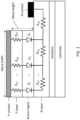
- FIG. 1 A general light-emitting diode (LED) is illustrated in FIG. 1 , including a light-emitting structure having an n-layer, a p-layer and an active-region inserted in-between the n-layer and p-layer.
- An n-layer is a layer doped with n-type dopant.
- a p-layer is a layer doped with p-type dopant.
- the light-emitting structure can be formed on a substrate or a template, and an n-contact and a p-contact are formed on the n-layer and p-layer, respectively.
- n-contact In order to form the n-contact to the n-layer, a standard LED lithography and etch process is employed to remove parts of the p-layer and active-region so that a light-emitting mesa is formed and part of the n-layer is exposed for the n-contact formation.
- the p-contact and n-contact are made of proper metal layers and form ohmic contacts to the p-layer and n-layer, respectively. As shown in FIG. 1 , the p-contact covers the whole light-emitting mesa area, so that the top portion of the p-layer is made equipotential by the p-contact. Holes therefore can be uniformly and vertically injected into the active-region from the p-layer.
- the n-contact is only formed on a part of the n-layer. Electrons injected by the n-contact therefore need to move transversely or laterally in order to flow into the active-region. During operation, a positive voltage is exerted to the p-contact relative to the n-contact, so that holes and electrons are respectively injected into the active-region from the p- and n-layers, to recombine to emit light.
- FIG. 1 Also shown in FIG. 1 is an equivalent circuit of the LED, including many diodes (D 1 , D 2 , ..., D i ), resistances in the n-layer (R n1 , R n2 , ..., R ni ), and resistances in the p-layer (R p1 , R p2 , ..., R pi ).
- D 1 , D 2 , ..., D i many diodes
- R n1 , R n2 resistances in the n-layer
- R ni resistances in the n-layer
- R p1 , R p2 resistances in the p-layer
- R pi resistances in the p-layer
- the mesa shown in FIG. 1 can be of a width tens up to a few hundred microns, and height only a few hundred nanometers.
- UV LEDs with optical emission wavelengths less than 360 nm are made of group-III nitride compound semiconductors such as AlGaN alloys.
- a typical UV LED includes a UV transparent substrate (e.g.: sapphire) and an AlN layer formed on the substrate. This AlN layer serves as an epitaxial template to support a UV light-emitting structure, which typically includes an n-type AlGaN structure, a p-type AlGaN structure, and a light-emitting region or active-region commonly made of AlGaN multiple-quantum-well (MQW) sandwiched in-between the n-type and p-type AlGaN structures.
- MQW multiple-quantum-well
- An AlGaN structure can be made of an AlGaN layer or many AlGaN layers joint forces to deliver a better function, such as to improve material quality, conductivity and/or carrier confinement.
- the Al-contents in the AlGaN layers/structures determine the optical emission wavelength of the UV LEDs.
- the optical emissions of wavelength less than 280 nm possess strong germicidal effect, making them ideal for food, water, air and surface disinfections.
- UV C-band (UVC) LEDs of emissions in the range of 200-280 nm the Al-content (x) of the n-type Al x Ga 1-x N structure needs to be in the range of 0.55-1 (i.e., x ⁇ [55%-100%]).
- the donor activation energies in such Al x Ga 1- x N layers increase quickly with x, making the dopant activation efficiency hence the conductivity drops exponentially with the Al-content (see, e.g., M. L. Nakarmi et al, Appl. Phys. Lett. 85, 3769 (2004 )). Because of this limited conductivity of the n-type AlGaN structures, UVC LEDs usually suffer severer current crowding effect as compared to GaN-based visible LEDs.
- An apparatus has a current spreading base with an n-contact.
- the current spreading base has a small n-type resistivity to promote lateral electron flow.
- a current spreading cap is on top of the current spreading base.
- the current spreading cap has a large n-type resistivity to suppress vertical electron flow and promote lateral electron flow.
- An active region is on top of the current spreading cap.
- a p-type structure is on top of the active region with a p-contact.
- Sheet resistance R n ⁇ of the current spreading base is experimentally established, the half width x F of a mesa is selected and the current spreading cap thickness h c is selected to collectively promote uniform current injection into the active region.
- group III nitride in general refers to metal nitride with cations selecting from group IIIA of the periodic table of elements. That is to say, III-nitride includes BN, AlN, GaN, InN and their ternary (e.g., AlGaN, InGaN, InAlN, et al) and quaternary (e.g., AlInGaN, BAlGaN, et al) alloys.
- a quaternary can be reduced to a ternary for simplicity if one of the group III elements is significantly small so that its existence does not affect the intended function of a layer made of such material.
- a ternary AlInGaN For example, if the In-composition in a quaternary AlInGaN is significantly small, smaller than 1%, then this AlInGaN quaternary can be shown as ternary AlGaN for simplicity.
- a ternary can be reduced to a binary for simplicity if one of the group III elements is significantly small. For example, if the In-composition in a ternary InGaN is significantly small, smaller than 1%, then this InGaN ternary can be shown as binary GaN for simplicity.
- Group III nitride may also include a small amount of transition metal nitride such as TiN, ZrN, HfN with molar fraction not larger than 10%.
- III-nitride or nitride may include Al x In y Ga z Ti( 1-x-y-z) N, Al x In y Ga z Zr (1-x-y-z) N, Al x In y Ga z Hf (1-x-y-z) N, with (1-x-y-z) ⁇ 10%.
- the bandgap of a group III nitride is determined by its composition. For examples, the bandgaps of InN, GaN, and AlN at room-temperature are 0.7, 3.4, and 6.2 eV, respectively.
- the bandgap of an AlGaN alloy increases with its Al-composition (or, Al-content).
- blue, green and UV light-emitting devices such as light-emitting diodes (LEDs) commonly adopt a laminate light-emitting structure containing a quantum well active region, an n-type group III nitride structure on one side of the active-region for injecting electrons into the active region, and a p-type group III nitride structure on the other side of the active region for injecting holes into the active region.
- This light-emitting structure is generally formed over a substrate, which can be selected from silicon (Si), silicon carbide (SiC), AlN and sapphire.
- Si silicon
- SiC silicon carbide
- AlN aluminumN
- sapphire usually c-plane sapphire is the number one choice of selection for visible and UV LEDs.
- a c-plane sapphire substrate has a (0002) plane to receive epitaxial growth layers.
- An LED also includes at least a metal p-contact and at least a metal n-contact formed on the p-type and n-type structures, respectively.
- the n-contacts optionally are only formed on a portion of the n-type layers, as a result, electrons injected from the n-contacts need to transport laterally in the n-type layers so that uniform electron injection into the active region can be realized.
- One aspect of the present invention provides an n-type structure which is a current spreading structure for an LED.
- the current spreading structure includes a current spreading base and a current spreading cap, wherein the current spreading base optionally include a high bandgap ( E g ) layer and a low bandgap layer, and the n-contacts are formed on the low bandgap layer of the current spreading base, and the bandgap of the current spreading cap is higher than that of the low bandgap layer of the current spreading base, the resistivity of the current spreading cap is at least 1000 times that of the current spreading base.
- E g high bandgap
- n-contacts are formed on the low bandgap layer of the current spreading base
- the bandgap of the current spreading cap is higher than that of the low bandgap layer of the current spreading base
- the resistivity of the current spreading cap is at least 1000 times that of the current spreading base.
- FIG. 2A A laminate or layered structure of a LED according to one aspect of the present disclosure is given in FIG. 2A .
- the LED structure is formed on substrate 10, which can be selected from Si, SiC, AlN and sapphire.
- a template 20 is then formed on substrate 10.
- Template 20 can be made of AlN or undoped GaN.
- template 20 is an AlN layer.
- a current spreading structure 30, which is generally an n-type structure and includes a current spreading base 33 and a current spreading cap 36.
- Base 33 optionally has good n-type conductivity, i.e., being of small n-type resistivity, so that electrons can have sufficient lateral flow capability.
- Cap 36 optionally has much higher n-type resistivity, so that it can suppress electrons' vertical flow and enforce their lateral flow.
- Base 33 and cap 36 can be respectively made of one layer or many layers in order to implement their respective functionalities.
- active-region 40 Formed over current spreading structure 30 is active-region 40, and formed on active-region 40 is p-type structure 50.
- n-type layer 38 In-between active-region 40 and current spreading structure 30 there is an n-type layer 38, which is optionally doped with Si to a high concentration, e.g, 8.0 ⁇ 10 18 -2.0 ⁇ 10 19 cm -3 , to provide good screening effect for the electric field within the active-region 40.
- P-contact 70 and n-contact 80 are formed on p-type structure 50 and current spreading base 33, respectively.
- P-contact 70 (n-contact 80) may include a p-ohmic (n-ohmic) contact layer and a thick metal probe layer.
- light-emitting mesa 1 has to be formed via etching part of the p-type structure 50, active-region 40, n-type layer 38, and cap 36 to expose part of base 33 on which n-contact 80 can be formed.
- FIG. 2B A plan view of the LED having the laminate structure shown in FIG. 2A is given in FIG. 2B . As seen, the light-emitting area of the LED is made of many (5 shown in FIG.
- FIGs. 2A and 2B finger-type light-emitting mesas 1 (covered by p-contacts 70), each of a half width x F (i.e., finger mesa width 2 x F ).
- the LED embodiments shown in FIGs. 2A and 2B can be called lateral LEDs, as electrons injected from n-contact 80 need to move laterally along current spreading base 33 so that they can be injected more uniformly into active-region 40 defined by mesas 1.
- FIG. 3 Another LED embodiment which can be called a vertical LED according to this disclosure is illustrated in FIG. 3 .
- substrate 10 is removed, and the exposed surface of template 20 is roughened for better light extraction, and n-contacts 80 are formed into the current spreading base 33. Electrons injected from n-contacts 80 have a great portion that can be injected vertically into the active-region 40. Still, there are regions in active-region 40 that need electrons to be injected laterally. These regions are of width 2 x F , as shown in FIG. 3 , being out of the vertical projections of n-contacts 80.
- Another aspect of the present invention is to design the current spreading structure 30 so that electrons injected from the n-contacts 80 can flow uniformly into the active-region 40 beneath the p-contacts 70. This requires current spreading structure 30 to be of wellbalanced lateral conduction to its vertical conduction.
- ⁇ 1 qn ⁇
- q, n, and ⁇ are electron's elementary charge, carrier concentration, and carrier mobility, respectively.
- Cap 36 is of thickness h c and resistivity ⁇ c
- base 33 is of thickness h n and resistivity ⁇ n .
- the light-emitting mesa is defined with a length a and half width x F (e.g., seen in FIGs. 2A and 2B ). After electrons being injected from n-contact 80, they will first flow laterally in the base 33 towards mesa 1. Once reaching mesa 1, the electrons will sense the resistance variations in all directions, namely, in the lateral and vertical directions.
- the desired ⁇ V F is limited to less than 0.5 V, or less than 0.3 V, or less than 0.2 V.
- FIG. 5A is a plot of the required minimal resistivity of the current spreading cap 36 for uniform electron injection into the active-region 40 defined by mesa 1, as a function of the sheet resistance of the current spreading base 33 for three different mesa half widths (50, 100, and 150 ⁇ m).
- the thickness of the current spreading cap is fixed to be 0.2 ⁇ m.
- the wider the mesa half width is, the larger the minimal resistivity of the current spreading cap.
- the larger the sheet resistance of the current spreading base 33 the higher the minimal resistivity of the current spreading cap 36.
- FIG. 5B plots the required minimal resistivity of the current spreading cap for uniform electron injection into the active-region 40 defined by mesa 1, as a function of the light-emitting mesa (e.g., mesa 1 in FIGs. 2A and 2B ) finger half width for current spreading bases of three sheet resistances (8, 80, and 800 ⁇ ).
- the thickness of the current spreading cap is fixed to be 0.2 ⁇ m.
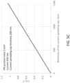
- FIG. 5C plots the forward voltage increase ( ⁇ V F ) of a disclosed LED as function of the resistivity of the current spreading cap.
- the LED p-n junction area, forward current, and current spreading cap thickness are fixed to be 1.0 mm 2 , 350 mA, and 0.2 ⁇ m, respectively.
- ⁇ V F increases linearly with ⁇ c , the resistivity of the current spreading cap.
- the desired ⁇ V F is limited to less than 0.5 V, or less than 0.3 V, or less than 0.2 V, therefore the required minimal resistivity of the current spreading cap is less than ⁇ 715, 430, and 290 ⁇ cm , respectively.
- GaN and AlGaN layers of these resistivities are not easy to obtain.
- Another aspect of the present disclosure is to provide methods to form GaN and AlGaN layers as current spreading caps of resistivity of a few tens to thousands ⁇ cm.
- current spreading cap 36 can be unintentionally doped, lightly Si-doped (e.g., doping level in the 10 15 -10 17 cm -3 range), or intentionally doped with deep level impurities such as carbon (C) and/or iron (Fe) (doping level 10 17 -10 19 cm -3 range) to increase the resistivity.
- current spreading cap 36 can include at least an AlGaN layer of high Al-content, with Al-content being 70% or above, for example, being 70%-100%, or 75%-95%.
- the resistivity of current spreading cap 36 can be accessed via Van der Pauw Hall effect measurement, which is a technique commonly used to measure the resistivity and the Hall coefficient of an approximately two-dimensional sample (i.e., the sample thickness much less than its lateral dimensions) in the semiconductor field of interest.
- current spreading cap 36 is made of a high-Al-content AlGaN layer, whose mobility are known to be in the range of 30-60 cm 2 /(v.s), for example, 50 cm 2 /(v.s), then, a carrier concentration in the range of 1.0 ⁇ 10 14 -1.0 ⁇ 10 16 cm -3 will indicate a resistivity 12.5-1250 ⁇ cm .
- the carrier concentration can be measured via capacitance-voltage (C-V) profiling, which is a well-known technique for characterizing semiconductor materials and devices.
- C-V capacitance-voltage
- FIG. 6A Illustrated in FIG. 6A is a laminate structure of a current spreading structure 30 made of Al x Ga 1-x N according to one aspect of the present disclosure, with an illustrative Al-content profile given in FIG. 6B , which can also be viewed as an illustrative bandgap ( E g ( x )) profile of the Al x Ga 1-x N current spreading structure 30.
- the current spreading base 33 includes three layers, i.e., layer 331, layer 332 and layer 333.
- Layer 331 can be formed on template 20 so its Al-content is close to that of the template 20. If template 20 is made of AlN, the Al-content of layer 331 can be close to AlN, i.e., in the range of 70-100%, or 80-95%.
- Layer 331 can be Si-doped.
- Layer 332 is the main block for current spreading base 33, can be of less Al-content (hence E g ) as compared to layer 331.
- the Al-content of layer 332 can optionally be in the range of 58-65%.
- Layer 332 is of thickness in the range of 1.0-3.0 ⁇ m, and doped with Si of concentration 5-15 ⁇ 10 18 cm -3 to provide good conductance.
- Formed on layer 332 is layer 333, serving as n-type contact layer to receive n-contact 80.
- layer 333 is of the lowest Al-content (hence E g ) as compared to layers 331, 332, and is heavily doped with Si, with concentration in the range of 6-25 ⁇ 10 18 cm -3 .
- Layer 333 optionally is of thickness 100-500 nm, or 150-400 nm.
- Current spreading cap 36 has a resistivity ⁇ c optionally satisfying inequality (1). Or, as a rule of thumb, according to one aspect of the present invention, the resistivity of the current spreading cap 36 is at least 1000 times of that of the current spreading base 33.
- Cap 36 can be of the same Al-content as that of layer 332, or have Al-content (hence E g ) higher than that of layer 332.
- the Al-content of layer 333 can be 52-58% (e.g., 55%), and Al-content of current spreading cap 36 is 70-85% (e.g., 76%).
- the Al-content difference, ⁇ x, between cap 36 and layer 333 is at least 10%, or 15%, or 20%, or 25%.
- the Al-content of cap 36 being higher than that of layer 333 can generate interface positive charges due to polarization discontinuity, adding an additional mechanism to cause electrons to spread laterally to form a two-dimensional electron gas within layer 333 in the vicinity of the layer 333/cap 36 interface.
- FIG. 7A Illustrated in FIG. 7A is a laminate structure of another current spreading structure 30 made of Al x Ga 1-x N according to one aspect of the present disclosure, with an illustrative Al-content profile given in FIG. 7B .
- the current spreading cap 36 includes multiple layers, i.e., include a periodic laminate structure made of alternatively stacking layers 361 and 362 for multiple times, e.g., for 3-5, or more times. Layer 361 may have higher Al-content than layer 362. This arrangement makes electrons in current spreading cap 36 have additional lateral spreading capability.
- layers 361 and 362 can have respective Al-content of 80% and 65%.
- Cap 36 can be made of layer 361 and layer 362 without being a periodic laminate structure.
- the Al-content difference, ⁇ x, between layer 361 and layer 333 is at least 10%, or 15%, or 20%, or 25%.
- Embodiments of UVC LEDs with current spreading structures 30 are described using a semiconductor layer formation technology called metalorganic chemical vapor deposition (MOCVD).
- MOCVD metalorganic chemical vapor deposition
- TMA trimethylaluminum
- TMG trimethylgallium
- ammonia aluminum
- Al gallium
- N nitrogen
- FIG. 2A Illustrated in FIG. 2A is a cross-sectional schematic view of a UV LED structure formed over a substrate 10 according to an embodiment of the present invention.
- Substrate 10 can be made from c-plane sapphire.
- AlN template 20 Formed over substrate 10 is an AlN template 20, which can be made of a thick AlN layer, for example, with a thickness of 1.5-6.0 ⁇ m to fully coalesce on the substrate 10.
- Formed over template 20 is a thick n-AlGaN current spreading structure 30 for electron supply and n-type ohmic contact formation.
- Structure 30 may include a current spreading base 33 and a current spreading cap 36.
- a thin (0.2-0.5 ⁇ m such as 0.4 ⁇ m, n 2.0 ⁇ 10 18 -6.0 ⁇ 10 18 cm -3 ) n-type N-AlGaN layer 331, a thick (1.0-5.0 ⁇ m such as 1.3 ⁇ m,
- the Al-contents of the layers 331, 332 and 333 are respectively 73%, 64% and 55%.
- Formed on the current spreading base 33 is a ⁇ 0.15 ⁇ m current spreading cap 36, which is unintentionally doped and of Al-content -70%.
- Formed on cap 36 is layer 38, an Al0.7Ga0.3N of ⁇ 10 nm-thick and doped with Si at 1.5 ⁇ 10 19 cm -3 for MQW active-region polarization field screening.
- active-region 40 made of Al b Ga 1-b N/Al w Ga 1-w N multiple-quantum-well (MQW).
- Active-region 40 is made of alternatingly stacked n-Al b Ga 1-b N barrier and Al w Ga 1-w N well for a few times, for example, for 3-8 times.
- the barrier thickness is in the range of 8 - 16 nm, and the well thickness is 1.2 - 5.0 nm.
- the total thickness of active region 40 is usually less than 200 nm, for example, being 75 nm, 100 nm, or 150 nm.
- the n-Al b Ga 1-b N barrier and Al w Ga 1-w N well may have an Al-composition in the range of 0.3-1.0, and 0.0 - 0.85, respectively, and the Al-composition difference of the barrier and well is at least 0.15, or so to ensure a barrier-well bandgap difference ( ⁇ E g ) of at least 400 meV to secure quantum confinement effect.
- active-region 40 is a p-type AlGaN structure 50.
- Structure 50 can be a p-AlGaN layer of uniform or varying Al-composition, or a p-AlGaN superlattice structure, or a p-AlGaN MQW structure, or a p-AlGaN multilayer structure serving as hole injecting and electron blocking layer. Structure 50 has enough Al-composition and modulation to allow for sufficient electron blocking and hole injection efficiencies. Further, structure 50 is also efficient in spreading hole current laterally. Structure 50 may also contain a p-contact layer to receive p-contact 70.
- the p-contact layer can be a thin (0.6 -2.0 nm), strained, and heavily acceptor-doped nitride layer (e.g., Mg-doped, or Mg and Si co-doped to a concentration about 10 19 -10 20 cm -3 or more).
- the p-contact layer prefers to be a Mg-doped AlGaN layer with Al-composition larger than 0.4, or with Al-composition to be from 0.45 to 1.0.
- P-contact 70 forms p-ohmic contact to p-type structure 50, and optionally is a p-ohmic contact and reflector as well.
- P-contact 70 may include a rhodium layer, or a palladium layer, optionally, also include a 2-8 ⁇ m gold layer or gold tin layer.
- n-contact 80 is also formed on current spreading base 33 .
- n-contact 80 can be made of thin metal layer stacks such as titanium/aluminum/titanium/gold (Ti/Al/Ti/Au) with respective layer thickness of 30-40/70-80/10-20/80-100 nm, for example 35/75/15/90 nm, or V/Al/V/Ag, V/Al/V/Au, and V/Al/Ti/Au, of respective thicknesses such as 20/60/20/100 nm.
- n-contact 80 is preferred to be formed on the heavily n-type doped N + -AlGaN layer 333.
- N-contact 80 may also include a thick (2-10 ⁇ m) gold or gold tin layer.
- FIGs. 8 and 9 Plotted in FIGs. 8 and 9 are the Al-content profiles for a 275 nm and a 268 nm UVC LED embodiments of the present invention.
- the 275 nm LED utilizes a current spreading cap 36 made of a single Al 0.7 Ga 0.3 N layer, while the 268 nm LED has a current spreading cap 36 made of multiple AlGaN layers including a layer 362, and a laminate structure made of periodically stacking of layer 361/362 four times.
- the Al-content profiles in FIGs. 8 and 9 were measured by energy dispersive X-ray spectroscopy in a cross-sectional transmission electron microscopy system.
- the present invention has mostly used UVC LEDs as exemplary embodiments.
- the scope of the present invention is not limited to the disclosed embodiments.
- it is intended to cover various modifications and similar arrangement or equivalents which can be obtained by a person skilled in the art without creative work or undue experimentation.
Abstract
An apparatus has a current spreading base with an n-contact. The current spreading base has a small n-type resistivity to promote lateral electron flow. A current spreading cap is on top of the current spreading base. The current spreading cap has a large n-type resistivity to suppress vertical electron flow and promote lateral electron flow. An active region is on top of the current spreading cap. A p-type structure is on top of the active region with a p-contact. Sheet resistance Rn  of the current spreading base is experimentally established, the half width xF of a mesa is selected and the current spreading cap thickness hc is selected to collectively promote uniform current injection into the active region.
Description
- This application claims priority to
U.S. Patent Application No. 17/936,802 filed September 29, 2022 - The present invention relates to light-emitting diodes. More particularly, the invention is directed to current spreading structures for group-III nitride light-emitting diodes.
- A general light-emitting diode (LED) is illustrated in
FIG. 1 , including a light-emitting structure having an n-layer, a p-layer and an active-region inserted in-between the n-layer and p-layer. An n-layer is a layer doped with n-type dopant. Similarly, a p-layer is a layer doped with p-type dopant. The light-emitting structure can be formed on a substrate or a template, and an n-contact and a p-contact are formed on the n-layer and p-layer, respectively. In order to form the n-contact to the n-layer, a standard LED lithography and etch process is employed to remove parts of the p-layer and active-region so that a light-emitting mesa is formed and part of the n-layer is exposed for the n-contact formation. The p-contact and n-contact are made of proper metal layers and form ohmic contacts to the p-layer and n-layer, respectively. As shown inFIG. 1 , the p-contact covers the whole light-emitting mesa area, so that the top portion of the p-layer is made equipotential by the p-contact. Holes therefore can be uniformly and vertically injected into the active-region from the p-layer. However, the n-contact is only formed on a part of the n-layer. Electrons injected by the n-contact therefore need to move transversely or laterally in order to flow into the active-region. During operation, a positive voltage is exerted to the p-contact relative to the n-contact, so that holes and electrons are respectively injected into the active-region from the p- and n-layers, to recombine to emit light. - Also shown in
FIG. 1 is an equivalent circuit of the LED, including many diodes (D1, D2, ..., Di), resistances in the n-layer (Rn1, Rn2, ..., Rni), and resistances in the p-layer (Rp1, Rp2, ..., Rpi). Note that the illustration inFIG. 1 is not drawn to scale. The lateral dimension is actually much larger than the vertical dimension. In general, the mesa shown inFIG. 1 can be of a width tens up to a few hundred microns, and height only a few hundred nanometers. Therefore, the total lateral resistance (R ∥ = Σ k Rnk ) is much larger than the total vertical resistance (
- In the prior art, there are practices to mitigate the current crowding effect, basically via incorporation of a current spreading feature into the LEDs. Examples can be found in the US patent Nos.
US8,330,174 ,US9,705,033 US7,998,771 , andUS8,501,513 . The prior art practices are, however, purely empirical. There lacks a clear design rule of the current spreading features in the prior art, and it is difficult to predict the effectiveness of the prior art designs. - The current crowding effect is expected to be severer for ultraviolet (UV) LEDs. UV LEDs with optical emission wavelengths less than 360 nm are made of group-III nitride compound semiconductors such as AlGaN alloys. A typical UV LED includes a UV transparent substrate (e.g.: sapphire) and an AlN layer formed on the substrate. This AlN layer serves as an epitaxial template to support a UV light-emitting structure, which typically includes an n-type AlGaN structure, a p-type AlGaN structure, and a light-emitting region or active-region commonly made of AlGaN multiple-quantum-well (MQW) sandwiched in-between the n-type and p-type AlGaN structures. An AlGaN structure can be made of an AlGaN layer or many AlGaN layers joint forces to deliver a better function, such as to improve material quality, conductivity and/or carrier confinement. The Al-contents in the AlGaN layers/structures determine the optical emission wavelength of the UV LEDs. The optical emissions of wavelength less than 280 nm possess strong germicidal effect, making them ideal for food, water, air and surface disinfections.
- For UV C-band (UVC) LEDs of emissions in the range of 200-280 nm, the Al-content (x) of the n-type AlxGa 1-x N structure needs to be in the range of 0.55-1 (i.e., x ∈ [55%-100%]). The donor activation energies in such AlxGa 1- xN layers increase quickly with x, making the dopant activation efficiency hence the conductivity drops exponentially with the Al-content (see, e.g., M. L. Nakarmi et al, Appl. Phys. Lett. 85, 3769 (2004)). Because of this limited conductivity of the n-type AlGaN structures, UVC LEDs usually suffer severer current crowding effect as compared to GaN-based visible LEDs.
- Thus, there is a need for general design rules to mitigate LED current crowding effect for various UV LED embodiments with uniform current injections.
- An apparatus has a current spreading base with an n-contact. The current spreading base has a small n-type resistivity to promote lateral electron flow. A current spreading cap is on top of the current spreading base. The current spreading cap has a large n-type resistivity to suppress vertical electron flow and promote lateral electron flow. An active region is on top of the current spreading cap. A p-type structure is on top of the active region with a p-contact. Sheet resistance

- The accompanying drawings, which are included to provide a further understanding of the invention and constitute a part of this application, illustrate embodiments of the invention and together with the description serve to explain the principle of the invention. Like reference numbers in the figures refer to like elements throughout, and a layer can refer to a group of layers associated with the same function.
-
FIG. 1 illustrates a laminate structure of a prior art LED, together with an equivalent circuit. -
FIG. 2A illustrates a laminate structure of a lateral LED according to this disclosure, together with an equivalent circuit. -
FIG. 2B illustrates a plan view of a lateral LED with a laminate structure given inFIG. 2A . -
FIG. 3 illustrates a laminate structure of a vertical LED according to this disclosure. -
FIG. 4 illustrate a current spreading structure according to this disclosure, including a current spreading base and a current spreading cap. -
FIG. 5A plots the required minimal resistivity of the current spreading cap as a function of the sheet resistance of the current spreading base for three different mesa half widths. -
FIG. 5B plots the required minimal resistivity of the current spreading cap as function of the finger mesa half width for three different current spreading base sheet resistances. -
FIG. 5C plots the forward voltage increase of an embodiment LED as function of the resistivity of the current spreading cap. -
FIG. 6A illustrates a laminate structure of a current spreading structure according to one aspect of the present disclosure. -
FIG. 6B illustrates the Al-content of the current spreading structure given inFIG. 6A . -
FIG. 7A illustrates a laminate structure of a current spreading structure according to one aspect of the present disclosure. -
FIG. 7B illustrates the Al-content of the current spreading structure given inFIG. 7A . -
FIG. 8 is a plot of a part of the Al-composition profile of a UV LED according to one aspect of the present disclosure. -
FIG. 9 is a plot of a part of the Al-composition profile of a UV LED according to one aspect of the present disclosure. - Throughout the specification, the term group III nitride in general refers to metal nitride with cations selecting from group IIIA of the periodic table of elements. That is to say, III-nitride includes BN, AlN, GaN, InN and their ternary (e.g., AlGaN, InGaN, InAlN, et al) and quaternary (e.g., AlInGaN, BAlGaN, et al) alloys. In this specification, a quaternary can be reduced to a ternary for simplicity if one of the group III elements is significantly small so that its existence does not affect the intended function of a layer made of such material. For example, if the In-composition in a quaternary AlInGaN is significantly small, smaller than 1%, then this AlInGaN quaternary can be shown as ternary AlGaN for simplicity. Using the same logic, a ternary can be reduced to a binary for simplicity if one of the group III elements is significantly small. For example, if the In-composition in a ternary InGaN is significantly small, smaller than 1%, then this InGaN ternary can be shown as binary GaN for simplicity. Group III nitride may also include a small amount of transition metal nitride such as TiN, ZrN, HfN with molar fraction not larger than 10%. For example, III-nitride or nitride may include AlxInyGazTi(1-x-y-z)N, AlxInyGazZr(1-x-y-z)N, AlxInyGazHf(1-x-y-z)N, with (1-x-y-z)≤10%. The bandgap of a group III nitride is determined by its composition. For examples, the bandgaps of InN, GaN, and AlN at room-temperature are 0.7, 3.4, and 6.2 eV, respectively. The bandgap of an AlGaN alloy increases with its Al-composition (or, Al-content).
- As well known, blue, green and UV light-emitting devices such as light-emitting diodes (LEDs) commonly adopt a laminate light-emitting structure containing a quantum well active region, an n-type group III nitride structure on one side of the active-region for injecting electrons into the active region, and a p-type group III nitride structure on the other side of the active region for injecting holes into the active region. This light-emitting structure is generally formed over a substrate, which can be selected from silicon (Si), silicon carbide (SiC), AlN and sapphire. In consideration of cost, commercial viability and UV transparency, sapphire, usually c-plane sapphire is the number one choice of selection for visible and UV LEDs. A c-plane sapphire substrate has a (0002) plane to receive epitaxial growth layers.
- An LED also includes at least a metal p-contact and at least a metal n-contact formed on the p-type and n-type structures, respectively. For the sake of light extraction, the n-contacts optionally are only formed on a portion of the n-type layers, as a result, electrons injected from the n-contacts need to transport laterally in the n-type layers so that uniform electron injection into the active region can be realized. One aspect of the present invention provides an n-type structure which is a current spreading structure for an LED. The current spreading structure includes a current spreading base and a current spreading cap, wherein the current spreading base optionally include a high bandgap (Eg ) layer and a low bandgap layer, and the n-contacts are formed on the low bandgap layer of the current spreading base, and the bandgap of the current spreading cap is higher than that of the low bandgap layer of the current spreading base, the resistivity of the current spreading cap is at least 1000 times that of the current spreading base.
- A laminate or layered structure of a LED according to one aspect of the present disclosure is given in
FIG. 2A . The LED structure is formed onsubstrate 10, which can be selected from Si, SiC, AlN and sapphire. Atemplate 20 is then formed onsubstrate 10.Template 20 can be made of AlN or undoped GaN. For UV LEDs, optionally,template 20 is an AlN layer. Formed overtemplate 20 is a current spreadingstructure 30, which is generally an n-type structure and includes a current spreadingbase 33 and a current spreadingcap 36.Base 33 optionally has good n-type conductivity, i.e., being of small n-type resistivity, so that electrons can have sufficient lateral flow capability.Cap 36 optionally has much higher n-type resistivity, so that it can suppress electrons' vertical flow and enforce their lateral flow.Base 33 andcap 36 can be respectively made of one layer or many layers in order to implement their respective functionalities. - Formed over current spreading
structure 30 is active-region 40, and formed on active-region 40 is p-type structure 50. Optionally, in-between active-region 40 and current spreadingstructure 30 there is an n-type layer 38, which is optionally doped with Si to a high concentration, e.g, 8.0×10¹⁸-2.0×1019 cm-3, to provide good screening effect for the electric field within the active-region 40. - Finally, p-
contact 70 and n-contact 80 are formed on p-type structure 50 and current spreadingbase 33, respectively. P-contact 70 (n-contact 80) may include a p-ohmic (n-ohmic) contact layer and a thick metal probe layer. In order to accessbase 33, light-emittingmesa 1 has to be formed via etching part of the p-type structure 50, active-region 40, n-type layer 38, and cap 36 to expose part ofbase 33 on which n-contact 80 can be formed. A plan view of the LED having the laminate structure shown inFIG. 2A is given inFIG. 2B . As seen, the light-emitting area of the LED is made of many (5 shown inFIG. 2B ) finger-type light-emitting mesas 1 (covered by p-contacts 70), each of a half width xF (i.e., finger mesa width 2xF ). The LED embodiments shown inFIGs. 2A and2B can be called lateral LEDs, as electrons injected from n-contact 80 need to move laterally along current spreadingbase 33 so that they can be injected more uniformly into active-region 40 defined bymesas 1. - Another LED embodiment which can be called a vertical LED according to this disclosure is illustrated in
FIG. 3 . In comparison to the LED embodiment given inFIG. 2A , in this vertical LED embodiment,substrate 10 is removed, and the exposed surface oftemplate 20 is roughened for better light extraction, and n-contacts 80 are formed into the current spreadingbase 33. Electrons injected from n-contacts 80 have a great portion that can be injected vertically into the active-region 40. Still, there are regions in active-region 40 that need electrons to be injected laterally. These regions are of width 2xF , as shown inFIG. 3 , being out of the vertical projections of n-contacts 80. - Another aspect of the present invention is to design the current spreading
structure 30 so that electrons injected from the n-contacts 80 can flow uniformly into the active-region 40 beneath the p-contacts 70. This requires current spreadingstructure 30 to be of wellbalanced lateral conduction to its vertical conduction. - The resistivity (ρ) of a semiconductor layer can be calculated as


- Consider the electrical current generated by electron flows in the
base 33 andcap 36. In order to have a better understanding, the current spreadingstructure 30 is illustrated in an exploded view inFIG. 4 , where the electron flows are indicated by arrows.Cap 36 is of thickness hc and resistivity ρc, andbase 33 is of thickness hn and resistivity ρn. Suppose the light-emitting mesa is defined with a length a and half width xF (e.g., seen inFIGs. 2A and2B ). After electrons being injected from n-contact 80, they will first flow laterally in the base 33 towardsmesa 1. Once reachingmesa 1, the electrons will sense the resistance variations in all directions, namely, in the lateral and vertical directions. On their way transversely to the left (x increases), they sense the changes of the lateral and vertical resistances to be


region 40. If
active region 40 defined by the light-emittingmesa 1. This requires an inequality (1) to hold:

base 33. Inequality (1) tells, that in order to have uniform electron injection into theactive region 40 defined by the light-emittingmesa 1, the required minimal resistivity of the current spreadingcap 36 needs to be proportional to


- The addition of the
cap 36 can result in a forward voltage increase (ΔVF ), which depends on the p-n junction area (A) and forward current (I), which is given by equation (2):
- In practice, the desired ΔVF is limited to less than 0.5 V, or less than 0.3 V, or less than 0.2 V.
-
FIG. 5A is a plot of the required minimal resistivity of the current spreadingcap 36 for uniform electron injection into the active-region 40 defined bymesa 1, as a function of the sheet resistance of the current spreadingbase 33 for three different mesa half widths (50, 100, and 150 µm). The thickness of the current spreading cap is fixed to be 0.2 µm. For the same sheet resistance of the current spreadingbases 33, the wider the mesa half width is, the larger the minimal resistivity of the current spreading cap. Also, the larger the sheet resistance of the current spreadingbase 33, the higher the minimal resistivity of the current spreadingcap 36. For example, if

-
FIG. 5B plots the required minimal resistivity of the current spreading cap for uniform electron injection into the active-region 40 defined bymesa 1, as a function of the light-emitting mesa (e.g.,mesa 1 inFIGs. 2A and2B ) finger half width for current spreading bases of three sheet resistances (8, 80, and 800 Ω). Here the thickness of the current spreading cap is fixed to be 0.2 µm. In order to make electrons spread into larger lateral distances to have larger mesa half width xF, we need to have higher resistivity for the current spreadingcap 36. For example, if


-
FIG. 5C plots the forward voltage increase (ΔVF ) of a disclosed LED as function of the resistivity of the current spreading cap. Here the LED p-n junction area, forward current, and current spreading cap thickness are fixed to be 1.0 mm2, 350 mA, and 0.2 µm, respectively. ΔVF increases linearly with ρc, the resistivity of the current spreading cap. In practice, the desired ΔVF is limited to less than 0.5 V, or less than 0.3 V, or less than 0.2 V, therefore the required minimal resistivity of the current spreading cap is less than ~715, 430, and 290 Ωcm, respectively. These numbers translate that, if

- GaN and AlGaN layers of these resistivities (i.e., a few tens to thousands Ωcm) are not easy to obtain. Another aspect of the present disclosure is to provide methods to form GaN and AlGaN layers as current spreading caps of resistivity of a few tens to thousands Ωcm.
- According to one embodiment, depending on the minimal resistivity demanded by inequality (1), current spreading
cap 36 can be unintentionally doped, lightly Si-doped (e.g., doping level in the 1015-1017 cm-3 range), or intentionally doped with deep level impurities such as carbon (C) and/or iron (Fe) (doping level 1017-1019 cm-3 range) to increase the resistivity. According to another embodiment, current spreadingcap 36 can include at least an AlGaN layer of high Al-content, with Al-content being 70% or above, for example, being 70%-100%, or 75%-95%. This is to ensure that the dopant activation energy in current spreadingcap 36 is deep that the resistivity can be controlled via intentionally n-type doping, such as Si-doping. The resistivity of current spreadingcap 36 can be accessed via Van der Pauw Hall effect measurement, which is a technique commonly used to measure the resistivity and the Hall coefficient of an approximately two-dimensional sample (i.e., the sample thickness much less than its lateral dimensions) in the semiconductor field of interest. If current spreadingcap 36 is made of a high-Al-content AlGaN layer, whose mobility are known to be in the range of 30-60 cm2/(v.s), for example, 50 cm2/(v.s), then, a carrier concentration in the range of 1.0×10¹⁴-1.0×1016 cm-3 will indicate a resistivity 12.5-1250 Ωcm. Here the carrier concentration can be measured via capacitance-voltage (C-V) profiling, which is a well-known technique for characterizing semiconductor materials and devices. - Illustrated in
FIG. 6A is a laminate structure of a current spreadingstructure 30 made of AlxGa1-xN according to one aspect of the present disclosure, with an illustrative Al-content profile given inFIG. 6B , which can also be viewed as an illustrative bandgap (Eg (x)) profile of the AlxGa1-xNcurrent spreading structure 30. The current spreadingbase 33 includes three layers, i.e.,layer 331,layer 332 andlayer 333.Layer 331 can be formed ontemplate 20 so its Al-content is close to that of thetemplate 20. Iftemplate 20 is made of AlN, the Al-content oflayer 331 can be close to AlN, i.e., in the range of 70-100%, or 80-95%.Layer 331 can be Si-doped.Layer 332 is the main block for current spreadingbase 33, can be of less Al-content (hence Eg ) as compared tolayer 331. For UVC LEDs, the Al-content oflayer 332 can optionally be in the range of 58-65%.Layer 332 is of thickness in the range of 1.0-3.0 µm, and doped with Si of concentration 5-15×1018 cm-3 to provide good conductance. Formed onlayer 332 islayer 333, serving as n-type contact layer to receive n-contact 80. In order to form good ohmic contact to n-contact 80,layer 333 is of the lowest Al-content (hence Eg ) as compared tolayers Layer 333 optionally is of thickness 100-500 nm, or 150-400 nm. Current spreadingcap 36 has a resistivity ρc optionally satisfying inequality (1). Or, as a rule of thumb, according to one aspect of the present invention, the resistivity of the current spreadingcap 36 is at least 1000 times of that of the current spreadingbase 33.Cap 36 can be of the same Al-content as that oflayer 332, or have Al-content (hence Eg ) higher than that oflayer 332. In some UVC LED embodiments, the Al-content oflayer 333 can be 52-58% (e.g., 55%), and Al-content of current spreadingcap 36 is 70-85% (e.g., 76%). The Al-content difference, Δx, betweencap 36 andlayer 333 is at least 10%, or 15%, or 20%, or 25%. The Al-content ofcap 36 being higher than that oflayer 333 can generate interface positive charges due to polarization discontinuity, adding an additional mechanism to cause electrons to spread laterally to form a two-dimensional electron gas withinlayer 333 in the vicinity of thelayer 333/cap 36 interface. - Illustrated in
FIG. 7A is a laminate structure of another current spreadingstructure 30 made of AlxGa1-xN according to one aspect of the present disclosure, with an illustrative Al-content profile given inFIG. 7B . As seen, the current spreadingcap 36 includes multiple layers, i.e., include a periodic laminate structure made of alternatively stackinglayers Layer 361 may have higher Al-content thanlayer 362. This arrangement makes electrons in current spreadingcap 36 have additional lateral spreading capability. For example, layers 361 and 362 can have respective Al-content of 80% and 65%. Therefore, the interface charges arising from polarization discontinuity and the band gap discontinuity betweenlayer 361 andlayer 362 will cause electrons to spread laterally.Cap 36 can be made oflayer 361 andlayer 362 without being a periodic laminate structure. The Al-content difference, Δx, betweenlayer 361 andlayer 333 is at least 10%, or 15%, or 20%, or 25%. - Embodiments of UVC LEDs with current spreading
structures 30 are described using a semiconductor layer formation technology called metalorganic chemical vapor deposition (MOCVD). For AlGaN MOCVD, usually trimethylaluminum (TMA), trimethylgallium (TMG) and ammonia are used as aluminum (Al), gallium (Ga) and nitrogen (N) sources, respectively. - Illustrated in
FIG. 2A is a cross-sectional schematic view of a UV LED structure formed over asubstrate 10 according to an embodiment of the present invention.Substrate 10 can be made from c-plane sapphire. Formed oversubstrate 10 is anAlN template 20, which can be made of a thick AlN layer, for example, with a thickness of 1.5-6.0 µm to fully coalesce on thesubstrate 10. Formed overtemplate 20 is a thick n-AlGaNcurrent spreading structure 30 for electron supply and n-type ohmic contact formation.Structure 30 may include a current spreadingbase 33 and a current spreadingcap 36. And the current spreadingbase 33 includes a thin (0.2-0.5 µm such as 0.4 µm, n=2.0 × 10¹⁸-6.0 × 1018 cm-3) n-type N-AlGaN layer 331, a thick (1.0-5.0 µm such as 1.3 µm, n=2.0 × 10¹⁸-9.0 × 1018 cm-3) n-type N-AlGaN layer 332 for current spreading, a heavily n-type doped (0.2-0.8 µm such as 0.40 µm, n=8 × 10¹⁸- 2 × 1019 cm-3) N+-AlGaN layer 333 for current spreading and to receive n-contact 80. The Al-contents of thelayers base 33 is a ~ 0.15 µm current spreadingcap 36, which is unintentionally doped and of Al-content -70%. Formed oncap 36 islayer 38, an Al0.7Ga0.3N of ~ 10 nm-thick and doped with Si at 1.5 × 1019 cm-3 for MQW active-region polarization field screening. Formed onlayer 38 is active-region 40, made of AlbGa1-bN/AlwGa1-wN multiple-quantum-well (MQW). Active-region 40 is made of alternatingly stacked n-AlbGa1-bN barrier and AlwGa1-wN well for a few times, for example, for 3-8 times. The barrier thickness is in the range of 8 - 16 nm, and the well thickness is 1.2 - 5.0 nm. The total thickness ofactive region 40 is usually less than 200 nm, for example, being 75 nm, 100 nm, or 150 nm. The n-AlbGa1-bN barrier and AlwGa1-wN well may have an Al-composition in the range of 0.3-1.0, and 0.0 - 0.85, respectively, and the Al-composition difference of the barrier and well is at least 0.15, or so to ensure a barrier-well bandgap difference (ΔEg ) of at least 400 meV to secure quantum confinement effect. Following active-region 40 is a p-type AlGaN structure 50.Structure 50 can be a p-AlGaN layer of uniform or varying Al-composition, or a p-AlGaN superlattice structure, or a p-AlGaN MQW structure, or a p-AlGaN multilayer structure serving as hole injecting and electron blocking layer.Structure 50 has enough Al-composition and modulation to allow for sufficient electron blocking and hole injection efficiencies. Further,structure 50 is also efficient in spreading hole current laterally.Structure 50 may also contain a p-contact layer to receive p-contact 70. Briefly, the p-contact layer can be a thin (0.6 -2.0 nm), strained, and heavily acceptor-doped nitride layer (e.g., Mg-doped, or Mg and Si co-doped to a concentration about 1019-1020 cm-3or more). For UVB/UVC LEDs (emissions from 200 nm - 315 nm), the p-contact layer prefers to be a Mg-doped AlGaN layer with Al-composition larger than 0.4, or with Al-composition to be from 0.45 to 1.0. P-contact 70 forms p-ohmic contact to p-type structure 50, and optionally is a p-ohmic contact and reflector as well. For example, P-contact 70 may include a rhodium layer, or a palladium layer, optionally, also include a 2-8 µ m gold layer or gold tin layer. - Also formed on current spreading
base 33 is an n-contact 80, which can be made of thin metal layer stacks such as titanium/aluminum/titanium/gold (Ti/Al/Ti/Au) with respective layer thickness of 30-40/70-80/10-20/80-100 nm, for example 35/75/15/90 nm, or V/Al/V/Ag, V/Al/V/Au, and V/Al/Ti/Au, of respective thicknesses such as 20/60/20/100 nm. As seen fromFIGs. 6B and7B , n-contact 80 is preferred to be formed on the heavily n-type doped N+-AlGaN layer 333. N-contact 80 may also include a thick (2-10 µ m) gold or gold tin layer. - Plotted in
FIGs. 8 and9 are the Al-content profiles for a 275 nm and a 268 nm UVC LED embodiments of the present invention. The 275 nm LED utilizes a current spreadingcap 36 made of a single Al0.7Ga0.3N layer, while the 268 nm LED has a current spreadingcap 36 made of multiple AlGaN layers including alayer 362, and a laminate structure made of periodically stacking oflayer 361/362 four times. The Al-content profiles inFIGs. 8 and9 were measured by energy dispersive X-ray spectroscopy in a cross-sectional transmission electron microscopy system. - The present invention has mostly used UVC LEDs as exemplary embodiments. However, it is to be understood that the scope of the present invention is not limited to the disclosed embodiments. On the contrary, it is intended to cover various modifications and similar arrangement or equivalents which can be obtained by a person skilled in the art without creative work or undue experimentation. The scope of the claims, therefore, should be accorded the broadest interpretation so as to encompass all such modifications and similar arrangements and equivalents.
Claims (16)
- An apparatus, comprising:a current spreading base with at least one n-contact, the current spreading base having a small n-type resistivity to promote lateral electron flow;a current spreading cap on top of the current spreading base, the current spreading cap with a large n-type resistivity to suppress vertical electron flow and promote lateral electron flow;a light-emitting active region on top of the current spreading cap; anda p-type structure on top of the light-emitting active region with a p-contact.
- The apparatus of claim 1 wherein the resistivity of the current spreading cap is at least 1000 times of that of the current spreading base.
- The apparatus of claim 1 wherein the current spreading base includes a high bandgap layer and a low bandgap layer, and the n-contact is formed on the low bandgap layer of the current spreading base, wherein the bandgap of the current spreading cap is optionally larger than that of the low bandgap layer of the current spreading base.
- The apparatus of claim 1 wherein the p-contact defines a light-emitting mesa of width 2xF formed in-between two n-contacts, the sheet resistance

- The apparatus of claim 1 wherein the p-contact defines a light-emitting region facing at least two n-contacts, the separation of the at least two n-contacts projecting a width of 2xF to the p-contact, the sheet resistance

- The apparatus of claim 4 or claim 5, wherein minimum resistivity of the current spreading cap is either proportional to the sheet resistance


- The apparatus of claim 1 wherein the current spreading cap has a resistivity of a few tens to thousands of Qcm.
- The apparatus of claim 1 wherein the current spreading cap is formed of GaN or of AlGaN.
- The apparatus of claim 1 configured as a group-III nitride light-emitting diode.
- The apparatus of claim 1 further comprising a template layer attached to the current spreading base; the template layer has a roughened surface for light extraction, wherein the apparatus optionally further comprises n-contacts extending from the template layer into the current spreading base.
- The apparatus of claim 1 wherein the current spreading cap is doped with impurities to increase resistivity, wherein the impurities are optionally silicon (Si), carbon (C) or iron (Fe).
- The apparatus of claim 1 wherein the current spreading base includes multiple layers.
- The apparatus of claim 3 wherein the bandgap is affected by Al-content and Al-content differences between the current spreading cap and the low bandgap layer of the current spreading base is at least 10%.
- The apparatus of claim 3 wherein the current spreading base and current spreading cap are made of AlGaN, and the Al-content of the current spreading cap is more than 70%.
- The apparatus of claim 1, wherein there is a heavily n-type doped layer in-between the current spreading cap and the light-emitting active-region.
- The apparatus of claim 1 wherein the current spreading cap includes multiple layers of different bandgaps.
Applications Claiming Priority (1)
| Application Number | Priority Date | Filing Date | Title |
|---|---|---|---|
| US17/936,802 US20240128419A1 (en) | 2022-09-29 | 2022-09-29 | Current spreading structure for light-emitting diode |
Publications (2)
| Publication Number | Publication Date |
|---|---|
| EP4345924A2 true EP4345924A2 (en) | 2024-04-03 |
| EP4345924A3 EP4345924A3 (en) | 2024-04-24 |
Family
ID=88295822
Family Applications (1)
| Application Number | Title | Priority Date | Filing Date |
|---|---|---|---|
| EP23200667.6A Pending EP4345924A3 (en) | 2022-09-29 | 2023-09-28 | Current spreading structure for light-emitting diode |
Country Status (2)
| Country | Link |
|---|---|
| US (1) | US20240128419A1 (en) |
| EP (1) | EP4345924A3 (en) |
Citations (4)
| Publication number | Priority date | Publication date | Assignee | Title |
|---|---|---|---|---|
| US7998771B2 (en) | 2006-12-07 | 2011-08-16 | Electronics And Telecommunications Research Institute | Manufacturing method of light emitting diode including current spreading layer |
| US8330174B2 (en) | 2007-11-30 | 2012-12-11 | Osram Opto Semiconductors Gmbh | LED having current spreading layer |
| US8501513B2 (en) | 2005-09-27 | 2013-08-06 | Osram Opto Semiconductors Gmbh | Optoelectronic semiconductor component with current spreading layer |
| US9705033B2 (en) | 2012-06-19 | 2017-07-11 | Xiamen Sanan Optoelectronics Technology Co., Ltd. | LED with current spreading layer and fabrication method |
Family Cites Families (6)
| Publication number | Priority date | Publication date | Assignee | Title |
|---|---|---|---|---|
| US8237174B2 (en) * | 2010-05-10 | 2012-08-07 | National Central University | LED structure |
| KR101175183B1 (en) * | 2011-08-08 | 2012-08-17 | 일진머티리얼즈 주식회사 | Nitride based light emitting diode with excellent current spreading effect and manufacturing method thereof |
| CN104900775A (en) * | 2014-03-06 | 2015-09-09 | 比亚迪股份有限公司 | LED structure and formation method thereof |
| KR102237123B1 (en) * | 2014-09-02 | 2021-04-08 | 엘지이노텍 주식회사 | Light emitting device and lighting system |
| KR20180086068A (en) * | 2017-01-20 | 2018-07-30 | 엘지이노텍 주식회사 | Semiconductor device and semiconductor device package including the same |
| US20210074880A1 (en) * | 2018-12-18 | 2021-03-11 | Bolb Inc. | Light-output-power self-awareness light-emitting device |
-
2022
- 2022-09-29 US US17/936,802 patent/US20240128419A1/en active Pending
-
2023
- 2023-09-28 EP EP23200667.6A patent/EP4345924A3/en active Pending
Patent Citations (4)
| Publication number | Priority date | Publication date | Assignee | Title |
|---|---|---|---|---|
| US8501513B2 (en) | 2005-09-27 | 2013-08-06 | Osram Opto Semiconductors Gmbh | Optoelectronic semiconductor component with current spreading layer |
| US7998771B2 (en) | 2006-12-07 | 2011-08-16 | Electronics And Telecommunications Research Institute | Manufacturing method of light emitting diode including current spreading layer |
| US8330174B2 (en) | 2007-11-30 | 2012-12-11 | Osram Opto Semiconductors Gmbh | LED having current spreading layer |
| US9705033B2 (en) | 2012-06-19 | 2017-07-11 | Xiamen Sanan Optoelectronics Technology Co., Ltd. | LED with current spreading layer and fabrication method |
Non-Patent Citations (1)
| Title |
|---|
| M. L. NAKARMI ET AL., APPL. PHYS. LETT., vol. 85, 2004, pages 3769 |
Also Published As
| Publication number | Publication date |
|---|---|
| US20240128419A1 (en) | 2024-04-18 |
| EP4345924A3 (en) | 2024-04-24 |
Similar Documents
| Publication | Publication Date | Title |
|---|---|---|
| KR101536791B1 (en) | Led having current spreading layer | |
| US8785904B2 (en) | Light-emitting device with low forward voltage and method for fabricating the same | |
| US7939833B2 (en) | Nitride semiconductor light emitting device | |
| KR101386192B1 (en) | Thin-film led comprising a current-dispersing structure | |
| US8823049B2 (en) | Light-emitting diode with current-spreading region | |
| US9793367B2 (en) | Ohmic contact to semiconductor | |
| JP3754226B2 (en) | Semiconductor light emitting device | |
| US20140203287A1 (en) | Nitride light-emitting device with current-blocking mechanism and method for fabricating the same | |
| US10833221B2 (en) | Heterostructure and light-emitting device employing the same | |
| US10916680B2 (en) | Heterostructure and light-emitting device employing the same | |
| CN111341876B (en) | Light output power self-sensing light emitting device | |
| WO2005106979A1 (en) | Nitride semiconductor light emitting element | |
| US9006706B2 (en) | Semiconductor light emitting device | |
| EP4345924A2 (en) | Current spreading structure for light-emitting diode | |
| US11848403B2 (en) | Heterostructure and light-emitting device employing the same | |
| US20120267658A1 (en) | Large-area light-emitting device and method for fabricating the same | |
| CN113707775B (en) | Heterostructure and light emitting device employing the same | |
| US10950750B2 (en) | Heterostructure and light-emitting device employing the same | |
| US20220271192A1 (en) | Optoelectronic semiconductor chip | |
| US10593839B2 (en) | Solid-state light source with small area contact | |
| TW202143508A (en) | Buried contact layer for uv emitting device | |
| US10622518B1 (en) | Light-emitting diode with a mesa constructed from a unit cell | |
| KR101921262B1 (en) | Semiconductor laser light emitting device | |
| KR102189614B1 (en) | III-P light emitting device with super lattice | |
| Crawford et al. | Materials Challenges of AlGaN-Based Power Electronics and UV Lasers |
Legal Events
| Date | Code | Title | Description |
|---|---|---|---|
| PUAI | Public reference made under article 153(3) epc to a published international application that has entered the european phase |
Free format text: ORIGINAL CODE: 0009012 |
|
| STAA | Information on the status of an ep patent application or granted ep patent |
Free format text: STATUS: THE APPLICATION HAS BEEN PUBLISHED |
|
| PUAL | Search report despatched |
Free format text: ORIGINAL CODE: 0009013 |
|
| AK | Designated contracting states |
Kind code of ref document: A2 Designated state(s): AL AT BE BG CH CY CZ DE DK EE ES FI FR GB GR HR HU IE IS IT LI LT LU LV MC ME MK MT NL NO PL PT RO RS SE SI SK SM TR |