EP4345432A1 - Accurate and fast power module temperature assessment - Google Patents
Accurate and fast power module temperature assessment Download PDFInfo
- Publication number
- EP4345432A1 EP4345432A1 EP23196916.3A EP23196916A EP4345432A1 EP 4345432 A1 EP4345432 A1 EP 4345432A1 EP 23196916 A EP23196916 A EP 23196916A EP 4345432 A1 EP4345432 A1 EP 4345432A1
- Authority
- EP
- European Patent Office
- Prior art keywords
- power transistors
- power
- conductive
- power module
- transistors
- Prior art date
- Legal status (The legal status is an assumption and is not a legal conclusion. Google has not performed a legal analysis and makes no representation as to the accuracy of the status listed.)
- Granted
Links
Images


Classifications
-
- G—PHYSICS
- G01—MEASURING; TESTING
- G01R—MEASURING ELECTRIC VARIABLES; MEASURING MAGNETIC VARIABLES
- G01R31/00—Arrangements for testing electric properties; Arrangements for locating electric faults; Arrangements for electrical testing characterised by what is being tested not provided for elsewhere
- G01R31/26—Testing of individual semiconductor devices
- G01R31/2642—Testing semiconductor operation lifetime or reliability, e.g. by accelerated life tests
-
- G—PHYSICS
- G01—MEASURING; TESTING
- G01K—MEASURING TEMPERATURE; MEASURING QUANTITY OF HEAT; THERMALLY-SENSITIVE ELEMENTS NOT OTHERWISE PROVIDED FOR
- G01K1/00—Details of thermometers not specially adapted for particular types of thermometer
- G01K1/14—Supports; Fastening devices; Arrangements for mounting thermometers in particular locations
- G01K1/143—Supports; Fastening devices; Arrangements for mounting thermometers in particular locations for measuring surface temperatures
-
- G—PHYSICS
- G01—MEASURING; TESTING
- G01K—MEASURING TEMPERATURE; MEASURING QUANTITY OF HEAT; THERMALLY-SENSITIVE ELEMENTS NOT OTHERWISE PROVIDED FOR
- G01K3/00—Thermometers giving results other than momentary value of temperature
- G01K3/005—Circuits arrangements for indicating a predetermined temperature
-
- G—PHYSICS
- G01—MEASURING; TESTING
- G01K—MEASURING TEMPERATURE; MEASURING QUANTITY OF HEAT; THERMALLY-SENSITIVE ELEMENTS NOT OTHERWISE PROVIDED FOR
- G01K7/00—Measuring temperature based on the use of electric or magnetic elements directly sensitive to heat ; Power supply therefor, e.g. using thermoelectric elements
- G01K7/02—Measuring temperature based on the use of electric or magnetic elements directly sensitive to heat ; Power supply therefor, e.g. using thermoelectric elements using thermoelectric elements, e.g. thermocouples
-
- G—PHYSICS
- G01—MEASURING; TESTING
- G01K—MEASURING TEMPERATURE; MEASURING QUANTITY OF HEAT; THERMALLY-SENSITIVE ELEMENTS NOT OTHERWISE PROVIDED FOR
- G01K7/00—Measuring temperature based on the use of electric or magnetic elements directly sensitive to heat ; Power supply therefor, e.g. using thermoelectric elements
- G01K7/16—Measuring temperature based on the use of electric or magnetic elements directly sensitive to heat ; Power supply therefor, e.g. using thermoelectric elements using resistive elements
-
- G—PHYSICS
- G01—MEASURING; TESTING
- G01K—MEASURING TEMPERATURE; MEASURING QUANTITY OF HEAT; THERMALLY-SENSITIVE ELEMENTS NOT OTHERWISE PROVIDED FOR
- G01K7/00—Measuring temperature based on the use of electric or magnetic elements directly sensitive to heat ; Power supply therefor, e.g. using thermoelectric elements
- G01K7/42—Circuits effecting compensation of thermal inertia; Circuits for predicting the stationary value of a temperature
- G01K7/425—Thermal management of integrated systems
-
- G—PHYSICS
- G01—MEASURING; TESTING
- G01R—MEASURING ELECTRIC VARIABLES; MEASURING MAGNETIC VARIABLES
- G01R19/00—Arrangements for measuring currents or voltages or for indicating presence or sign thereof
- G01R19/0092—Measuring current only
-
- G—PHYSICS
- G01—MEASURING; TESTING
- G01R—MEASURING ELECTRIC VARIABLES; MEASURING MAGNETIC VARIABLES
- G01R19/00—Arrangements for measuring currents or voltages or for indicating presence or sign thereof
- G01R19/165—Indicating that current or voltage is either above or below a predetermined value or within or outside a predetermined range of values
- G01R19/16566—Circuits and arrangements for comparing voltage or current with one or several thresholds and for indicating the result not covered by subgroups G01R19/16504, G01R19/16528, G01R19/16533
- G01R19/1659—Circuits and arrangements for comparing voltage or current with one or several thresholds and for indicating the result not covered by subgroups G01R19/16504, G01R19/16528, G01R19/16533 to indicate that the value is within or outside a predetermined range of values (window)
-
- G—PHYSICS
- G01—MEASURING; TESTING
- G01R—MEASURING ELECTRIC VARIABLES; MEASURING MAGNETIC VARIABLES
- G01R31/00—Arrangements for testing electric properties; Arrangements for locating electric faults; Arrangements for electrical testing characterised by what is being tested not provided for elsewhere
- G01R31/26—Testing of individual semiconductor devices
- G01R31/2601—Apparatus or methods therefor
-
- G—PHYSICS
- G01—MEASURING; TESTING
- G01R—MEASURING ELECTRIC VARIABLES; MEASURING MAGNETIC VARIABLES
- G01R31/00—Arrangements for testing electric properties; Arrangements for locating electric faults; Arrangements for electrical testing characterised by what is being tested not provided for elsewhere
- G01R31/26—Testing of individual semiconductor devices
- G01R31/2607—Circuits therefor
- G01R31/2621—Circuits therefor for testing field effect transistors, i.e. FET's
- G01R31/2628—Circuits therefor for testing field effect transistors, i.e. FET's for measuring thermal properties thereof
-
- H—ELECTRICITY
- H02—GENERATION; CONVERSION OR DISTRIBUTION OF ELECTRIC POWER
- H02H—EMERGENCY PROTECTIVE CIRCUIT ARRANGEMENTS
- H02H1/00—Details of emergency protective circuit arrangements
- H02H1/0007—Details of emergency protective circuit arrangements concerning the detecting means
-
- H—ELECTRICITY
- H02—GENERATION; CONVERSION OR DISTRIBUTION OF ELECTRIC POWER
- H02H—EMERGENCY PROTECTIVE CIRCUIT ARRANGEMENTS
- H02H1/00—Details of emergency protective circuit arrangements
- H02H1/0038—Details of emergency protective circuit arrangements concerning the connection of the detecting means, e.g. for reducing their number
-
- H—ELECTRICITY
- H02—GENERATION; CONVERSION OR DISTRIBUTION OF ELECTRIC POWER
- H02H—EMERGENCY PROTECTIVE CIRCUIT ARRANGEMENTS
- H02H7/00—Emergency protective circuit arrangements specially adapted for specific types of electric machines or apparatus or for sectionalised protection of cable or line systems, and effecting automatic switching in the event of an undesired change from normal working conditions
- H02H7/10—Emergency protective circuit arrangements specially adapted for specific types of electric machines or apparatus or for sectionalised protection of cable or line systems, and effecting automatic switching in the event of an undesired change from normal working conditions for converters; for rectifiers
- H02H7/12—Emergency protective circuit arrangements specially adapted for specific types of electric machines or apparatus or for sectionalised protection of cable or line systems, and effecting automatic switching in the event of an undesired change from normal working conditions for converters; for rectifiers for static converters or rectifiers
- H02H7/1203—Circuits independent of the type of conversion
-
- H—ELECTRICITY
- H10—SEMICONDUCTOR DEVICES; ELECTRIC SOLID-STATE DEVICES NOT OTHERWISE PROVIDED FOR
- H10W—GENERIC PACKAGES, INTERCONNECTIONS, CONNECTORS OR OTHER CONSTRUCTIONAL DETAILS OF DEVICES COVERED BY CLASS H10
- H10W40/00—Arrangements for thermal protection or thermal control
-
- H—ELECTRICITY
- H10—SEMICONDUCTOR DEVICES; ELECTRIC SOLID-STATE DEVICES NOT OTHERWISE PROVIDED FOR
- H10W—GENERIC PACKAGES, INTERCONNECTIONS, CONNECTORS OR OTHER CONSTRUCTIONAL DETAILS OF DEVICES COVERED BY CLASS H10
- H10W70/00—Package substrates; Interposers; Redistribution layers [RDL]
- H10W70/60—Insulating or insulated package substrates; Interposers; Redistribution layers
- H10W70/611—Insulating or insulated package substrates; Interposers; Redistribution layers for connecting multiple chips together
-
- H—ELECTRICITY
- H10—SEMICONDUCTOR DEVICES; ELECTRIC SOLID-STATE DEVICES NOT OTHERWISE PROVIDED FOR
- H10W—GENERIC PACKAGES, INTERCONNECTIONS, CONNECTORS OR OTHER CONSTRUCTIONAL DETAILS OF DEVICES COVERED BY CLASS H10
- H10W70/00—Package substrates; Interposers; Redistribution layers [RDL]
- H10W70/60—Insulating or insulated package substrates; Interposers; Redistribution layers
- H10W70/62—Insulating or insulated package substrates; Interposers; Redistribution layers characterised by their interconnections
- H10W70/63—Vias, e.g. via plugs
- H10W70/635—Through-vias
-
- H—ELECTRICITY
- H10—SEMICONDUCTOR DEVICES; ELECTRIC SOLID-STATE DEVICES NOT OTHERWISE PROVIDED FOR
- H10W—GENERIC PACKAGES, INTERCONNECTIONS, CONNECTORS OR OTHER CONSTRUCTIONAL DETAILS OF DEVICES COVERED BY CLASS H10
- H10W90/00—Package configurations
-
- H—ELECTRICITY
- H10—SEMICONDUCTOR DEVICES; ELECTRIC SOLID-STATE DEVICES NOT OTHERWISE PROVIDED FOR
- H10W—GENERIC PACKAGES, INTERCONNECTIONS, CONNECTORS OR OTHER CONSTRUCTIONAL DETAILS OF DEVICES COVERED BY CLASS H10
- H10W72/00—Interconnections or connectors in packages
- H10W72/071—Connecting or disconnecting
- H10W72/073—Connecting or disconnecting of die-attach connectors
- H10W72/07331—Connecting techniques
- H10W72/07337—Connecting techniques using a polymer adhesive, e.g. an adhesive based on silicone or epoxy
-
- H—ELECTRICITY
- H10—SEMICONDUCTOR DEVICES; ELECTRIC SOLID-STATE DEVICES NOT OTHERWISE PROVIDED FOR
- H10W—GENERIC PACKAGES, INTERCONNECTIONS, CONNECTORS OR OTHER CONSTRUCTIONAL DETAILS OF DEVICES COVERED BY CLASS H10
- H10W76/00—Containers; Fillings or auxiliary members therefor; Seals
- H10W76/10—Containers or parts thereof
- H10W76/12—Containers or parts thereof characterised by their shape
- H10W76/15—Containers comprising an insulating or insulated base
-
- H—ELECTRICITY
- H10—SEMICONDUCTOR DEVICES; ELECTRIC SOLID-STATE DEVICES NOT OTHERWISE PROVIDED FOR
- H10W—GENERIC PACKAGES, INTERCONNECTIONS, CONNECTORS OR OTHER CONSTRUCTIONAL DETAILS OF DEVICES COVERED BY CLASS H10
- H10W90/00—Package configurations
- H10W90/701—Package configurations characterised by the relative positions of pads or connectors relative to package parts
- H10W90/731—Package configurations characterised by the relative positions of pads or connectors relative to package parts of die-attach connectors
- H10W90/734—Package configurations characterised by the relative positions of pads or connectors relative to package parts of die-attach connectors between a chip and a stacked insulating package substrate, interposer or RDL
Definitions
- Power modules employ transistors to output stable and reliable power for a variety of applications including use in aircraft and similar high-performance systems. Further, the operation of power modules can produce a sizable amount of heat that, if not properly managed, can damage the power module and/or produce unreliable operating conditions and power output. As such, control circuity is often employed to consider temperature when operating the power module.
- Typical power modules are constructed from a plurality of transistors with a plurality of surface wire bonds on a die surface for interconnecting the transistors and control circuitry together. As such, these modules do not provide an area for direct temperature sensing on the die surface. Rather, the modules employ alternative temperature sensing from printed circuit board (PCB) control circuitry, including indirect methods such as measuring a body diode, expensive optical method, or the like. The lack of a simple direct temperature measurement method increases operational costs and limits reliability and safety.
- PCB printed circuit board
- a power module comprising one or more power transistors and a conductive overlay for each of the one or more power transistors to provide a direct mounting surface for sensors such as a temperature sensor that can provide a direct temperature measurement for the one or more power transistors.
- the conductive overlay can include a well-defined metallic and stable surface that is directly connected to the power transistor die surface with short-distance metal connections. The additional surface of the conductive overlay makes it is possible to position a temperature sensor on top to provide fast and accurate sensing capability to improve reliability of module operation. This sensor can be easily wired to a PCB controller and data from the sensor can be provided to a gate board to provide for reliable module operation.
- the direct temperature measurement can result in increased reliability and safety when operating power modules.
- Approximating language is applied to modify any quantitative representation that could permissibly vary without resulting in a change in the basic function to which it is related. Accordingly, a value modified by a term or terms such as “about”, “approximately”, and “substantially”, are not to be limited to the precise value specified. In at least some instances, the approximating language may correspond to the precision of an instrument for measuring the value, or the precision of the methods or machines for constructing or manufacturing the components and/or systems. For example, the approximating language may refer to being within a 10 percent margin.
- the power module 100 can include conductive overlays 102 having temperature sensors 104 adhered or bonded to a top surface thereof.
- the conductive overlays 102 can include a copper or other conductive material power overlay (POL) sufficient to provide a coupling surface for the temperature sensors 104.
- POL conductive material power overlay
- Such a POL configuration can provide a planar interconnection region where various system inputs and outputs and external devices can interface with one or more power transistors 108 (see FIG. 2 ).
- the power module 100 can further include heat conductive epoxy 106 for bonding the temperature sensors 104 to the conductive overlays 102.
- the heat conductive epoxy 106 can serve as a heat transfer medium between the top surface of the conductive overlays 102 and the temperature sensors 104 so that the temperature sensors 104 get consistent and accurate readings therefrom.
- the temperature sensors 104 can be attached with the heat conductive epoxy 106 on the wide, well defined, metallic, and stable surface of the conductive overlays 102. Further, the position of the temperature sensors 104 can correspond to the highest temperature locations on the conductive overlays 102. In some embodiments, the highest temperature locations can be identified by modeling operation of the power module 100.
- the temperature sensors 104 can be attached to the conductive overlays 102 over a central one of the one or more power transistors 108, which modeling and testing indicates as the hottest location for the power module 100.
- the temperature sensors 104 can be attached to the conductive overlays 102 over a central one of the one or more power transistors 108, which modeling and testing indicates as the hottest location for the power module 100.
- multiple temperature sensors may be positioned in close proximity to the same general location.
- the temperature sensors 104 can include thermocouples and/or a resistance temperature detector having a non-conductive housing.
- the one or more power transistors 108 have respective die surfaces over which the conductive overlays 102 are positioned.
- the power transistors 108 can include Silicon-carbide (SiC) MOSFETs or similar power transistors known in the art.
- a non-conductive layer 114 and an adhesive layer 112 can be positioned between the conductive overlays 102 and the one or more power transistors 108.
- the non-conductive layer 114 can act as a dielectric layer between the respective die surfaces of the power transistors 108 and the conductive overlays 102.
- the non-conductive layer 114 can include Kapton or other similar material.
- the conductive overlays 102 can include vias 110 that electrically couple the conductive overlays 102 to the one or more power transistors 108.
- the vias 110 can pass through the non-conductive layer 114 and the adhesive layer 112 to provide a direct metallic connection between the conductive overlays 102 and the one or more power transistors 108.
- one or more sintered layers can be utilized to interconnect the conductive overlays 102 to the surfaces of the one or more power transistors.
- the power module 100 can include additional sensors coupled to the conductive overlays 102.
- the additional sensors can include a plurality of current sensors 116 that are physically bonded and electrically coupled to the conductive overlays 102 to measure current flow between two of the one or more power transistors 108 or other elements of the power module 100.
- the current sensors 116 can be bonded to the conductive overlays 102 with solder 117 and can bridge over gaps between sections of the conductive overlays 102.
- the current sensors 116 can include current sensing shunts that are attached to the conductive overlays 102 during an assembly process for the power module 100.
- the current sensors 116 can be positioned between other current or temperature sensors or between top copper sections of the conductive overlays 102 to provide for a local current value.
- the conductive overlays 102 are displaced a distance from the respective die surface of each of the plurality of transistors 108 such that the temperature sensors 104 and/or the plurality of current sensors 116 coupled to the top surface of the conductive overlays 102 are also displaced from the respective die surface of each of the plurality of transistors 108 by the distance.
- the vias 110 can bridge the distance to electrically couple the conductive overlay 102 to each of the one or more power transistors 108.
- the distance between the top surface of the conductive overlays 102 to which the temperature sensors 104 and solder current sensors 116 are coupled and the top surface of the power transistors 108 can be approximately 150um, where 100um of the distance results from a thickness of the conductive overlays 102 and 50um of the distance results from a thickness of the vias 110.
- the short distance between the top surface of the power transistors 108 and the top surface of the conductive overlays 102 to which the temperature sensors 104 are coupled can increases the accuracy of temperature measurement as compared to other indirect temperature measurement methods.
- the close distance helps to ensure that the temperature reading closely corresponds to the actual temperature of the top surface of the power transistors 108 because the distance limits dissipation of heat before it is read by the temperature sensors 104 and/or limits the influence of other heat sources on the temperature value read by the temperature sensors 104.
- FIG. 5 another schematic of the power module 100 is shown. As seen in FIG. 5 , the temperature sensors 104 and the plurality of current sensors 116 can be electrically coupled to control circuit 118 via wires and solder 120 and 122 respectively.
- control circuit 118 can include a printed circuit board that can rest within a housing that contains the rest of the power module 100.
- the control circuit 118 can pass signals to a gate board that is connected to the control circuit 118 to assist in controlling operation of the one or more power transistors 108.
- FIGS. 1-6 depict two conductive overlays 102 coupled to two groups or sets of the one or more power transistors 108, embodiments with more and fewer conductive overlays 102 are contemplated.
- the embodiments described herein are also directed to a method 200 of controlling the power module 100 using the control circuit 118.
- the temperature sensors 104 directly measure a surface temperature of the conductive overlays 102 and/or the current sensors 116 measure current flow.
- the control circuit 118 modulates operation of the one or more power transistors 108, which are electrically coupled to the control circuit 118.
- Modulating the operation of the power transistors 108 can be based on one or more of the direct measurement of the surface temperature with the temperature sensors 104 and the measurement of current flow from the plurality of current sensors 116. Further, modulating the operation of the power transistors 108 can include stopping operation of one, more, or all of the one or more power transistors 108 when the direct temperature measurement and or the current measurements exceed preconfigured threshold values. Further, modulating the operation of the power transistors 108 can include limiting operation of one, more, or all of the one or more power transistors 108 when the direct temperature measurement and or the current measurements exceed additionally preconfigured threshold values. Limiting the operation can include shutting down only some of the one or more power transistors 108 and/or changing operating parameters such as switching frequency, power input or the like such that the temperature and or current measurement values will be reduced to levels consistent with normal safe operation of the power module 100.
- the current sensors 116 can measure the current from different locations on the conductive overlays 102 in parallel. In these embodiments, incremental differences in the current from each location can be monitored and when the current value at one location deviates more than a preconfigured amount from the other current values, the control circuit 118 can modulate the operation of the power transistors 108 to avoid catastrophic failure. For example, such modulation can include shutting down operation of some or all power transistors 108. Further, in some embodiments, the control circuit can shutdown only ones of the power transistors 108 that are linked to the current sensors whose current value exceeded the preconfigured threshold.
- a power module comprising one or more power transistors each having a respective die surface; a conductive overlay electrically coupled to each of the one or more power transistors over the respective die surface thereof; and a temperature sensor coupled to a top surface of the conductive overlay to provide a direct temperature measurement for the one or more power transistors.
- the power module of any preceding clause further comprising a current sensor physically bonded and electrically coupled to the conductive overlay to measure current flow between two of the one or more power transistors.
- the current sensor comprises a current sensing shunt.
- the power module of any preceding clause further comprising a control circuit electrically coupled to the one or more power transistors, the temperature sensor, and the current sensor, wherein the control circuit is configured to modulate operation of the one or more power transistors based on the direct temperature measurement from the temperature sensor and the measurement of current flow.
- modulating the operation of the one or more power transistors includes stopping operation of the one or more power transistors when at least one of the direct temperature measurement and the measurement of current flow exceeds a threshold value.
- modulating the operation of the one or more power transistors includes limiting operation of the one or more power transistors when at least one of the direct temperature measurement and the measurement of current flow exceeds a threshold value.
- the power module of any preceding clause wherein the one or more power transistors include Silicon-carbide (SiC) MOSFETs.
- conductive overlay is displaced a distance from the respective die surface of each of the plurality of transistors, and wherein the conductive overlay includes conductive vias that bridge the distance to electrically couple the conductive overlay to each of the one or more power transistors.
- thermosensor comprises a resistance temperature detector having a non-conductive housing.
- thermosensor is bonded to the conductive overlay with heat conductive epoxy.
- the power module of any preceding clause further comprising a control circuit electrically coupled to the one or more power transistors and the temperature sensor, wherein the control circuit is configured to modulate operation of the one or more power transistors based on the direct temperature measurement from the temperature sensor.
- modulating the operation of the one or more power transistors includes stopping operation of the one or more power transistors when the direct temperature measurement exceeds a threshold value.
- modulating the operation of the one or more power transistors includes limiting operation of the one or more power transistors when the direct temperature measurement exceeds a threshold value.
- a power module comprising a one or more power transistors each having a respective die surface; a first conductive overlay electrically coupled to a first group of the one or more power transistors over the respective die surface thereof; a second conductive overlay electrically coupled to a second group of the one or more power transistors over the respective die surface thereof; a first temperature sensor physically bonded to a top surface of the first conductive overlay to provide a direct temperature measurement for the first group of the one or more power transistors; a second temperature sensor physically bonded to a top surface of the second conductive overlay to provide a direct temperature measurement for the second group of the one or more power transistors; a plurality of current sensor physically bonded and electrically coupled to the first conductive overlay or the second conductive overlay, each of the plurality of current sensors configured to measure current flow between two of the one or more power transistors; and a control circuit electrically coupled to the one or more power transistors, the first and second temperature sensors, and the plurality of current sensors, wherein the control circuit is configured to modulate operation of the one
- modulating the operation of the one or more power transistors includes stopping operation of the one or more power transistors when either of the direct temperature measurements exceeds a threshold value.
- modulating the operation of the one or more power transistors includes limiting operation of the one or more power transistors when either of the direct temperature measurements exceeds a threshold value.
- the power module of any preceding clause wherein the one or more power transistors include Silicon-carbide (SiC) MOSFETs.
- first and the second conductive overlays are displaced a distance from the respective die surfaces of each of the one or more power transistors, and wherein the first and the second conductive overlays include conductive vias that bridge the distance to electrically couple the first and the second conductive overlays to each of the one or more power transistors.
- first and the second temperature sensors comprise resistance temperature detectors having non-conductive housings.
- a method comprising directly measuring a surface temperature of a conductive overlay with a temperature sensor physically bonded to a top surface of the conductive overlay, the conductive overlay being electrically coupled to a one or more power transistors over a respective die surface thereof; and modulating operation of the one or more power transistors with a control circuit electrically coupled to the one or more power transistors, wherein the modulating is based on the direct measurement of the surface temperature.
- the conductive overlay is displaced a distance from the respective die surface of each of the plurality of transistors, and wherein at least one sintered layer bridges the distance to electrically couple the conductive overlay to each of the one or more power transistors.
- a method of manufacturing a power module comprising forming conductive overlay on a first surface of one or more power transistors; and coupling a temperature sensor to a top surface of the conductive overlay.
- any preceding clause further comprising coupling a non-conductive layer to the first surface of the one or more power transistors via an adhesive layer; and forming the conductive overlay over the non-conductive layer with vias that extend through the non-conductive layer and the adhesive layer to the first surface of the one or more power transistors.
- the conductive overlay is displaced a distance from the respective die surface of each of the one or more power transistors, and wherein at least one sintered layer bridges the distance to electrically couple the conductive overlay to each of the one or more power transistors.
Landscapes
- Physics & Mathematics (AREA)
- General Physics & Mathematics (AREA)
- Engineering & Computer Science (AREA)
- Power Engineering (AREA)
- Microelectronics & Electronic Packaging (AREA)
- Measuring Temperature Or Quantity Of Heat (AREA)
- Cooling Or The Like Of Semiconductors Or Solid State Devices (AREA)
- Measuring Instrument Details And Bridges, And Automatic Balancing Devices (AREA)
- Power Conversion In General (AREA)
Abstract
Description
- These teachings relate generally to power modules and more particularly to junction temperature measurement of power modules.
- Power modules employ transistors to output stable and reliable power for a variety of applications including use in aircraft and similar high-performance systems. Further, the operation of power modules can produce a sizable amount of heat that, if not properly managed, can damage the power module and/or produce unreliable operating conditions and power output. As such, control circuity is often employed to consider temperature when operating the power module.
- Various needs are at least partially met through provision of the accurate and fast assessment or measurement of various properties of power modules described in the following detailed description, particularly when studied in conjunction with the drawings. A full and enabling disclosure of the aspects of the present description, including the best mode thereof, directed to one of ordinary skill in the art, is set forth in the specification, which refers to the appended figures, in which:
-
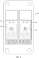
FIG. 1 comprises a schematic view of a power module as configured in accordance with various embodiments of these teachings; -
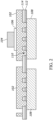
FIG. 2 comprises a partial cross-sectional view of a power module as configured in accordance with various embodiments of these teachings; -
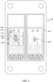
FIG. 3 comprises a schematic view of a power module as configured in accordance with various embodiments of these teachings; -
FIG. 4 comprises a partial cross-sectional view of a power module as configured in accordance with various embodiments of these teachings; -
FIG. 5 comprises a schematic view of a power module as configured in accordance with various embodiments of these teachings; -
FIG. 6 comprises a perspective view of a control circuit for a power module as configured in accordance with various embodiments of these teachings; and -
FIG. 7 comprises a flow diagram of a method in accordance with various embodiments of these teachings. - Elements in the figures are illustrated for simplicity and clarity and have not necessarily been drawn to scale. For example, the dimensions and/or relative positioning of some of the elements in the figures may be exaggerated relative to other elements to help to improve understanding of various embodiments of the present teachings. Also, common but well-understood elements that are useful or necessary in a commercially feasible embodiment are often not depicted in order to facilitate a less obstructed view of these various embodiments of the present teachings. Certain actions and/or steps may be described or depicted in a particular order of occurrence while those skilled in the art will understand that such specificity with respect to sequence is not actually required.
- Typical power modules are constructed from a plurality of transistors with a plurality of surface wire bonds on a die surface for interconnecting the transistors and control circuitry together. As such, these modules do not provide an area for direct temperature sensing on the die surface. Rather, the modules employ alternative temperature sensing from printed circuit board (PCB) control circuitry, including indirect methods such as measuring a body diode, expensive optical method, or the like. The lack of a simple direct temperature measurement method increases operational costs and limits reliability and safety.
- Generally speaking, the various aspects of the present disclosure can be employed with a power module comprising one or more power transistors and a conductive overlay for each of the one or more power transistors to provide a direct mounting surface for sensors such as a temperature sensor that can provide a direct temperature measurement for the one or more power transistors. The conductive overlay can include a well-defined metallic and stable surface that is directly connected to the power transistor die surface with short-distance metal connections. The additional surface of the conductive overlay makes it is possible to position a temperature sensor on top to provide fast and accurate sensing capability to improve reliability of module operation. This sensor can be easily wired to a PCB controller and data from the sensor can be provided to a gate board to provide for reliable module operation. The direct temperature measurement can result in increased reliability and safety when operating power modules.
- The terms and expressions used herein have the ordinary technical meaning as is accorded to such terms and expressions by persons skilled in the technical field as set forth above except where different specific meanings have otherwise been set forth herein. The word "or" when used herein shall be interpreted as having a disjunctive construction rather than a conjunctive construction unless otherwise specifically indicated. The terms "coupled," "fixed," "attached to," and the like refer to both direct coupling, fixing, or attaching, as well as indirect coupling, fixing, or attaching through one or more intermediate components or features, unless otherwise specified herein.
- The singular forms "a", "an", and "the" include plural references unless the context clearly dictates otherwise.
- Approximating language, as used herein throughout the specification and claims, is applied to modify any quantitative representation that could permissibly vary without resulting in a change in the basic function to which it is related. Accordingly, a value modified by a term or terms such as "about", "approximately", and "substantially", are not to be limited to the precise value specified. In at least some instances, the approximating language may correspond to the precision of an instrument for measuring the value, or the precision of the methods or machines for constructing or manufacturing the components and/or systems. For example, the approximating language may refer to being within a 10 percent margin.
- The foregoing and other benefits may become clearer upon making a thorough review and study of the following detailed description. Referring now to the drawings, and in particular to
FIG. 1 , apower module 100 is presented. Thepower module 100 can includeconductive overlays 102 havingtemperature sensors 104 adhered or bonded to a top surface thereof. In some embodiments, theconductive overlays 102 can include a copper or other conductive material power overlay (POL) sufficient to provide a coupling surface for thetemperature sensors 104. Such a POL configuration can provide a planar interconnection region where various system inputs and outputs and external devices can interface with one or more power transistors 108 (seeFIG. 2 ). Examples of a POL that may form theconductive overlays 102 described herein are provided inUS Patent 10,269,688 - Turning now to
FIG. 2 , a partial cross-section view of thepower module 100 is shown. Thepower module 100 can further include heatconductive epoxy 106 for bonding thetemperature sensors 104 to theconductive overlays 102. The heatconductive epoxy 106 can serve as a heat transfer medium between the top surface of theconductive overlays 102 and thetemperature sensors 104 so that thetemperature sensors 104 get consistent and accurate readings therefrom. Thetemperature sensors 104 can be attached with the heatconductive epoxy 106 on the wide, well defined, metallic, and stable surface of theconductive overlays 102. Further, the position of thetemperature sensors 104 can correspond to the highest temperature locations on theconductive overlays 102. In some embodiments, the highest temperature locations can be identified by modeling operation of thepower module 100. In some embodiments, thetemperature sensors 104 can be attached to theconductive overlays 102 over a central one of the one ormore power transistors 108, which modeling and testing indicates as the hottest location for thepower module 100. However, it will be appreciated that other locations are also contemplated and in some embodiments multiple temperature sensors may be positioned in close proximity to the same general location. - The
temperature sensors 104 can include thermocouples and/or a resistance temperature detector having a non-conductive housing. - The one or
more power transistors 108 have respective die surfaces over which theconductive overlays 102 are positioned. Thepower transistors 108 can include Silicon-carbide (SiC) MOSFETs or similar power transistors known in the art. - A
non-conductive layer 114 and anadhesive layer 112 can be positioned between theconductive overlays 102 and the one ormore power transistors 108. Thenon-conductive layer 114 can act as a dielectric layer between the respective die surfaces of thepower transistors 108 and theconductive overlays 102. Thenon-conductive layer 114 can include Kapton or other similar material. - Further, the
conductive overlays 102 can includevias 110 that electrically couple theconductive overlays 102 to the one ormore power transistors 108. In these embodiments, thevias 110 can pass through thenon-conductive layer 114 and theadhesive layer 112 to provide a direct metallic connection between theconductive overlays 102 and the one ormore power transistors 108. Additionally or alternatively, in some embodiments, one or more sintered layers can be utilized to interconnect theconductive overlays 102 to the surfaces of the one or more power transistors. - Turning now to
FIG. 3 , another schematic view of thepower module 100 is shown. As seen inFIG. 3 , in some embodiments, thepower module 100 can include additional sensors coupled to theconductive overlays 102. The additional sensors can include a plurality ofcurrent sensors 116 that are physically bonded and electrically coupled to theconductive overlays 102 to measure current flow between two of the one ormore power transistors 108 or other elements of thepower module 100. - As seen in the additional partial cross-section view of the
power module 100 ofFIG. 4 , thecurrent sensors 116 can be bonded to theconductive overlays 102 withsolder 117 and can bridge over gaps between sections of theconductive overlays 102. Thecurrent sensors 116 can include current sensing shunts that are attached to theconductive overlays 102 during an assembly process for thepower module 100. Thecurrent sensors 116 can be positioned between other current or temperature sensors or between top copper sections of theconductive overlays 102 to provide for a local current value. - In some embodiments, the
conductive overlays 102 are displaced a distance from the respective die surface of each of the plurality oftransistors 108 such that thetemperature sensors 104 and/or the plurality ofcurrent sensors 116 coupled to the top surface of theconductive overlays 102 are also displaced from the respective die surface of each of the plurality oftransistors 108 by the distance. Thevias 110 can bridge the distance to electrically couple theconductive overlay 102 to each of the one ormore power transistors 108. - The distance between the top surface of the
conductive overlays 102 to which thetemperature sensors 104 and soldercurrent sensors 116 are coupled and the top surface of thepower transistors 108 can be approximately 150um, where 100um of the distance results from a thickness of theconductive overlays 102 and 50um of the distance results from a thickness of thevias 110. The short distance between the top surface of thepower transistors 108 and the top surface of theconductive overlays 102 to which thetemperature sensors 104 are coupled can increases the accuracy of temperature measurement as compared to other indirect temperature measurement methods. In particular the close distance helps to ensure that the temperature reading closely corresponds to the actual temperature of the top surface of thepower transistors 108 because the distance limits dissipation of heat before it is read by thetemperature sensors 104 and/or limits the influence of other heat sources on the temperature value read by thetemperature sensors 104. - Turning now to
FIG. 5 another schematic of thepower module 100 is shown. As seen inFIG. 5 , thetemperature sensors 104 and the plurality ofcurrent sensors 116 can be electrically coupled to controlcircuit 118 via wires andsolder - As seen in
FIG. 6 , thecontrol circuit 118 can include a printed circuit board that can rest within a housing that contains the rest of thepower module 100. Thecontrol circuit 118 can pass signals to a gate board that is connected to thecontrol circuit 118 to assist in controlling operation of the one ormore power transistors 108. - It will be appreciated that although the embodiments of the
power module 100 shown inFIGS. 1-6 depict twoconductive overlays 102 coupled to two groups or sets of the one ormore power transistors 108, embodiments with more and fewerconductive overlays 102 are contemplated. - Turning now to
FIG. 7 , the embodiments described herein are also directed to amethod 200 of controlling thepower module 100 using thecontrol circuit 118. According to astep 202 of themethod 200, thetemperature sensors 104 directly measure a surface temperature of theconductive overlays 102 and/or thecurrent sensors 116 measure current flow. According to astep 204 of themethod 200, thecontrol circuit 118 modulates operation of the one ormore power transistors 108, which are electrically coupled to thecontrol circuit 118. - Modulating the operation of the
power transistors 108 can be based on one or more of the direct measurement of the surface temperature with thetemperature sensors 104 and the measurement of current flow from the plurality ofcurrent sensors 116. Further, modulating the operation of thepower transistors 108 can include stopping operation of one, more, or all of the one ormore power transistors 108 when the direct temperature measurement and or the current measurements exceed preconfigured threshold values. Further, modulating the operation of thepower transistors 108 can include limiting operation of one, more, or all of the one ormore power transistors 108 when the direct temperature measurement and or the current measurements exceed additionally preconfigured threshold values. Limiting the operation can include shutting down only some of the one ormore power transistors 108 and/or changing operating parameters such as switching frequency, power input or the like such that the temperature and or current measurement values will be reduced to levels consistent with normal safe operation of thepower module 100. - In some embodiments, the
current sensors 116 can measure the current from different locations on theconductive overlays 102 in parallel. In these embodiments, incremental differences in the current from each location can be monitored and when the current value at one location deviates more than a preconfigured amount from the other current values, thecontrol circuit 118 can modulate the operation of thepower transistors 108 to avoid catastrophic failure. For example, such modulation can include shutting down operation of some or allpower transistors 108. Further, in some embodiments, the control circuit can shutdown only ones of thepower transistors 108 that are linked to the current sensors whose current value exceeded the preconfigured threshold. - Further aspects of the disclosure are provided by the subject matter of the following clauses:
- A power module comprising one or more power transistors each having a respective die surface; a conductive overlay electrically coupled to each of the one or more power transistors over the respective die surface thereof; and a temperature sensor coupled to a top surface of the conductive overlay to provide a direct temperature measurement for the one or more power transistors.
- The power module of any preceding clause further comprising a current sensor physically bonded and electrically coupled to the conductive overlay to measure current flow between two of the one or more power transistors.
- The power module of any preceding clause wherein the current sensor comprises a current sensing shunt.
- The power module of any preceding clause further comprising a control circuit electrically coupled to the one or more power transistors, the temperature sensor, and the current sensor, wherein the control circuit is configured to modulate operation of the one or more power transistors based on the direct temperature measurement from the temperature sensor and the measurement of current flow.
- The power module of any preceding clause wherein modulating the operation of the one or more power transistors includes stopping operation of the one or more power transistors when at least one of the direct temperature measurement and the measurement of current flow exceeds a threshold value.
- The power module of any preceding clause wherein modulating the operation of the one or more power transistors includes limiting operation of the one or more power transistors when at least one of the direct temperature measurement and the measurement of current flow exceeds a threshold value.
- The power module of any preceding clause wherein the one or more power transistors include Silicon-carbide (SiC) MOSFETs.
- The power module of any preceding clause wherein conductive overlay is displaced a distance from the respective die surface of each of the plurality of transistors, and wherein the conductive overlay includes conductive vias that bridge the distance to electrically couple the conductive overlay to each of the one or more power transistors.
- The power module of any preceding clause wherein the temperature sensor comprises a resistance temperature detector having a non-conductive housing.
- The power module of any preceding clause wherein the temperature sensor is bonded to the conductive overlay with heat conductive epoxy.
- The power module of any preceding clause further comprising a control circuit electrically coupled to the one or more power transistors and the temperature sensor, wherein the control circuit is configured to modulate operation of the one or more power transistors based on the direct temperature measurement from the temperature sensor.
- The power module of any preceding clause wherein modulating the operation of the one or more power transistors includes stopping operation of the one or more power transistors when the direct temperature measurement exceeds a threshold value.
- The power module of any preceding clause wherein modulating the operation of the one or more power transistors includes limiting operation of the one or more power transistors when the direct temperature measurement exceeds a threshold value.
- A power module comprising a one or more power transistors each having a respective die surface; a first conductive overlay electrically coupled to a first group of the one or more power transistors over the respective die surface thereof; a second conductive overlay electrically coupled to a second group of the one or more power transistors over the respective die surface thereof; a first temperature sensor physically bonded to a top surface of the first conductive overlay to provide a direct temperature measurement for the first group of the one or more power transistors; a second temperature sensor physically bonded to a top surface of the second conductive overlay to provide a direct temperature measurement for the second group of the one or more power transistors; a plurality of current sensor physically bonded and electrically coupled to the first conductive overlay or the second conductive overlay, each of the plurality of current sensors configured to measure current flow between two of the one or more power transistors; and a control circuit electrically coupled to the one or more power transistors, the first and second temperature sensors, and the plurality of current sensors, wherein the control circuit is configured to modulate operation of the one or more power transistors based on the direct temperature measurements from the first and second temperature sensors and the measurements of current flow from the plurality of current sensors.
- The power module of any preceding clause wherein modulating the operation of the one or more power transistors includes stopping operation of the one or more power transistors when either of the direct temperature measurements exceeds a threshold value.
- The power module of any preceding clause wherein modulating the operation of the one or more power transistors includes limiting operation of the one or more power transistors when either of the direct temperature measurements exceeds a threshold value.
- The power module of any preceding clause wherein the one or more power transistors include Silicon-carbide (SiC) MOSFETs.
- The power module of any preceding clause wherein the first and the second conductive overlays are displaced a distance from the respective die surfaces of each of the one or more power transistors, and wherein the first and the second conductive overlays include conductive vias that bridge the distance to electrically couple the first and the second conductive overlays to each of the one or more power transistors.
- The power module of any preceding clause wherein the first and the second temperature sensors comprise resistance temperature detectors having non-conductive housings.
- A method comprising directly measuring a surface temperature of a conductive overlay with a temperature sensor physically bonded to a top surface of the conductive overlay, the conductive overlay being electrically coupled to a one or more power transistors over a respective die surface thereof; and modulating operation of the one or more power transistors with a control circuit electrically coupled to the one or more power transistors, wherein the modulating is based on the direct measurement of the surface temperature.
- The power module of any preceding clause wherein the conductive overlay is displaced a distance from the respective die surface of each of the plurality of transistors, and wherein at least one sintered layer bridges the distance to electrically couple the conductive overlay to each of the one or more power transistors.
- A method of manufacturing a power module comprising forming conductive overlay on a first surface of one or more power transistors; and coupling a temperature sensor to a top surface of the conductive overlay.
- The method of any preceding clause further comprising physically and electrically coupling a current sensor to the conductive overlay at a location between two different ones of the one or more power transistors.
- The method of any preceding clause further comprising coupling a non-conductive layer to the first surface of the one or more power transistors via an adhesive layer; and forming the conductive overlay over the non-conductive layer with vias that extend through the non-conductive layer and the adhesive layer to the first surface of the one or more power transistors.
- The method of any preceding clause further comprising electrically coupling the temperature sensor to a control circuit.
- The power module of any preceding clause wherein the conductive overlay is displaced a distance from the respective die surface of each of the one or more power transistors, and wherein at least one sintered layer bridges the distance to electrically couple the conductive overlay to each of the one or more power transistors.
Claims (15)
- A power module (100) comprising:a one or more power transistors (108) each having a respective die surface;a conductive overlay (102) electrically coupled to each of the one or more power transistors (108) over the respective die surface thereof; anda temperature sensor coupled to a top surface of the conductive overlay (102) to provide a direct temperature measurement for the one or more power transistors (108).
- The power module (100) of claim 1 further comprising:
a current sensor physically and electrically coupled to the conductive overlay (102) to measure current flow between two of the one or more power transistors (108). - The power module (100) of claim 2 wherein the current sensor comprises a current sensing shunt.
- The power module (100) of claim 2 or 3 further comprising:a control circuit (118) electrically coupled to the one or more power transistors (108), the temperature sensor, and the current sensor,wherein the control circuit (118) is configured to modulate operation of the one or more power transistors (108) based on the direct temperature measurement from the temperature sensor and the measurement of current flow.
- The power module (100) of claim 4 wherein modulating the operation of the one or more power transistors (108) includes stopping operation of the one or more power transistors (108) when the direct temperature measurement exceeds a threshold value.
- The power module (100) of claim 4 wherein modulating the operation of the one or more power transistors (108) includes limiting operation of the one or more power transistors (108) when the direct temperature measurement exceeds a threshold value.
- The power module (100) of any preceding claim wherein conductive overlay (102) is displaced a distance from the respective die surface of each of the one or more power transistors, and
wherein the conductive overlay (102) includes conductive vias (110) that bridge the distance to electrically couple the conductive overlay (102) to each of the one or more power transistors (108). - The power module (100) of any preceding claim, further comprising:a control circuit (118) electrically coupled to the one or more power transistors (108) and the temperature sensor,wherein the control circuit (118) is configured to modulate operation of the one or more power transistors (108) based on the direct temperature measurement from the temperature sensor.
- The power module (100) of claim 8 wherein modulating the operation of the one or more power transistors (108) includes stopping operation of the one or more power transistors (108) when the direct temperature measurement exceeds a threshold value.
- The power module (100) of claim 8 wherein modulating the operation of the one or more power transistors (108) includes limiting operation of the one or more power transistors (108) when the direct temperature measurement exceeds a threshold value.
- A method comprising:directly measuring a surface temperature of a conductive overlay (102) with a temperature sensor physically bonded to a top surface of the conductive overlay (102), the conductive overlay (102) being electrically coupled to a one or more power transistors (108) over a respective die surface thereof; andmodulating operation of the one or more power transistors (108) with a control circuit (118) electrically coupled to the one or more power transistors (108), wherein the modulating is based on the direct measurement of the surface temperature.
- A method of manufacturing a power module (100) comprising:forming conductive overlay on a first surface of one or more power transistors (108); andcoupling a temperature sensor to a top surface of the conductive overlay.
- The method of claim 12 further comprising physically and electrically coupling a current sensor to the conductive overlay at a location between two different ones of the one or more power transistors (108).
- The method of claims 12 or 13 further comprising:coupling a non-conductive layer (114) to the first surface of the one or more power transistors (108) via an adhesive layer (112); andforming the conductive overlay over the non-conductive layer (114) with vias (110) that extend through the non-conductive layer (114) and the adhesive layer (112) to the first surface of the one or more power transistors (108).
- The method of any of claims 12-14 further comprising electrically coupling the temperature sensor to a control circuit (118).
Applications Claiming Priority (1)
| Application Number | Priority Date | Filing Date | Title |
|---|---|---|---|
| US17/957,333 US20240112976A1 (en) | 2022-09-30 | 2022-09-30 | Accurate and fast power module properties assessment |
Publications (2)
| Publication Number | Publication Date |
|---|---|
| EP4345432A1 true EP4345432A1 (en) | 2024-04-03 |
| EP4345432B1 EP4345432B1 (en) | 2025-05-28 |
Family
ID=88017789
Family Applications (1)
| Application Number | Title | Priority Date | Filing Date |
|---|---|---|---|
| EP23196916.3A Active EP4345432B1 (en) | 2022-09-30 | 2023-09-12 | Accurate and fast power module temperature assessment |
Country Status (4)
| Country | Link |
|---|---|
| US (2) | US20240112976A1 (en) |
| EP (1) | EP4345432B1 (en) |
| JP (1) | JP7711142B2 (en) |
| CN (1) | CN117805569A (en) |
Citations (5)
| Publication number | Priority date | Publication date | Assignee | Title |
|---|---|---|---|---|
| US20140138807A1 (en) * | 2011-08-16 | 2014-05-22 | General Electric Company | Power overlay structure with leadframe connections |
| US10269688B2 (en) | 2013-03-14 | 2019-04-23 | General Electric Company | Power overlay structure and method of making same |
| CN112327127A (en) * | 2020-10-29 | 2021-02-05 | 西安西电电力系统有限公司 | Fully-controlled power electronic device integrated with platinum temperature sensor and junction temperature measuring method |
| US20210296217A1 (en) * | 2018-08-08 | 2021-09-23 | Agency For Science, Technology And Research | Semiconductor package and method of forming the same |
| US20220070996A1 (en) * | 2020-08-28 | 2022-03-03 | Ge Aviation Systems Llc | Power overlay module and method of assembling |
Family Cites Families (10)
| Publication number | Priority date | Publication date | Assignee | Title |
|---|---|---|---|---|
| US6930371B2 (en) * | 2003-02-03 | 2005-08-16 | International Rectifier Corporation | Temperature-sensing diode |
| US7554173B2 (en) | 2004-12-22 | 2009-06-30 | Mitsubishi Electric Corporation | Semiconductor device |
| JP4695041B2 (en) | 2006-08-09 | 2011-06-08 | 本田技研工業株式会社 | Semiconductor device |
| JP5709161B2 (en) | 2010-12-28 | 2015-04-30 | 独立行政法人産業技術総合研究所 | Power semiconductor module |
| US8730681B2 (en) * | 2011-09-23 | 2014-05-20 | Infineon Technologies Ag | Power semiconductor module with wireless saw temperature sensor |
| DE102014109816B4 (en) | 2014-07-14 | 2016-11-03 | Infineon Technologies Ag | Power semiconductor module and system with at least two power semiconductor modules |
| US11094610B2 (en) | 2017-05-30 | 2021-08-17 | Mitsubishi Electric Corporation | Semiconductor power module |
| JP7322654B2 (en) | 2019-10-15 | 2023-08-08 | 富士電機株式会社 | semiconductor module |
| JP6906583B2 (en) | 2019-10-29 | 2021-07-21 | 三菱電機株式会社 | Semiconductor power module |
| WO2021167596A1 (en) * | 2020-02-19 | 2021-08-26 | Pierburg Gmbh | Electric power module |
-
2022
- 2022-09-30 US US17/957,333 patent/US20240112976A1/en not_active Abandoned
-
2023
- 2023-09-12 EP EP23196916.3A patent/EP4345432B1/en active Active
- 2023-09-22 CN CN202311232092.1A patent/CN117805569A/en active Pending
- 2023-09-29 JP JP2023170199A patent/JP7711142B2/en active Active
-
2025
- 2025-01-16 US US19/023,798 patent/US20250157871A1/en active Pending
Patent Citations (5)
| Publication number | Priority date | Publication date | Assignee | Title |
|---|---|---|---|---|
| US20140138807A1 (en) * | 2011-08-16 | 2014-05-22 | General Electric Company | Power overlay structure with leadframe connections |
| US10269688B2 (en) | 2013-03-14 | 2019-04-23 | General Electric Company | Power overlay structure and method of making same |
| US20210296217A1 (en) * | 2018-08-08 | 2021-09-23 | Agency For Science, Technology And Research | Semiconductor package and method of forming the same |
| US20220070996A1 (en) * | 2020-08-28 | 2022-03-03 | Ge Aviation Systems Llc | Power overlay module and method of assembling |
| CN112327127A (en) * | 2020-10-29 | 2021-02-05 | 西安西电电力系统有限公司 | Fully-controlled power electronic device integrated with platinum temperature sensor and junction temperature measuring method |
Also Published As
| Publication number | Publication date |
|---|---|
| US20240112976A1 (en) | 2024-04-04 |
| JP2024052637A (en) | 2024-04-11 |
| US20250157871A1 (en) | 2025-05-15 |
| JP7711142B2 (en) | 2025-07-22 |
| EP4345432B1 (en) | 2025-05-28 |
| CN117805569A (en) | 2024-04-02 |
Similar Documents
| Publication | Publication Date | Title |
|---|---|---|
| US8596113B2 (en) | Intake air temperature sensor and thermal airflow meter including the same | |
| US10041979B2 (en) | Method of sensing current flowing in a power module | |
| US9711436B2 (en) | Multi chip module, method for operating the same and DC/DC converter | |
| US7849749B2 (en) | Pressure sensor module | |
| US11193957B2 (en) | Shunt resistor averaging techniques | |
| CN103368412A (en) | Junction temperature measurement of a power MOSFET | |
| US20170222131A1 (en) | Hall-effect sensor isolator | |
| JP2011009436A (en) | Circuit board and discharge lamp lighting device using the same | |
| KR20080097409A (en) | Electret Capacitor Type Sensor | |
| AU2009217526B2 (en) | Pressure sense die pad layout and method for direct wire bonding to programmable compensation integrated circuit die | |
| EP4345432B1 (en) | Accurate and fast power module temperature assessment | |
| TWI716447B (en) | Temperature detection device | |
| CN206223317U (en) | Temperature detection device | |
| CN101650381A (en) | Power conversion device and current detection device thereof | |
| JP2008286666A (en) | Probe card | |
| JP2015108543A (en) | Temperature detection device | |
| JP2014204003A (en) | Power supply module | |
| CN108291843A (en) | Semiconductor component with the first temperature-measuring element and the method for determining the electric current for flowing through semiconductor component | |
| CN118937724A (en) | Thermal testing tool | |
| JP6506417B2 (en) | Electronic device and electronic module | |
| JPH01113674A (en) | Current detector | |
| CN208570594U (en) | A kind of power semiconductor modular substrate and power semiconductor modular | |
| US10523126B1 (en) | Multi-section current sense method for monolithic power system | |
| CN223427943U (en) | Pump driving device based on combined board card | |
| CN220606110U (en) | Heating plate of film type integrated temperature sensor |
Legal Events
| Date | Code | Title | Description |
|---|---|---|---|
| PUAI | Public reference made under article 153(3) epc to a published international application that has entered the european phase |
Free format text: ORIGINAL CODE: 0009012 |
|
| STAA | Information on the status of an ep patent application or granted ep patent |
Free format text: STATUS: THE APPLICATION HAS BEEN PUBLISHED |
|
| AK | Designated contracting states |
Kind code of ref document: A1 Designated state(s): AL AT BE BG CH CY CZ DE DK EE ES FI FR GB GR HR HU IE IS IT LI LT LU LV MC ME MK MT NL NO PL PT RO RS SE SI SK SM TR |
|
| STAA | Information on the status of an ep patent application or granted ep patent |
Free format text: STATUS: REQUEST FOR EXAMINATION WAS MADE |
|
| GRAP | Despatch of communication of intention to grant a patent |
Free format text: ORIGINAL CODE: EPIDOSNIGR1 |
|
| STAA | Information on the status of an ep patent application or granted ep patent |
Free format text: STATUS: GRANT OF PATENT IS INTENDED |
|
| 17P | Request for examination filed |
Effective date: 20240808 |
|
| RBV | Designated contracting states (corrected) |
Designated state(s): AL AT BE BG CH CY CZ DE DK EE ES FI FR GB GR HR HU IE IS IT LI LT LU LV MC ME MK MT NL NO PL PT RO RS SE SI SK SM TR |
|
| RIC1 | Information provided on ipc code assigned before grant |
Ipc: H01L 25/07 20060101ALI20240829BHEP Ipc: H01L 25/16 20230101ALI20240829BHEP Ipc: H01L 23/538 20060101ALI20240829BHEP Ipc: H01L 23/34 20060101ALI20240829BHEP Ipc: H01L 23/053 20060101ALI20240829BHEP Ipc: G01R 31/26 20200101ALI20240829BHEP Ipc: G01K 3/00 20060101ALI20240829BHEP Ipc: H01L 29/00 20060101ALI20240829BHEP Ipc: H01L 23/00 20060101ALI20240829BHEP Ipc: G01R 31/00 20060101ALI20240829BHEP Ipc: G01R 19/00 20060101ALI20240829BHEP Ipc: G01K 7/42 20060101ALI20240829BHEP Ipc: G01K 1/143 20210101AFI20240829BHEP |
|
| INTG | Intention to grant announced |
Effective date: 20240912 |
|
| GRAJ | Information related to disapproval of communication of intention to grant by the applicant or resumption of examination proceedings by the epo deleted |
Free format text: ORIGINAL CODE: EPIDOSDIGR1 |
|
| STAA | Information on the status of an ep patent application or granted ep patent |
Free format text: STATUS: REQUEST FOR EXAMINATION WAS MADE |
|
| GRAP | Despatch of communication of intention to grant a patent |
Free format text: ORIGINAL CODE: EPIDOSNIGR1 |
|
| STAA | Information on the status of an ep patent application or granted ep patent |
Free format text: STATUS: GRANT OF PATENT IS INTENDED |
|
| INTC | Intention to grant announced (deleted) | ||
| RIC1 | Information provided on ipc code assigned before grant |
Ipc: H01L 25/07 20060101ALI20250106BHEP Ipc: H01L 25/16 20230101ALI20250106BHEP Ipc: H01L 23/538 20060101ALI20250106BHEP Ipc: H01L 23/34 20060101ALI20250106BHEP Ipc: H01L 23/053 20060101ALI20250106BHEP Ipc: G01R 31/26 20200101ALI20250106BHEP Ipc: G01K 3/00 20060101ALI20250106BHEP Ipc: H01L 23/00 20060101ALI20250106BHEP Ipc: G01R 31/00 20060101ALI20250106BHEP Ipc: G01R 19/00 20060101ALI20250106BHEP Ipc: G01K 7/42 20060101ALI20250106BHEP Ipc: G01K 1/143 20210101AFI20250106BHEP |
|
| INTG | Intention to grant announced |
Effective date: 20250116 |
|
| RIN1 | Information on inventor provided before grant (corrected) |
Inventor name: SMOLENSKI, JOSEPH Inventor name: EDDINS, RICHARD Inventor name: CHO, HYUNMIN Inventor name: GRIMES, DARRELL Inventor name: YANG, LIQIANG Inventor name: LEE, SHUNG IK |
|
| GRAS | Grant fee paid |
Free format text: ORIGINAL CODE: EPIDOSNIGR3 |
|
| GRAA | (expected) grant |
Free format text: ORIGINAL CODE: 0009210 |
|
| STAA | Information on the status of an ep patent application or granted ep patent |
Free format text: STATUS: THE PATENT HAS BEEN GRANTED |
|
| AK | Designated contracting states |
Kind code of ref document: B1 Designated state(s): AL AT BE BG CH CY CZ DE DK EE ES FI FR GB GR HR HU IE IS IT LI LT LU LV MC ME MK MT NL NO PL PT RO RS SE SI SK SM TR |
|
| REG | Reference to a national code |
Ref country code: GB Ref legal event code: FG4D |
|
| REG | Reference to a national code |
Ref country code: CH Ref legal event code: EP |
|
| REG | Reference to a national code |
Ref country code: DE Ref legal event code: R096 Ref document number: 602023003682 Country of ref document: DE |
|
| REG | Reference to a national code |
Ref country code: IE Ref legal event code: FG4D |
|
| P01 | Opt-out of the competence of the unified patent court (upc) registered |
Free format text: CASE NUMBER: APP_23904/2025 Effective date: 20250520 |
|
| REG | Reference to a national code |
Ref country code: NL Ref legal event code: MP Effective date: 20250528 |
|
| PG25 | Lapsed in a contracting state [announced via postgrant information from national office to epo] |
Ref country code: FI Free format text: LAPSE BECAUSE OF FAILURE TO SUBMIT A TRANSLATION OF THE DESCRIPTION OR TO PAY THE FEE WITHIN THE PRESCRIBED TIME-LIMIT Effective date: 20250528 Ref country code: ES Free format text: LAPSE BECAUSE OF FAILURE TO SUBMIT A TRANSLATION OF THE DESCRIPTION OR TO PAY THE FEE WITHIN THE PRESCRIBED TIME-LIMIT Effective date: 20250528 |
|
| PGFP | Annual fee paid to national office [announced via postgrant information from national office to epo] |
Ref country code: DE Payment date: 20250820 Year of fee payment: 3 |
|
| REG | Reference to a national code |
Ref country code: LT Ref legal event code: MG9D |
|
| PG25 | Lapsed in a contracting state [announced via postgrant information from national office to epo] |
Ref country code: GR Free format text: LAPSE BECAUSE OF FAILURE TO SUBMIT A TRANSLATION OF THE DESCRIPTION OR TO PAY THE FEE WITHIN THE PRESCRIBED TIME-LIMIT Effective date: 20250829 Ref country code: NO Free format text: LAPSE BECAUSE OF FAILURE TO SUBMIT A TRANSLATION OF THE DESCRIPTION OR TO PAY THE FEE WITHIN THE PRESCRIBED TIME-LIMIT Effective date: 20250828 |
|
| PG25 | Lapsed in a contracting state [announced via postgrant information from national office to epo] |
Ref country code: PL Free format text: LAPSE BECAUSE OF FAILURE TO SUBMIT A TRANSLATION OF THE DESCRIPTION OR TO PAY THE FEE WITHIN THE PRESCRIBED TIME-LIMIT Effective date: 20250528 Ref country code: NL Free format text: LAPSE BECAUSE OF FAILURE TO SUBMIT A TRANSLATION OF THE DESCRIPTION OR TO PAY THE FEE WITHIN THE PRESCRIBED TIME-LIMIT Effective date: 20250528 |
|
| PG25 | Lapsed in a contracting state [announced via postgrant information from national office to epo] |
Ref country code: BG Free format text: LAPSE BECAUSE OF FAILURE TO SUBMIT A TRANSLATION OF THE DESCRIPTION OR TO PAY THE FEE WITHIN THE PRESCRIBED TIME-LIMIT Effective date: 20250528 |
|
| PG25 | Lapsed in a contracting state [announced via postgrant information from national office to epo] |
Ref country code: HR Free format text: LAPSE BECAUSE OF FAILURE TO SUBMIT A TRANSLATION OF THE DESCRIPTION OR TO PAY THE FEE WITHIN THE PRESCRIBED TIME-LIMIT Effective date: 20250528 |
|
| PGFP | Annual fee paid to national office [announced via postgrant information from national office to epo] |
Ref country code: AT Payment date: 20251020 Year of fee payment: 3 Ref country code: FR Payment date: 20250821 Year of fee payment: 3 |
|
| PG25 | Lapsed in a contracting state [announced via postgrant information from national office to epo] |
Ref country code: RS Free format text: LAPSE BECAUSE OF FAILURE TO SUBMIT A TRANSLATION OF THE DESCRIPTION OR TO PAY THE FEE WITHIN THE PRESCRIBED TIME-LIMIT Effective date: 20250828 |
|
| PG25 | Lapsed in a contracting state [announced via postgrant information from national office to epo] |
Ref country code: IS Free format text: LAPSE BECAUSE OF FAILURE TO SUBMIT A TRANSLATION OF THE DESCRIPTION OR TO PAY THE FEE WITHIN THE PRESCRIBED TIME-LIMIT Effective date: 20250928 |
|
| PG25 | Lapsed in a contracting state [announced via postgrant information from national office to epo] |
Ref country code: LV Free format text: LAPSE BECAUSE OF FAILURE TO SUBMIT A TRANSLATION OF THE DESCRIPTION OR TO PAY THE FEE WITHIN THE PRESCRIBED TIME-LIMIT Effective date: 20250528 |
|
| REG | Reference to a national code |
Ref country code: AT Ref legal event code: MK05 Ref document number: 1798828 Country of ref document: AT Kind code of ref document: T Effective date: 20250528 |
|
| PG25 | Lapsed in a contracting state [announced via postgrant information from national office to epo] |
Ref country code: SM Free format text: LAPSE BECAUSE OF FAILURE TO SUBMIT A TRANSLATION OF THE DESCRIPTION OR TO PAY THE FEE WITHIN THE PRESCRIBED TIME-LIMIT Effective date: 20250528 Ref country code: DK Free format text: LAPSE BECAUSE OF FAILURE TO SUBMIT A TRANSLATION OF THE DESCRIPTION OR TO PAY THE FEE WITHIN THE PRESCRIBED TIME-LIMIT Effective date: 20250528 Ref country code: AT Free format text: LAPSE BECAUSE OF FAILURE TO SUBMIT A TRANSLATION OF THE DESCRIPTION OR TO PAY THE FEE WITHIN THE PRESCRIBED TIME-LIMIT Effective date: 20250528 |
|
| PG25 | Lapsed in a contracting state [announced via postgrant information from national office to epo] |
Ref country code: CZ Free format text: LAPSE BECAUSE OF FAILURE TO SUBMIT A TRANSLATION OF THE DESCRIPTION OR TO PAY THE FEE WITHIN THE PRESCRIBED TIME-LIMIT Effective date: 20250528 |
|
| PG25 | Lapsed in a contracting state [announced via postgrant information from national office to epo] |
Ref country code: EE Free format text: LAPSE BECAUSE OF FAILURE TO SUBMIT A TRANSLATION OF THE DESCRIPTION OR TO PAY THE FEE WITHIN THE PRESCRIBED TIME-LIMIT Effective date: 20250528 |
|
| PG25 | Lapsed in a contracting state [announced via postgrant information from national office to epo] |
Ref country code: SK Free format text: LAPSE BECAUSE OF FAILURE TO SUBMIT A TRANSLATION OF THE DESCRIPTION OR TO PAY THE FEE WITHIN THE PRESCRIBED TIME-LIMIT Effective date: 20250528 |
|
| PG25 | Lapsed in a contracting state [announced via postgrant information from national office to epo] |
Ref country code: IT Free format text: LAPSE BECAUSE OF FAILURE TO SUBMIT A TRANSLATION OF THE DESCRIPTION OR TO PAY THE FEE WITHIN THE PRESCRIBED TIME-LIMIT Effective date: 20250528 |
|
| REG | Reference to a national code |
Ref country code: DE Ref legal event code: R097 Ref document number: 602023003682 Country of ref document: DE |
|
| PG25 | Lapsed in a contracting state [announced via postgrant information from national office to epo] |
Ref country code: RO Free format text: LAPSE BECAUSE OF FAILURE TO SUBMIT A TRANSLATION OF THE DESCRIPTION OR TO PAY THE FEE WITHIN THE PRESCRIBED TIME-LIMIT Effective date: 20250528 |
|
| PLBE | No opposition filed within time limit |
Free format text: ORIGINAL CODE: 0009261 |
|
| STAA | Information on the status of an ep patent application or granted ep patent |
Free format text: STATUS: NO OPPOSITION FILED WITHIN TIME LIMIT |
|
| REG | Reference to a national code |
Ref country code: CH Ref legal event code: L10 Free format text: ST27 STATUS EVENT CODE: U-0-0-L10-L00 (AS PROVIDED BY THE NATIONAL OFFICE) Effective date: 20260409 |
|
| 26N | No opposition filed |
Effective date: 20260303 |