EP4343820A1 - Methods for polishing bulk silicon devices - Google Patents
Methods for polishing bulk silicon devices Download PDFInfo
- Publication number
- EP4343820A1 EP4343820A1 EP23196997.3A EP23196997A EP4343820A1 EP 4343820 A1 EP4343820 A1 EP 4343820A1 EP 23196997 A EP23196997 A EP 23196997A EP 4343820 A1 EP4343820 A1 EP 4343820A1
- Authority
- EP
- European Patent Office
- Prior art keywords
- polishing
- silicon
- slurry
- deionized water
- bulk silicon
- Prior art date
- Legal status (The legal status is an assumption and is not a legal conclusion. Google has not performed a legal analysis and makes no representation as to the accuracy of the status listed.)
- Pending
Links
Images



Classifications
-
- H—ELECTRICITY
- H10—SEMICONDUCTOR DEVICES; ELECTRIC SOLID-STATE DEVICES NOT OTHERWISE PROVIDED FOR
- H10P—GENERIC PROCESSES OR APPARATUS FOR THE MANUFACTURE OR TREATMENT OF DEVICES COVERED BY CLASS H10
- H10P90/00—Preparation of wafers not covered by a single main group of this subclass, e.g. wafer reinforcement
- H10P90/12—Preparing bulk and homogeneous wafers
- H10P90/129—Preparing bulk and homogeneous wafers by polishing
-
- H—ELECTRICITY
- H10—SEMICONDUCTOR DEVICES; ELECTRIC SOLID-STATE DEVICES NOT OTHERWISE PROVIDED FOR
- H10P—GENERIC PROCESSES OR APPARATUS FOR THE MANUFACTURE OR TREATMENT OF DEVICES COVERED BY CLASS H10
- H10P52/00—Grinding, lapping or polishing of wafers, substrates or parts of devices
- H10P52/40—Chemomechanical polishing [CMP]
- H10P52/402—Chemomechanical polishing [CMP] of semiconductor materials
-
- B—PERFORMING OPERATIONS; TRANSPORTING
- B24—GRINDING; POLISHING
- B24B—MACHINES, DEVICES, OR PROCESSES FOR GRINDING OR POLISHING; DRESSING OR CONDITIONING OF ABRADING SURFACES; FEEDING OF GRINDING, POLISHING, OR LAPPING AGENTS
- B24B37/00—Lapping machines or devices; Accessories
- B24B37/02—Lapping machines or devices; Accessories designed for working surfaces of revolution
-
- B—PERFORMING OPERATIONS; TRANSPORTING
- B24—GRINDING; POLISHING
- B24B—MACHINES, DEVICES, OR PROCESSES FOR GRINDING OR POLISHING; DRESSING OR CONDITIONING OF ABRADING SURFACES; FEEDING OF GRINDING, POLISHING, OR LAPPING AGENTS
- B24B37/00—Lapping machines or devices; Accessories
- B24B37/34—Accessories
-
- B—PERFORMING OPERATIONS; TRANSPORTING
- B24—GRINDING; POLISHING
- B24B—MACHINES, DEVICES, OR PROCESSES FOR GRINDING OR POLISHING; DRESSING OR CONDITIONING OF ABRADING SURFACES; FEEDING OF GRINDING, POLISHING, OR LAPPING AGENTS
- B24B7/00—Machines or devices designed for grinding plane surfaces on work, including polishing plane glass surfaces; Accessories therefor
- B24B7/20—Machines or devices designed for grinding plane surfaces on work, including polishing plane glass surfaces; Accessories therefor characterised by a special design with respect to properties of the material of non-metallic articles to be ground
- B24B7/22—Machines or devices designed for grinding plane surfaces on work, including polishing plane glass surfaces; Accessories therefor characterised by a special design with respect to properties of the material of non-metallic articles to be ground for grinding inorganic material, e.g. stone, ceramics, porcelain
- B24B7/228—Machines or devices designed for grinding plane surfaces on work, including polishing plane glass surfaces; Accessories therefor characterised by a special design with respect to properties of the material of non-metallic articles to be ground for grinding inorganic material, e.g. stone, ceramics, porcelain for grinding thin, brittle parts, e.g. semiconductors, wafers
-
- B—PERFORMING OPERATIONS; TRANSPORTING
- B24—GRINDING; POLISHING
- B24B—MACHINES, DEVICES, OR PROCESSES FOR GRINDING OR POLISHING; DRESSING OR CONDITIONING OF ABRADING SURFACES; FEEDING OF GRINDING, POLISHING, OR LAPPING AGENTS
- B24B9/00—Machines or devices designed for grinding edges or bevels on work or for removing burrs; Accessories therefor
- B24B9/02—Machines or devices designed for grinding edges or bevels on work or for removing burrs; Accessories therefor characterised by a special design with respect to properties of materials specific to articles to be ground
- B24B9/06—Machines or devices designed for grinding edges or bevels on work or for removing burrs; Accessories therefor characterised by a special design with respect to properties of materials specific to articles to be ground of non-metallic inorganic material, e.g. stone, ceramics, porcelain
- B24B9/065—Machines or devices designed for grinding edges or bevels on work or for removing burrs; Accessories therefor characterised by a special design with respect to properties of materials specific to articles to be ground of non-metallic inorganic material, e.g. stone, ceramics, porcelain of thin, brittle parts, e.g. semiconductors, wafers
-
- H—ELECTRICITY
- H10—SEMICONDUCTOR DEVICES; ELECTRIC SOLID-STATE DEVICES NOT OTHERWISE PROVIDED FOR
- H10P—GENERIC PROCESSES OR APPARATUS FOR THE MANUFACTURE OR TREATMENT OF DEVICES COVERED BY CLASS H10
- H10P52/00—Grinding, lapping or polishing of wafers, substrates or parts of devices
-
- H—ELECTRICITY
- H10—SEMICONDUCTOR DEVICES; ELECTRIC SOLID-STATE DEVICES NOT OTHERWISE PROVIDED FOR
- H10P—GENERIC PROCESSES OR APPARATUS FOR THE MANUFACTURE OR TREATMENT OF DEVICES COVERED BY CLASS H10
- H10P70/00—Cleaning of wafers, substrates or parts of devices
Definitions
- the technology of the disclosure relates generally to semiconductor manufacturing techniques and more particularly to polishing silicon wafers.
- Computing devices abound in modem society, and more particularly, mobile communication devices have become increasingly common.
- the prevalence of these mobile communication devices is driven in part by the many functions that are now enabled on such devices.
- Increased processing capabilities in such devices means that mobile communication devices have evolved from pure communication tools into sophisticated mobile entertainment centers, thus enabling enhanced user experiences.
- the evolution of computing devices is driven in large part by advances in the semiconductor technologies used to create integrated circuits capable of providing such functions.
- Commercial pressures to minimize power consumption, reduce size, reduce cost, or increase processing power continue to provide room for innovation in this space.
- aspects disclosed in the detailed description include methods for polishing bulk silicon devices.
- mechanical polishing is facilitated by cyclically alternating between a silicon-reactive slurry and deionized water while a mechanical polishing head operates on a surface.
- the polishing head is polishing a bulk silicon carrier wafer to expose a backside of a radio frequency (RF) complementary metal o xide semiconductor (CMOS) switch, although other semiconductors may also benefit from example aspects of the present disclosure.
- RF radio frequency
- CMOS complementary metal o xide semiconductor
- a method for exposing a device for backside processing comprises polishing the device with a silicon slurry and a polishing head.
- the method also comprises rinsing the device with deionized water to remove the silicon slurry.
- a method for exposing a device for backside processing comprises polishing a backside of a device having a thin device layer by running a continuous cycle of reactive silicon slurry and deionized water.
- a mobile terminal comprising an integrated circuit comprising a device formed from the method for exposing a device for backside processing.
- the method comprises polishing the device with a silicon slurry and a polishing head.
- the method also comprises rinsing the device with deionized water to remove the silicon slurry.
- aspects disclosed in the detailed description include methods for polishing bulk silicon devices.
- mechanical polishing is facilitated by cyclically alternating between a silicon-reactive slurry and deionized water while a mechanical polishing head operates on a surface.
- the polishing head is polishing a bulk silicon carrier wafer to expose a backside of a radio frequency (RF) complementary metal oxide semiconductor (CMOS) switch, although other semiconductors may also benefit from example aspects of the present disclosure.
- RF radio frequency
- CMOS complementary metal oxide semiconductor
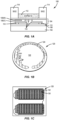
- Figure 1A is a cross-sectional side elevation view of a semiconductor device 100 that may have a carrier wafer 102 attached to a metallization layer 104 by an adhesive 106.
- the metallization layer 104 may have metal layers 108(1)-108(N) (only two shown) therein coupled by vias 110, which provide options for coupling external pads or contacts (not shown) to elements (e.g., gates, sources, drains within transistors) within a doped silicon material 112.
- Silicon oxide (SiO 2 ) insulators 114 may provide barriers between different transistors or the like.
- the semiconductor device 100 may have been mounted on a silicon on insulator (Sol) carrier.
- Sol silicon on insulator
- the insulator material in the SoI carrier provides for desired performance characteristics without the need for further processing (e.g., backside chemical mechanical polishing (CMP)).
- CMP backside chemical mechanical polishing
- SoI materials are, as of this writing, somewhat scarce, with only two major suppliers to meet the global need. Further, SoI materials are relatively expensive. This combination of factors makes it desirable to move to a different carrier.
- One such alternative carrier is a bulk silicon substrate.
- bulk silicon is processed to reveal the backside, such as through a CMP process, it is not uncommon for irregularities in the silicon to cause uneven polishing as better seen in Figure 1B , where a wafer 120 has residual silicon 122 covering portions of the wafer 120 while already having exposed portions 124.
- the wafer 120 will be subjected to additional polishing until the residual silicon 122 has been fully removed.
- damage 130 i.e., the ovals
- Example aspects of the present disclosure provide an improved polishing process that alternately polishes and rinses the wafer to interrupt a chemical reaction, thereby slowing or preventing the polishing of portions of the wafer with comparatively thin silicon coverings. More specifically, a chemical reaction more readily starts on thicker silicon, and thus, by controlling how long a silicon slurry is present on the silicon during polishing, it is possible to control what thicknesses of silicon are polished, leaving thinner silicon portions unreacted with the slurry and thus unpolished.
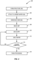
- Figure 2 is a flowchart of a process 200 according to example aspects of the present disclosure.
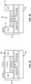
- Figures 3A-3D show various steps of the process 200 and are referred to as the process 200 is explained.
- the process 200 begins by forming a device or structure 300 in bulk silicon (block 202).
- the bulk silicon may have an initial thickness of, for example, 770 micrometers ( ⁇ m). Formation may include doping portions of the silicon to create insulators, gates, drains, sources, channels, or the like.
- the structure 300 is then attached to a carrier wafer 302 (block 204, see Figure 3A ). Note that the active elements of the structure 300 are adjacent to the carrier wafer 302 and the opposite side may be considered a backside. That is, the structure 300 may include a backside 304 formed from unused silicon material 306.
- the process 200 continues by grinding away a portion of the backside 304 (block 206). This grinding may trim the unused silicon material 306 to approximately 5-10 ⁇ m (see Figure 3B ). Of note is that the grinding step of block 206 does not expose any of the active elements of the structure 300.
- the process 200 continues by beginning CMP (block 208) by initially using a silicon slurry that is chemically reactive with the silicon material 306 (block 210) for a predefined amount of time and then purging or rinsing the backside 304 using deionized (DI) water (block 212).
- the CMP may be done using a polishing head 330 that rotates on a rotating polishing pad 332.
- the silicon slurry may be applied by opening a valve 334 to put the silicon slurry on the polishing pad 332 for a first amount of time 336 (i.e., block 210).
- valve 334 is closed and a valve 338 is opened to allow the DI water to rinse the silicon slurry off the polishing pad 332 for a second amount of time 340. Together, the times 336 and 340 form a single cycle 342.
- the valves 334, 338 may be pneumatic valves.
- a control system may determine if a predetermined number of cycles have been completed (block 214). If the answer to block 214 is no, then the process 200 returns to another slurry and rinse cycle (i.e., returns to block 210, see Figure 3C ). If, however, the answer to block 214 is yes, then the process 200 concludes with any additional processing (block 216, see Figure 3D ).
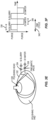
- Example aspects of the present disclosure control how much of the unused silicon material 306 is removed by controlling how long the silicon slurry is reacting with the unused silicon material 306 before the rinsing with the DI water. That is, as better seen in Figure 3G , curve 350 corresponds to relatively thick unused silicon material 306A. Because of the thickness of the unused silicon material 306A, curve 350 reflects a short incubation period 352. That is, the unused silicon material 306A begins reacting with the silicon slurry relatively quickly, and polishing by the polishing head 330 is able to remove some portion of the silicon. In contrast, the relatively thin unused silicon material 306B is slower to react to the silicon slurry and has a corresponding longer incubation period 354 shown by curve 356.
- the present disclosure can cause no reaction and no polishing of thicknesses less than the thickness corresponding to the slurry time 358. That is, each curve on the graph corresponds to a particular thickness (and there are many curves not shown), so choosing a slurry time 358 at a specific point allows all thicknesses with curves having incubation times less than the slurry time to be polished and all thicknesses with curves having incubation times greater than the slurry time to be unreacted and thus unpolished.
- the process 200 avoids polishing the silicon oxide insulators 314 while polishing out a trench 316 (see Figures 3C, 3D ).
- a graph 400 in Figure 4 may provide an alternate view of how the incubation time works.
- the rate of removal is high (i.e., fast, see curve 404).
- the rate of removal decreases.
- the silicon slurry can react with thick silicon faster than with thin silicon allowing thicker silicon to be removed by the polishing head 330 more readily.
- Example photos of a test silicon wafer 500 are shown after various numbers of cycles in Figures 5A-5D .
- the silicon material 306 is still being removed.
- some silicon has been completely removed exposing devices 502, but leaving some silicon 504.
- thirty-five cycles shown in Figure 5C
- most of the silicon 504 is gone.
- any unwanted silicon 504 is gone, leaving a predetermined thickness remaining corresponding to the thickness selected by the slurry time 358. Testing showed that the devices 502 were not damaged.
- Figure 6 is a system-level block diagram of an example mobile terminal 600 such as a smartphone, mobile computing device tablet, or the like.
- Example aspects of the present disclosure are well suited for construction of integrated circuits such as RF switches or couplers that operate in a mobile terminal 600.
- the mobile terminal 600 includes an application processor 604 (sometimes referred to as a host) that communicates with a mass storage element 606 through a universal flash storage (UFS) bus 608.
- the application processor 604 may further be connected to a display 610 through a display serial interface (DSI) bus 612 and a camera 614 through a camera serial interface (CSI) bus 616.
- Various audio elements such as a microphone 618, a speaker 620, and an audio codec 622 may be coupled to the application processor 604 through a serial low-power interchip multimedia bus (SLIMbus) 624. Additionally, the audio elements may communicate with each other through a SOUNDWIRE bus 626.
- SLIMbus serial low-power interchip multimedia bus
- a modem 628 may also be coupled to the SLIMbus 624 and/or the SOUND WIRE bus 626.
- the modem 628 may further be connected to the application processor 604 through a peripheral component interconnect (PCI) or PCI express (PCIe) bus 630 and/or a system power management interface (SPMI) bus 632.
- PCI peripheral component interconnect
- PCIe PCI express
- SPMI system power management interface
- the SPMI bus 632 may also be coupled to a local area network (LAN or WLAN) IC (LAN IC or WLAN IC) 634, a power management integrated circuit (PMIC) 636, a companion IC (sometimes referred to as a bridge chip) 638, and a radio frequency IC (RFIC) 640.
- LAN or WLAN local area network
- PMIC power management integrated circuit
- companion IC sometimes referred to as a bridge chip
- RFIC radio frequency IC
- separate PCI buses 642 and 644 may also couple the application processor 604 to the companion IC 638 and the WLAN IC 634.
- the application processor 604 may further be connected to sensors 646 through a sensor bus 648.
- the modem 628 and the RFIC 640 may communicate using a bus 650.
- the RFIC 640 may couple to one or more RFFE elements, such as an antenna tuner 652, which may include an IC formed according to example aspects of the present disclosure, a switch 654, and a power amplifier 656 through a radio frequency front end (RFFE) bus 658. Additionally, the RFIC 640 may couple to an envelope tracking power supply (ETPS) 660 through a bus 662, and the ETPS 660 may communicate with the power amplifier 656. Collectively, the RFFE elements, including the RFIC 640, may be considered an RFFE system 664. It should be appreciated that the RFFE bus 658 may be formed from a clock line and a data line (not illustrated).
- mechanical polishing is facilitated by cyclically alternating between a silicon reactive slurry and deionized water while a mechanical polishing head operates on a surface.
- the polishing head is polishing a bulk silicon carrier wafer to expose a backside of a radio frequency (RF) complementary metal oxide semiconductor (CMOS) switch, although other semiconductors may also benefit from example aspects of the present disclosure.
- RF radio frequency
- CMOS complementary metal oxide semiconductor
- a method for exposing a device for backside processing comprising: polishing the device with a silicon slurry and a polishing head; and rinsing the device with deionized water to remove the silicon slurry.
- Clause 2 The method of clause 1, further comprising repeating the polishing and rinsing for multiple cycles.
- Clause 3 The method of clause 2, further comprising selecting a residual thickness that is present after the multiple cycles by setting a slurry time.
- Clause 5 The method of clause 4, further comprising closing the valve after expiration of the slurry time.
- Clause 6 The method of any of clauses 1 to 5, wherein polishing the device with the polishing head comprises rotating the polishing head.
- Clause 7 The method of clause 6, wherein polishing the device comprising rotating a polishing pad.
- Clause 8 The method of any of clauses 1 to 7, wherein polishing the device removes a portion of the bulk silicon.
- Clause 9 The method of any of clauses 1 to 8, further comprising initially forming a structure of the device in bulk silicon.
- Clause 10 The method of clause 8 or 9, wherein forming the structure comprises forming a complementary metal oxide semiconductor.
- Clause 11 The method of clause 8, 9 or 10, wherein forming the structure comprises forming a radio frequency switch comprising a plurality of transistors.
- Clause 12 The method of any of clauses 8 to 11, further comprising adhering the structure to a carrier wafer.
- Clause 13 The method of any of clauses 1 to 12, further comprising opening a valve to apply the silicon slurry.
- Clause 14 The method of any of clauses 1 to 13, further comprising opening a valve to apply the deionized water.
- Clause 15 The method of any of clauses 1 to 14, further comprising timing the rinsing relative to the polishing a single atomic layer is removed.
- a method for exposing a device for backside processing comprising: polishing a backside of a device having a thin device layer by running a continuous cycle of reactive silicon slurry and deionized water.
- Clause 18 The method of clause 16 or 17, wherein polishing comprises removing an atomic layer of silicon by adjusting a time within the cycle of reactive silicon slurry and rinsing with deionized water.
- a mobile terminal comprising an integrated circuit comprising a device formed from the method of any of clauses 1 to 18.
Landscapes
- Engineering & Computer Science (AREA)
- Mechanical Engineering (AREA)
- Chemical & Material Sciences (AREA)
- Ceramic Engineering (AREA)
- Inorganic Chemistry (AREA)
- Mechanical Treatment Of Semiconductor (AREA)
Abstract
Description
- This application claims the benefit of
U.S. Provisional Patent Application Serial No. 63/376,463, filed on September 21, 2022 - The technology of the disclosure relates generally to semiconductor manufacturing techniques and more particularly to polishing silicon wafers.
- Computing devices abound in modem society, and more particularly, mobile communication devices have become increasingly common. The prevalence of these mobile communication devices is driven in part by the many functions that are now enabled on such devices. Increased processing capabilities in such devices means that mobile communication devices have evolved from pure communication tools into sophisticated mobile entertainment centers, thus enabling enhanced user experiences. The evolution of computing devices is driven in large part by advances in the semiconductor technologies used to create integrated circuits capable of providing such functions. Commercial pressures to minimize power consumption, reduce size, reduce cost, or increase processing power continue to provide room for innovation in this space.
- Particular aspects are set out in the appended independent claims. Various optional embodiments are set out in the dependent claims.
- Aspects disclosed in the detailed description include methods for polishing bulk silicon devices. In particular, mechanical polishing is facilitated by cyclically alternating between a silicon-reactive slurry and deionized water while a mechanical polishing head operates on a surface. In example aspects, the polishing head is polishing a bulk silicon carrier wafer to expose a backside of a radio frequency (RF) complementary metal o xide semiconductor (CMOS) switch, although other semiconductors may also benefit from example aspects of the present disclosure. While the silicon slurry is present, a reaction between the bulk silicon and the slurry takes place allowing the polishing head to remove the bulk silicon. The deionized water interrupts this reaction and helps prevent overpolishing of thin silicon layers (e.g., in trench areas) which might otherwise damage the device.
- In this regard in one aspect, a method for exposing a device for backside processing is disclosed. The method comprises polishing the device with a silicon slurry and a polishing head. The method also comprises rinsing the device with deionized water to remove the silicon slurry.
- In another aspect, a method for exposing a device for backside processing is disclosed. The method comprises polishing a backside of a device having a thin device layer by running a continuous cycle of reactive silicon slurry and deionized water.
- In another aspect, a mobile terminal comprising an integrated circuit comprising a device formed from the method for exposing a device for backside processing is disclosed. The method comprises polishing the device with a silicon slurry and a polishing head. The method also comprises rinsing the device with deionized water to remove the silicon slurry.
-
-
Figure 1A is a cross-sectional elevation view of a semiconductor device; -
Figure 1B is a top plan view of a semiconductor wafer subjected to traditional chemical mechanical polishing (CMP) steps; -
Figure 1C is a top plan view of damaged doped silicon devices in the semiconductor wafer ofFigure 1B ; -
Figure 2 is a flowchart illustrating an example process for polishing semiconductor wafers according to example aspects of the present disclosure; -
Figures 3A-3D are cross-sectional elevation views showing the steps of the process ofFigure 2 ; -
Figure 3E is a stylized representation of a polishing tool that may be used in the process ofFigure 2 ; -
Figure 3F is a graph showing the cyclical process of alternating slurry and deionized water according to the process ofFigure 2 ; -
Figure 3G is a time versus removal rate graph showing how incubation period varies by thickness of silicon along with a cross-sectional view of a wafer having different thicknesses corresponding to the curves on the graph; -
Figure 4 is a graph showing the rate of removal compared to cycles juxtaposed with a height of a silicon material showing how interruption of the chemical reaction allows for a softer polishing of a semiconductor wafer; -
Figures 5A-5D show top planned views of a semiconductor wafer after various numbers of cycles of the present disclosure; and -
Figure 6 is a block diagram of a mobile computing device which may include a semiconductor device made according to example aspects of the present disclosure. - The embodiments set forth below represent the necessary information to enable those skilled in the art to practice the embodiments and illustrate the best mode of practicing the embodiments. Upon reading the following description in light of the accompanying drawing figures, those skilled in the art will understand the concepts of the disclosure and will recognize applications of these concepts not particularly addressed herein. It should be understood that these concepts and applications fall within the scope of the disclosure and the accompanying claims.
- It will be understood that although the terms first, second, etc. may be used herein to describe various elements, these elements should not be limited by these terms. These terms are only used to distinguish one element from another. For example, a first element could be termed a second element, and, similarly, a second element could be termed a first element, without departing from the scope of the present disclosure. As used herein, the term "and/or" includes any and all combinations of one or more of the associated listed items.
- It will be understood that when an element such as a layer, region, or substrate is referred to as being "on" or extending "onto" another element, it can be directly on or extend directly onto the other element or intervening elements may also be present. In contrast, when an element is referred to as being "directly on" or extending "directly onto" another element, there are no intervening elements present. Likewise, it will be understood that when an element such as a layer, region, or substrate is referred to as being "over" or extending "over" another element, it can be directly over or extend directly over the other element or intervening elements may also be present. In contrast, when an element is referred to as being "directly over" or extending "directly over" another element, there are no intervening elements present. It will also be understood that when an element is referred to as being "connected" or "coupled" to another element, it can be directly connected or coupled to the other element or intervening elements may be present. In contrast, when an element is referred to as being "directly connected" or "directly coupled" to another element, there are no intervening elements present.
- Relative terms such as "below" or "above" or "upper" or "lower" or "horizontal" or "vertical" may be used herein to describe a relationship of one element, layer, or region to another element, layer, or region as illustrated in the Figures. It will be understood that these terms and those discussed above are intended to encompass different orientations of the device in addition to the orientation depicted in the Figures.
- The terminology used herein is for the purpose of describing particular embodiments only and is not intended to be limiting of the disclosure. As used herein, the singular forms "a," "an," and "the" are intended to include the plural forms as well, unless the context clearly indicates otherwise. It will be further understood that the terms "comprises," "comprising," "includes," and/or "including" when used herein specify the presence of stated features, integers, steps, operations, elements, and/or components, but do not preclude the presence or addition of one or more other features, integers, steps, operations, elements, components, and/or groups thereof.
- Unless otherwise defined, all terms (including technical and scientific terms) used herein have the same meaning as commonly understood by one of ordinary skill in the art to which this disclosure belongs. It will be further understood that terms used herein should be interpreted as having a meaning that is consistent with their meaning in the context of this specification and the relevant art and will not be interpreted in an idealized or overly formal sense unless expressly so defined herein.
- Aspects disclosed in the detailed description include methods for polishing bulk silicon devices. In particular, mechanical polishing is facilitated by cyclically alternating between a silicon-reactive slurry and deionized water while a mechanical polishing head operates on a surface. In example aspects, the polishing head is polishing a bulk silicon carrier wafer to expose a backside of a radio frequency (RF) complementary metal oxide semiconductor (CMOS) switch, although other semiconductors may also benefit from example aspects of the present disclosure. While the silicon slurry is present, a reaction between the bulk silicon and the slurry takes place allowing the polishing head to remove the bulk silicon. The deionized water interrupts this reaction and helps prevent overpolishing of thin silicon layers (e.g., in trench areas) which might otherwise damage the device.
- Before addressing example aspects of the present disclosure, a brief review of some of the limitations and concerns for traditional processes are provided with reference to
Figures 1A-1C . A discussion of example aspects of the present disclosure begins below with reference toFigure 2 . -
Figure 1A is a cross-sectional side elevation view of asemiconductor device 100 that may have acarrier wafer 102 attached to ametallization layer 104 by an adhesive 106. Themetallization layer 104 may have metal layers 108(1)-108(N) (only two shown) therein coupled byvias 110, which provide options for coupling external pads or contacts (not shown) to elements (e.g., gates, sources, drains within transistors) within a dopedsilicon material 112. Silicon oxide (SiO2)insulators 114 may provide barriers between different transistors or the like. - Traditionally, the
semiconductor device 100 may have been mounted on a silicon on insulator (Sol) carrier. The insulator material in the SoI carrier provides for desired performance characteristics without the need for further processing (e.g., backside chemical mechanical polishing (CMP)). SoI materials are, as of this writing, somewhat scarce, with only two major suppliers to meet the global need. Further, SoI materials are relatively expensive. This combination of factors makes it desirable to move to a different carrier. - One such alternative carrier is a bulk silicon substrate. However, to achieve the same performance, there must generally be some backside processing for devices mounted on or formed from bulk silicon substrates. When bulk silicon is processed to reveal the backside, such as through a CMP process, it is not uncommon for irregularities in the silicon to cause uneven polishing as better seen in
Figure 1B , where awafer 120 hasresidual silicon 122 covering portions of thewafer 120 while already having exposedportions 124. In general, thewafer 120 will be subjected to additional polishing until theresidual silicon 122 has been fully removed. As better seen inFigure 1C , such over polishing will result in damage 130 (i.e., the ovals) todevices 132 on thewafer 120. - Example aspects of the present disclosure provide an improved polishing process that alternately polishes and rinses the wafer to interrupt a chemical reaction, thereby slowing or preventing the polishing of portions of the wafer with comparatively thin silicon coverings. More specifically, a chemical reaction more readily starts on thicker silicon, and thus, by controlling how long a silicon slurry is present on the silicon during polishing, it is possible to control what thicknesses of silicon are polished, leaving thinner silicon portions unreacted with the slurry and thus unpolished.
- In this regard,
Figure 2 is a flowchart of aprocess 200 according to example aspects of the present disclosure.Figures 3A-3D show various steps of theprocess 200 and are referred to as theprocess 200 is explained. - The
process 200 begins by forming a device orstructure 300 in bulk silicon (block 202). The bulk silicon may have an initial thickness of, for example, 770 micrometers (µm). Formation may include doping portions of the silicon to create insulators, gates, drains, sources, channels, or the like. Thestructure 300 is then attached to a carrier wafer 302 (block 204, seeFigure 3A ). Note that the active elements of thestructure 300 are adjacent to thecarrier wafer 302 and the opposite side may be considered a backside. That is, thestructure 300 may include abackside 304 formed fromunused silicon material 306. Theprocess 200 continues by grinding away a portion of the backside 304 (block 206). This grinding may trim theunused silicon material 306 to approximately 5-10 µm (seeFigure 3B ). Of note is that the grinding step ofblock 206 does not expose any of the active elements of thestructure 300. - The
process 200 continues by beginning CMP (block 208) by initially using a silicon slurry that is chemically reactive with the silicon material 306 (block 210) for a predefined amount of time and then purging or rinsing thebackside 304 using deionized (DI) water (block 212). As better seen inFigures 3E and 3F , the CMP may be done using a polishinghead 330 that rotates on arotating polishing pad 332. The silicon slurry may be applied by opening avalve 334 to put the silicon slurry on thepolishing pad 332 for a first amount of time 336 (i.e., block 210). Atblock 212, thevalve 334 is closed and avalve 338 is opened to allow the DI water to rinse the silicon slurry off thepolishing pad 332 for a second amount oftime 340. Together, thetimes single cycle 342. In an example aspect, thevalves - With continued reference to
Figure 2 , a control system (not shown) may determine if a predetermined number of cycles have been completed (block 214). If the answer to block 214 is no, then theprocess 200 returns to another slurry and rinse cycle (i.e., returns to block 210, seeFigure 3C ). If, however, the answer to block 214 is yes, then theprocess 200 concludes with any additional processing (block 216, seeFigure 3D ). - Example aspects of the present disclosure control how much of the
unused silicon material 306 is removed by controlling how long the silicon slurry is reacting with theunused silicon material 306 before the rinsing with the DI water. That is, as better seen inFigure 3G ,curve 350 corresponds to relatively thickunused silicon material 306A. Because of the thickness of theunused silicon material 306A,curve 350 reflects ashort incubation period 352. That is, theunused silicon material 306A begins reacting with the silicon slurry relatively quickly, and polishing by the polishinghead 330 is able to remove some portion of the silicon. In contrast, the relatively thinunused silicon material 306B is slower to react to the silicon slurry and has a correspondinglonger incubation period 354 shown bycurve 356. By choosing aslurry time 358 corresponding totime 336 at a time before the incubation period of a particular thickness occurs, the present disclosure can cause no reaction and no polishing of thicknesses less than the thickness corresponding to theslurry time 358. That is, each curve on the graph corresponds to a particular thickness (and there are many curves not shown), so choosing aslurry time 358 at a specific point allows all thicknesses with curves having incubation times less than the slurry time to be polished and all thicknesses with curves having incubation times greater than the slurry time to be unreacted and thus unpolished. - By virtue of selecting an
appropriate slurry time 358, theprocess 200 avoids polishing thesilicon oxide insulators 314 while polishing out a trench 316 (seeFigures 3C, 3D ). Agraph 400 inFigure 4 may provide an alternate view of how the incubation time works. When the silicon is thick (i.e., little or no step height (curve 402)), the rate of removal is high (i.e., fast, see curve 404). As the number of cycles increases (the x-axis), the step height increases, but the rate of removal decreases. Empirically, the silicon slurry can react with thick silicon faster than with thin silicon allowing thicker silicon to be removed by the polishinghead 330 more readily. It takes the silicon slurry longer to react with the thin silicon and, since the second portion oftime 340 has the silicon slurry removed by rinsing with the DI water, there is not enough time for a large reaction to occur. The net effect of this is that the removal of thin silicon atop thesilicon oxide insulators 314 is stopped when the thickness of the silicon is decreased past the incubation period. Conversely, the thicker silicon in thetrench 316 is removed more readily so long as this silicon in thetrench 316 has a thickness with an incubation period less than theslurry time 358. Accordingly, damage to thestructure 300 is averted. The precise thickness of silicon left after the polishing is determined by selection of theslurry time 358. - Example photos of a
test silicon wafer 500 are shown after various numbers of cycles inFigures 5A-5D . Specifically, inFigure 5A , after five cycles, thesilicon material 306 is still being removed. After twenty cycles, shown inFigure 5B , some silicon has been completely removed exposingdevices 502, but leaving somesilicon 504. After thirty-five cycles, shown inFigure 5C , most of thesilicon 504 is gone. Finally, after three hundred forty-five cycles, shown inFigure 5D , anyunwanted silicon 504 is gone, leaving a predetermined thickness remaining corresponding to the thickness selected by theslurry time 358. Testing showed that thedevices 502 were not damaged. - Further testing shows that by selecting appropriate slurry reactants and by properly adjusting slurry flow, DI water flow, duty cycle, cycle time and other process parameters, the silicon can be removed with a precise control atomic layer-by-atomic layer.
- In this regard,
Figure 6 is a system-level block diagram of an examplemobile terminal 600 such as a smartphone, mobile computing device tablet, or the like. Example aspects of the present disclosure are well suited for construction of integrated circuits such as RF switches or couplers that operate in amobile terminal 600. - With continued reference to
Figure 6 , themobile terminal 600 includes an application processor 604 (sometimes referred to as a host) that communicates with amass storage element 606 through a universal flash storage (UFS)bus 608. Theapplication processor 604 may further be connected to adisplay 610 through a display serial interface (DSI)bus 612 and acamera 614 through a camera serial interface (CSI)bus 616. Various audio elements such as amicrophone 618, aspeaker 620, and anaudio codec 622 may be coupled to theapplication processor 604 through a serial low-power interchip multimedia bus (SLIMbus) 624. Additionally, the audio elements may communicate with each other through aSOUNDWIRE bus 626. Amodem 628 may also be coupled to theSLIMbus 624 and/or theSOUND WIRE bus 626. Themodem 628 may further be connected to theapplication processor 604 through a peripheral component interconnect (PCI) or PCI express (PCIe)bus 630 and/or a system power management interface (SPMI)bus 632. - With continued reference to
Figure 6 , theSPMI bus 632 may also be coupled to a local area network (LAN or WLAN) IC (LAN IC or WLAN IC) 634, a power management integrated circuit (PMIC) 636, a companion IC (sometimes referred to as a bridge chip) 638, and a radio frequency IC (RFIC) 640. It should be appreciated thatseparate PCI buses application processor 604 to thecompanion IC 638 and theWLAN IC 634. Theapplication processor 604 may further be connected tosensors 646 through asensor bus 648. Themodem 628 and theRFIC 640 may communicate using abus 650. - With continued reference to
Figure 6 , theRFIC 640 may couple to one or more RFFE elements, such as anantenna tuner 652, which may include an IC formed according to example aspects of the present disclosure, aswitch 654, and apower amplifier 656 through a radio frequency front end (RFFE)bus 658. Additionally, theRFIC 640 may couple to an envelope tracking power supply (ETPS) 660 through abus 662, and theETPS 660 may communicate with thepower amplifier 656. Collectively, the RFFE elements, including theRFIC 640, may be considered anRFFE system 664. It should be appreciated that theRFFE bus 658 may be formed from a clock line and a data line (not illustrated). - Therefore, from one perspective, there have ben described methods for polishing bulk silicon. In one aspect, mechanical polishing is facilitated by cyclically alternating between a silicon reactive slurry and deionized water while a mechanical polishing head operates on a surface. In example aspects, the polishing head is polishing a bulk silicon carrier wafer to expose a backside of a radio frequency (RF) complementary metal oxide semiconductor (CMOS) switch, although other semiconductors may also benefit from example aspects of the present disclosure. While the silicon slurry is present, a reaction between the bulk silicon and the slurry takes place allowing the polishing head to remove the bulk silicon. The deionized water interrupts this reaction and helps prevent overpolishing which might otherwise damage the device.
- Further examples are set out in the following numbered clauses.
-
Clause 1. A method for exposing a device for backside processing, the method comprising: polishing the device with a silicon slurry and a polishing head; and rinsing the device with deionized water to remove the silicon slurry. - Clause 2. The method of
clause 1, further comprising repeating the polishing and rinsing for multiple cycles. - Clause 3. The method of clause 2, further comprising selecting a residual thickness that is present after the multiple cycles by setting a slurry time.
- Clause 4. The method of clause 3, wherein setting the slurry time comprises opening a valve to release the silicon slurry for the slurry time.
- Clause 5. The method of clause 4, further comprising closing the valve after expiration of the slurry time.
- Clause 6. The method of any of
clauses 1 to 5, wherein polishing the device with the polishing head comprises rotating the polishing head. - Clause 7. The method of clause 6, wherein polishing the device comprising rotating a polishing pad.
- Clause 8. The method of any of
clauses 1 to 7, wherein polishing the device removes a portion of the bulk silicon. - Clause 9. The method of any of
clauses 1 to 8, further comprising initially forming a structure of the device in bulk silicon. -
Clause 10. The method of clause 8 or 9, wherein forming the structure comprises forming a complementary metal oxide semiconductor. - Clause 11. The method of
clause 8, 9 or 10, wherein forming the structure comprises forming a radio frequency switch comprising a plurality of transistors. - Clause 12. The method of any of clauses 8 to 11, further comprising adhering the structure to a carrier wafer.
- Clause 13. The method of any of
clauses 1 to 12, further comprising opening a valve to apply the silicon slurry. - Clause 14. The method of any of
clauses 1 to 13, further comprising opening a valve to apply the deionized water. - Clause 15. The method of any of
clauses 1 to 14, further comprising timing the rinsing relative to the polishing a single atomic layer is removed. - Clause 16. A method for exposing a device for backside processing, the method comprising: polishing a backside of a device having a thin device layer by running a continuous cycle of reactive silicon slurry and deionized water.
- Clause 17. The method of clause 16, wherein the thin device layer is a trench.
- Clause 18. The method of clause 16 or 17, wherein polishing comprises removing an atomic layer of silicon by adjusting a time within the cycle of reactive silicon slurry and rinsing with deionized water.
- Clause 19. A mobile terminal comprising an integrated circuit comprising a device formed from the method of any of
clauses 1 to 18. - It is also noted that the operational steps described in any of the example aspects herein are described to provide examples and discussion. The operations described may be performed in numerous different sequences other than the illustrated sequences. Furthermore, operations described in a single operational step may actually be performed in a number of different steps. Additionally, one or more operational steps discussed in the example aspects may be combined. It is to be understood that the operational steps illustrated in the flowchart diagrams may be subject to numerous different modifications as will be readily apparent to one of skill in the art. Those of skill in the art will also understand that information and signals may be represented using any of a variety of different technologies and techniques. For example, data, instructions, commands, information, signals, bits, symbols, and chips that may be referenced throughout the above description may be represented by voltages, currents, electromagnetic waves, magnetic fields or particles, optical fields or particles, or any combination thereof.
- The previous description of the disclosure is provided to enable any person skilled in the art to make or use the disclosure. Various modifications to the disclosure will be readily apparent to those skilled in the art, and the generic principles defined herein may be applied to other variations. Thus, the disclosure is not intended to be limited to the examples and designs described herein but is to be accorded the widest scope consistent with the principles and novel features disclosed herein.
Claims (15)
- A method for exposing a device for backside processing, the method comprising:polishing the device with a silicon slurry and a polishing head; andrinsing the device with deionized water to remove the silicon slurry.
- The method of claim 1, further comprising repeating the polishing and rinsing for multiple cycles.
- The method of claim 2, further comprising selecting a residual thickness that is present after the multiple cycles by setting a slurry time.
- The method of claim 3, wherein setting the slurry time comprises opening a valve to release the silicon slurry for the slurry time, and for example further comprising closing the valve after expiration of the slurry time.
- The method of any of claims 1 to 4, wherein polishing the device with the polishing head comprises rotating the polishing head, for example wherein polishing the device comprising rotating a polishing pad.
- The method of any of claims 1 to 5, further comprising initially forming a structure of the device in bulk silicon, for example wherein polishing the device removes a portion of the bulk silicon.
- The method of claim 6, wherein forming the structure comprises forming a complementary metal oxide semiconductor.
- The method of claim 6 or 7, wherein forming the structure comprises forming a radio frequency switch comprising a plurality of transistors.
- The method of any of claims 6 to 8, further comprising adhering the structure to a carrier wafer.
- The method of any of claims 1 to 9, further comprising opening a valve to apply the silicon slurry.
- The method of any of claims 1 to 10, further comprising opening a valve to apply the deionized water.
- The method of any of claims 1 to 11, further comprising controlling the timing of the rinsing relative to the polishing to remove a single atomic layer.
- A method for exposing a device for backside processing, the method comprising:
polishing a backside of a device, such as a trench, having a thin device layer by running a continuous cycle of reactive silicon slurry and deionized water. - The method of claim 13, wherein polishing comprises removing an atomic layer of silicon by adjusting a time within the cycle of reactive silicon slurry and rinsing with deionized water.
- A mobile terminal comprising an integrated circuit comprising a device formed from the method of any of claims 1 to 14.
Applications Claiming Priority (2)
| Application Number | Priority Date | Filing Date | Title |
|---|---|---|---|
| US202263376463P | 2022-09-21 | 2022-09-21 | |
| US18/217,694 US12622195B2 (en) | 2022-09-21 | 2023-07-03 | Methods for polishing bulk silicon devices |
Publications (1)
| Publication Number | Publication Date |
|---|---|
| EP4343820A1 true EP4343820A1 (en) | 2024-03-27 |
Family
ID=88017863
Family Applications (1)
| Application Number | Title | Priority Date | Filing Date |
|---|---|---|---|
| EP23196997.3A Pending EP4343820A1 (en) | 2022-09-21 | 2023-09-12 | Methods for polishing bulk silicon devices |
Country Status (4)
| Country | Link |
|---|---|
| US (1) | US12622195B2 (en) |
| EP (1) | EP4343820A1 (en) |
| KR (1) | KR20240040621A (en) |
| TW (1) | TW202430323A (en) |
Citations (8)
| Publication number | Priority date | Publication date | Assignee | Title |
|---|---|---|---|---|
| EP0357205A1 (en) * | 1988-07-28 | 1990-03-07 | Fujitsu Limited | Polishing liquid for polishing semiconductor substrate and polishing process |
| US5366924A (en) * | 1992-03-16 | 1994-11-22 | At&T Bell Laboratories | Method of manufacturing an integrated circuit including planarizing a wafer |
| US20030109200A1 (en) * | 2001-08-31 | 2003-06-12 | Hall Stacy W. | Constant pH polish and scrub |
| US20030190810A1 (en) * | 2002-04-05 | 2003-10-09 | Seh America, Inc. | Method of reducing particulate contamination during polishing of a wafer |
| KR100728887B1 (en) * | 2005-12-20 | 2007-06-14 | 주식회사 실트론 | Silicon Wafer Double Side Polishing Method |
| US20100081279A1 (en) * | 2008-09-30 | 2010-04-01 | Dupont Air Products Nanomaterials Llc | Method for Forming Through-base Wafer Vias in Fabrication of Stacked Devices |
| CN102208486A (en) * | 2011-04-18 | 2011-10-05 | 晶澳(扬州)太阳能科技有限公司 | Preparation method of MWT (Metal Wrap Through) solar cell |
| US20170309494A1 (en) * | 2014-07-25 | 2017-10-26 | Applied Materials, Inc. | Chemical mechanical polishing apparatus and methods |
Family Cites Families (12)
| Publication number | Priority date | Publication date | Assignee | Title |
|---|---|---|---|---|
| JP4456308B2 (en) * | 2001-12-05 | 2010-04-28 | 富士通マイクロエレクトロニクス株式会社 | Chemical supply device |
| US8263497B2 (en) * | 2009-01-13 | 2012-09-11 | International Business Machines Corporation | High-yield method of exposing and contacting through-silicon vias |
| US9368367B2 (en) * | 2009-04-13 | 2016-06-14 | Sinmat, Inc. | Chemical mechanical polishing of silicon carbide comprising surfaces |
| KR101620767B1 (en) | 2011-10-28 | 2016-05-12 | 인텔 코포레이션 | 3d interconnect structure comprising fine pitch single damascene backside metal redistribution lines combined with through-silicon vias |
| US8628990B1 (en) * | 2012-09-27 | 2014-01-14 | Taiwan Semiconductor Manufacturing Company, Ltd. | Image device and methods of forming the same |
| DE102013213839A1 (en) * | 2013-07-15 | 2015-01-15 | Siltronic Ag | Process for producing a highly doped semiconductor wafer |
| KR20150143151A (en) * | 2014-06-13 | 2015-12-23 | 삼성전자주식회사 | Method for polishing substrate |
| US10312128B2 (en) | 2015-12-31 | 2019-06-04 | Taiwan Semiconductor Manufacturing Company Ltd. | Chemical-mechanical polish (CMP) devices, tools, and methods |
| US11078380B2 (en) * | 2017-07-10 | 2021-08-03 | Entegris, Inc. | Hard abrasive particle-free polishing of hard materials |
| US10665494B2 (en) | 2018-01-31 | 2020-05-26 | Applied Materials, Inc. | Automated apparatus to temporarily attach substrates to carriers without adhesives for processing |
| US12231109B2 (en) | 2020-08-14 | 2025-02-18 | Qorvo Us, Inc. | Electronic device with solder interconnect and multiple material encapsulant |
| US11264457B1 (en) * | 2020-11-20 | 2022-03-01 | Globalfoundries U.S. Inc. | Isolation trenches augmented with a trap-rich layer |
-
2023
- 2023-07-03 US US18/217,694 patent/US12622195B2/en active Active
- 2023-08-23 TW TW112131672A patent/TW202430323A/en unknown
- 2023-08-29 KR KR1020230113632A patent/KR20240040621A/en active Pending
- 2023-09-12 EP EP23196997.3A patent/EP4343820A1/en active Pending
Patent Citations (8)
| Publication number | Priority date | Publication date | Assignee | Title |
|---|---|---|---|---|
| EP0357205A1 (en) * | 1988-07-28 | 1990-03-07 | Fujitsu Limited | Polishing liquid for polishing semiconductor substrate and polishing process |
| US5366924A (en) * | 1992-03-16 | 1994-11-22 | At&T Bell Laboratories | Method of manufacturing an integrated circuit including planarizing a wafer |
| US20030109200A1 (en) * | 2001-08-31 | 2003-06-12 | Hall Stacy W. | Constant pH polish and scrub |
| US20030190810A1 (en) * | 2002-04-05 | 2003-10-09 | Seh America, Inc. | Method of reducing particulate contamination during polishing of a wafer |
| KR100728887B1 (en) * | 2005-12-20 | 2007-06-14 | 주식회사 실트론 | Silicon Wafer Double Side Polishing Method |
| US20100081279A1 (en) * | 2008-09-30 | 2010-04-01 | Dupont Air Products Nanomaterials Llc | Method for Forming Through-base Wafer Vias in Fabrication of Stacked Devices |
| CN102208486A (en) * | 2011-04-18 | 2011-10-05 | 晶澳(扬州)太阳能科技有限公司 | Preparation method of MWT (Metal Wrap Through) solar cell |
| US20170309494A1 (en) * | 2014-07-25 | 2017-10-26 | Applied Materials, Inc. | Chemical mechanical polishing apparatus and methods |
Also Published As
| Publication number | Publication date |
|---|---|
| KR20240040621A (en) | 2024-03-28 |
| US12622195B2 (en) | 2026-05-05 |
| TW202430323A (en) | 2024-08-01 |
| US20240096636A1 (en) | 2024-03-21 |
Similar Documents
| Publication | Publication Date | Title |
|---|---|---|
| US6180020B1 (en) | Polishing method and apparatus | |
| US6245677B1 (en) | Backside chemical etching and polishing | |
| KR101139054B1 (en) | Method of the double sided polishing of a semiconductor wafer | |
| WO2001062436A1 (en) | Method and apparatus for polishing outer peripheral chamfered part of wafer | |
| CN105161418B (en) | A kind of semiconductor devices and preparation method thereof and electronic device | |
| US12622195B2 (en) | Methods for polishing bulk silicon devices | |
| EP1022778A1 (en) | Method of dividing a wafer and method of manufacturing a semiconductor device | |
| HK40103512A (en) | Methods for polishing bulk silicon devices | |
| CN117747423A (en) | Method for polishing bulk silicon device | |
| US20250154000A1 (en) | Methods for wafer bonding | |
| EP1212170B1 (en) | Method and system for chemical mechanical polishing with a cylindrical polishing pad | |
| CN212601122U (en) | Polishing pad and polishing equipment | |
| JP2000340530A (en) | Semiconductor device and manufacturing method thereof | |
| JPH10256201A (en) | Semiconductor manufacturing method | |
| US6863595B1 (en) | Methods for polishing a semiconductor topography | |
| CN110364470A (en) | Carrier for chip packaging and chip packaging method | |
| JP3798760B2 (en) | Method for forming semiconductor wafer | |
| US20220336418A1 (en) | Semiconductor structure and manufacturing method thereof | |
| KR101749482B1 (en) | Semiconductor package sliming apparatus and method of the same | |
| CN109262446A (en) | A kind of chemical and mechanical grinding method and chemical mechanical polishing device | |
| KR20020040913A (en) | Method for preventing damage to wafers in a sequential multiple steps polishing process | |
| JP3435165B2 (en) | Polishing method and polishing apparatus | |
| EP1308243B1 (en) | Polishing method | |
| US20070032176A1 (en) | Method for polishing diamond wafers | |
| KR101759125B1 (en) | Semiconductor package sliming apparatus and method of the same |
Legal Events
| Date | Code | Title | Description |
|---|---|---|---|
| PUAI | Public reference made under article 153(3) epc to a published international application that has entered the european phase |
Free format text: ORIGINAL CODE: 0009012 |
|
| STAA | Information on the status of an ep patent application or granted ep patent |
Free format text: STATUS: THE APPLICATION HAS BEEN PUBLISHED |
|
| AK | Designated contracting states |
Kind code of ref document: A1 Designated state(s): AL AT BE BG CH CY CZ DE DK EE ES FI FR GB GR HR HU IE IS IT LI LT LU LV MC ME MK MT NL NO PL PT RO RS SE SI SK SM TR |
|
| STAA | Information on the status of an ep patent application or granted ep patent |
Free format text: STATUS: REQUEST FOR EXAMINATION WAS MADE |
|
| 17P | Request for examination filed |
Effective date: 20240909 |
|
| RBV | Designated contracting states (corrected) |
Designated state(s): AL AT BE BG CH CY CZ DE DK EE ES FI FR GB GR HR HU IE IS IT LI LT LU LV MC ME MK MT NL NO PL PT RO RS SE SI SK SM TR |