EP4340147A2 - Electronic device housing, electronic device comprising said electronic device housing and method of assembling said electronic device - Google Patents
Electronic device housing, electronic device comprising said electronic device housing and method of assembling said electronic device Download PDFInfo
- Publication number
- EP4340147A2 EP4340147A2 EP24155862.6A EP24155862A EP4340147A2 EP 4340147 A2 EP4340147 A2 EP 4340147A2 EP 24155862 A EP24155862 A EP 24155862A EP 4340147 A2 EP4340147 A2 EP 4340147A2
- Authority
- EP
- European Patent Office
- Prior art keywords
- electronic device
- outer housing
- housing member
- protective side
- glass
- Prior art date
- Legal status (The legal status is an assumption and is not a legal conclusion. Google has not performed a legal analysis and makes no representation as to the accuracy of the status listed.)
- Pending
Links
- 238000000034 method Methods 0.000 title description 42
- 230000001681 protective effect Effects 0.000 claims abstract description 213
- 239000002861 polymer material Substances 0.000 claims abstract 6
- 239000011521 glass Substances 0.000 claims description 162
- 239000000853 adhesive Substances 0.000 claims description 116
- 230000001070 adhesive effect Effects 0.000 claims description 116
- 239000012790 adhesive layer Substances 0.000 claims description 18
- 239000003365 glass fiber Substances 0.000 claims description 9
- 239000007769 metal material Substances 0.000 claims 1
- 230000002093 peripheral effect Effects 0.000 description 107
- 229920000642 polymer Polymers 0.000 description 38
- 238000000465 moulding Methods 0.000 description 37
- 239000010410 layer Substances 0.000 description 31
- 239000000463 material Substances 0.000 description 21
- 239000002184 metal Substances 0.000 description 20
- 230000015572 biosynthetic process Effects 0.000 description 12
- 238000010586 diagram Methods 0.000 description 12
- 239000004033 plastic Substances 0.000 description 10
- 229920003023 plastic Polymers 0.000 description 10
- -1 e.g. Substances 0.000 description 9
- 239000004677 Nylon Substances 0.000 description 8
- 229920001778 nylon Polymers 0.000 description 8
- 239000004417 polycarbonate Substances 0.000 description 8
- 229920000515 polycarbonate Polymers 0.000 description 8
- 229920001169 thermoplastic Polymers 0.000 description 8
- 239000004416 thermosoftening plastic Substances 0.000 description 8
- 230000003139 buffering effect Effects 0.000 description 7
- 238000000151 deposition Methods 0.000 description 6
- 239000000654 additive Substances 0.000 description 4
- 230000000712 assembly Effects 0.000 description 4
- 238000000429 assembly Methods 0.000 description 4
- 230000008901 benefit Effects 0.000 description 4
- 238000005516 engineering process Methods 0.000 description 3
- 239000000126 substance Substances 0.000 description 3
- 239000000919 ceramic Substances 0.000 description 2
- 239000011248 coating agent Substances 0.000 description 2
- 238000000576 coating method Methods 0.000 description 2
- 239000000835 fiber Substances 0.000 description 2
- 239000002245 particle Substances 0.000 description 2
- 229920001343 polytetrafluoroethylene Polymers 0.000 description 2
- 239000004810 polytetrafluoroethylene Substances 0.000 description 2
- 230000000996 additive effect Effects 0.000 description 1
- 239000002313 adhesive film Substances 0.000 description 1
- 238000012986 modification Methods 0.000 description 1
- 230000004048 modification Effects 0.000 description 1
- 239000012778 molding material Substances 0.000 description 1
- 229920001721 polyimide Polymers 0.000 description 1
- 230000002787 reinforcement Effects 0.000 description 1
- 238000007650 screen-printing Methods 0.000 description 1
Images


Classifications
-
- G—PHYSICS
- G06—COMPUTING; CALCULATING OR COUNTING
- G06F—ELECTRIC DIGITAL DATA PROCESSING
- G06F1/00—Details not covered by groups G06F3/00 - G06F13/00 and G06F21/00
- G06F1/16—Constructional details or arrangements
- G06F1/1613—Constructional details or arrangements for portable computers
- G06F1/1626—Constructional details or arrangements for portable computers with a single-body enclosure integrating a flat display, e.g. Personal Digital Assistants [PDAs]
-
- H—ELECTRICITY
- H02—GENERATION; CONVERSION OR DISTRIBUTION OF ELECTRIC POWER
- H02G—INSTALLATION OF ELECTRIC CABLES OR LINES, OR OF COMBINED OPTICAL AND ELECTRIC CABLES OR LINES
- H02G11/00—Arrangements of electric cables or lines between relatively-movable parts
- H02G11/02—Arrangements of electric cables or lines between relatively-movable parts using take-up reel or drum
-
- H—ELECTRICITY
- H05—ELECTRIC TECHNIQUES NOT OTHERWISE PROVIDED FOR
- H05K—PRINTED CIRCUITS; CASINGS OR CONSTRUCTIONAL DETAILS OF ELECTRIC APPARATUS; MANUFACTURE OF ASSEMBLAGES OF ELECTRICAL COMPONENTS
- H05K5/00—Casings, cabinets or drawers for electric apparatus
- H05K5/02—Details
- H05K5/03—Covers
-
- A—HUMAN NECESSITIES
- A45—HAND OR TRAVELLING ARTICLES
- A45C—PURSES; LUGGAGE; HAND CARRIED BAGS
- A45C11/00—Receptacles for purposes not provided for in groups A45C1/00-A45C9/00
-
- A—HUMAN NECESSITIES
- A45—HAND OR TRAVELLING ARTICLES
- A45F—TRAVELLING OR CAMP EQUIPMENT: SACKS OR PACKS CARRIED ON THE BODY
- A45F5/00—Holders or carriers for hand articles; Holders or carriers for use while travelling or camping
-
- G—PHYSICS
- G06—COMPUTING; CALCULATING OR COUNTING
- G06F—ELECTRIC DIGITAL DATA PROCESSING
- G06F1/00—Details not covered by groups G06F3/00 - G06F13/00 and G06F21/00
- G06F1/16—Constructional details or arrangements
- G06F1/1613—Constructional details or arrangements for portable computers
- G06F1/1633—Constructional details or arrangements of portable computers not specific to the type of enclosures covered by groups G06F1/1615 - G06F1/1626
- G06F1/1656—Details related to functional adaptations of the enclosure, e.g. to provide protection against EMI, shock, water, or to host detachable peripherals like a mouse or removable expansions units like PCMCIA cards, or to provide access to internal components for maintenance or to removable storage supports like CDs or DVDs, or to mechanically mount accessories
-
- G—PHYSICS
- G06—COMPUTING; CALCULATING OR COUNTING
- G06F—ELECTRIC DIGITAL DATA PROCESSING
- G06F3/00—Input arrangements for transferring data to be processed into a form capable of being handled by the computer; Output arrangements for transferring data from processing unit to output unit, e.g. interface arrangements
- G06F3/01—Input arrangements or combined input and output arrangements for interaction between user and computer
- G06F3/03—Arrangements for converting the position or the displacement of a member into a coded form
- G06F3/041—Digitisers, e.g. for touch screens or touch pads, characterised by the transducing means
-
- H—ELECTRICITY
- H04—ELECTRIC COMMUNICATION TECHNIQUE
- H04M—TELEPHONIC COMMUNICATION
- H04M1/00—Substation equipment, e.g. for use by subscribers
- H04M1/02—Constructional features of telephone sets
- H04M1/0202—Portable telephone sets, e.g. cordless phones, mobile phones or bar type handsets
- H04M1/0249—Details of the mechanical connection between the housing parts or relating to the method of assembly
-
- H—ELECTRICITY
- H04—ELECTRIC COMMUNICATION TECHNIQUE
- H04M—TELEPHONIC COMMUNICATION
- H04M1/00—Substation equipment, e.g. for use by subscribers
- H04M1/02—Constructional features of telephone sets
- H04M1/0202—Portable telephone sets, e.g. cordless phones, mobile phones or bar type handsets
- H04M1/026—Details of the structure or mounting of specific components
- H04M1/0266—Details of the structure or mounting of specific components for a display module assembly
-
- H—ELECTRICITY
- H05—ELECTRIC TECHNIQUES NOT OTHERWISE PROVIDED FOR
- H05K—PRINTED CIRCUITS; CASINGS OR CONSTRUCTIONAL DETAILS OF ELECTRIC APPARATUS; MANUFACTURE OF ASSEMBLAGES OF ELECTRICAL COMPONENTS
- H05K5/00—Casings, cabinets or drawers for electric apparatus
- H05K5/0017—Casings, cabinets or drawers for electric apparatus with operator interface units
-
- G—PHYSICS
- G06—COMPUTING; CALCULATING OR COUNTING
- G06F—ELECTRIC DIGITAL DATA PROCESSING
- G06F2200/00—Indexing scheme relating to G06F1/04 - G06F1/32
- G06F2200/16—Indexing scheme relating to G06F1/16 - G06F1/18
- G06F2200/163—Indexing scheme relating to constructional details of the computer
- G06F2200/1631—Panel PC, e.g. single housing hosting PC and display panel
Definitions
- a portable electronic device has a housing that encases the various electrical components of the portable electronic device.
- the portable electronic device has a display arrangement that includes various layers.
- the various layers usually include at least a display technology layer, and may additionally include a sensing arrangement (e.g., touch sensors or touch screen) and/or a cover window disposed over the display technology layer.
- the cover window can be a plastic or glass cover that provides a protective outer surface that protects the display technology layer.
- the cover window can form part of an outer surface for the housing of the portable electronic device. Conventionally, supporting or securing the cover window to other portions of the housing tends to impede usage of a peripheral area of the cover window.
- the invention pertains to an electronic device having an enclosure formed from at least one glass cover and a peripheral structure formed adjacent the periphery of the glass cover.
- the peripheral structure can be secured adjacent to the glass cover with an adhesive.
- the peripheral structure can be molded adjacent the glass cover so that a gapless interface is formed between the peripheral structure and the periphery of the glass cover.
- the peripheral structure can include at least an inner peripheral structure and an outer peripheral structure.
- the enclosure for the electronic device is can be thin yet be sufficiently strong to be suitable for use in electronic devices, such as portable electronic devices.
- the invention can be implemented in numerous ways, including as a method, system, device, or apparatus. Several embodiments of the invention are discussed below.
- one embodiment can, for example, include at least a glass cover for a top surface for the electronic device enclosure, an adhesive deposited around a periphery of the glass cover, and a peripheral structure for providing a support surface for the glass cover and for providing side protective surfaces for the glass cover.
- the peripheral structure is at least partially secured to the glass cover by the adhesive.
- one embodiment of the method can, for example, include at least: obtaining a glass member having a top surface and a bottom surface, the top surface providing an outer surface for substantially all of a surface of the electronic device; depositing an adhesive layer around a periphery of the bottom surface of the glass member; aligning the glass member relative to a support structure for the electronic device; and molding a peripheral protective side portion for the electronic device, the peripheral protective side portion being molded adjacent the periphery of the glass member, adjacent the adhesive layer, and adjacent the support structure.
- one embodiment of the method can, for example, include at least: obtaining a glass member having a top surface and a bottom surface, the top surface providing an outer surface for substantially all of a surface of the electronic device; attaching an internal periphery member to a periphery of the bottom surface of the glass member; and molding an outer periphery member adjacent a periphery of the glass member and adjacent the internal periphery member.
- one embodiment of the method can, for example, include at least: obtaining a glass member having a top surface and a bottom surface, the top surface providing an outer surface for substantially all of a surface of the electronic device; providing an adhesive layer around a periphery of the bottom surface of the glass member; and molding a peripheral protective side portion for the electronic device.
- the peripheral protective side portion being molded adjacent the periphery of the glass member and being secured to the glass member via the adhesive layer.
- Embodiments are described herein in the context of a housing for an electronic device.
- the housing can make use of an outer member, which can be formed of glass.
- the outer member can be aligned, protected and/or secured with respect to other portions of the housing for the electronic device.
- the electronic device can be portable and in some cases handheld.
- the invention pertains to an electronic device having an enclosure formed from at least one glass cover and a peripheral structure formed adjacent the periphery of the glass cover.
- the peripheral structure can be secured adjacent to the glass cover with an adhesive.
- the peripheral structure can be molded adjacent the glass cover so that a gapless interface is formed between the peripheral structure and the periphery of the glass cover.
- the peripheral structure includes at least an inner peripheral structure and an outer peripheral structure.
- Embodiments of the invention can relate to apparatus, systems and methods for forming a housing having a thin glass member for an electronic device.
- the glass member may be an outer surface of an electronic device.
- the glass member may for example correspond to a glass cover that helps form part of a display area of an electronic device (i.e., situated in front of a display either as a separate part or integrated within the display.
- the glass member may form a part of the housing. For example, it may form an outer surface other than in the display area.
- the apparatus, systems and methods for improving strength of thin glass are especially suitable for glass covers, or displays (e.g., LCD displays), assembled in small form factor electronic devices such as handheld electronic devices (e.g., mobile phones, media players, personal digital assistants, remote controls, etc.).
- the glass can be thin in these small form factor embodiments, such as less than 3 mm, or more particularly between 0.5 and 2.5 mm, or even more particularly between 0.3 and 1.0 mm.
- the apparatus, systems and methods can also be used for glass covers or displays for other devices including, but not limited to including, relatively larger form factor electronic devices (e.g., portable computers, tablet computers, displays, monitors, televisions, etc.).
- the glass can also be thin in these larger form factor embodiments, such as less than 5 mm, or more particularly between 0.5 and 3 mm, or even more particularly between 0.3 and 2.0 mm.
- FIG. 1 a flow diagram of a housing formation process 100 according to one embodiment of the invention.
- the housing formation process 100 can operate to produce a housing for an electronic device, or at least a portion of such a housing.
- the housing formation process 100 can initially obtain 102 a glass member.
- the glass member is to serve as a significant outer surface for the housing.
- the glass member can correspond to a top surface for the housing.
- the glass member can correspond to a bottom surface for the housing.
- the glass member is typically thin, particularly when used with portable electronic devices. In one embodiment, the glass member has a thickness of less than 5 mm, or more particularly less than 1 mm.
- an adhesive can be deposited 104 around a periphery of a bottom surface of the glass member.
- the glass member has a top surface that can represent an outer surface for the housing, and a bottom surface that is an inner surface that is not exposed.
- the adhesive being deposited 104 can be a thermally activated adhesive.
- the adhesive can, for example, by provided as film or as a layer. Also, the manner by which the adhesive is deposited can vary.
- the adhesive can be deposited 104 by forming a ring-like pattern of adhesive that can be placed around the periphery of the bottom surface of the glass member.
- the adhesive can be screen printed onto the periphery of the bottom surface of the glass member.
- the glass member can be aligned 106 relative to a support structure.
- the support structure can be provided as being a component of the housing for the electronic device.
- the support can pertain to a side structure for the housing or an interior support member.
- a peripheral protective side portion can be molded 108 adjacent to the periphery of the glass member and adjacent to the adhesive.
- the adhesive can serve to secure the peripheral protective side member to the glass member.
- the peripheral protective side member being molded 108 can also be formed adjacent the support structure.
- the peripheral side portion would also be secured to the support structure by chemical bonding and/or mechanical features (e.g., undercuts or interlocks).
- the glass member and the peripheral protective side member are secured to the support structure and thus form at least a portion of the housing for the electronic device.
- the adhesive is thermally activated
- the molding 108 can also serve to activate the thermally activated adhesive so that a strong bond can be provided to the glass member and the peripheral protective side manner.
- FIG. 2A is a cross-sectional view of an electronic device housing 200 according to one embodiment.
- the electronic device housing 200 includes an outer housing member 201 supported and protected by a protective side member 202.
- the protective side member 202 being positioned tightly adjacent sides of the outer housing member 201.
- the protective side members 202 can provide a thin layer of material positioned tightly adjacent sides of the outer housing member 201, thereby buffering impact at the sides of the outer housing member 201.
- the protective side member 202 also supports the outer housing member 201 and serves to secure the outer housing member 201 to other portions of the electronic device housing 200.
- the protective side member 202 extends around all sides of the outer housing member 201.
- the protective side member 202 extends around those of the sides of the outer housing member 201 that would otherwise be exposed.
- the outer housing member 201 can be secured to a support structure 204 of the electronic device housing 200.
- the support structure 204 can, for example, be an outer periphery member for the electronic device housing 200.
- the support structure 204 can couple to another outer housing member 206, which can be formed differently than the outer housing member 201.
- the protective side member 202 can be secured tightly adjacent the sides of the outer housing member 201 using an adhesive 208.
- the adhesive 208 can be applied as a layer of adhesive that is provided around a periphery of an inner side of the outer housing member 201.
- the protective side member 202 can also be molded in place so as to be tightly adjacent the sides of the outer housing member 201. By molding the protective side member 202 in place, the outer exposed interface 210 between the sides (e.g., edges) of the outer housing member 201 and the peripheral side member 202 is essentially gap-free.
- the protective side member 202 can also be molded against the adhesive 208 deposited on the periphery of the bottom side of the outer housing member 201.
- the adhesive 208 can thus serve to secure the protective side member 202 against the sides of the outer housing member 201. Also, if the adhesive 208 is thermally activated, the molding of the protective side member 202 can also serve to activate the thermally activated adhesive 208 so that a strong bond can be provided to the outer housing member 201 and the peripheral protective side member 202 via the adhesive 208.
- An internal space 212 is provided internal to the electronic device housing 200 whereby various electrical components can be attached, affixed or placed so as to provide electronic operations for the electronic device.
- the various members, parts or assemblies of the electronic device housing 200 can be formed of any of a variety of materials, e.g., glass, polymers or metal.
- the outer housing member 201 is glass
- the protective side member 202 is be formed from polymer (e.g., thermoplastic)
- the support structure 204 is formed from metal or polymer (e.g., plastic)
- the another outer housing member 206 is formed from glass, polymer (e.g., plastic) or metal.
- the protective side member 202 can be a structurally strengthened polymer (e.g., thermoplastic).
- the protective side member 202 can be polymer, such as polyarylamide, nylon or polycarbonate, which can be structurally strengthened by including glass fibers.
- some examples of some structurally strengthened polymers include 50% glass filled nylon and 30% glass filled polycarbonate.
- FIG. 2B is a cross-sectional assembly diagram for the electronic device housing 200 shown in FIG. 2A , according to one embodiment.
- the outer housing member 201 has a top surface 214 and a bottom surface 216.
- the bottom surface 216 of the outer housing member 201 has adhesive 208 applied as a layer of adhesive that is provided around a periphery of the bottom surface 216 of the outer housing member 201.
- the protective side member 202 can then be molded adjacent the sides of the outer housing member 201. When the protective side member 202 is molded, the protective side member 202 is also at least partially formed adjacent the adhesive 208 on the bottom surface 216 of the outer housing member.
- the protective side member 202 can also be adjacent and secured to an upper side portion 218 of the support structure 204.
- the protective side member 202 When the protective side member 202 are provided at the sides (i.e., edges) of the outer housing member 201, the protective side member 202 provides a buffer layer (e.g., bumper) that dampens impact induced at the sides of the outer housing member 201 of the electronic device housing 200.
- a buffer layer e.g., bumper
- FIG. 2C is a cross-sectional view of an electronic device housing 220 according to one embodiment.
- the electronic device housing 220 includes a first outer housing member 201 supported and protected by a first protective side member 202.
- the first protective side member 202 is positioned tightly adjacent sides of the first outer housing member 201.
- the first protective side member 202 also supports the first outer housing member 201 and serves to secure the first outer housing member 201 to other portions of the electronic device housing 220.
- the first protective side member 202 is secured to not only the first outer housing member 201 but also a support structure 204.
- the support structure 204 may be an outer periphery member for the electronic device housing 220.
- the first protective side member 202 can be secured tightly adjacent the sides of the outer housing member 201 using the adhesive 208.
- the adhesive 208 can be applied as a layer of adhesive that is provided around a periphery of an inner side of the first outer housing member 201.
- the first protective side member 202 can also be molded in place so as to be tightly adjacent the sides of the first outer housing member 201. By molding the first protective side member 202 in place, the outer exposed interface 210 between the sides (e.g., edges) of the outer housing member 201 and the peripheral side member 202 is essentially gap-free.
- the first protective side member 202 can also be molded against the adhesive 208 deposited on the periphery of the bottom side of the first outer housing member 201.
- the adhesive 208 can thus serve to secure the first protective side member 202 against the sides of the outer housing member 201. Also, if the adhesive 208 is thermally activated, the molding of the first protective side member 202 can also serve to activate the thermally activated adhesive 208 so that a strong bond can be provided to the first outer housing member 201 and the first peripheral protective side member 202 via the adhesive 208.
- the electronic device housing 220 can also include an internal structure 222 that is integral with or secured to the support structure 204.
- the internal structure 222 can be secured to an inner surface of the support structure 204 such that it is offset from front and back planar boundaries of the support structure 204 (which may be an outer periphery member). As shown in FIG. 2C , the internal structure 222 can be secured at the mid-point of the height of the support structure 204.
- a first internal space 224 is provided internal to the electronic device housing 220 whereby various electrical components can be attached, affixed or placed so as to provide electronic operations for the electronic device.
- the electronic device housing 220 can also include similar structures on an opposite side of the electronic device housing 220.
- the electronic device housing 220 can further include a second outer housing member 226 supported and protected by a second protective side member 228.
- the second protective side member 228 can be positioned tightly adjacent sides of the second outer housing member 226.
- the second protective side member 228 also supports the second outer housing member 226 and serves to secure the second outer housing member 226 to other portions of the electronic device housing 220.
- the second protective side member 228 is secured to not only the second outer housing member 226 but also the support structure 204.
- the support structure 204 may be an outer periphery member for the electronic device housing 220.
- the second protective side member 228 can be secured to the outer periphery member 204 on the opposite side from the first protective side member 202.
- the second protective side member 228 can be secured tightly adjacent the sides of the second outer housing member 226 using an adhesive 330.
- the adhesive 330 can be applied as a layer of adhesive that is provided around a periphery of an inner side of the second outer housing member 226.
- the second protective side member 228 can also be molded in place so as to be tightly adjacent the sides of the second outer housing member 226.
- a second internal space 232 is provided internal to the electronic device housing 220 (between the internal structure 222 and the second outer housing member 226) whereby various electrical components can be attached, affixed or placed so as to provide electronic operations for the electronic device.
- the second internal space 230 can be separate from or joined with the first internal space 224.
- first outer housing member 201 can represent a top outer surface for the portable electronic device
- second outer surface housing 226 can represent a bottom outer surface housing.
- both the first outer housing member 201 and the second outer housing member 226 are glass (e.g., glass covers).
- FIG. 3A is a cross-sectional view of an electronic device housing 300 according to one embodiment.
- the electronic device housing 300 includes an outer housing member 301 supported and protected by a protective side member 302.
- the protective side member 302 being positioned tightly adjacent sides of the outer housing member 301.
- the protective side members 302 can provide a thin layer of material positioned tightly adjacent sides of the outer housing member 301, thereby buffering impact at the sides of the outer housing member 301.
- the protective side member 302 also supports the outer housing member 301 and serves to secure the outer housing member 301 to other portions of the electronic device housing 300.
- the protective side member 302 extends around all sides of the outer housing member 301.
- the protective side member 302 extends around those of the sides of the outer housing member 301 that would otherwise be exposed.
- the outer housing member 301 can be secured to a support structure 304 of the electronic device housing 300.
- one or more securing features 305 can be provided on an upper surface of the housing structure 304.
- the securing features 305 can be integral with the housing structure 304.
- the securing features 305 e.g., mechanical features, such as undercuts or interlocks
- the support structure 304 can, for example, be an outer periphery member for the electronic device housing 300.
- the support structure 304 can couple to another outer housing member 306, which can be formed differently than the outer housing member 301.
- the protective side member 302 can be secured tightly adjacent the sides of the outer housing member 301 using an adhesive 308.
- the adhesive 308 can be applied as a layer of adhesive that is provided around a periphery of an inner side of the outer housing member 301.
- the protective side member 302 can also be molded in place so as to be tightly adjacent the sides of the outer housing member 301. By molding the protective side member 302 in place, the outer exposed interface 310 between the sides (e.g., edges) of the outer housing member 301 and the peripheral side member 302 is essentially gap-free.
- the protective side member 302 can also be molded against the adhesive 308 deposited on the periphery of the bottom side of the outer housing member 301.
- the adhesive 308 can thus serve to secure the protective side member 302 against the sides of the outer housing member 301. Also, if the adhesive 308 is thermally activated, the molding of the protective side member 302 can also serve to activate the thermally activated adhesive 308 so that a strong bond can be provided to the outer housing member 301 and the peripheral protective side member 302 via the adhesive 308.
- An internal space 312 is provided internal to the electronic device housing 300 whereby various electrical components can be attached, affixed or placed so as to provide electronic operations for the electronic device.
- the various members, parts or assemblies of the electronic device housing 300 can be formed of any of a variety of materials, e.g., glass, polymers or metal.
- the outer housing member 301 is glass
- the protective side member 302 is be formed from polymer (e.g., thermoplastic)
- the support structure 304 is formed from metal or polymer (e.g., plastic)
- the another outer housing member 306 is formed from glass, polymer (e.g., plastic) or metal.
- the protective side member 302 can be a structurally strengthened polymer (e.g., thermoplastic).
- the protective side member 302 can be polymer, such as polyarylamide, nylon or polycarbonate, which can be structurally strengthened by including glass fibers.
- some examples of some structurally strengthened polymers include 50% glass filled nylon and 30% glass filled polycarbonate.
- FIG. 3B is a cross-sectional assembly diagram for the electronic device housing 300 shown in FIG. 3A , according to one embodiment.
- the outer housing member 301 has a top surface 314 and a bottom surface 316.
- the bottom surface 316 of the outer housing member 301 has adhesive 308 applied as a layer of adhesive that is provided around a periphery of the bottom surface 316 of the outer housing member 301.
- the protective side member 302 can then be molded adjacent the sides of the outer housing member 301. When the protective side member 302 is molded, the protective side member 302 is also at least partially formed adjacent the adhesive 308 on the bottom surface 316 of the outer housing member.
- the protective side member 302 when the protective side member 302 is formed, the protective side member 302 can also be adjacent and secured to an upper side portion 318 of the support structure 304.
- one or more securing features 305 can be provided on an upper surface of the housing structure 304.
- the protective side member 302 can be also molded around the one or more securing features 305, which can further secure the protective side member 302 to the support structure 304.
- the protective side member 302 are provided at the sides (i.e., edges) of the outer housing member 301, the protective side member 302 provides a buffer layer (e.g., bumper) that dampens impact induced at the sides of the outer housing member 301 of the electronic device housing 300.
- a buffer layer e.g., bumper
- FIG. 3C is a cross-sectional view of an electronic device housing 320 according to one embodiment.
- the electronic device housing 320 includes a first outer housing member 301 supported and protected by a first protective side member 302.
- the first protective side member 302 is positioned tightly adjacent sides of the first outer housing member 301.
- the first protective side member 302 also supports the first outer housing member 301 and serves to secure the first outer housing member 301 to other portions of the electronic device housing 320.
- the first protective side member 302 is secured to not only the first outer housing member 301 but also a support structure 304.
- one or more securing features 305 can be provided on an upper surface of the housing structure 304.
- the support structure 304 may be an outer periphery member for the electronic device housing 320.
- the first protective side member 302 can be secured tightly adjacent the sides of the outer housing member 301 using the adhesive 308.
- the adhesive 308 can be applied as a layer of adhesive that is provided around a periphery of an inner side of the first outer housing member 301.
- the first protective side member 302 can also be molded in place so as to be tightly adjacent the sides of the first outer housing member 301. By molding the first protective side member 302 in place, the outer exposed interface 310 between the sides (e.g., edges) of the outer housing member 301 and the peripheral side member 302 is essentially gap-free.
- the first protective side member 302 can also be molded against the adhesive 308 deposited on the periphery of the bottom side of the first outer housing member 301.
- the adhesive 308 can thus serve to secure the first protective side member 302 against the sides of the outer housing member 301. Also, if the adhesive 308 is thermally activated, the molding of the first protective side member 302 can also serve to activate the thermally activated adhesive 308 so that a strong bond can be provided to the first outer housing member 301 and the first peripheral protective side member 302 via the adhesive 308.
- the electronic device housing 320 can also include an internal structure 322 that is integral with or secured to the support structure 304.
- the internal structure 322 can be secured to an inner surface of the support structure 304 such that it is offset from front and back planar boundaries of the support structure 304 (which may be an outer periphery member). As shown in FIG. 3C , the internal structure 322 can be secured at the mid-point of the height of the support structure 304.
- a first internal space 324 is provided internal to the electronic device housing 320 whereby various electrical components can be attached, affixed or placed so as to provide electronic operations for the electronic device.
- the electronic device housing 320 can also include similar structures on an opposite side of the electronic device housing 320.
- the electronic device housing 320 can further include a second outer housing member 326 supported and protected by a second protective side member 328.
- the second protective side member 328 can be positioned tightly adjacent sides of the second outer housing member 326.
- the second protective side member 328 also supports the second outer housing member 326 and serves to secure the second outer housing member 326 to other portions of the electronic device housing 320.
- the second protective side member 328 is secured to not only the second outer housing member 326 but also the support structure 304.
- one or more securing features 329 can be provided on a bottom surface of the housing structure 304.
- the securing features 329 can be integral with the housing structure 304.
- the support structure 304 may be an outer periphery member for the electronic device housing 320.
- the second protective side member 328 can be secured to the outer periphery member 304 on the opposite side from the first protective side member 302.
- the second protective side member 328 can be secured tightly adjacent the sides of the second outer housing member 326 using an adhesive 330.
- the adhesive 330 can be applied as a layer of adhesive that is provided around a periphery of an inner side of the second outer housing member 326.
- the second protective side member 328 can also be molded in place so as to be tightly adjacent the sides of the second outer housing member 326.
- a second internal space 332 is provided internal to the electronic device housing 320 (between the internal structure 322 and the second outer housing member 326) whereby various electrical components can be attached, affixed or placed so as to provide electronic operations for the electronic device.
- the second internal space 330 can be separate from or joined with the first internal space 324.
- first outer housing member 301 can represent a top outer surface for the portable electronic device
- second outer surface housing 326 can represent a bottom outer surface housing.
- both the first outer housing member 301 and the second outer housing member 326 are glass (e.g., glass covers).
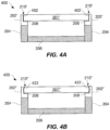
- FIGs. 4A and 4B are cross-sectional views of electronic device housings according to other embodiments that are similar to the electronic device housing 200 illustrated in FIG. 2A but which have different edge geometries for the outer device housing.
- FIG. 4A is a cross-sectional view of an electronic device housing 400 according to one embodiment.
- the electronic device housing 400 is the same as the electronic device housing 200 illustrated in FIG. 2A except that the edges 402 of the outer housing member 401' have been chamfered (or flattened).
- the protective side member 202' is molded against the edges of the outer housing member 401', including the chamfered edges 402.
- the outer exposed interface 210' between the sides (e.g., edges 402) of the outer housing member 201' and the peripheral side member 202' is essentially gap-free even though the edges 402 of the protective side member 202' are chamfered.
- FIG. 4B is a cross-sectional view of an electronic device housing 420 according to one embodiment.
- the electronic device housing 420 is the same as the electronic device housing 200 illustrated in FIG. 2A except that the edges 422 of the outer housing member 401" have been rounded.
- the protective side member 202" is molded against the edges of the outer housing member 401 ", including the rounded edges 422.
- the outer exposed interface 210" between the sides (e.g., edges 422) of the outer housing member 201" and the peripheral side member 202" is essentially gap-free even though the edges 422 of the protective side member 202" are rounded.
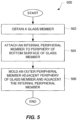
- FIG. 5 is a flow diagram of a housing formation process 500 according to one embodiment.
- the housing formation process 500 can operate to produce a housing for an electronic device, or at least a portion of such a housing.
- the housing formation process 500 can initially obtain 502 a glass member to be utilized with the housing for the electric device.
- the glass member to be utilized is a significant outer surface for the housing.
- the glass member can correspond to a top surface for the housing.
- the glass member can correspond to a bottom surface for the housing.
- the glass member is typically thin, particularly when the housing being formed is for a portable electronic device.
- the glass member has a thickness of less than 5 mm, and in another embodiment, the glass member has a thickness of less than 1 mm.
- an internal peripheral member can be attached 504 to the periphery of a bottom surface of the glass member.
- the internal peripheral member is attached 504 to the bottom surface of the glass member using an adhesive, though other means can be used, such as mechanical features (e.g., undercuts or interlocks).
- an outer peripheral member can be formed 506, e.g., molded, adjacent the periphery of the glass member and adjacent the inner peripheral member.
- the outer peripheral member provides an exposed outer surface for the housing.
- the outer peripheral member provides a thin protective later of material tightly adjacent the periphery of the glass member.
- the outer peripheral member can chemically bond with the inner peripheral member.
- the inner peripheral member and/or the outer peripheral member can be secured to a support structure for the housing so that the glass member is able to be mechanically secured to the housing.
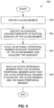
- FIG. 6 a flow diagram of a housing formation process 600 according to one embodiment.
- the housing formation process 600 can operate to produce a housing for an electronic device, or at least a portion of such a housing.
- the housing formation process 600 can initially obtain 602 a glass member.
- the glass member is to serve as a significant outer surface for the housing.
- the glass member can correspond to a top surface for the housing.
- the glass member can correspond to a bottom surface for the housing.
- the glass member is typically thin, particularly when used with portable electronic devices. In one embodiment, the glass member has a thickness of less than 5 mm, or more particularly less than 1 mm.
- an adhesive can be deposited 604 around a periphery of a bottom surface of the glass member.
- the glass member has a top surface that can represent an outer surface for the housing, and a bottom surface that is an inner surface that is not exposed.
- the adhesive being deposited 604 can be a thermally activated adhesive.
- the manner by which the adhesive is deposited can vary.
- the adhesive can be deposited 604 by forming a ring-like pattern of adhesive that can be placed around the periphery of the bottom surface of the glass member.
- the adhesive can be screen printed onto the periphery of the bottom surface of the glass member.
- an internal peripheral member can be placed 606 to the periphery of the glass member and adjacent the adhesive.
- the internal peripheral member can be secured to the bottom surface of the glass member using an adhesive, though other means can be used, such as mechanical features (e.g., undercuts or interlocks).
- the internal peripheral member can also be placed 606 by molding the internal peripheral member in place. In one embodiment, if the adhesive is thermally activated, the molding can also serve to activate the thermally activated adhesive so that a strong bond can be provided to the glass member and the internal peripheral member.
- an outer peripheral member can be molded 608 over the internal peripheral member such that the outer peripheral member is formed adjacent the periphery of the glass member and adjacent the inner peripheral member.
- the outer peripheral member provides an exposed outer surface for the housing.
- the outer peripheral member provides a thin protective later of material tightly adjacent the periphery of the glass member.
- the outer peripheral member can chemically bond with the inner peripheral member.
- a thermally activated adhesive could be used between the internal peripheral member and the outer peripheral member (or between the glass member and the outer peripheral member), and the molding of the outer peripheral member in place can also serve to activate the thermally activated adhesive so that a strong bond can be provided the inner peripheral member (and/or the glass member).
- the inner peripheral member and/or the outer peripheral member can be secured to a support structure for the housing so that the glass member is able to be mechanically secured to the housing.
- the peripheral members could be secured to the support structure by chemical bonding and/or mechanical features (e.g., undercuts or interlocks).
- FIG. 7A is a cross-sectional view of an electronic device housing 700 according to another embodiment.
- the electronic device housing 700 includes an outer housing member 701 supported and protected by an inner protective side member 702 and an outer protective side member 703.
- the inner protective side member 702 being positioned tightly adjacent sides of the outer housing member 701.
- the inner protective side member 702 can provide a thin layer of material positioned tightly adjacent sides of the outer housing member 701, thereby buffering impact at the sides of the outer housing member 701.
- the outer protective side member 703 being positioned tightly adjacent the sides of the inner protective side member 702 as well as the sides of the outer housing member 701.
- the outer and inner protective side members 702, 703 can individually or in combination provide a thin layer of material positioned tightly adjacent sides of the outer housing member 701, thereby buffering impact at the sides of the outer housing member 701.
- One or both of the inner and outer protective side members 702, 703 can also support the outer housing member 701 and serve to secure the outer housing member 701 to other portions of the electronic device housing 700.
- the outer protective side member 703 (and possibly also the inner protective side member 702) extends around all sides of the outer housing member 701. In another embodiment, the outer protective side member 703 (and possibly also the inner protective side member 702) extends around those of the sides of the outer housing member 701 that would otherwise be exposed.
- the outer housing member 701 can be secured to a support structure 704 of the electronic device housing 700.
- the support structure 704 can, for example, be an outer periphery member for the electronic device housing 700.
- the support structure 704 can couple to another outer housing member 706, which can be formed differently than the outer housing member 701.
- the inner protective side member 702 can be secured tightly adjacent the sides of the outer housing member 701 using an adhesive 708.
- the adhesive 708 can be applied as a layer of adhesive that is provided around a periphery of an inner side of the outer housing member 701. The adhesive 708 can thus serve to secure the inner protective side member 702 against the sides of the outer housing member 701.
- the outer protective side member 703 can be molded in place around at least a portion of the inner protective side member 702 as adjacent at least a portion of the sides of the outer housing member 701 so as to be tightly adjacent the sides of the outer housing member 701.
- the outer exposed interface 710 between the sides (e.g., edges) of the outer housing member 701 and the outer peripheral side member 703 is essentially gap-free.
- the outer protective side member 702 can be chemically bonded to at least a portion of the inner protective side member 702.
- the molding of the outer protective side member 703 can also serve to activate the thermally activated adhesive 708 so that a strong bond can be provided to the outer housing member 701 and the inner peripheral protective side member 702 via the adhesive 708.
- An internal space 712 is provided internal to the electronic device housing 700 whereby various electrical components can be attached, affixed or placed so as to provide electronic operations for the electronic device.
- the various members, parts or assemblies of the electronic device housing 700 can be formed of any of a variety of materials, e.g., glass, polymers or metal.
- the outer housing member 701 is glass
- the protective side members 702, 703 can be formed from a polymer (e.g., thermoplastic)
- the support structure 704 can be formed from metal or polymer (e.g., plastic)
- the another outer housing member 706 can be formed from glass, polymer (e.g., plastic) or metal.
- the protective side member 702 can be a structurally strengthened polymer (e.g., thermoplastic).
- the protective side member 702 can be polymer, such as polyarylamide, nylon or polycarbonate, which can be structurally strengthened by including glass fibers.
- some examples of some structurally strengthened polymers include 50% glass filled nylon and 30% glass filled polycarbonate.
- FIG. 7B is a cross-sectional assembly diagram for the electronic device housing 700 shown in FIG. 7A , according to one embodiment.
- the outer housing member 701 has a top surface 714 and a bottom surface 716.
- the bottom surface 716 of the outer housing member 701 has adhesive 708 applied as a layer of adhesive that is provided around a periphery of the bottom surface 716 of the outer housing member 701.
- the inner protective side member 702 can then be secured adjacent the sides of the outer housing member 701. More particularly, the inner protective side member 702 can be secured to the inner protective side member 702 using the adhesive 708 on the bottom surface 716 of the outer housing member 701.
- the outer protective side member 703 can be molded adjacent at least a portion of the sides of the outer housing member 701 and adjacent or over one or more sides of the inner protective side member 702. The molding process can also lead to chemical bonding of the outer protective side member 703 and the inner protective side member 702.
- the outer protective side member 703 can also be adjacent and secured to an upper side portion 718 of the support structure 704.
- the outer protective side member 703 is provided at the sides (i.e., edges) of the outer housing member 701, the outer protective side member 703 (alone or in combination with the inner protective side member 702) provides a buffer layer (e.g., bumper) that dampens impact induced at the sides of the outer housing member 701 of the electronic device housing 700.
- a buffer layer e.g., bumper
- FIG. 7C is a cross-sectional view of an electronic device housing 720 according to one embodiment.
- the electronic device housing 720 includes a first outer housing member 701 supported and protected by a first inner protective side member 702 and a first outer protective side member.
- the first inner protective side member 702 is positioned tightly adjacent sides of the first outer housing member 701.
- the outer protective side member 703 being positioned tightly adjacent the sides of the first inner protective side member 702 as well as the sides of the first outer housing member 701.
- the first outer and inner protective side members 702, 703 can individually or in combination provide a thin layer of material positioned tightly adjacent sides of the first outer housing member 701, thereby buffering impact at the sides of the first outer housing member 701.
- first inner and outer protective side members 702, 703 can also support the first outer housing member 701 and serve to secure the first outer housing member 701 to other portions of the electronic device housing 720.
- first outer protective side member 703 (and possibly also the first inner protective side member 702) extends around all sides of the first outer housing member 701.
- first outer protective side member 703 (and possibly also the first inner protective side member 702) extends around those of the sides of the first outer housing member 701 that would otherwise be exposed.
- the first inner protective side member 702 can be secured tightly adjacent the sides of the first outer housing member 701 using an adhesive 708.
- the adhesive 708 can be applied as a layer of adhesive that is provided around a periphery of an inner side of the first outer housing member 701. The adhesive 708 can thus serve to secure the first inner protective side member 702 against the sides of the first outer housing member 701.
- the first outer protective side member 703 can be molded in place around at least a portion of the first inner protective side member 702 as adjacent at least a portion of the sides of the first outer housing member 701 so as to be tightly adjacent the sides of the outer housing member 701.
- the outer exposed interface 710 between the sides (e.g., edges) of the first outer housing member 701 and the first outer peripheral side member 703 is essentially gap-free.
- the first outer protective side member 703 can be chemically bonded to at least a portion of the first inner protective side member 702.
- the adhesive 708 is thermally activated
- the molding of the first outer protective side member 703 can also serve to activate the thermally activated adhesive 708 so that a strong bond can be provided to the first outer housing member 701 and the first inner peripheral protective side member 702 via the adhesive 708.
- the electronic device housing 720 can also include an internal structure 722 that is integral with or secured to the support structure 704.
- the internal structure 722 can be secured to an inner surface of the support structure 704 such that it is offset from front and back planar boundaries of the support structure 704 (which may be an outer periphery member). As shown in FIG. 7C , the internal structure 722 can be secured at the mid-point of the height of the support structure 704.
- a first internal space 724 is provided internal to the electronic device housing 720 whereby various electrical components can be attached, affixed or placed so as to provide electronic operations for the electronic device.
- the electronic device housing 720 can also include similar structures on an opposite side of the electronic device housing 720.
- the electronic device housing 720 can further include a second outer housing member 726 supported and protected by a second inner protective side member 728 and a second outer protective side member 729.
- the second inner protective side member 728 can be positioned tightly adjacent sides of the second outer housing member 726.
- the second outer protective side member 729 can be positioned tightly adjacent the sides of the inner protective side member 702 as well as the sides of the second outer housing member 726.
- the second outer and inner protective side members 728, 729 can individually or in combination provide a thin layer of material positioned tightly adjacent sides of the second outer housing member 726, thereby buffering impact at the sides of the second outer housing member 726.
- One or both of the second inner and outer protective side members 728, 729 can also support the second outer housing member 726 and serve to secure the second outer housing member 726 to other portions of the electronic device housing 720.
- the second outer protective side member 729 (and possibly also the inner protective side member 728) extends around all sides of the second outer housing member 726.
- the second outer protective side member 729 (and possibly also the second inner protective side member 728) extends around those of the sides of the second outer housing member 726 that would otherwise be exposed.
- the second inner protective side member 728 can be secured tightly adjacent the sides of the second outer housing member 726 using an adhesive 730.
- the adhesive 730 can be applied as a layer of adhesive that is provided around a periphery of an inner side of the second outer housing member 726. The adhesive 730 can thus serve to secure the second inner protective side member 728 against the sides of the second outer housing member 726.
- the second outer protective side member 729 can be molded in place around at least a portion of the second inner protective side member 728 and adjacent at least a portion of the sides of the second outer housing member 726 so as to be tightly adjacent the sides of the second outer housing member 726.
- the outer exposed interface 731 between the sides (e.g., edges) of the second outer housing member 726 and the second outer peripheral side member 729 is essentially gap-free.
- the second outer protective side member 729 can be chemically bonded to at least a portion of the second inner protective side member 728.
- the adhesive 730 is thermally activated
- the molding of the second outer protective side member 729 can also serve to activate the thermally activated adhesive 730 so that a strong bond can be provided to the second outer housing member 726 and the second inner peripheral protective side member 728 via the adhesive 730.
- An internal space 712 is provided internal to the electronic device housing 700 whereby various electrical components can be attached, affixed or placed so as to provide electronic operations for the electronic device.
- a second internal space 732 is provided internal to the electronic device housing 720 (between the internal structure 722 and the second outer housing member 726) whereby various electrical components can be attached, affixed or placed so as to provide electronic operations for the electronic device.
- the second internal space 732 can be separate from or joined with the first internal space 724.
- the various members, parts or assemblies of the electronic device housing 720 can be formed of any of a variety of materials, e.g., glass, polymers or metal.
- the outer housing members 701, 726 are glass
- the protective side members 702, 703, 728, 729 can be formed from a polymer (e.g., thermoplastic)
- the support structures 704, 722 can be formed from metal or polymer (e.g., plastic).
- the protective side members 702, 703, 728, 729 can be a structurally strengthened polymer (e.g., thermoplastic).
- the protective side members 702, 703, 728, 729 can be polymer, such as polyarylamide, nylon or polycarbonate, which can be structurally strengthened by including glass fibers.
- some examples of some structurally strengthened polymers include 50% glass filled nylon and 30% glass filled polycarbonate.
- first outer housing member 701 can represent a top outer surface for the portable electronic device
- second outer surface housing 726 can represent a bottom outer surface housing.
- both the first outer housing member 701 and the second outer housing member 726 are glass (e.g., glass covers).
- the protective side members discussed above are typically thin layers of material positioned tightly adjacent sides of the outer housing member, thereby buffering impact at the sides of the outer housing members.
- the protective side members are to be strong; hence, a structurally strengthened polymer, such as polyarylamide, can be utilized.
- the polyarylamide can be strengthened by containing glass fibers.
- IXEF polyarylamide PARA
- Solvay Advanced Polymers L.L.C which can contain glass fiber reinforcement.
- the protective side members are tightly adjacent sides of the outer housing member, the respective materials used for the protective side members and the outer housing member.
- the Coefficient of Thermal Expansion (CTE) of the respective materials can produce undesired stress on the sides of the outer housing member.
- CTE Coefficient of Thermal Expansion
- the CTE of the material for the protective side members would be about 10 millimeters/meter/°C.
- plastics tend to have CTE's (e.g., roughly 100 millimeters/meter/°C) that are dramatically higher than that of glass
- some manufactured polymers such as polyarylamide, can have CTE's (e.g., roughly 30 millimeters/meter/°C) that are substantially closer to that of glass and thereby would, if used, induce less stress on the sides of the outer housing member.
- a manufactured polymer for such use could have a CTE less than or equal to about 50 millimeters/meter/°C, and in another embodiment, a manufactured polymer for such use could have a CTE less than or equal to about 35 millimeters/meter/°C.
- additive can be added to a polymer so to bring is CTE closer to that of glass.
- the additives can be particles or fibers which can be formed from glass or ceramic.
- the thickness of the protective side member can be thin, for example, the thickness can be on the order of about 1 mm or less in one embodiment.
- the protective side materials can be formed from multiple materials that can be alternated, intertwined or layered.
- the later of material against the edges of the outer housing member of glass can have a CTE relatively close to that of glass while an outer layer can have a higher CTE can permit a greater range of material, such as polymers (e.g., plastics).
- the protective side members are able to be thin yet be cosmetically unintrusive.
- the thickness (t1) for the protective side member can be less than 1 mm (e.g., 0.8 mm).
- the thickness (t2) of the outer housing member can be less than 5 mm (e.g., 1 mm).
- these thicknesses are exemplary and vary with the size of the electronic device housing and with desired strength.
- Using a strengthened material for the protective side members as noted above can also be advantageous. Nevertheless, the provisioning of thin protective side members for outer housing members, such as glass covers, facilitates providing portable electronic device housings that are compact and thin yet resistant to side impact damage to the outer housing members.
- a glass member for which a component e.g., peripheral side member
- a component e.g., peripheral side member
- a metal mold is normally used in molding.
- the metal mold can damage (e.g., scratch) a glass member during molding.
- the metal mold i.e., its inner surfaces
- the coating can, for example, be a thin layer of polytetrafluoroethylene (PTFE) or polyimide film.
- An electronic device enclosure comprising: a glass cover for a top surface for the electronic device enclosure; an adhesive deposited around a periphery of the glass cover; and a peripheral structure for providing a support surface for the glass cover and for providing side protective surfaces for the glass cover, the peripheral structure being at least partially secured to the glass cover by the adhesive.
- peripheral structure comprises a polymer strengthened by containing glass fibers.
- peripheral structure comprises a polymer
- the polymer includes additives such that the CTE of the peripheral structure is made closer to the CTE of the glass cover.
- peripheral structure is molded about the periphery of the glass cover and molded adjacent the adhesive, and wherein the adhesive includes a feature to which the peripheral structure is formed.
- peripheral structure is molded about the periphery of the glass cover and molded adjacent the adhesive, and wherein the metal support has at least one feature that provides a mechanical interlock with the peripheral structure after the peripheral structure has been molded.
- peripheral structure includes an inner peripheral member and an outer peripheral member, wherein the inner peripheral member is attached to the glass cover via the adhesive, and wherein at least the outer peripheral member is molded about at least a portion of the periphery of the glass cover and about at least a portion of the inner peripheral member.
- a method for assembling an electronic device comprising: obtaining a glass member having a top surface and a bottom surface, the top surface providing an outer surface for substantially all of a surface of the electronic device; depositing an adhesive layer around a periphery of the bottom surface of the glass member; aligning the glass member relative to a support structure for the electronic device; and molding a peripheral protective side portion for the electronic device, the peripheral protective side portion being molded adjacent the periphery of the glass member, adjacent the adhesive layer, and adjacent the support structure.
- a method as recited in clause 19, wherein the depositing of the adhesive layer comprises: screen printing the adhesive layer to the periphery of the bottom surface of the glass member.
- a method as recited in clause 19, wherein the depositing of the adhesive layer comprises: placing an adhesive film on at least a portion of the bottom surface of the glass member.
- a method for assembling an electronic device comprising: obtaining a glass member having a top surface and a bottom surface, the top surface providing an outer surface for substantially all of a surface of the electronic device; attaching an internal periphery member to a periphery of the bottom surface of the glass member; and molding an outer periphery member adjacent a periphery of the glass member and adjacent the internal periphery member.
- said molding comprises: obtaining a metal mold having an inner surface configured to form the outer periphery member for the electronic device; coating at least a portion of the inner surface of the metal mold; and injecting a molding material into the metal mold to form the outer periphery member for the electronic device.
Abstract
Description
- Conventionally, a portable electronic device has a housing that encases the various electrical components of the portable electronic device. Often, the portable electronic device has a display arrangement that includes various layers. The various layers usually include at least a display technology layer, and may additionally include a sensing arrangement (e.g., touch sensors or touch screen) and/or a cover window disposed over the display technology layer. The cover window can be a plastic or glass cover that provides a protective outer surface that protects the display technology layer. The cover window can form part of an outer surface for the housing of the portable electronic device. Conventionally, supporting or securing the cover window to other portions of the housing tends to impede usage of a peripheral area of the cover window.
- Unfortunately, however, as portable electronic device continue to be made smaller, thinner and/or more powerful, there remains a continuing need to provide improved techniques and structures for supporting cover windows of portable electronic device housings.
- The invention pertains to an electronic device having an enclosure formed from at least one glass cover and a peripheral structure formed adjacent the periphery of the glass cover. The peripheral structure can be secured adjacent to the glass cover with an adhesive. The peripheral structure can be molded adjacent the glass cover so that a gapless interface is formed between the peripheral structure and the periphery of the glass cover. In one embodiment, the peripheral structure can include at least an inner peripheral structure and an outer peripheral structure. The enclosure for the electronic device is can be thin yet be sufficiently strong to be suitable for use in electronic devices, such as portable electronic devices.
- The invention can be implemented in numerous ways, including as a method, system, device, or apparatus. Several embodiments of the invention are discussed below.
- As an electronic device enclosure, one embodiment can, for example, include at least a glass cover for a top surface for the electronic device enclosure, an adhesive deposited around a periphery of the glass cover, and a peripheral structure for providing a support surface for the glass cover and for providing side protective surfaces for the glass cover. The peripheral structure is at least partially secured to the glass cover by the adhesive.
- As a method for assembling an electronic device, one embodiment of the method can, for example, include at least: obtaining a glass member having a top surface and a bottom surface, the top surface providing an outer surface for substantially all of a surface of the electronic device; depositing an adhesive layer around a periphery of the bottom surface of the glass member; aligning the glass member relative to a support structure for the electronic device; and molding a peripheral protective side portion for the electronic device, the peripheral protective side portion being molded adjacent the periphery of the glass member, adjacent the adhesive layer, and adjacent the support structure.
- As a method for assembling an electronic device, one embodiment of the method can, for example, include at least: obtaining a glass member having a top surface and a bottom surface, the top surface providing an outer surface for substantially all of a surface of the electronic device; attaching an internal periphery member to a periphery of the bottom surface of the glass member; and molding an outer periphery member adjacent a periphery of the glass member and adjacent the internal periphery member.
- As a method for assembling an electronic device, one embodiment of the method can, for example, include at least: obtaining a glass member having a top surface and a bottom surface, the top surface providing an outer surface for substantially all of a surface of the electronic device; providing an adhesive layer around a periphery of the bottom surface of the glass member; and molding a peripheral protective side portion for the electronic device. The peripheral protective side portion being molded adjacent the periphery of the glass member and being secured to the glass member via the adhesive layer.
- Other aspects and advantages of the invention will become apparent from the following detailed description taken in conjunction with the accompanying drawings which illustrate, by way of example, the principles of the invention.
- The invention will be readily understood by the following detailed description in conjunction with the accompanying drawings, wherein like reference numerals designate like structural elements, and in which:
-
FIG. 1 is a flow diagram of a housing formation process according to one embodiment of the invention. -
FIG. 2A is a cross-sectional view of an electronic device housing according to one embodiment. -
FIG. 2B is a cross-sectional assembly diagram for the electronic device housing shown inFIG. 2A , according to one embodiment. -
FIG. 2C is a cross-sectional view of an electronic device housing according to one embodiment. -
FIG. 3A is a cross-sectional view of an electronic device housing according to one embodiment. -
FIG. 3B is a cross-sectional assembly diagram for the electronic device housing shown inFIG. 3A , according to one embodiment. -
FIG. 3C is a cross-sectional view of an electronic device housing according to one embodiment. -
FIG. 4A is a cross-sectional view of an electronic device housing according to one embodiment. -
FIG. 4B is a cross-sectional view of an electronic device housing according to one embodiment. -
FIG. 5 is a flow diagram of a housing formation process according to one embodiment. -
FIG. 6 a flow diagram of a housing formation process according to one embodiment. -
FIG. 7A is a cross-sectional view of an electronic device housing according to another embodiment. -
FIG. 7B is a cross-sectional assembly diagram for the electronic device housing shown inFIG. 7A , according to one embodiment. -
FIG. 7C is a cross-sectional view of an electronic device housing according to one embodiment. - Embodiments are described herein in the context of a housing for an electronic device. The housing can make use of an outer member, which can be formed of glass. The outer member can be aligned, protected and/or secured with respect to other portions of the housing for the electronic device. The electronic device can be portable and in some cases handheld.
- According to one aspect, the invention pertains to an electronic device having an enclosure formed from at least one glass cover and a peripheral structure formed adjacent the periphery of the glass cover. The peripheral structure can be secured adjacent to the glass cover with an adhesive. The peripheral structure can be molded adjacent the glass cover so that a gapless interface is formed between the peripheral structure and the periphery of the glass cover. In one embodiment, the peripheral structure includes at least an inner peripheral structure and an outer peripheral structure.
- The following detailed description is illustrative only, and is not intended to be in any way limiting. Other embodiments will readily suggest themselves to skilled persons having the benefit of this disclosure. Reference will now be made in detail to implementations as illustrated in the accompanying drawings. The same reference indicators will generally be used throughout the drawings and the following detailed description to refer to the same or like parts. It should be appreciated that the drawings are generally not drawn to scale, and at least some features of the drawings have been exaggerated for ease of illustration.
- In the interest of clarity, not all of the routine features of the implementations described herein are shown and described. It will, of course, be appreciated that in the development of any such actual implementation, numerous implementation-specific decisions must be made in order to achieve the developer's specific goals, such as compliance with application and business related constraints, and that these specific goals will vary from one implementation to another and from one developer to another. Moreover, it will be appreciated that such a development effort might be complex and time-consuming, but would nevertheless be a routine undertaking of engineering for those of ordinary skill in the art having the benefit of this disclosure.
- Embodiments of the invention can relate to apparatus, systems and methods for forming a housing having a thin glass member for an electronic device. In one example, the glass member may be an outer surface of an electronic device. The glass member may for example correspond to a glass cover that helps form part of a display area of an electronic device (i.e., situated in front of a display either as a separate part or integrated within the display. Alternatively or additionally, the glass member may form a part of the housing. For example, it may form an outer surface other than in the display area.
- The apparatus, systems and methods for improving strength of thin glass are especially suitable for glass covers, or displays (e.g., LCD displays), assembled in small form factor electronic devices such as handheld electronic devices (e.g., mobile phones, media players, personal digital assistants, remote controls, etc.). The glass can be thin in these small form factor embodiments, such as less than 3 mm, or more particularly between 0.5 and 2.5 mm, or even more particularly between 0.3 and 1.0 mm. The apparatus, systems and methods can also be used for glass covers or displays for other devices including, but not limited to including, relatively larger form factor electronic devices (e.g., portable computers, tablet computers, displays, monitors, televisions, etc.). The glass can also be thin in these larger form factor embodiments, such as less than 5 mm, or more particularly between 0.5 and 3 mm, or even more particularly between 0.3 and 2.0 mm.
- Embodiments are discussed below with reference to
FIGs. 1 - 7C . However, those skilled in the art will readily appreciate that the detailed description given herein with respect to these figures is for explanatory purposes as the invention extends beyond these limited embodiments. -
FIG. 1 a flow diagram of ahousing formation process 100 according to one embodiment of the invention. Thehousing formation process 100 can operate to produce a housing for an electronic device, or at least a portion of such a housing. - The
housing formation process 100 can initially obtain 102 a glass member. The glass member is to serve as a significant outer surface for the housing. For example, the glass member can correspond to a top surface for the housing. Alternatively or additionally, the glass member can correspond to a bottom surface for the housing. The glass member is typically thin, particularly when used with portable electronic devices. In one embodiment, the glass member has a thickness of less than 5 mm, or more particularly less than 1 mm. - After the glass member has been obtained 102, an adhesive can be deposited 104 around a periphery of a bottom surface of the glass member. The glass member has a top surface that can represent an outer surface for the housing, and a bottom surface that is an inner surface that is not exposed. In one embodiment, the adhesive being deposited 104 can be a thermally activated adhesive. The adhesive can, for example, by provided as film or as a layer. Also, the manner by which the adhesive is deposited can vary. In one implementation, the adhesive can be deposited 104 by forming a ring-like pattern of adhesive that can be placed around the periphery of the bottom surface of the glass member. In another implementation, the adhesive can be screen printed onto the periphery of the bottom surface of the glass member.
- Thereafter, the glass member can be aligned 106 relative to a support structure. The support structure can be provided as being a component of the housing for the electronic device. For example, the support can pertain to a side structure for the housing or an interior support member. After the glass member has been aligned 106 with the support structure, a peripheral protective side portion can be molded 108 adjacent to the periphery of the glass member and adjacent to the adhesive. The adhesive can serve to secure the peripheral protective side member to the glass member. The peripheral protective side member being molded 108 can also be formed adjacent the support structure. Typically, the peripheral side portion would also be secured to the support structure by chemical bonding and/or mechanical features (e.g., undercuts or interlocks). In such case, the glass member and the peripheral protective side member are secured to the support structure and thus form at least a portion of the housing for the electronic device. Also, if the adhesive is thermally activated, the
molding 108 can also serve to activate the thermally activated adhesive so that a strong bond can be provided to the glass member and the peripheral protective side manner. -
FIG. 2A is a cross-sectional view of anelectronic device housing 200 according to one embodiment. Theelectronic device housing 200 includes anouter housing member 201 supported and protected by aprotective side member 202. Theprotective side member 202 being positioned tightly adjacent sides of theouter housing member 201. Theprotective side members 202 can provide a thin layer of material positioned tightly adjacent sides of theouter housing member 201, thereby buffering impact at the sides of theouter housing member 201. Theprotective side member 202 also supports theouter housing member 201 and serves to secure theouter housing member 201 to other portions of theelectronic device housing 200. In one embodiment, theprotective side member 202 extends around all sides of theouter housing member 201. In another embodiment, theprotective side member 202 extends around those of the sides of theouter housing member 201 that would otherwise be exposed. - As shown in
FIG. 2A , theouter housing member 201 can be secured to asupport structure 204 of theelectronic device housing 200. Thesupport structure 204 can, for example, be an outer periphery member for theelectronic device housing 200. In one embodiment, thesupport structure 204 can couple to anotherouter housing member 206, which can be formed differently than theouter housing member 201. - The
protective side member 202 can be secured tightly adjacent the sides of theouter housing member 201 using an adhesive 208. In one embodiment, the adhesive 208 can be applied as a layer of adhesive that is provided around a periphery of an inner side of theouter housing member 201. Theprotective side member 202 can also be molded in place so as to be tightly adjacent the sides of theouter housing member 201. By molding theprotective side member 202 in place, the outer exposedinterface 210 between the sides (e.g., edges) of theouter housing member 201 and theperipheral side member 202 is essentially gap-free. Theprotective side member 202 can also be molded against the adhesive 208 deposited on the periphery of the bottom side of theouter housing member 201. The adhesive 208 can thus serve to secure theprotective side member 202 against the sides of theouter housing member 201. Also, if the adhesive 208 is thermally activated, the molding of theprotective side member 202 can also serve to activate the thermally activated adhesive 208 so that a strong bond can be provided to theouter housing member 201 and the peripheralprotective side member 202 via the adhesive 208. Aninternal space 212 is provided internal to theelectronic device housing 200 whereby various electrical components can be attached, affixed or placed so as to provide electronic operations for the electronic device. - The various members, parts or assemblies of the
electronic device housing 200 can be formed of any of a variety of materials, e.g., glass, polymers or metal. In one embodiment, theouter housing member 201 is glass, theprotective side member 202 is be formed from polymer (e.g., thermoplastic), thesupport structure 204 is formed from metal or polymer (e.g., plastic), and the anotherouter housing member 206 is formed from glass, polymer (e.g., plastic) or metal. More particularly, in some embodiments, theprotective side member 202 can be a structurally strengthened polymer (e.g., thermoplastic). As an example, theprotective side member 202 can be polymer, such as polyarylamide, nylon or polycarbonate, which can be structurally strengthened by including glass fibers. For example, some examples of some structurally strengthened polymers include 50% glass filled nylon and 30% glass filled polycarbonate. -
FIG. 2B is a cross-sectional assembly diagram for theelectronic device housing 200 shown inFIG. 2A , according to one embodiment. Theouter housing member 201 has a top surface 214 and a bottom surface 216. The bottom surface 216 of theouter housing member 201 has adhesive 208 applied as a layer of adhesive that is provided around a periphery of the bottom surface 216 of theouter housing member 201. Theprotective side member 202 can then be molded adjacent the sides of theouter housing member 201. When theprotective side member 202 is molded, theprotective side member 202 is also at least partially formed adjacent the adhesive 208 on the bottom surface 216 of the outer housing member. Moreover, when theprotective side member 202 is formed, theprotective side member 202 can also be adjacent and secured to an upper side portion 218 of thesupport structure 204. When theprotective side member 202 are provided at the sides (i.e., edges) of theouter housing member 201, theprotective side member 202 provides a buffer layer (e.g., bumper) that dampens impact induced at the sides of theouter housing member 201 of theelectronic device housing 200. -
FIG. 2C is a cross-sectional view of anelectronic device housing 220 according to one embodiment. Theelectronic device housing 220 includes a firstouter housing member 201 supported and protected by a firstprotective side member 202. The firstprotective side member 202 is positioned tightly adjacent sides of the firstouter housing member 201. The firstprotective side member 202 also supports the firstouter housing member 201 and serves to secure the firstouter housing member 201 to other portions of theelectronic device housing 220. In this embodiment, the firstprotective side member 202 is secured to not only the firstouter housing member 201 but also asupport structure 204. Thesupport structure 204 may be an outer periphery member for theelectronic device housing 220. - The first
protective side member 202 can be secured tightly adjacent the sides of theouter housing member 201 using the adhesive 208. In one embodiment, the adhesive 208 can be applied as a layer of adhesive that is provided around a periphery of an inner side of the firstouter housing member 201. The firstprotective side member 202 can also be molded in place so as to be tightly adjacent the sides of the firstouter housing member 201. By molding the firstprotective side member 202 in place, the outer exposedinterface 210 between the sides (e.g., edges) of theouter housing member 201 and theperipheral side member 202 is essentially gap-free. The firstprotective side member 202 can also be molded against the adhesive 208 deposited on the periphery of the bottom side of the firstouter housing member 201. The adhesive 208 can thus serve to secure the firstprotective side member 202 against the sides of theouter housing member 201. Also, if the adhesive 208 is thermally activated, the molding of the firstprotective side member 202 can also serve to activate the thermally activated adhesive 208 so that a strong bond can be provided to the firstouter housing member 201 and the first peripheralprotective side member 202 via the adhesive 208. - The
electronic device housing 220 can also include aninternal structure 222 that is integral with or secured to thesupport structure 204. In one embodiment, theinternal structure 222 can be secured to an inner surface of thesupport structure 204 such that it is offset from front and back planar boundaries of the support structure 204 (which may be an outer periphery member). As shown inFIG. 2C , theinternal structure 222 can be secured at the mid-point of the height of thesupport structure 204. A firstinternal space 224 is provided internal to theelectronic device housing 220 whereby various electrical components can be attached, affixed or placed so as to provide electronic operations for the electronic device. - In this embodiment, the
electronic device housing 220 can also include similar structures on an opposite side of theelectronic device housing 220. Namely, theelectronic device housing 220 can further include a secondouter housing member 226 supported and protected by a secondprotective side member 228. The secondprotective side member 228 can be positioned tightly adjacent sides of the secondouter housing member 226. The secondprotective side member 228 also supports the secondouter housing member 226 and serves to secure the secondouter housing member 226 to other portions of theelectronic device housing 220. In this embodiment, the secondprotective side member 228 is secured to not only the secondouter housing member 226 but also thesupport structure 204. As previously noted, thesupport structure 204 may be an outer periphery member for theelectronic device housing 220. In this embodiment, the secondprotective side member 228 can be secured to theouter periphery member 204 on the opposite side from the firstprotective side member 202. The secondprotective side member 228 can be secured tightly adjacent the sides of the secondouter housing member 226 using an adhesive 330. In one embodiment, the adhesive 330 can be applied as a layer of adhesive that is provided around a periphery of an inner side of the secondouter housing member 226. The secondprotective side member 228 can also be molded in place so as to be tightly adjacent the sides of the secondouter housing member 226. Further, a secondinternal space 232 is provided internal to the electronic device housing 220 (between theinternal structure 222 and the second outer housing member 226) whereby various electrical components can be attached, affixed or placed so as to provide electronic operations for the electronic device. The second internal space 230 can be separate from or joined with the firstinternal space 224. - In one embodiment, the first
outer housing member 201 can represent a top outer surface for the portable electronic device, and the secondouter surface housing 226 can represent a bottom outer surface housing. In one embodiment, both the firstouter housing member 201 and the secondouter housing member 226 are glass (e.g., glass covers). -
FIG. 3A is a cross-sectional view of anelectronic device housing 300 according to one embodiment. Theelectronic device housing 300 includes anouter housing member 301 supported and protected by aprotective side member 302. Theprotective side member 302 being positioned tightly adjacent sides of theouter housing member 301. Theprotective side members 302 can provide a thin layer of material positioned tightly adjacent sides of theouter housing member 301, thereby buffering impact at the sides of theouter housing member 301. Theprotective side member 302 also supports theouter housing member 301 and serves to secure theouter housing member 301 to other portions of theelectronic device housing 300. In one embodiment, theprotective side member 302 extends around all sides of theouter housing member 301. In another embodiment, theprotective side member 302 extends around those of the sides of theouter housing member 301 that would otherwise be exposed. - As shown in
FIG. 3A , theouter housing member 301 can be secured to asupport structure 304 of theelectronic device housing 300. In one embodiment, as shown inFIG. 3A , one or more securing features 305 can be provided on an upper surface of thehousing structure 304. The securing features 305 can be integral with thehousing structure 304. The securing features 305 (e.g., mechanical features, such as undercuts or interlocks) can be used to assist with the securing of the protective side member 302 (and thus the outer housing member 301) to thehousing structure 304. Thesupport structure 304 can, for example, be an outer periphery member for theelectronic device housing 300. Thesupport structure 304 can couple to anotherouter housing member 306, which can be formed differently than theouter housing member 301. - The
protective side member 302 can be secured tightly adjacent the sides of theouter housing member 301 using an adhesive 308. In one embodiment, the adhesive 308 can be applied as a layer of adhesive that is provided around a periphery of an inner side of theouter housing member 301. Theprotective side member 302 can also be molded in place so as to be tightly adjacent the sides of theouter housing member 301. By molding theprotective side member 302 in place, the outer exposedinterface 310 between the sides (e.g., edges) of theouter housing member 301 and theperipheral side member 302 is essentially gap-free. Theprotective side member 302 can also be molded against the adhesive 308 deposited on the periphery of the bottom side of theouter housing member 301. The adhesive 308 can thus serve to secure theprotective side member 302 against the sides of theouter housing member 301. Also, if the adhesive 308 is thermally activated, the molding of theprotective side member 302 can also serve to activate the thermally activated adhesive 308 so that a strong bond can be provided to theouter housing member 301 and the peripheralprotective side member 302 via the adhesive 308. Aninternal space 312 is provided internal to theelectronic device housing 300 whereby various electrical components can be attached, affixed or placed so as to provide electronic operations for the electronic device. - The various members, parts or assemblies of the
electronic device housing 300 can be formed of any of a variety of materials, e.g., glass, polymers or metal. In one embodiment, theouter housing member 301 is glass, theprotective side member 302 is be formed from polymer (e.g., thermoplastic), thesupport structure 304 is formed from metal or polymer (e.g., plastic), and the anotherouter housing member 306 is formed from glass, polymer (e.g., plastic) or metal. More particularly, in some embodiments, theprotective side member 302 can be a structurally strengthened polymer (e.g., thermoplastic). As an example, theprotective side member 302 can be polymer, such as polyarylamide, nylon or polycarbonate, which can be structurally strengthened by including glass fibers. For example, some examples of some structurally strengthened polymers include 50% glass filled nylon and 30% glass filled polycarbonate. -
FIG. 3B is a cross-sectional assembly diagram for theelectronic device housing 300 shown inFIG. 3A , according to one embodiment. Theouter housing member 301 has a top surface 314 and abottom surface 316. Thebottom surface 316 of theouter housing member 301 has adhesive 308 applied as a layer of adhesive that is provided around a periphery of thebottom surface 316 of theouter housing member 301. Theprotective side member 302 can then be molded adjacent the sides of theouter housing member 301. When theprotective side member 302 is molded, theprotective side member 302 is also at least partially formed adjacent the adhesive 308 on thebottom surface 316 of the outer housing member. Moreover, when theprotective side member 302 is formed, theprotective side member 302 can also be adjacent and secured to an upper side portion 318 of thesupport structure 304. In one embodiment, as shown inFIG. 3B , one or more securing features 305 can be provided on an upper surface of thehousing structure 304. Theprotective side member 302 can be also molded around the one or more securing features 305, which can further secure theprotective side member 302 to thesupport structure 304. When theprotective side member 302 are provided at the sides (i.e., edges) of theouter housing member 301, theprotective side member 302 provides a buffer layer (e.g., bumper) that dampens impact induced at the sides of theouter housing member 301 of theelectronic device housing 300. -
FIG. 3C is a cross-sectional view of anelectronic device housing 320 according to one embodiment. Theelectronic device housing 320 includes a firstouter housing member 301 supported and protected by a firstprotective side member 302. The firstprotective side member 302 is positioned tightly adjacent sides of the firstouter housing member 301. The firstprotective side member 302 also supports the firstouter housing member 301 and serves to secure the firstouter housing member 301 to other portions of theelectronic device housing 320. In this embodiment, the firstprotective side member 302 is secured to not only the firstouter housing member 301 but also asupport structure 304. In addition, in this embodiment, one or more securing features 305 can be provided on an upper surface of thehousing structure 304. Thesupport structure 304 may be an outer periphery member for theelectronic device housing 320. - The first
protective side member 302 can be secured tightly adjacent the sides of theouter housing member 301 using the adhesive 308. In one embodiment, the adhesive 308 can be applied as a layer of adhesive that is provided around a periphery of an inner side of the firstouter housing member 301. The firstprotective side member 302 can also be molded in place so as to be tightly adjacent the sides of the firstouter housing member 301. By molding the firstprotective side member 302 in place, the outer exposedinterface 310 between the sides (e.g., edges) of theouter housing member 301 and theperipheral side member 302 is essentially gap-free. The firstprotective side member 302 can also be molded against the adhesive 308 deposited on the periphery of the bottom side of the firstouter housing member 301. The adhesive 308 can thus serve to secure the firstprotective side member 302 against the sides of theouter housing member 301. Also, if the adhesive 308 is thermally activated, the molding of the firstprotective side member 302 can also serve to activate the thermally activated adhesive 308 so that a strong bond can be provided to the firstouter housing member 301 and the first peripheralprotective side member 302 via the adhesive 308. - The
electronic device housing 320 can also include an internal structure 322 that is integral with or secured to thesupport structure 304. In one embodiment, the internal structure 322 can be secured to an inner surface of thesupport structure 304 such that it is offset from front and back planar boundaries of the support structure 304 (which may be an outer periphery member). As shown inFIG. 3C , the internal structure 322 can be secured at the mid-point of the height of thesupport structure 304. A firstinternal space 324 is provided internal to theelectronic device housing 320 whereby various electrical components can be attached, affixed or placed so as to provide electronic operations for the electronic device. - In this embodiment, the
electronic device housing 320 can also include similar structures on an opposite side of theelectronic device housing 320. Namely, theelectronic device housing 320 can further include a secondouter housing member 326 supported and protected by a secondprotective side member 328. The secondprotective side member 328 can be positioned tightly adjacent sides of the secondouter housing member 326. The secondprotective side member 328 also supports the secondouter housing member 326 and serves to secure the secondouter housing member 326 to other portions of theelectronic device housing 320. In this embodiment, the secondprotective side member 328 is secured to not only the secondouter housing member 326 but also thesupport structure 304. In addition, in this embodiment, one or more securing features 329 can be provided on a bottom surface of thehousing structure 304. The securing features 329 can be integral with thehousing structure 304. As previously noted, thesupport structure 304 may be an outer periphery member for theelectronic device housing 320. In this embodiment, the secondprotective side member 328 can be secured to theouter periphery member 304 on the opposite side from the firstprotective side member 302. The secondprotective side member 328 can be secured tightly adjacent the sides of the secondouter housing member 326 using an adhesive 330. In one embodiment, the adhesive 330 can be applied as a layer of adhesive that is provided around a periphery of an inner side of the secondouter housing member 326. The secondprotective side member 328 can also be molded in place so as to be tightly adjacent the sides of the secondouter housing member 326. Further, a secondinternal space 332 is provided internal to the electronic device housing 320 (between the internal structure 322 and the second outer housing member 326) whereby various electrical components can be attached, affixed or placed so as to provide electronic operations for the electronic device. The secondinternal space 330 can be separate from or joined with the firstinternal space 324. - In one embodiment, the first
outer housing member 301 can represent a top outer surface for the portable electronic device, and the secondouter surface housing 326 can represent a bottom outer surface housing. In one embodiment, both the firstouter housing member 301 and the secondouter housing member 326 are glass (e.g., glass covers). - Although the edges of the outer housing members (201, 226, 301, 326) can be square as suggested by
FIGs. 2A-3C , it should understood that the edges of the outer housing member need not be square but can be formed with other geometries, such as with chamfered (or flattened) edges or rounded edges.FIGs. 4A and 4B are cross-sectional views of electronic device housings according to other embodiments that are similar to theelectronic device housing 200 illustrated inFIG. 2A but which have different edge geometries for the outer device housing. -
FIG. 4A is a cross-sectional view of anelectronic device housing 400 according to one embodiment. Theelectronic device housing 400 is the same as theelectronic device housing 200 illustrated inFIG. 2A except that theedges 402 of the outer housing member 401' have been chamfered (or flattened). Additionally, the protective side member 202' is molded against the edges of the outer housing member 401', including the chamfered edges 402. Hence, as with other embodiments, by molding the protective side member 202' in place, the outer exposed interface 210' between the sides (e.g., edges 402) of the outer housing member 201' and the peripheral side member 202' is essentially gap-free even though theedges 402 of the protective side member 202' are chamfered. -
FIG. 4B is a cross-sectional view of anelectronic device housing 420 according to one embodiment. Theelectronic device housing 420 is the same as theelectronic device housing 200 illustrated inFIG. 2A except that theedges 422 of the outer housing member 401" have been rounded. Additionally, theprotective side member 202" is molded against the edges of the outer housing member 401 ", including the rounded edges 422. Hence, as with other embodiments, by molding theprotective side member 202" in place, the outer exposedinterface 210" between the sides (e.g., edges 422) of theouter housing member 201" and theperipheral side member 202" is essentially gap-free even though theedges 422 of theprotective side member 202" are rounded. -
FIG. 5 is a flow diagram of ahousing formation process 500 according to one embodiment. Thehousing formation process 500 can operate to produce a housing for an electronic device, or at least a portion of such a housing. - The
housing formation process 500 can initially obtain 502 a glass member to be utilized with the housing for the electric device. The glass member to be utilized is a significant outer surface for the housing. For example, the glass member can correspond to a top surface for the housing. Alternatively, the glass member can correspond to a bottom surface for the housing. The glass member is typically thin, particularly when the housing being formed is for a portable electronic device. In one embodiment, the glass member has a thickness of less than 5 mm, and in another embodiment, the glass member has a thickness of less than 1 mm. - Next, an internal peripheral member can be attached 504 to the periphery of a bottom surface of the glass member. Typically, the internal peripheral member is attached 504 to the bottom surface of the glass member using an adhesive, though other means can be used, such as mechanical features (e.g., undercuts or interlocks).
- Thereafter, an outer peripheral member can be formed 506, e.g., molded, adjacent the periphery of the glass member and adjacent the inner peripheral member. The outer peripheral member provides an exposed outer surface for the housing. Specifically, the outer peripheral member provides a thin protective later of material tightly adjacent the periphery of the glass member. The outer peripheral member can chemically bond with the inner peripheral member. Also, the inner peripheral member and/or the outer peripheral member can be secured to a support structure for the housing so that the glass member is able to be mechanically secured to the housing.
-
FIG. 6 a flow diagram of ahousing formation process 600 according to one embodiment. Thehousing formation process 600 can operate to produce a housing for an electronic device, or at least a portion of such a housing. - The
housing formation process 600 can initially obtain 602 a glass member. The glass member is to serve as a significant outer surface for the housing. For example, the glass member can correspond to a top surface for the housing. Alternatively or additionally, the glass member can correspond to a bottom surface for the housing. The glass member is typically thin, particularly when used with portable electronic devices. In one embodiment, the glass member has a thickness of less than 5 mm, or more particularly less than 1 mm. - After the glass member has been obtained 602, an adhesive can be deposited 604 around a periphery of a bottom surface of the glass member. The glass member has a top surface that can represent an outer surface for the housing, and a bottom surface that is an inner surface that is not exposed. In one embodiment, the adhesive being deposited 604 can be a thermally activated adhesive. Also, the manner by which the adhesive is deposited can vary. In one implementation, the adhesive can be deposited 604 by forming a ring-like pattern of adhesive that can be placed around the periphery of the bottom surface of the glass member. In another implementation, the adhesive can be screen printed onto the periphery of the bottom surface of the glass member.
- In addition, an internal peripheral member can be placed 606 to the periphery of the glass member and adjacent the adhesive. In one implementation, the internal peripheral member can be secured to the bottom surface of the glass member using an adhesive, though other means can be used, such as mechanical features (e.g., undercuts or interlocks). The internal peripheral member can also be placed 606 by molding the internal peripheral member in place. In one embodiment, if the adhesive is thermally activated, the molding can also serve to activate the thermally activated adhesive so that a strong bond can be provided to the glass member and the internal peripheral member.
- Thereafter, an outer peripheral member can be molded 608 over the internal peripheral member such that the outer peripheral member is formed adjacent the periphery of the glass member and adjacent the inner peripheral member. The outer peripheral member provides an exposed outer surface for the housing. Specifically, the outer peripheral member provides a thin protective later of material tightly adjacent the periphery of the glass member. The outer peripheral member can chemically bond with the inner peripheral member. Alternatively or additionally, a thermally activated adhesive could be used between the internal peripheral member and the outer peripheral member (or between the glass member and the outer peripheral member), and the molding of the outer peripheral member in place can also serve to activate the thermally activated adhesive so that a strong bond can be provided the inner peripheral member (and/or the glass member). Also, the inner peripheral member and/or the outer peripheral member can be secured to a support structure for the housing so that the glass member is able to be mechanically secured to the housing. Typically, the peripheral members could be secured to the support structure by chemical bonding and/or mechanical features (e.g., undercuts or interlocks).
-
FIG. 7A is a cross-sectional view of anelectronic device housing 700 according to another embodiment. Theelectronic device housing 700 includes anouter housing member 701 supported and protected by an innerprotective side member 702 and an outerprotective side member 703. The innerprotective side member 702 being positioned tightly adjacent sides of theouter housing member 701. The innerprotective side member 702 can provide a thin layer of material positioned tightly adjacent sides of theouter housing member 701, thereby buffering impact at the sides of theouter housing member 701. The outerprotective side member 703 being positioned tightly adjacent the sides of the innerprotective side member 702 as well as the sides of theouter housing member 701. The outer and innerprotective side members outer housing member 701, thereby buffering impact at the sides of theouter housing member 701. - One or both of the inner and outer
protective side members outer housing member 701 and serve to secure theouter housing member 701 to other portions of theelectronic device housing 700. In one embodiment, the outer protective side member 703 (and possibly also the inner protective side member 702) extends around all sides of theouter housing member 701. In another embodiment, the outer protective side member 703 (and possibly also the inner protective side member 702) extends around those of the sides of theouter housing member 701 that would otherwise be exposed. - As shown in
FIG. 7A , theouter housing member 701 can be secured to asupport structure 704 of theelectronic device housing 700. Thesupport structure 704 can, for example, be an outer periphery member for theelectronic device housing 700. In one embodiment, thesupport structure 704 can couple to anotherouter housing member 706, which can be formed differently than theouter housing member 701. - The inner
protective side member 702 can be secured tightly adjacent the sides of theouter housing member 701 using an adhesive 708. In one embodiment, the adhesive 708 can be applied as a layer of adhesive that is provided around a periphery of an inner side of theouter housing member 701. The adhesive 708 can thus serve to secure the innerprotective side member 702 against the sides of theouter housing member 701. The outerprotective side member 703 can be molded in place around at least a portion of the innerprotective side member 702 as adjacent at least a portion of the sides of theouter housing member 701 so as to be tightly adjacent the sides of theouter housing member 701. By molding the outerprotective side member 703 in place, the outer exposedinterface 710 between the sides (e.g., edges) of theouter housing member 701 and the outerperipheral side member 703 is essentially gap-free. During the molding, the outerprotective side member 702 can be chemically bonded to at least a portion of the innerprotective side member 702. Also, if the adhesive 708 is thermally activated, the molding of the outerprotective side member 703 can also serve to activate the thermally activated adhesive 708 so that a strong bond can be provided to theouter housing member 701 and the inner peripheralprotective side member 702 via the adhesive 708. Aninternal space 712 is provided internal to theelectronic device housing 700 whereby various electrical components can be attached, affixed or placed so as to provide electronic operations for the electronic device. - The various members, parts or assemblies of the
electronic device housing 700 can be formed of any of a variety of materials, e.g., glass, polymers or metal. In one embodiment, theouter housing member 701 is glass, theprotective side members support structure 704 can be formed from metal or polymer (e.g., plastic), and the anotherouter housing member 706 can be formed from glass, polymer (e.g., plastic) or metal. More particularly, in some embodiments, theprotective side member 702 can be a structurally strengthened polymer (e.g., thermoplastic). As an example, theprotective side member 702 can be polymer, such as polyarylamide, nylon or polycarbonate, which can be structurally strengthened by including glass fibers. For example, some examples of some structurally strengthened polymers include 50% glass filled nylon and 30% glass filled polycarbonate. -
FIG. 7B is a cross-sectional assembly diagram for theelectronic device housing 700 shown inFIG. 7A , according to one embodiment. Theouter housing member 701 has a top surface 714 and a bottom surface 716. The bottom surface 716 of theouter housing member 701 has adhesive 708 applied as a layer of adhesive that is provided around a periphery of the bottom surface 716 of theouter housing member 701. The innerprotective side member 702 can then be secured adjacent the sides of theouter housing member 701. More particularly, the innerprotective side member 702 can be secured to the innerprotective side member 702 using the adhesive 708 on the bottom surface 716 of theouter housing member 701. The outerprotective side member 703 can be molded adjacent at least a portion of the sides of theouter housing member 701 and adjacent or over one or more sides of the innerprotective side member 702. The molding process can also lead to chemical bonding of the outerprotective side member 703 and the innerprotective side member 702. - Moreover, when the outer
protective side member 703 is formed, the outerprotective side member 703 can also be adjacent and secured to an upper side portion 718 of thesupport structure 704. When the outerprotective side member 703 is provided at the sides (i.e., edges) of theouter housing member 701, the outer protective side member 703 (alone or in combination with the inner protective side member 702) provides a buffer layer (e.g., bumper) that dampens impact induced at the sides of theouter housing member 701 of theelectronic device housing 700. -
FIG. 7C is a cross-sectional view of anelectronic device housing 720 according to one embodiment. Theelectronic device housing 720 includes a firstouter housing member 701 supported and protected by a first innerprotective side member 702 and a first outer protective side member. The first innerprotective side member 702 is positioned tightly adjacent sides of the firstouter housing member 701. The outerprotective side member 703 being positioned tightly adjacent the sides of the first innerprotective side member 702 as well as the sides of the firstouter housing member 701. The first outer and innerprotective side members outer housing member 701, thereby buffering impact at the sides of the firstouter housing member 701. - One or both of the first inner and outer
protective side members outer housing member 701 and serve to secure the firstouter housing member 701 to other portions of theelectronic device housing 720. In one embodiment, the first outer protective side member 703 (and possibly also the first inner protective side member 702) extends around all sides of the firstouter housing member 701. In another embodiment, the first outer protective side member 703 (and possibly also the first inner protective side member 702) extends around those of the sides of the firstouter housing member 701 that would otherwise be exposed. - The first inner
protective side member 702 can be secured tightly adjacent the sides of the firstouter housing member 701 using an adhesive 708. In one embodiment, the adhesive 708 can be applied as a layer of adhesive that is provided around a periphery of an inner side of the firstouter housing member 701. The adhesive 708 can thus serve to secure the first innerprotective side member 702 against the sides of the firstouter housing member 701. The first outerprotective side member 703 can be molded in place around at least a portion of the first innerprotective side member 702 as adjacent at least a portion of the sides of the firstouter housing member 701 so as to be tightly adjacent the sides of theouter housing member 701. By molding the first outerprotective side member 703 in place, the outer exposedinterface 710 between the sides (e.g., edges) of the firstouter housing member 701 and the first outerperipheral side member 703 is essentially gap-free. During the molding, the first outerprotective side member 703 can be chemically bonded to at least a portion of the first innerprotective side member 702. Also, if the adhesive 708 is thermally activated, the molding of the first outerprotective side member 703 can also serve to activate the thermally activated adhesive 708 so that a strong bond can be provided to the firstouter housing member 701 and the first inner peripheralprotective side member 702 via the adhesive 708. - The
electronic device housing 720 can also include aninternal structure 722 that is integral with or secured to thesupport structure 704. In one embodiment, theinternal structure 722 can be secured to an inner surface of thesupport structure 704 such that it is offset from front and back planar boundaries of the support structure 704 (which may be an outer periphery member). As shown inFIG. 7C , theinternal structure 722 can be secured at the mid-point of the height of thesupport structure 704. A firstinternal space 724 is provided internal to theelectronic device housing 720 whereby various electrical components can be attached, affixed or placed so as to provide electronic operations for the electronic device. - In this embodiment, the
electronic device housing 720 can also include similar structures on an opposite side of theelectronic device housing 720. Namely, theelectronic device housing 720 can further include a secondouter housing member 726 supported and protected by a second innerprotective side member 728 and a second outerprotective side member 729. The second innerprotective side member 728 can be positioned tightly adjacent sides of the secondouter housing member 726. The second outerprotective side member 729 can be positioned tightly adjacent the sides of the innerprotective side member 702 as well as the sides of the secondouter housing member 726. The second outer and innerprotective side members outer housing member 726, thereby buffering impact at the sides of the secondouter housing member 726. - One or both of the second inner and outer
protective side members outer housing member 726 and serve to secure the secondouter housing member 726 to other portions of theelectronic device housing 720. In one embodiment, the second outer protective side member 729 (and possibly also the inner protective side member 728) extends around all sides of the secondouter housing member 726. In another embodiment, the second outer protective side member 729 (and possibly also the second inner protective side member 728) extends around those of the sides of the secondouter housing member 726 that would otherwise be exposed. - The second inner
protective side member 728 can be secured tightly adjacent the sides of the secondouter housing member 726 using an adhesive 730. In one embodiment, the adhesive 730 can be applied as a layer of adhesive that is provided around a periphery of an inner side of the secondouter housing member 726. The adhesive 730 can thus serve to secure the second innerprotective side member 728 against the sides of the secondouter housing member 726. The second outerprotective side member 729 can be molded in place around at least a portion of the second innerprotective side member 728 and adjacent at least a portion of the sides of the secondouter housing member 726 so as to be tightly adjacent the sides of the secondouter housing member 726. By molding the second outerprotective side member 729 in place, the outer exposedinterface 731 between the sides (e.g., edges) of the secondouter housing member 726 and the second outerperipheral side member 729 is essentially gap-free. During the molding, the second outerprotective side member 729 can be chemically bonded to at least a portion of the second innerprotective side member 728. Also, if the adhesive 730 is thermally activated, the molding of the second outerprotective side member 729 can also serve to activate the thermally activated adhesive 730 so that a strong bond can be provided to the secondouter housing member 726 and the second inner peripheralprotective side member 728 via the adhesive 730. Aninternal space 712 is provided internal to theelectronic device housing 700 whereby various electrical components can be attached, affixed or placed so as to provide electronic operations for the electronic device. - Further, a second
internal space 732 is provided internal to the electronic device housing 720 (between theinternal structure 722 and the second outer housing member 726) whereby various electrical components can be attached, affixed or placed so as to provide electronic operations for the electronic device. The secondinternal space 732 can be separate from or joined with the firstinternal space 724. - The various members, parts or assemblies of the
electronic device housing 720 can be formed of any of a variety of materials, e.g., glass, polymers or metal. In one embodiment, theouter housing members protective side members support structures protective side members protective side members - In one embodiment, the first
outer housing member 701 can represent a top outer surface for the portable electronic device, and the secondouter surface housing 726 can represent a bottom outer surface housing. In one embodiment, both the firstouter housing member 701 and the secondouter housing member 726 are glass (e.g., glass covers). - The protective side members discussed above are typically thin layers of material positioned tightly adjacent sides of the outer housing member, thereby buffering impact at the sides of the outer housing members. In one embodiment, the protective side members are to be strong; hence, a structurally strengthened polymer, such as polyarylamide, can be utilized. The polyarylamide can be strengthened by containing glass fibers. One source of strengthened polyarylamide is IXEF polyarylamide (PARA) from Solvay Advanced Polymers, L.L.C which can contain glass fiber reinforcement.
- Additionally, since the protective side members are tightly adjacent sides of the outer housing member, the respective materials used for the protective side members and the outer housing member. Specifically, the Coefficient of Thermal Expansion (CTE) of the respective materials, if not controlled, can produce undesired stress on the sides of the outer housing member. For example, with an outer housing member of glass, its CTE is about 10 millimeters/meter/°C. Hence, ideally, for this example the CTE of the material for the protective side members would be about 10 millimeters/meter/°C. Although plastics tend to have CTE's (e.g., roughly 100 millimeters/meter/°C) that are dramatically higher than that of glass, some manufactured polymers, such as polyarylamide, can have CTE's (e.g., roughly 30 millimeters/meter/°C) that are substantially closer to that of glass and thereby would, if used, induce less stress on the sides of the outer housing member. For example, in one embodiment, a manufactured polymer for such use could have a CTE less than or equal to about 50 millimeters/meter/°C, and in another embodiment, a manufactured polymer for such use could have a CTE less than or equal to about 35 millimeters/meter/°C. In one implementation, additive can be added to a polymer so to bring is CTE closer to that of glass. As examples, the additives can be particles or fibers which can be formed from glass or ceramic. Also, as noted above, the thickness of the protective side member can be thin, for example, the thickness can be on the order of about 1 mm or less in one embodiment.
- In still other embodiments, the protective side materials can be formed from multiple materials that can be alternated, intertwined or layered. The later of material against the edges of the outer housing member of glass can have a CTE relatively close to that of glass while an outer layer can have a higher CTE can permit a greater range of material, such as polymers (e.g., plastics).
- The protective side members are able to be thin yet be cosmetically unintrusive. For example, in some embodiments, the thickness (t1) for the protective side member can be less than 1 mm (e.g., 0.8 mm). Also, in some embodiments, the thickness (t2) of the outer housing member can be less than 5 mm (e.g., 1 mm). However, these thicknesses are exemplary and vary with the size of the electronic device housing and with desired strength. Using a strengthened material for the protective side members as noted above can also be advantageous. Nevertheless, the provisioning of thin protective side members for outer housing members, such as glass covers, facilitates providing portable electronic device housings that are compact and thin yet resistant to side impact damage to the outer housing members.
- According to another aspect, a glass member for which a component (e.g., peripheral side member) is being form around can be protected during a molding process. A metal mold is normally used in molding. However, the metal mold can damage (e.g., scratch) a glass member during molding. To mitigate the chance of damage to a glass member, the metal mold (i.e., its inner surfaces) can be coated. The coating can, for example, be a thin layer of polytetrafluoroethylene (PTFE) or polyimide film.
- In general, the steps associated with the methods of the present invention may vary widely. Steps may be added, removed, altered, combined, and reordered without departing from the spirit or the scope of the present invention.
- The various aspects, features, embodiments or implementations of the invention described above may be used alone or in various combinations.
- While this specification contains many specifics, these should not be construed as limitations on the scope of the disclosure or of what may be claimed, but rather as descriptions of features specific to particular embodiment of the disclosure. Certain features that are described in the context of separate embodiments may also be implemented in combination. Conversely, various features that are described in the context of a single embodiment may also be implemented in multiple embodiments separately or in any suitable subcombination. Moreover, although features may be described above as acting in certain combinations, one or more features from a claimed combination can in some cases be excised from the combination, and the claimed combination may be directed to a subcombination or variation of a subcombination.
- While embodiments and applications have been shown and described, it would be apparent to those skilled in the art having the benefit of this disclosure that many more modifications than mentioned above are possible without departing from the inventive concepts herein.
- Further embodiments of the invention are set out in the below numbered clauses.
- An electronic device enclosure, comprising: a glass cover for a top surface for the electronic device enclosure; an adhesive deposited around a periphery of the glass cover; and a peripheral structure for providing a support surface for the glass cover and for providing side protective surfaces for the glass cover, the peripheral structure being at least partially secured to the glass cover by the adhesive.
- An electronic device enclosure as recited in clause 1, wherein the peripheral structure is molded about the periphery of the glass cover and molded adjacent the adhesive.
- An electronic device enclosure as recited in clause 1 , wherein the adhesive is thermally activated, and wherein the adhesive is thermally activated while the peripheral structure is molded about the glass cover.
- An electronic device enclosure as recited in clause 3, wherein the molding of the peripheral structure about the glass cover provides a gap-free interface between edges of the glass cover and the peripheral structure provided about the periphery of the glass cover.
- An electronic device enclosure as recited in clause 1, wherein the molding of the peripheral structure about the glass cover provides a gap-free interface between edges of the glass cover and the peripheral structure provided about the periphery of the glass cover.
- An electronic device enclosure as recited in any of clauses 1 -5, wherein the adhesive is deposited on the bottom surface of the glass cover, and wherein the peripheral structure is molded about the periphery of the glass cover and molded adjacent the adhesive.
- An electronic device enclosure as recited in clause 6, wherein the adhesive is thermally activated.
- An electronic device enclosure as recited in any of clauses 1 -5, wherein the adhesive is thermally activated, and wherein the adhesive is applied as a film or a layer.
- An electronic device enclosure as recited in any of clauses 1-5, wherein the peripheral structure comprises a polymer.
- An electronic device enclosure as recited in any of clauses 1-5, wherein the peripheral structure comprises a polymer strengthened by containing glass fibers.
- An electronic device enclosure as recited in any of clauses 1-5, wherein the peripheral structure comprises a polymer, and wherein the polymer includes additives such that the CTE of the peripheral structure is made closer to the CTE of the glass cover.
- An electronic device enclosure as recited in clause 11, wherein the additives comprise particles or fibers made of glass or ceramic.
- An electronic device enclosure as recited in any of clauses 1 -5, wherein the peripheral structure is molded about the periphery of the glass cover and molded adjacent the adhesive, and wherein the adhesive includes a feature to which the peripheral structure is formed.
- An electronic device enclosure as recited in any of clauses 1 -5, wherein the electronic device enclosure further comprises a metal support structure, and wherein the peripheral structure is also formed adjacent to the metal support structure.
- An electronic device enclosure as recited in clause 14, wherein the peripheral structure is molded about the periphery of the glass cover and molded adjacent the adhesive, and wherein the metal support has at least one feature that provides a mechanical interlock with the peripheral structure after the peripheral structure has been molded.
- An electronic device enclosure as recited in any of clauses 1 -5, wherein the thickness of the glass cover window is about 0.3 - 1.0 mm.
- An electronic device enclosure as recited in any of clauses 1 -5, wherein the peripheral structure includes an inner peripheral member and an outer peripheral member, wherein the inner peripheral member is attached to the glass cover via the adhesive, and wherein at least the outer peripheral member is molded about at least a portion of the periphery of the glass cover and about at least a portion of the inner peripheral member.
- An electronic device enclosure as recited in clause 17, wherein the molding of the outer peripheral member about at least the portion of the periphery of the glass cover provides a gap-free interface between edges of the glass cover and the outer peripheral member provided about at least a portion of the periphery of the glass cover.
- A method for assembling an electronic device, the method comprising: obtaining a glass member having a top surface and a bottom surface, the top surface providing an outer surface for substantially all of a surface of the electronic device; depositing an adhesive layer around a periphery of the bottom surface of the glass member; aligning the glass member relative to a support structure for the electronic device; and molding a peripheral protective side portion for the electronic device, the peripheral protective side portion being molded adjacent the periphery of the glass member, adjacent the adhesive layer, and adjacent the support structure.
- A method as recited in clause 19, wherein the molded the peripheral side portion is secured to the glass member via the adhesive layer.
- A method as recited in clause 19, wherein the molded the peripheral side portion is secured to the structure member via at least one mechanical feature of the structural member.
- A method as recited in any of clauses 19-21, wherein the adhesive layer comprises a thermally activated adhesive, and wherein during the molding, the adhesive layer is thermally activated.
- A method as recited in clause 19, wherein the depositing of the adhesive layer comprises: screen printing the adhesive layer to the periphery of the bottom surface of the glass member.
- A method as recited in clause 19, wherein the adhesive layer is die cut to form a ring of adhesive, and wherein the depositing of the adhesive layer comprises: attaching the die cut adhesive layer to the periphery of the bottom surface of the glass member.
- A method as recited in clause 19, wherein the depositing of the adhesive layer comprises: placing an adhesive film on at least a portion of the bottom surface of the glass member.
- A method for assembling an electronic device, the method comprising: obtaining a glass member having a top surface and a bottom surface, the top surface providing an outer surface for substantially all of a surface of the electronic device; attaching an internal periphery member to a periphery of the bottom surface of the glass member; and molding an outer periphery member adjacent a periphery of the glass member and adjacent the internal periphery member.
- A method as recited in clause 26, wherein the outer peripheral protective side portion is further molded adjacent a support structure.
- A method as recited in clause 26 or 27, wherein the method further comprises: depositing an adhesive layer around the periphery of the bottom surface of the glass member prior to attaching the internal periphery member to the periphery of the bottom surface of the glass member.
- A method as recited in clause 28, wherein the outer periphery member is secured to the glass member via the adhesive layer.
- A method as recited in clause 29, wherein said molding comprises: obtaining a metal mold having an inner surface configured to form the outer periphery member for the electronic device; coating at least a portion of the inner surface of the metal mold; and injecting a molding material into the metal mold to form the outer periphery member for the electronic device.
Claims (15)
- An electronic device comprising:a support structure defining a first portion of an exterior surface of the electronic device; andan outer housing member, the outer housing member defining:a second portion of the exterior surface; andan inner surface of the outer housing member; anda protective element, coupled to the support structure and formed from a polymer material that is molded to the outer housing member and is secured to the inner surface of the outer housing member.
- The electronic device of claim 1, wherein:the support structure defines a set of side surfaces of the electronic device;the outer housing member is a first outer housing member; andthe electronic device further comprises a second outer housing member defining a third portion of the exterior surface of the electronic device.
- The electronic device of claim 1 or 2, wherein:the outer housing member defines side surfaces that extend from the outer surface to the inner surface; andthe protective element is molded to the side surfaces of the outer housing member.
- The electronic device of any of claims 1 to 3, wherein:the first portion of the exterior surface defined by the support structure includes a first portion of an exterior side surface of the electronic device; andthe protective element defines a second portion of the exterior side surface of the electronic device.
- The electronic device of claim 3, wherein at least one edge of the outer housing member defines a chamfer.
- The electronic device of any preceding claim, wherein the protective element is coupled to the support structure via an adhesive.
- The electronic device of any preceding claim, wherein:the second portion of the exterior surface defined by the outer housing member includes a first portion of a top surface of the electronic device; andthe protective element defines a second portion of the top surface of the electronic device.
- An electronic device comprising:an outer housing member;a protective element molded to the outer housing member and comprising a polymer material; anda structural member formed from a metal material, defining at least a portion of the side surface of the electronic device, and coupled to the protective element.
- The electronic device of claim 8, wherein:the outer housing member comprises a display element; andthe polymer material surrounds the display element.
- The electronic device of claim 8 or 9, wherein the protective element is molded to sides of the outer housing member.
- The electronic device of claim 10, wherein the protective element is molded to an internal portion of the outer housing member, the internal portion adjacent to the side of the outer housing member.
- The electronic device of any of claims 8 to 11, wherein the outer housing member is formed from a glass sheet.
- The electronic device of claim 12, wherein:the protective element comprises the polymer material and glass fibers embedded in the polymer material; andthe glass fibers modify a coefficient of thermal expansion of the protective side member.
- The electronic device of any of claims 8 to 13, wherein a thermally activated adhesive is positioned around the periphery of the outer housing member.
- The electronic device of claim 8 to 13, wherein:the periphery of the outer housing member includes a portion of an inside surface of the outer housing member; andthe electronic device further comprises an adhesive layer between the inside surface of the outer housing member and the protective element.
Applications Claiming Priority (4)
| Application Number | Priority Date | Filing Date | Title |
|---|---|---|---|
| US12/944,671 US9235240B2 (en) | 2010-11-11 | 2010-11-11 | Insert molding around glass members for portable electronic devices |
| PCT/US2011/058999 WO2012064567A1 (en) | 2010-11-11 | 2011-11-02 | Insert molding around glass members for portable electronic devices |
| EP11793528.8A EP2638449B1 (en) | 2010-11-11 | 2011-11-02 | Insert molding around glass members for portable electronic devices |
| EP18171622.6A EP3376336B1 (en) | 2010-11-11 | 2011-11-02 | Electronic device housing, electronic device comprising said electronic device housing and method of assembling said electronic device |
Related Parent Applications (2)
| Application Number | Title | Priority Date | Filing Date |
|---|---|---|---|
| EP11793528.8A Division EP2638449B1 (en) | 2010-11-11 | 2011-11-02 | Insert molding around glass members for portable electronic devices |
| EP18171622.6A Division EP3376336B1 (en) | 2010-11-11 | 2011-11-02 | Electronic device housing, electronic device comprising said electronic device housing and method of assembling said electronic device |
Publications (1)
| Publication Number | Publication Date |
|---|---|
| EP4340147A2 true EP4340147A2 (en) | 2024-03-20 |
Family
ID=45217624
Family Applications (3)
| Application Number | Title | Priority Date | Filing Date |
|---|---|---|---|
| EP11793528.8A Not-in-force EP2638449B1 (en) | 2010-11-11 | 2011-11-02 | Insert molding around glass members for portable electronic devices |
| EP24155862.6A Pending EP4340147A2 (en) | 2010-11-11 | 2011-11-02 | Electronic device housing, electronic device comprising said electronic device housing and method of assembling said electronic device |
| EP18171622.6A Active EP3376336B1 (en) | 2010-11-11 | 2011-11-02 | Electronic device housing, electronic device comprising said electronic device housing and method of assembling said electronic device |
Family Applications Before (1)
| Application Number | Title | Priority Date | Filing Date |
|---|---|---|---|
| EP11793528.8A Not-in-force EP2638449B1 (en) | 2010-11-11 | 2011-11-02 | Insert molding around glass members for portable electronic devices |
Family Applications After (1)
| Application Number | Title | Priority Date | Filing Date |
|---|---|---|---|
| EP18171622.6A Active EP3376336B1 (en) | 2010-11-11 | 2011-11-02 | Electronic device housing, electronic device comprising said electronic device housing and method of assembling said electronic device |
Country Status (8)
| Country | Link |
|---|---|
| US (6) | US9235240B2 (en) |
| EP (3) | EP2638449B1 (en) |
| JP (1) | JP6175001B2 (en) |
| KR (1) | KR101517709B1 (en) |
| CN (2) | CN103415822B (en) |
| AU (1) | AU2011326249B2 (en) |
| TW (1) | TWI548604B (en) |
| WO (1) | WO2012064567A1 (en) |
Families Citing this family (73)
| Publication number | Priority date | Publication date | Assignee | Title |
|---|---|---|---|---|
| US8673163B2 (en) | 2008-06-27 | 2014-03-18 | Apple Inc. | Method for fabricating thin sheets of glass |
| US7810355B2 (en) | 2008-06-30 | 2010-10-12 | Apple Inc. | Full perimeter chemical strengthening of substrates |
| US8023261B2 (en) | 2008-09-05 | 2011-09-20 | Apple Inc. | Electronic device assembly |
| WO2010101961A2 (en) | 2009-03-02 | 2010-09-10 | Apple Inc. | Techniques for strengthening glass covers for portable electronic devices |
| US20110019354A1 (en) * | 2009-03-02 | 2011-01-27 | Christopher Prest | Techniques for Strengthening Glass Covers for Portable Electronic Devices |
| US9778685B2 (en) * | 2011-05-04 | 2017-10-03 | Apple Inc. | Housing for portable electronic device with reduced border region |
| US9232670B2 (en) | 2010-02-02 | 2016-01-05 | Apple Inc. | Protection and assembly of outer glass surfaces of an electronic device housing |
| US8607444B2 (en) * | 2010-03-06 | 2013-12-17 | Apple Inc. | Method for forming a housing of an electronic device |
| US9213451B2 (en) | 2010-06-04 | 2015-12-15 | Apple Inc. | Thin glass for touch panel sensors and methods therefor |
| US10189743B2 (en) | 2010-08-18 | 2019-01-29 | Apple Inc. | Enhanced strengthening of glass |
| US8824140B2 (en) | 2010-09-17 | 2014-09-02 | Apple Inc. | Glass enclosure |
| CN102448265B (en) * | 2010-09-30 | 2015-01-07 | 赛恩倍吉科技顾问(深圳)有限公司 | Dust-proof structure and portable electronic device with same |
| US9235240B2 (en) | 2010-11-11 | 2016-01-12 | Apple Inc. | Insert molding around glass members for portable electronic devices |
| US9182789B2 (en) | 2011-03-01 | 2015-11-10 | Apple Inc. | Transparent electronic device components with opaque edge coverings |
| US9725359B2 (en) | 2011-03-16 | 2017-08-08 | Apple Inc. | Electronic device having selectively strengthened glass |
| US10781135B2 (en) | 2011-03-16 | 2020-09-22 | Apple Inc. | Strengthening variable thickness glass |
| US9128666B2 (en) | 2011-05-04 | 2015-09-08 | Apple Inc. | Housing for portable electronic device with reduced border region |
| US9944554B2 (en) | 2011-09-15 | 2018-04-17 | Apple Inc. | Perforated mother sheet for partial edge chemical strengthening and method therefor |
| WO2013043462A1 (en) | 2011-09-19 | 2013-03-28 | Speculative Product Design, Llc | Case for a portable electronic device with over-molded thermo-formed film |
| US9516149B2 (en) | 2011-09-29 | 2016-12-06 | Apple Inc. | Multi-layer transparent structures for electronic device housings |
| US10144669B2 (en) | 2011-11-21 | 2018-12-04 | Apple Inc. | Self-optimizing chemical strengthening bath for glass |
| US10133156B2 (en) | 2012-01-10 | 2018-11-20 | Apple Inc. | Fused opaque and clear glass for camera or display window |
| US8773848B2 (en) | 2012-01-25 | 2014-07-08 | Apple Inc. | Fused glass device housings |
| US9946302B2 (en) | 2012-09-19 | 2018-04-17 | Apple Inc. | Exposed glass article with inner recessed area for portable electronic device housing |
| US9047044B2 (en) | 2012-10-19 | 2015-06-02 | Apple Inc. | Trimless glass enclosure interface |
| TWI547230B (en) * | 2012-12-06 | 2016-08-21 | 宏達國際電子股份有限公司 | Electronic device and method of assembling a display component of an electronic device |
| US20140239781A1 (en) | 2013-02-25 | 2014-08-28 | Motorola Mobility Llc | Electronic Device Having a Display and Method of Manufacture |
| US9871898B2 (en) | 2013-05-08 | 2018-01-16 | Apple Inc. | Ceramic cover for electronic device housing |
| US9459661B2 (en) | 2013-06-19 | 2016-10-04 | Apple Inc. | Camouflaged openings in electronic device housings |
| CN103342068B (en) * | 2013-06-25 | 2015-07-15 | 谢虹 | Fluorescent screen |
| US9573843B2 (en) | 2013-08-05 | 2017-02-21 | Corning Incorporated | Polymer edge-covered glass articles and methods for making and using same |
| JP6023122B2 (en) | 2013-12-24 | 2016-11-09 | 京セラ株式会社 | Electronics |
| US9220171B2 (en) * | 2014-01-13 | 2015-12-22 | Htc Corporation | Method of fabricating housing, housing, and electronic apparatus |
| KR102145892B1 (en) | 2014-01-22 | 2020-08-19 | 엘지전자 주식회사 | Display Apparatus |
| US9886062B2 (en) | 2014-02-28 | 2018-02-06 | Apple Inc. | Exposed glass article with enhanced stiffness for portable electronic device housing |
| CN105260043A (en) * | 2014-06-13 | 2016-01-20 | 宸鸿科技(厦门)有限公司 | Touch panel with fingerprint identification function |
| CN105468187A (en) * | 2014-06-18 | 2016-04-06 | 宸鸿科技(厦门)有限公司 | Touch panel with fingerprint recognition function |
| CN104181716A (en) * | 2014-08-22 | 2014-12-03 | 深圳市中兴移动通信有限公司 | Frameless display unit |
| CN104133310A (en) * | 2014-08-22 | 2014-11-05 | 深圳市中兴移动通信有限公司 | Frame-free display device |
| CN105528101A (en) * | 2014-10-21 | 2016-04-27 | 宸鸿科技(厦门)有限公司 | A touch control panel and a three-dimensional cover plate structure therefor |
| CN105589587B (en) * | 2014-10-21 | 2018-10-26 | 宸鸿科技(厦门)有限公司 | Transparent composite substrate and preparation method and touch panel |
| CN111747656B (en) | 2014-10-22 | 2022-10-04 | 康宁股份有限公司 | Method and apparatus for improving reliability of cover substrate to impact fracture |
| CN104363730A (en) * | 2014-11-25 | 2015-02-18 | 深圳市华星光电技术有限公司 | Glass cover plate structure |
| WO2016115696A1 (en) * | 2015-01-21 | 2016-07-28 | 华为技术有限公司 | Electronic device |
| KR102312783B1 (en) * | 2015-04-06 | 2021-10-15 | 삼성디스플레이 주식회사 | Display device |
| CN104834399B (en) * | 2015-04-15 | 2018-06-22 | 业成光电(深圳)有限公司 | Touch-control display module |
| KR102388104B1 (en) * | 2015-08-13 | 2022-04-20 | 삼성디스플레이 주식회사 | Display device and method of manufacturing cover member |
| EP3345378B1 (en) | 2015-08-31 | 2021-11-10 | Corning Incorporated | Apparatus and method for protection of glass display of an electronic device |
| KR102358304B1 (en) * | 2015-11-13 | 2022-02-04 | 삼성전자 주식회사 | Electronic device having unibody housing and method for manufacturing the same |
| TWI758263B (en) | 2015-11-19 | 2022-03-21 | 美商康寧公司 | Display screen protector |
| US10085357B2 (en) * | 2016-01-26 | 2018-09-25 | Google Llc | Glass enclosures for electronic devices |
| CN105704268A (en) * | 2016-01-29 | 2016-06-22 | 华为技术有限公司 | A cover plate glass assembly |
| WO2018023546A1 (en) * | 2016-08-04 | 2018-02-08 | Boe Technology Group Co., Ltd. | Display module, display apparatus having the same, and fabricating method thereof |
| US9870033B1 (en) | 2016-08-30 | 2018-01-16 | Apple Inc. | Sensor assemblies for electronic devices |
| JP6669348B2 (en) * | 2016-09-09 | 2020-03-18 | ホアウェイ・テクノロジーズ・カンパニー・リミテッド | Packaging method, packaging device, and terminal |
| JP6531754B2 (en) * | 2016-12-21 | 2019-06-19 | カシオ計算機株式会社 | Equipment case and watch |
| CN109845419A (en) * | 2017-01-23 | 2019-06-04 | 惠普发展公司,有限责任合伙企业 | The shell of electronic equipment |
| TWI749160B (en) | 2017-01-31 | 2021-12-11 | 美商康寧公司 | Coated glass-based articles with engineered stress profiles and a consumer electonic product comprising the same |
| JP6159902B1 (en) * | 2017-03-15 | 2017-07-05 | 京セラ株式会社 | Electronics |
| DE102018002977A1 (en) * | 2017-05-11 | 2018-11-15 | Wika Alexander Wiegand Se & Co. Kg | gauge |
| JP7348606B2 (en) * | 2017-12-26 | 2023-09-21 | サターン ライセンシング エルエルシー | display device |
| CN110599901B (en) * | 2018-06-12 | 2023-09-08 | 三星显示有限公司 | Window and display device including the same |
| KR102040318B1 (en) * | 2018-08-08 | 2019-11-04 | 삼성전자주식회사 | Electronic device and housing structure |
| CN110933881A (en) * | 2018-09-19 | 2020-03-27 | 比亚迪股份有限公司 | Shell assembly for electronic equipment and electronic equipment |
| KR102630315B1 (en) * | 2018-10-24 | 2024-01-30 | 삼성디스플레이 주식회사 | Display device and method for fabricating electronic device using the same |
| KR102551690B1 (en) * | 2018-12-06 | 2023-07-05 | 삼성전자주식회사 | Electronic device with bonding structure |
| KR102594548B1 (en) * | 2019-01-02 | 2023-10-27 | 삼성디스플레이 주식회사 | Window, manufacturing method thereof and display device comprising the same |
| KR20200122516A (en) | 2019-04-18 | 2020-10-28 | 삼성전자주식회사 | An electronic device including a display |
| US11655178B2 (en) | 2019-06-28 | 2023-05-23 | Corning Incorporated | Methods and apparatus for manufacturing a glass-based article |
| CN110972419B (en) * | 2019-10-25 | 2021-02-12 | 芜湖舜富精密压铸科技有限公司 | New energy automobile controller box body capable of enhancing shockproof effect by utilizing buffer assembly |
| KR20210079657A (en) * | 2019-12-20 | 2021-06-30 | 삼성전자주식회사 | Wearable electronic device including structure of air ventilation and waterproofness |
| CN111405089B (en) * | 2020-03-12 | 2021-06-15 | Oppo广东移动通信有限公司 | Display module, manufacturing method thereof and electronic equipment |
| US11839043B2 (en) * | 2021-04-29 | 2023-12-05 | Robert Bosch Llc | Electronic device with sealed housing |
Family Cites Families (140)
| Publication number | Priority date | Publication date | Assignee | Title |
|---|---|---|---|---|
| US2269554A (en) | 1938-03-01 | 1942-01-13 | Holophane Co Inc | Luminaire |
| US4403224A (en) | 1982-01-22 | 1983-09-06 | Exxon Research And Engineering Co. | Smudge-free electrosensitive recording medium and method of inhibiting smudge formation on said medium |
| CH654168GA3 (en) | 1983-08-22 | 1986-02-14 | ||
| US4995941A (en) | 1989-05-15 | 1991-02-26 | Rogers Corporation | Method of manufacture interconnect device |
| JP2938933B2 (en) | 1990-05-24 | 1999-08-25 | ポリマテック株式会社 | Display board integral molding method |
| US6266685B1 (en) | 1991-07-11 | 2001-07-24 | Intermec Ip Corp. | Hand-held data collection system with stylus input |
| JPH0694848A (en) | 1991-08-23 | 1994-04-08 | Casio Comput Co Ltd | Display glass installing structure of electronic apparatus |
| US5456955A (en) | 1992-12-11 | 1995-10-10 | Illuminated Display Division Of Bell Industries, Inc. | Method and apparatus for forming an illuminated display |
| US5394306A (en) | 1993-09-07 | 1995-02-28 | Norand Corporation | Shock absorbent packaging apparatus |
| US5514319A (en) | 1994-07-27 | 1996-05-07 | Young; Wen-Kuei | Method of fabricating a rubber keypad |
| US5613237A (en) | 1994-10-17 | 1997-03-18 | Motorola, Inc. | Housing latch system utilizing an elastomeric interlocking band |
| US5867149A (en) | 1995-08-14 | 1999-02-02 | Intertactile Technologies Corporation | Switch key image display and operator/circuit interface |
| DE19529943C1 (en) | 1995-08-16 | 1997-03-20 | Sekurit Saint Gobain Deutsch | Laminated glass with IR reflective properties |
| US5681515A (en) | 1996-04-12 | 1997-10-28 | Motorola, Inc. | Method of fabricating an elastomeric keypad |
| GB2314230B (en) | 1996-06-12 | 2000-04-26 | Nec Technologies | Mobile phone hand set |
| US6058293A (en) | 1997-09-12 | 2000-05-02 | Ericsson, Inc. | Frame structure for cellular telephones |
| US6510226B1 (en) | 1997-11-24 | 2003-01-21 | Lucent Technologies Inc. | Dual network housing device |
| US7800592B2 (en) | 2005-03-04 | 2010-09-21 | Apple Inc. | Hand held electronic device with multiple touch sensing devices |
| EP1717681B1 (en) | 1998-01-26 | 2015-04-29 | Apple Inc. | Method for integrating manual input |
| US6532152B1 (en) | 1998-11-16 | 2003-03-11 | Intermec Ip Corp. | Ruggedized hand held computer |
| JP2000194269A (en) * | 1998-12-28 | 2000-07-14 | Casio Comput Co Ltd | Structure of casing |
| JP3975627B2 (en) | 1998-12-31 | 2007-09-12 | カシオ計算機株式会社 | Data communication device |
| EP1033633B1 (en) | 1999-03-03 | 2003-10-08 | Rolex Sa | Device for the sealed fastening of a glass to a watch case |
| JP2001337743A (en) | 2000-05-24 | 2001-12-07 | Hitachi Ltd | Information processing apparatus |
| JP2001337225A (en) | 2000-05-29 | 2001-12-07 | Nitto Denko Corp | Laminated optical element and liquid crystal display device |
| TW466860B (en) | 2000-06-22 | 2001-12-01 | Hon Hai Prec Ind Co Ltd | Protection lens of display and the manufacturing method thereof |
| JP3501218B2 (en) | 2000-08-11 | 2004-03-02 | 日本電気株式会社 | Flat panel display module and manufacturing method thereof |
| DE10041786A1 (en) | 2000-08-25 | 2002-03-14 | Siemens Ag | Transparent cover for a display device and mobile radio device with such a cover |
| JP2002196312A (en) | 2000-12-25 | 2002-07-12 | Hitachi Ltd | Liquid crystal display device |
| US6965789B2 (en) | 2000-12-29 | 2005-11-15 | Vertu Limited | Portable communication device |
| US7012189B2 (en) | 2001-03-28 | 2006-03-14 | Apple Computer, Inc. | Computer enclosure |
| US20020172017A1 (en) | 2001-05-21 | 2002-11-21 | Tarnowski Thomas J. | Functional enclosure for a personal electronic device |
| US20030006128A1 (en) | 2001-07-03 | 2003-01-09 | Giles John T. | Two-shot molded backlit switch cap and method of manufacture |
| JP2003076305A (en) * | 2001-08-31 | 2003-03-14 | Casio Comput Co Ltd | Ultraviolet ray emitting device and electronic equipment |
| KR100401192B1 (en) | 2001-09-05 | 2003-10-10 | 삼성전자주식회사 | Folder-type portable telephone for controlling radiation |
| US7046230B2 (en) | 2001-10-22 | 2006-05-16 | Apple Computer, Inc. | Touch pad handheld device |
| US7158376B2 (en) | 2001-11-19 | 2007-01-02 | Otter Products, Llc | Protective enclosure for an interactive flat-panel controlled device |
| EP1316978B1 (en) | 2001-11-28 | 2007-08-01 | Polymatech Co., Ltd. | Key sheet |
| WO2003074750A1 (en) | 2002-03-01 | 2003-09-12 | Showa Denko K.K. | PROCESS FOR PRODUCING Al-Mg-Si ALLOY PLATE, Al-Mg-Si ALLOY PLATE AND Al-Mg-Si ALLOY MATERIAL |
| JP3961320B2 (en) | 2002-03-15 | 2007-08-22 | セイコーインスツル株式会社 | Arm-mounted portable device with bangle type band |
| CN100373233C (en) | 2002-03-28 | 2008-03-05 | 三洋电机株式会社 | Liquid crystal display device |
| US7073916B2 (en) | 2002-04-29 | 2006-07-11 | Hewlett-Packard Development Company, L.P. | Key for use in low light conditions |
| US6650092B1 (en) | 2002-05-24 | 2003-11-18 | Motorola, Inc. | System and method for regulating a power system with feedback using current sensing |
| JP3910112B2 (en) | 2002-06-21 | 2007-04-25 | シャープ株式会社 | Camera phone |
| US20040022017A1 (en) | 2002-08-02 | 2004-02-05 | Michael Chuang | Universal coupling cassette for computer facilities |
| KR100872242B1 (en) | 2002-08-29 | 2008-12-05 | 엘지전자 주식회사 | Computor of Portable composition type |
| US6876543B2 (en) | 2003-03-07 | 2005-04-05 | Motorola, Inc. | Housing for a communication device and method assembling the same |
| JP4260519B2 (en) | 2003-03-31 | 2009-04-30 | シャープ株式会社 | Liquid crystal display |
| US7499040B2 (en) | 2003-08-18 | 2009-03-03 | Apple Inc. | Movable touch pad with added functionality |
| US7145766B2 (en) | 2003-10-16 | 2006-12-05 | Hewlett-Packard Development Company, L.P. | Display for an electronic device |
| US6842288B1 (en) | 2003-10-30 | 2005-01-11 | 3M Innovative Properties Company | Multilayer optical adhesives and articles |
| US7118801B2 (en) | 2003-11-10 | 2006-10-10 | Gore Enterprise Holdings, Inc. | Aerogel/PTFE composite insulating material |
| US7236588B2 (en) | 2003-12-12 | 2007-06-26 | Nokia Corporation | Interlocking cover for mobile terminals |
| US7796187B2 (en) | 2004-02-20 | 2010-09-14 | Flextronics Ap Llc | Wafer based camera module and method of manufacture |
| US6980095B2 (en) | 2004-03-17 | 2005-12-27 | Lear Corporation | Illuminated vehicle remote entry device |
| TWI302431B (en) | 2004-06-25 | 2008-10-21 | Asustek Comp Inc | Electronic device with monitor protective function |
| JP3850847B2 (en) | 2004-06-28 | 2006-11-29 | 株式会社東芝 | Liquid crystal display protection structure for electronic equipment |
| US7724532B2 (en) | 2004-07-02 | 2010-05-25 | Apple Inc. | Handheld computing device |
| US20060090842A1 (en) * | 2004-11-01 | 2006-05-04 | Christophe Chervin | Joining of thermoplastics with other types of materials |
| JP4581726B2 (en) | 2004-12-28 | 2010-11-17 | ソニー株式会社 | Display device and portable device |
| US7403377B2 (en) | 2005-01-20 | 2008-07-22 | Hewlett-Packard Development Company, L.P. | Method of manufacture and an enclosure for a display for an electronic device |
| JP4613663B2 (en) * | 2005-03-30 | 2011-01-19 | セイコーエプソン株式会社 | Electro-optical device, method of manufacturing electro-optical device, and electronic apparatus |
| US20060239746A1 (en) | 2005-04-20 | 2006-10-26 | Ikeyinfinity Inc. | Systems and methods for computer input |
| US8611284B2 (en) | 2005-05-31 | 2013-12-17 | Qualcomm Incorporated | Use of supplemental assignments to decrement resources |
| DE102005027394A1 (en) | 2005-06-13 | 2006-12-14 | Tesa Ag | Double-sided pressure-sensitive adhesive tapes for the production of LC displays with light-reflecting and -absorbing properties |
| CN100517535C (en) | 2005-07-08 | 2009-07-22 | 鸿富锦精密工业(深圳)有限公司 | Light-transparent push-button |
| US7385806B2 (en) | 2005-07-27 | 2008-06-10 | Kim Liao | Combination housing of a notebook computer |
| WO2007015371A1 (en) | 2005-08-02 | 2007-02-08 | Unitika Ltd. | Resin compositions, method of producing the same and molded article obtained therefrom |
| US7031148B1 (en) | 2005-08-04 | 2006-04-18 | Chia-Hao Lin | Notebook computer protector |
| EP1983411B1 (en) * | 2006-02-09 | 2014-07-02 | Nissha Printing Co., Ltd. | Electronic device with protection panel |
| CN101018458A (en) | 2006-02-10 | 2007-08-15 | 深圳富泰宏精密工业有限公司 | Encapsulation structure of portable electronic device |
| US20070257398A1 (en) | 2006-05-04 | 2007-11-08 | Moncrieff Scott E | Laminated electronic components for insert molding |
| US7711256B2 (en) | 2006-09-01 | 2010-05-04 | Research In Motion Limited | Camera-steady focus requirements for preventing inconspicuous use of cameras on handheld mobile communication devices |
| JP5000243B2 (en) | 2006-09-08 | 2012-08-15 | 京セラ株式会社 | Electronics |
| US7751199B2 (en) | 2006-09-11 | 2010-07-06 | Apple Inc. | Support tabs for protecting a circuit board from applied forces |
| BRPI0718514A2 (en) | 2006-09-22 | 2013-11-12 | Nissha Printing | ACCOMMODATION COVERAGE, METHOD FOR MANUFACTURING ACCOMMODATION COVERAGE AND GLASS INSERT MATRIX USED THERE |
| TWM312363U (en) | 2006-10-20 | 2007-05-21 | Darfon Electronics Corp | Spraying paint jig for key cap |
| US7957769B2 (en) | 2006-10-24 | 2011-06-07 | Panasonic Corporation | Electronic device having a supporting frame for a display |
| US20080264548A1 (en) | 2006-11-28 | 2008-10-30 | Jian-Zhi Jay Zhang | Optical distortion removal |
| KR100810266B1 (en) | 2006-12-14 | 2008-03-06 | 삼성전자주식회사 | Portable terminal with reinforcement member |
| US8126138B2 (en) | 2007-01-05 | 2012-02-28 | Apple Inc. | Integrated speaker assembly for personal media device |
| US20080274346A1 (en) | 2007-03-12 | 2008-11-06 | Washington, University Of | Solid-state cellular and noncellular thermoplastic materials: processing, properties, and applications |
| CN101277598B (en) | 2007-03-27 | 2012-08-22 | 鸿富锦精密工业(深圳)有限公司 | Structure for fixing casing |
| KR101347575B1 (en) * | 2007-03-28 | 2014-01-03 | 삼성전자주식회사 | Display Apparatus |
| US20080266766A1 (en) | 2007-04-27 | 2008-10-30 | Motorola, Inc. | Smudge removal from electronic device displays |
| KR101036044B1 (en) * | 2007-05-31 | 2011-05-19 | 니혼샤신 인사츠 가부시키가이샤 | Insert molding laminate and its manufacturing method, and, insert molding and its manufacturing method |
| US7911387B2 (en) | 2007-06-21 | 2011-03-22 | Apple Inc. | Handheld electronic device antennas |
| US7760289B2 (en) | 2007-06-27 | 2010-07-20 | Epson Imaging Devices Corporation | Electro-optic device, method of manufacturing electro-optic device and electronic equipment |
| JP4405532B2 (en) | 2007-07-04 | 2010-01-27 | シャープ株式会社 | Foldable mobile phone |
| KR101165892B1 (en) * | 2007-07-12 | 2012-07-13 | 애플 인크. | Methods for integrally trapping a glass insert in a metal bezel and produced electronic device |
| US8077154B2 (en) | 2007-08-13 | 2011-12-13 | Motorola Mobility, Inc. | Electrically non-interfering printing for electronic devices having capacitive touch sensors |
| US8169587B2 (en) | 2007-08-16 | 2012-05-01 | Apple Inc. | Methods and systems for strengthening LCD modules |
| US8060168B2 (en) * | 2007-08-20 | 2011-11-15 | Sony Ericsson Mobile Communications Ab | Dust sealing tape and display using same and method of sealing |
| US8472203B2 (en) | 2007-09-04 | 2013-06-25 | Apple Inc. | Assembly of a handheld electronic device |
| US8023260B2 (en) | 2007-09-04 | 2011-09-20 | Apple Inc. | Assembly of an electronic device |
| US8218306B2 (en) | 2007-09-04 | 2012-07-10 | Apple Inc. | Assembly of a handheld electronic device |
| KR101386927B1 (en) * | 2007-11-08 | 2014-04-18 | 삼성디스플레이 주식회사 | Display device and information processing device having the same |
| US20090123699A1 (en) | 2007-11-09 | 2009-05-14 | Motorola, Inc. | Viewable surface having unnoticeable smudges |
| DE102007054805A1 (en) | 2007-11-16 | 2009-05-20 | Tridonicatco Schweiz Ag | Circuit arrangement for operating gas discharge lamps, for example HID lamps |
| KR101418932B1 (en) * | 2007-12-10 | 2014-07-14 | 삼성디스플레이 주식회사 | Display apparatus, upper container, and method of assembling the display apparatus |
| US20100269891A1 (en) | 2007-12-21 | 2010-10-28 | E.I. Du Pont De Nemours And Company | Modular structural members for assembly of photovoltaic arrays |
| US8004835B2 (en) | 2007-12-27 | 2011-08-23 | Hand Held Products, Inc. | Portable data terminal internal support structure |
| WO2009120568A2 (en) | 2008-03-24 | 2009-10-01 | Nanolambda, Inc. | Multi-purpose plasmonic ambient light sensor and visual range proximity sensor |
| US8229153B2 (en) | 2008-04-01 | 2012-07-24 | Apple Inc. | Microphone packaging in a mobile communications device |
| US8537543B2 (en) | 2008-04-11 | 2013-09-17 | Apple Inc. | Portable electronic device housing structures |
| US8238087B2 (en) | 2010-01-06 | 2012-08-07 | Apple Inc. | Display module |
| US7933123B2 (en) | 2008-04-11 | 2011-04-26 | Apple Inc. | Portable electronic device with two-piece housing |
| JP5071214B2 (en) * | 2008-04-14 | 2012-11-14 | 富士通株式会社 | Electronic device casing and method of manufacturing electronic device casing |
| JP5044510B2 (en) | 2008-06-03 | 2012-10-10 | 株式会社東芝 | Housing, electronic device, and manufacturing method of housing |
| USD606539S1 (en) | 2008-06-13 | 2009-12-22 | Inventec Corporation | Pocket pc |
| GB2463266B (en) | 2008-09-05 | 2011-07-27 | Plastic Logic Ltd | Electronic document reader |
| US7697281B2 (en) | 2008-09-05 | 2010-04-13 | Apple Inc. | Handheld computing device |
| CN101666896B (en) | 2008-09-05 | 2014-04-30 | 深圳富泰宏精密工业有限公司 | Shell assembly with window lens |
| US8023261B2 (en) | 2008-09-05 | 2011-09-20 | Apple Inc. | Electronic device assembly |
| CN102159659B (en) | 2008-09-17 | 2014-10-15 | 3M创新有限公司 | Optical adhesive with diffusive properties |
| JP5252704B2 (en) * | 2008-10-07 | 2013-07-31 | パナソニック株式会社 | Liquid crystal display |
| TWI365469B (en) | 2008-10-09 | 2012-06-01 | Protek Shanghai Ltd | Portable electronic device having illuminated keyboard |
| US8687359B2 (en) | 2008-10-13 | 2014-04-01 | Apple Inc. | Portable computer unified top case |
| CN101722635A (en) * | 2008-11-04 | 2010-06-09 | 通达(厦门)科技有限公司 | Method for manufacturing mobile phone shell by using glass fiber reinforced polycarbonate material |
| KR20100053222A (en) | 2008-11-12 | 2010-05-20 | 삼성전자주식회사 | Slide type portable terminal |
| TWI344813B (en) | 2008-11-12 | 2011-07-01 | Htc Corp | Portable electronic device |
| JP2010141123A (en) | 2008-12-11 | 2010-06-24 | Shinko Electric Ind Co Ltd | Electronic component device |
| WO2010074144A1 (en) | 2008-12-26 | 2010-07-01 | 日本写真印刷株式会社 | Protection panel with touch input function for electronic device display window, and method for manufacturing same |
| WO2010101961A2 (en) | 2009-03-02 | 2010-09-10 | Apple Inc. | Techniques for strengthening glass covers for portable electronic devices |
| US8096695B2 (en) | 2009-05-08 | 2012-01-17 | Avago Technologies Ecbu Ip (Singapore) Pte. Ltd. | Light guide for ambient light sensor in a portable electronic device |
| US8456586B2 (en) * | 2009-06-11 | 2013-06-04 | Apple Inc. | Portable computer display structures |
| CN102006738A (en) | 2009-09-03 | 2011-04-06 | 鸿富锦精密工业(深圳)有限公司 | Shell |
| CN102006747B (en) | 2009-09-03 | 2015-07-29 | 鸿富锦精密工业(深圳)有限公司 | Housing |
| US8274786B2 (en) | 2009-10-23 | 2012-09-25 | Lenovo (Singapore) Pte. Ltd. | Flippable I/O port for portable computer |
| KR100969192B1 (en) * | 2009-12-08 | 2010-07-09 | 주식회사 우전앤한단 | Portable electronic products |
| US9778685B2 (en) * | 2011-05-04 | 2017-10-03 | Apple Inc. | Housing for portable electronic device with reduced border region |
| US8432678B2 (en) | 2010-01-06 | 2013-04-30 | Apple Inc. | Component assembly |
| US9232670B2 (en) | 2010-02-02 | 2016-01-05 | Apple Inc. | Protection and assembly of outer glass surfaces of an electronic device housing |
| US8607444B2 (en) | 2010-03-06 | 2013-12-17 | Apple Inc. | Method for forming a housing of an electronic device |
| CN102223772B (en) | 2010-04-14 | 2014-03-05 | 深圳富泰宏精密工业有限公司 | Composite shell and electronic device applying same |
| US8264837B2 (en) | 2010-04-19 | 2012-09-11 | Apple Inc. | Systems and methods for cover assembly retention of a portable electronic device |
| US9235240B2 (en) * | 2010-11-11 | 2016-01-12 | Apple Inc. | Insert molding around glass members for portable electronic devices |
| US20120275088A1 (en) | 2011-04-27 | 2012-11-01 | Huang Wayne W | Multi-layer adhesive assemblies for electronic devices |
| US9001002B2 (en) * | 2011-09-30 | 2015-04-07 | Apple Inc. | Portable electronic device housing having insert molding around antenna |
| US9871898B2 (en) * | 2013-05-08 | 2018-01-16 | Apple Inc. | Ceramic cover for electronic device housing |
-
2010
- 2010-11-11 US US12/944,671 patent/US9235240B2/en active Active
-
2011
- 2011-11-02 EP EP11793528.8A patent/EP2638449B1/en not_active Not-in-force
- 2011-11-02 AU AU2011326249A patent/AU2011326249B2/en active Active
- 2011-11-02 CN CN201180061259.1A patent/CN103415822B/en active Active
- 2011-11-02 CN CN201710928944.9A patent/CN107708369B/en active Active
- 2011-11-02 EP EP24155862.6A patent/EP4340147A2/en active Pending
- 2011-11-02 JP JP2013538787A patent/JP6175001B2/en active Active
- 2011-11-02 EP EP18171622.6A patent/EP3376336B1/en active Active
- 2011-11-02 KR KR1020137014922A patent/KR101517709B1/en active IP Right Grant
- 2011-11-02 WO PCT/US2011/058999 patent/WO2012064567A1/en active Application Filing
- 2011-11-10 TW TW100141093A patent/TWI548604B/en active
-
2016
- 2016-01-11 US US14/993,058 patent/US9992891B2/en active Active
-
2018
- 2018-05-24 US US15/989,133 patent/US10575421B2/en active Active
-
2020
- 2020-01-13 US US16/740,793 patent/US11019744B2/en active Active
-
2021
- 2021-05-20 US US17/325,639 patent/US11723165B2/en active Active
-
2023
- 2023-06-16 US US18/211,086 patent/US20230337384A1/en active Pending
Also Published As
| Publication number | Publication date |
|---|---|
| US11019744B2 (en) | 2021-05-25 |
| US10575421B2 (en) | 2020-02-25 |
| US20160212872A1 (en) | 2016-07-21 |
| CN103415822A (en) | 2013-11-27 |
| CN107708369B (en) | 2021-02-09 |
| TWI548604B (en) | 2016-09-11 |
| US20210274671A1 (en) | 2021-09-02 |
| AU2011326249A1 (en) | 2013-05-09 |
| US20120118628A1 (en) | 2012-05-17 |
| EP3376336A1 (en) | 2018-09-19 |
| US20200154586A1 (en) | 2020-05-14 |
| EP2638449B1 (en) | 2018-06-27 |
| US20180270976A1 (en) | 2018-09-20 |
| KR101517709B1 (en) | 2015-05-04 |
| WO2012064567A1 (en) | 2012-05-18 |
| US9992891B2 (en) | 2018-06-05 |
| KR20130087558A (en) | 2013-08-06 |
| CN103415822B (en) | 2017-08-25 |
| US9235240B2 (en) | 2016-01-12 |
| AU2011326249B2 (en) | 2015-10-01 |
| CN107708369A (en) | 2018-02-16 |
| EP3376336B1 (en) | 2024-02-28 |
| EP2638449A1 (en) | 2013-09-18 |
| TW201226350A (en) | 2012-07-01 |
| US20230337384A1 (en) | 2023-10-19 |
| US11723165B2 (en) | 2023-08-08 |
| JP6175001B2 (en) | 2017-08-02 |
| JP2014507010A (en) | 2014-03-20 |
Similar Documents
| Publication | Publication Date | Title |
|---|---|---|
| US11723165B2 (en) | Insert molding around glass members for portable electronic devices | |
| US9280183B2 (en) | Advanced techniques for bonding metal to plastic | |
| US9871898B2 (en) | Ceramic cover for electronic device housing | |
| EP2705416B1 (en) | Housing for portable electronic device with reduced border region | |
| US8607444B2 (en) | Method for forming a housing of an electronic device | |
| US20170196112A1 (en) | Offset control for assembling an electronic device housing | |
| JP5981189B2 (en) | Translucent panel mounting structure and portable electronic device | |
| US20120033357A1 (en) | Electronic device housing and manufacturing method thereof | |
| US20110235274A1 (en) | Housing and electronic device using same | |
| US9046972B2 (en) | Structure for a tactile display | |
| WO2018023546A1 (en) | Display module, display apparatus having the same, and fabricating method thereof | |
| JP2017059793A (en) | Housing | |
| US9060418B2 (en) | Systems and methods for improved window mounting on an electronic device | |
| KR101741690B1 (en) | Surface structure and surface treatment method of chip type electronic parts |
Legal Events
| Date | Code | Title | Description |
|---|---|---|---|
| PUAI | Public reference made under article 153(3) epc to a published international application that has entered the european phase |
Free format text: ORIGINAL CODE: 0009012 |
|
| STAA | Information on the status of an ep patent application or granted ep patent |
Free format text: STATUS: REQUEST FOR EXAMINATION WAS MADE |
|
| 17P | Request for examination filed |
Effective date: 20240205 |
|
| AC | Divisional application: reference to earlier application |
Ref document number: 2638449 Country of ref document: EP Kind code of ref document: P Ref document number: 3376336 Country of ref document: EP Kind code of ref document: P |
|
| AK | Designated contracting states |
Kind code of ref document: A2 Designated state(s): AL AT BE BG CH CY CZ DE DK EE ES FI FR GB GR HR HU IE IS IT LI LT LU LV MC MK MT NL NO PL PT RO RS SE SI SK SM TR |