EP4340040A1 - Semiconductor device - Google Patents
Semiconductor device Download PDFInfo
- Publication number
- EP4340040A1 EP4340040A1 EP23153228.4A EP23153228A EP4340040A1 EP 4340040 A1 EP4340040 A1 EP 4340040A1 EP 23153228 A EP23153228 A EP 23153228A EP 4340040 A1 EP4340040 A1 EP 4340040A1
- Authority
- EP
- European Patent Office
- Prior art keywords
- layer
- semiconductor layer
- electrode
- semiconductor
- semiconductor device
- Prior art date
- Legal status (The legal status is an assumption and is not a legal conclusion. Google has not performed a legal analysis and makes no representation as to the accuracy of the status listed.)
- Pending
Links
- 239000004065 semiconductor Substances 0.000 title claims abstract description 170
- OKTJSMMVPCPJKN-UHFFFAOYSA-N Carbon Chemical compound [C] OKTJSMMVPCPJKN-UHFFFAOYSA-N 0.000 claims abstract description 14
- 229910052799 carbon Inorganic materials 0.000 claims abstract description 14
- 229910052710 silicon Inorganic materials 0.000 claims abstract description 14
- 239000010703 silicon Substances 0.000 claims abstract description 14
- 239000011159 matrix material Substances 0.000 claims description 3
- HBMJWWWQQXIZIP-UHFFFAOYSA-N silicon carbide Chemical compound [Si+]#[C-] HBMJWWWQQXIZIP-UHFFFAOYSA-N 0.000 description 15
- 230000015556 catabolic process Effects 0.000 description 14
- 229910010271 silicon carbide Inorganic materials 0.000 description 13
- 230000000694 effects Effects 0.000 description 12
- 239000000758 substrate Substances 0.000 description 10
- 230000005684 electric field Effects 0.000 description 8
- 230000000052 comparative effect Effects 0.000 description 6
- 238000009792 diffusion process Methods 0.000 description 3
- 239000012535 impurity Substances 0.000 description 3
- LIVNPJMFVYWSIS-UHFFFAOYSA-N silicon monoxide Chemical compound [Si-]#[O+] LIVNPJMFVYWSIS-UHFFFAOYSA-N 0.000 description 2
- 239000010936 titanium Substances 0.000 description 2
- VYPSYNLAJGMNEJ-UHFFFAOYSA-N Silicium dioxide Chemical compound O=[Si]=O VYPSYNLAJGMNEJ-UHFFFAOYSA-N 0.000 description 1
- RTAQQCXQSZGOHL-UHFFFAOYSA-N Titanium Chemical compound [Ti] RTAQQCXQSZGOHL-UHFFFAOYSA-N 0.000 description 1
- 229910052782 aluminium Inorganic materials 0.000 description 1
- XAGFODPZIPBFFR-UHFFFAOYSA-N aluminium Chemical compound [Al] XAGFODPZIPBFFR-UHFFFAOYSA-N 0.000 description 1
- 230000003247 decreasing effect Effects 0.000 description 1
- 238000006731 degradation reaction Methods 0.000 description 1
- 230000005669 field effect Effects 0.000 description 1
- 230000014509 gene expression Effects 0.000 description 1
- 230000005484 gravity Effects 0.000 description 1
- 239000000463 material Substances 0.000 description 1
- 239000007769 metal material Substances 0.000 description 1
- 238000012986 modification Methods 0.000 description 1
- 230000004048 modification Effects 0.000 description 1
- 229910021421 monocrystalline silicon Inorganic materials 0.000 description 1
- 230000000737 periodic effect Effects 0.000 description 1
- 229910021420 polycrystalline silicon Inorganic materials 0.000 description 1
- 229920005591 polysilicon Polymers 0.000 description 1
- 229910052814 silicon oxide Inorganic materials 0.000 description 1
- 238000004088 simulation Methods 0.000 description 1
- 238000006467 substitution reaction Methods 0.000 description 1
- 229910052719 titanium Inorganic materials 0.000 description 1
Images



Classifications
-
- H—ELECTRICITY
- H10—SEMICONDUCTOR DEVICES; ELECTRIC SOLID-STATE DEVICES NOT OTHERWISE PROVIDED FOR
- H10D—INORGANIC ELECTRIC SEMICONDUCTOR DEVICES
- H10D62/00—Semiconductor bodies, or regions thereof, of devices having potential barriers
- H10D62/10—Shapes, relative sizes or dispositions of the regions of the semiconductor bodies; Shapes of the semiconductor bodies
- H10D62/102—Constructional design considerations for preventing surface leakage or controlling electric field concentration
- H10D62/103—Constructional design considerations for preventing surface leakage or controlling electric field concentration for increasing or controlling the breakdown voltage of reverse-biased devices
-
- H—ELECTRICITY
- H10—SEMICONDUCTOR DEVICES; ELECTRIC SOLID-STATE DEVICES NOT OTHERWISE PROVIDED FOR
- H10D—INORGANIC ELECTRIC SEMICONDUCTOR DEVICES
- H10D30/00—Field-effect transistors [FET]
- H10D30/60—Insulated-gate field-effect transistors [IGFET]
-
- H—ELECTRICITY
- H10—SEMICONDUCTOR DEVICES; ELECTRIC SOLID-STATE DEVICES NOT OTHERWISE PROVIDED FOR
- H10D—INORGANIC ELECTRIC SEMICONDUCTOR DEVICES
- H10D30/00—Field-effect transistors [FET]
- H10D30/60—Insulated-gate field-effect transistors [IGFET]
- H10D30/64—Double-diffused metal-oxide semiconductor [DMOS] FETs
- H10D30/66—Vertical DMOS [VDMOS] FETs
- H10D30/668—Vertical DMOS [VDMOS] FETs having trench gate electrodes, e.g. UMOS transistors
-
- H—ELECTRICITY
- H10—SEMICONDUCTOR DEVICES; ELECTRIC SOLID-STATE DEVICES NOT OTHERWISE PROVIDED FOR
- H10D—INORGANIC ELECTRIC SEMICONDUCTOR DEVICES
- H10D62/00—Semiconductor bodies, or regions thereof, of devices having potential barriers
- H10D62/10—Shapes, relative sizes or dispositions of the regions of the semiconductor bodies; Shapes of the semiconductor bodies
- H10D62/102—Constructional design considerations for preventing surface leakage or controlling electric field concentration
- H10D62/103—Constructional design considerations for preventing surface leakage or controlling electric field concentration for increasing or controlling the breakdown voltage of reverse-biased devices
- H10D62/105—Constructional design considerations for preventing surface leakage or controlling electric field concentration for increasing or controlling the breakdown voltage of reverse-biased devices by having particular doping profiles, shapes or arrangements of PN junctions; by having supplementary regions, e.g. junction termination extension [JTE]
- H10D62/106—Constructional design considerations for preventing surface leakage or controlling electric field concentration for increasing or controlling the breakdown voltage of reverse-biased devices by having particular doping profiles, shapes or arrangements of PN junctions; by having supplementary regions, e.g. junction termination extension [JTE] having supplementary regions doped oppositely to or in rectifying contact with regions of the semiconductor bodies, e.g. guard rings with PN or Schottky junctions
- H10D62/107—Buried supplementary regions, e.g. buried guard rings
-
- H—ELECTRICITY
- H10—SEMICONDUCTOR DEVICES; ELECTRIC SOLID-STATE DEVICES NOT OTHERWISE PROVIDED FOR
- H10D—INORGANIC ELECTRIC SEMICONDUCTOR DEVICES
- H10D62/00—Semiconductor bodies, or regions thereof, of devices having potential barriers
- H10D62/10—Shapes, relative sizes or dispositions of the regions of the semiconductor bodies; Shapes of the semiconductor bodies
- H10D62/124—Shapes, relative sizes or dispositions of the regions of semiconductor bodies or of junctions between the regions
- H10D62/126—Top-view geometrical layouts of the regions or the junctions
- H10D62/127—Top-view geometrical layouts of the regions or the junctions of cellular field-effect devices, e.g. multicellular DMOS transistors or IGBTs
-
- H—ELECTRICITY
- H10—SEMICONDUCTOR DEVICES; ELECTRIC SOLID-STATE DEVICES NOT OTHERWISE PROVIDED FOR
- H10D—INORGANIC ELECTRIC SEMICONDUCTOR DEVICES
- H10D62/00—Semiconductor bodies, or regions thereof, of devices having potential barriers
- H10D62/10—Shapes, relative sizes or dispositions of the regions of the semiconductor bodies; Shapes of the semiconductor bodies
- H10D62/13—Semiconductor regions connected to electrodes carrying current to be rectified, amplified or switched, e.g. source or drain regions
- H10D62/149—Source or drain regions of field-effect devices
- H10D62/151—Source or drain regions of field-effect devices of IGFETs
- H10D62/156—Drain regions of DMOS transistors
- H10D62/157—Impurity concentrations or distributions
-
- H—ELECTRICITY
- H10—SEMICONDUCTOR DEVICES; ELECTRIC SOLID-STATE DEVICES NOT OTHERWISE PROVIDED FOR
- H10D—INORGANIC ELECTRIC SEMICONDUCTOR DEVICES
- H10D62/00—Semiconductor bodies, or regions thereof, of devices having potential barriers
- H10D62/10—Shapes, relative sizes or dispositions of the regions of the semiconductor bodies; Shapes of the semiconductor bodies
- H10D62/13—Semiconductor regions connected to electrodes carrying current to be rectified, amplified or switched, e.g. source or drain regions
- H10D62/149—Source or drain regions of field-effect devices
- H10D62/151—Source or drain regions of field-effect devices of IGFETs
- H10D62/156—Drain regions of DMOS transistors
- H10D62/158—Dispositions
-
- H—ELECTRICITY
- H10—SEMICONDUCTOR DEVICES; ELECTRIC SOLID-STATE DEVICES NOT OTHERWISE PROVIDED FOR
- H10D—INORGANIC ELECTRIC SEMICONDUCTOR DEVICES
- H10D62/00—Semiconductor bodies, or regions thereof, of devices having potential barriers
- H10D62/80—Semiconductor bodies, or regions thereof, of devices having potential barriers characterised by the materials
- H10D62/83—Semiconductor bodies, or regions thereof, of devices having potential barriers characterised by the materials being Group IV materials, e.g. B-doped Si or undoped Ge
- H10D62/832—Semiconductor bodies, or regions thereof, of devices having potential barriers characterised by the materials being Group IV materials, e.g. B-doped Si or undoped Ge being Group IV materials comprising two or more elements, e.g. SiGe
- H10D62/8325—Silicon carbide
Definitions
- Embodiments relate to a semiconductor device.
- Semiconductor devices that use silicon carbide as a semiconductor material are being developed to improve the balance between the on-resistance and the breakdown voltage of the semiconductor device. It is desirable to suppress breakdown due to the application of high voltages and to improve the operation stability of such a semiconductor device.
- a semiconductor device in general, includes a first electrode, a second electrode, a third electrode located between the first electrode and the second electrode, a first semiconductor layer connected to the first electrode, a second semiconductor layer connected to the second electrode, a third semiconductor layer of a second conductivity type, and a fourth semiconductor layer of the second conductivity type.
- the third electrode extends in a first direction and includes a first portion and a second portion.
- the first semiconductor layer faces the first portion via an insulating layer.
- the first semiconductor layer is of a first conductivity type and includes silicon and carbon.
- the second semiconductor layer is of the first conductivity type and includes silicon and carbon. At least a portion of the third semiconductor layer is located between the first semiconductor layer and the second semiconductor layer.
- the third semiconductor layer contacts the first and second semiconductor layers, faces the third electrode via the insulating layer, and includes silicon and carbon. At least a portion of the fourth semiconductor layer is located between the first semiconductor layer and the second portion. The fourth semiconductor layer faces the second portion via the insulating layer. The fourth semiconductor layer contacts the third semiconductor layer and includes silicon and carbon. A carrier concentration of the fourth semiconductor layer is greater than a carrier concentration of the third semiconductor layer.
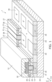
- FIG. 1 is a perspective view showing the upper portion of a semiconductor device according to the embodiment.
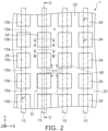
- FIG. 2 is a plan view showing the semiconductor device according to the embodiment.
- FIG. 3 is a cross-sectional view along line A-A' shown in FIG. 2 .
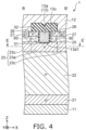
- FIG. 4 is a cross-sectional view along line B-B' shown in FIG. 2 .
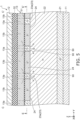
- FIG. 5 is a cross-sectional view along line C-C' shown in FIG. 2 .
- FIG. 6 is a plan view showing region D of FIG. 2 .
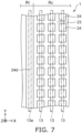
- FIG. 7 is a plan view showing a boundary vicinity between a cell part and a termination part of the semiconductor device according to the embodiment.
- FIG. 1 a portion of the configuration of the upper portion is not illustrated to show the internal configuration.
- FIG. 2 shows a surface corresponding to line E-E' shown in FIGS. 3 to 5 .
- the semiconductor device 1 includes a drain electrode 11, a source electrode 12, multiple gate electrodes 13, a semiconductor part 20, multiple gate insulating layers 31, and multiple inter-electrode insulating films 32.
- the semiconductor part 20 includes a SiC substrate 21, a drift layer 22, a current spreading layer (current diffusion layer) 23, multiple bottom layers 24, a base layer 25, multiple source layers 26, and multiple contact layers 27.
- the SiC substrate 21 functions as a drain layer.
- the portion of the semiconductor part 20 other than the SiC substrate 21 is a SiC epitaxial layer.
- the semiconductor device 1 is a trench MOSFET (Metal-Oxide-Semiconductor Field-Effect Transistor).
- an XYZ orthogonal coordinate system is employed for convenience of description.
- the arrangement direction of the drain electrode 11 and the source electrode 12 is taken as a "Z-direction"; the direction in which the gate electrodes 13 extend is taken as a "Y-direction” (a first direction); and the arrangement direction of the multiple gate electrodes 13 is taken as an "X-direction” (a second direction).
- Z-directions a direction that is from the drain electrode 11 toward the source electrode 12 also is called “up”, and the opposite direction also is called “down”, but these expressions are for convenience and are independent of the direction of gravity.
- the drain electrode 11 (a first electrode) is plate-shaped and is provided over the entire or substantially the entire lower surface of the semiconductor device 1.
- the source electrode 12 (a second electrode) also is plate-shaped, and is located in substantially the entire region of the upper surface of the semiconductor device other than where a gate pad (not illustrated) is located.
- the drain electrode 11 and the source electrode 12 are made of, for example, a metal material, e.g., aluminum (Al) and titanium (Ti).
- a cell region Rc of the semiconductor device 1 will now be described.
- the multiple gate electrodes 13 are located between the drain electrode 11 and the source electrode 12.
- the multiple gate electrodes 13 are periodically arranged along the X-direction; and each gate electrode 13 extends in the Y-direction.
- the gate electrodes 13 are formed of polysilicon that includes an impurity.
- the gate electrodes 13 are connected to a gate pad (not illustrated) at some position in the longitudinal direction (the Y-direction).
- the semiconductor part 20 is located between the drain electrode 11 and the source electrode 12.
- the gate electrode 13 is located in the upper layer portion of the semiconductor part 20.
- the semiconductor part 20 includes silicon and carbon and is made of, for example, single-crystal silicon carbide (SiC).
- the conductivity types of the portions of the semiconductor part 20 are defined by locally including impurities.
- the conductivity type of the SiC substrate 21 is the n + -type.
- the SiC substrate 21 contacts the drain electrode 11 and is connected to the drain electrode 11.
- "connected" means an electrical connection.
- the conductivity type of the drift layer 22 is the n - -type.
- the drift layer 22 is located on the SiC substrate 21 and contacts the SiC substrate 21.
- the conductivity type of the current spreading layer 23 is the n-type.
- the current spreading layer 23 is located on a portion of the drift layer 22 and contacts the drift layer 22.
- a first semiconductor layer includes the SiC substrate 21, the drift layer 22, and the current spreading layer 23.
- n + -type refers to a higher carrier concentration than the "n-type”; and the "n - -type” refers to a lower carrier concentration than the "n-type”. This is similar for the p-type as well.
- carrier concentration refers to the effective impurity concentration functioning as a donor or acceptor.
- the conductivity type of the bottom layer 24 is the p + -type.
- the bottom layer 24 contacts the drift layer 22 and is located on the drift layer 22 in a region in which the current spreading layer 23 is not located. In other words, the current spreading layer 23 and the bottom layer 24 are located on the drift layer 22.
- the multiple bottom layers 24 are arranged in a matrix configuration along the X-direction and the Y-direction.
- the bottom layers 24 are periodically arranged in both the X-direction and the Y-direction.
- Each bottom layer 24 is rectangular when viewed along the Z-direction.
- the current spreading layer 23 has a lattice shape surrounding the multiple bottom layers 24. As shown in FIG. 6 , the current spreading layer 23 includes a portion 23a located between the bottom layers 24 next to each other in the Y-direction, a portion 23b located between the bottom layers 24 next to each other in the X-direction, and a portion 23c located at a diagonal position when viewed from the bottom layer 24. The portion 23c is positioned between the portions 23a next to each other in the X-direction and between the portions 23b next to each other in the Y-direction.
- the carrier concentration of the current spreading layer 23 is greater than the carrier concentration of the drift layer 22.
- a carrier concentration C 23b of the portion 23b is not less than a carrier concentration C 23c of the portion 23c.
- the carrier concentration C 23c of the portion 23c is not less than a carrier concentration C 23a of the portion 23a.
- the carrier concentration C 23a of the portion 23a is not less than a carrier concentration C 22 of the drift layer 22.
- the carrier concentration C 23b of the portion 23b is greater than the carrier concentration C 23a of the portion 23a.
- C 23b ⁇ C 23c ⁇ C 23a ⁇ C 22 and favorably, C 23b > C 23a .
- the conductivity type of the base layer 25 (a third semiconductor layer) is the p-type.
- the carrier concentration of the p + -type bottom layer 24 is greater than the carrier concentration of the p-type base layer 25.
- the base layer 25 is located on the current spreading layer 23 and on the bottom layer 24 and contacts the current spreading layer 23 and the bottom layer 24. More specifically, the upper surface of the bottom layer 24 contacts the lower surface of the base layer 25.
- the conductivity type of the source layer 26 (a second semiconductor layer) is the n + -type.
- the conductivity type of the contact layer 27 is the p + -type.
- the source layer 26 and the contact layer 27 are located on the base layer 25 and contact the base layer 25. Accordingly, a portion of the base layer 25 is located between the current spreading layer 23 and the source layer 26.
- the source layer 26 and the contact layer 27 extend along the Y-direction.
- the source layer 26 and the contact layer 27 also may contact each other.
- the source layer 26 and the contact layer 27 contact the source electrode 12 and are connected to the source electrode 12.
- the gate insulating layer 31 is formed of silicon oxide (SiO).
- the gate electrode 13 is insulated from the semiconductor part 20 by the gate insulating layer 31 covering the side surface and the lower surface of the gate electrode 13.
- the SiC substrate 21 and the contact layer 27 are separated from the gate insulating layer 31.
- the drift layer 22 can be said to be isolated from the gate insulating layer 31 when the carrier concentration C 23a of the portion 23a is greater than the carrier concentration C 22 of the drift layer 22.
- the drift layer 22 can be said to partially contact the gate insulating layer 31 when the concentration C 22 and the concentration C 23a are equal.
- the inter-electrode insulating film 32 is formed of silicon oxide.
- the multiple inter-electrode insulating films 32 are arranged along the X-direction on the semiconductor part 20; and each inter-electrode insulating film 32 extends in the Y-direction.
- Each inter-electrode insulating film 32 is located in the region directly above the gate electrode 13 and in the two regions at the X-direction sides of the region directly above the gate electrode 13, contacts the gate electrode 13 and the source layer 26, and is separated from the contact layer 27. Thereby, the inter-electrode insulating film 32 insulates the gate electrode 13 from the source electrode 12.
- each gate electrode 13 a first portion 13a and a second portion 13b are alternately arranged along the Y-direction.
- each gate electrode 13 is formed to have a continuous body; and no interface between the first portion 13a and the second portion 13b is observed.
- the first portion 13a and the second portion 13b are periodically arranged.
- a length W1 of the first portion 13a in the Y-direction is equal to or less than a length W2 of the second portion 13b in the Y-direction. In other words, W1 ⁇ W2 .
- the lower portions of the side surfaces 13c face the base layer 25 via the gate insulating layer 31 over the full length in the Y-direction.
- the lower end of the gate electrode 13 slightly penetrates into the current spreading layer 23 and into the bottom layer 24.
- a lower surface 13d1 of the first portion 13a of the gate electrode 13 faces the portion 23a of the current spreading layer 23 via the gate insulating layer 31.
- the portion 23a of the current spreading layer 23 is located between the drift layer 22 and the first portion 13a of the gate electrode 13.
- a lower surface 13d2 of the second portion 13b of the gate electrode 13 faces the bottom layer 24 via the gate insulating layer 31.
- the bottom layer 24 is located between the drift layer 22 and the second portion 13b of the gate electrode 13.
- a termination region Rt is set at the periphery of the cell region Rc.
- a dummy gate electrode 13e is located and extends in the Y-direction.
- the dummy gate electrodes 13e are located at the two X-direction sides of the multiple gate electrodes 13 located in the cell region Rc.
- the gate insulating layer 31 is located on the side surface and on the lower surface of the dummy gate electrode 13e.
- a bottom layer 24d is located in the region directly under the dummy gate electrode 13e over the full length in the Y-direction. The bottom layer 24d continuously extends along the Y-direction. Therefore, the dummy gate electrode 13e does not face the current spreading layer 23.
- a voltage that causes the drain electrode 11 to be positive and the source electrode 12 to be negative is applied between the drain electrode 11 and the source electrode 12.
- a depletion layer is formed with the interface between an n-type semiconductor layer and a p-type semiconductor layer as a starting point; and the semiconductor device 1 is set to the off-state.
- the n-type semiconductor layer includes the drift layer 22 and the current spreading layer 23.
- the p-type semiconductor layer includes the base layer 25 and the bottom layer 24.
- an inversion layer is formed in the portion of the base layer 25 that contacts the gate insulating layer 31; and an electron current 90 flows.
- the electron current 90 flows in the current spreading layer 23 by detouring around the bottom layer 24 in the Y-direction.
- the electron current 90 flows in the order of the source electrode 12, the source layer 26, the inversion layer of the base layer 25, the current spreading layer 23, the drift layer 22, the SiC substrate 21, and the drain electrode 11. Thereby, the semiconductor device 1 is switched to the on-state.
- the potential of the base layer 25 is substantially the source potential because the base layer 25 is connected to the source electrode 12 via the contact layer 27.
- the potential of the bottom layer 24 also is substantially the source potential because the bottom layer 24 is connected to the base layer 25. Because the bottom layer 24 contacts the base layer 25, the resistance between the bottom layer 24 and the base layer 25 is low. Therefore, the potential of the bottom layer 24 is stabilized even when the semiconductor device 1 is switched at high speed. As a result, the operations of the semiconductor device 1 are stabilized.
- the holes can be quickly discharged to the source electrode 12 via the bottom layer 24, the base layer 25, and the contact layer 27 when the semiconductor device 1 is switched from the on-state to the off-state. This also stabilizes the operations of the semiconductor device 1.
- the p + -type bottom layer 24 that contacts the gate insulating layer 31 is located in the region directly under the gate electrode 13. Therefore, the application of an excessive voltage to the gate insulating layer 31 in the off-state of the semiconductor device 1 can be suppressed, and the gate insulating layer 31 can be protected. The reliability of the semiconductor device 1 is increased thereby.
- the source potential can be efficiently conducted to the bottom layer 24 because the bottom layer 24 contacts the base layer 25 that is located directly above the bottom layer 24. Thereby, even when the semiconductor device 1 is repeatedly switched on/off at high speed, the potential of the bottom layer 24 can be stabilized near the source potential. As a result, the stability of the operations of the semiconductor device 1 is increased. Problems that may occur when the potential of the bottom layer 24 cannot be stably set near the source potential are described below using a comparative example.
- the current path from the base layer 25 to the drift layer 22 can be ensured by providing the bottom layer 24 discontinuously without being in the entire region directly under the gate electrode 13 and by providing the current spreading layer 23 between the bottom layers 24.
- the operations of the MOSFET can be stably realized thereby.
- the on-resistance can be reduced by setting the carrier concentration of the current spreading layer 23 to be greater than the carrier concentration of the drift layer 22.
- the carrier concentration C 23b of the portion 23b of the current spreading layer 23 can be not less than the carrier concentration C 23c of the portion 23c and by setting the carrier concentration C 23c of the portion 23c to be not less than the carrier concentration C 23a of the portion 23a, the electron current 90 can be effectively diffused in the Y-direction, and the drift layer 22 can be effectively utilized as the current path. This also can reduce the on-resistance.
- FIG. 8 is a cross-sectional view showing a semiconductor device according to a comparative example.
- FIG. 8 is a cross section corresponding to FIG. 3 of the first embodiment.
- the bottom layer 24 is separated from the base layer 25. Also, the bottom layer 24 is continuously located in the Y-direction. In other words, the bottom layer 24 is located in the entire region directly under the gate electrode 13.
- the potential of the bottom layer 24 is unstable because the bottom layer 24 is separated from the base layer 25. Even if the bottom layer 24 is connected to the base layer 25 at some position in the longitudinal direction (the Y-direction), the internal resistance along the Y-direction of the bottom layer 24 makes it difficult for the source potential to be conducted over the entire bottom layer 24. Therefore, the potential of the bottom layer 24 undesirably fluctuates locally when the semiconductor device 101 is repeatedly switched on/off at high speed. As a result, the operations of the semiconductor device 101 become unstable.
- the dielectric breakdown electric field of the silicon oxide (SiO) forming the gate insulating layer 31 is less than the dielectric breakdown electric field of the silicon carbide (SiC) forming the semiconductor part 20; therefore, unless the bottom layer 24 is located below the gate electrode 13, there is a possibility that breakdown of the gate insulating layer 31 may be caused by an excessive voltage applied to the gate insulating layer 31 in the off-state. As a result, the reliability of the semiconductor device degrades. If, conversely, the source-drain voltage is suppressed to be low enough to avoid breakdown of the gate insulating layer 31 even when the bottom layer 24 is not included, the full characteristics of a semiconductor device using silicon carbide will not be sufficiently realized.
- the electron current that flows through the source layer 26 and the inversion layer of the base layer 25 does not easily flow into the drift layer 22; and the on-resistance is markedly increased.
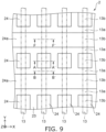
- FIG. 9 is a plan view showing a semiconductor device according to the embodiment.
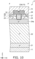
- FIG. 10 is a cross-sectional view along line F-F' shown in FIG. 9 .
- FIG. 9 The cross-sectional view along line A-A' shown in FIG. 9 is similar to FIG. 3 ; and the cross-sectional view along line B-B' is similar to FIG. 4 .
- some of the multiple bottom layers 24 extend in band shapes along the X-direction and extend over the regions directly under the second portions 13b of the multiple gate electrodes 13 arranged along the X-direction.
- a column that includes the multiple bottom layers 24 arranged in one column along the X-direction is alternately arranged in the Y-direction with one band-shaped bottom layer 24a extending in the X-direction.
- the portion 23a of the current spreading layer (current diffusion layer) 23 is depleted, and the portions 23b and 23c of the current spreading layer 23 (see FIG. 6 ) become the major path of the current.
- the peak current value flowing in the semiconductor device 2 can be suppressed thereby. As a result, the reliability of the semiconductor device 2 is increased. Otherwise, the configuration, operations, and effects of the embodiment are similar to those of the first embodiment.
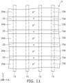
- FIG. 11 is a plan view showing a semiconductor device according to the embodiment.
- all of the bottom layers 24a have band shapes extending in the X-direction.
- the effects of the second embodiment can be more reliably obtained thereby. Otherwise, the configuration, operations, and effects of the embodiment are similar to those of the first embodiment.
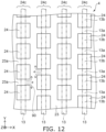
- FIG. 12 is a plan view showing a semiconductor device according to the embodiment.
- a column 24c is configured by periodically arranging the multiple bottom layers 24 in one column along the Y-direction. Multiple columns 24c are periodically arranged along the X-direction. The Y-direction positions of the bottom layers 24 are different between the columns 24c next to each other in the X-direction. In other words, the multiple bottom layers 24 when viewed along the Z-direction are arranged in a staggered configuration.
- the positions of the portions 23a of the current spreading layer (current diffusion layer) 23 can be shifted by shifting the positions of the bottom layers 24 between the columns 24c that are next to each other.
- the electron current 90 of the current spreading layer 23 can be uniformly distributed, and the on-resistance can be reduced thereby. Also, the degradation of the current spreading layer 23 and the drift layer 22 due to current concentration can be suppressed. Otherwise, the configuration, operations, and effects of the embodiment are similar to those of the first embodiment.
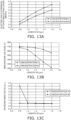
- the effects of the length W1 in the Y-direction of the first portion 13a of the gate electrode 13 (see FIG. 6 ) on the characteristics of the semiconductor device was investigated by simulation. Specifically, assuming the semiconductor device according to the first embodiment, the on-resistance, the breakdown voltage, and the electric field strength applied to the gate insulating layer 31 located on the lower surface of the gate electrode 13 were calculated for multiple conditions having different lengths W1. Two types of states having different carrier concentrations of the current spreading layer 23 were calculated for each value of the length W1.
- FIG. 13A is a graph showing the effects of the length W1 on the electric field strength, in which the horizontal axis is the length W1, and the vertical axis is the electric field strength applied to the gate insulating layer;
- FIG. 13B is a graph showing the effects of the length W1 on the breakdown voltage, in which the horizontal axis is the length W1, and the vertical axis is the breakdown voltage;
- FIG. 13C is a graph showing the effects of the length W1 on the on-resistance, in which the horizontal axis is the length W1, and the vertical axis is the relative value of the on-resistance.
- the "concentration A" is less than the "concentration B" in FIGS. 13A to 13C .
- the electric field strength that was applied to the gate insulating layer 31 located on the lower surface of the gate electrode 13 increased as the length W1 increased. Therefore, as shown in FIG. 13B , the breakdown voltage of the semiconductor device decreased as the length W1 increased. As shown in FIG. 13C , the on-resistance substantially does not change when the length W1 was not less than 1 ⁇ m.
- a semiconductor device can be realized in which breakdown can be suppressed and stability of the operations can be improved.
- first and second portions 13a and 13b of the gate electrode 13 are periodically arranged along the longitudinal direction of the gate electrode 13 (the Y-direction)
- the arrangement is not limited thereto.
- the arrangement of the first and second portions 13a and 13b may not be periodic.
- the first portion 13a and the second portion 13b may be arranged along the width direction of the gate electrode 13 (the X-direction).
- Embodiments include the following aspects.
- a semiconductor device comprising:
- a length in the first direction of the first portion is not more than a length in the first direction of the second portion.
- a carrier concentration of a portion of the first semiconductor layer located between the fourth semiconductor layers next to each other in the second direction is greater than a carrier concentration of a portion of the first semiconductor layer located between the fourth semiconductor layers next to each other in the first direction.
Landscapes
- Electrodes Of Semiconductors (AREA)
Abstract
A semiconductor device includes a first electrode, a second electrode, a third electrode located between the first electrode and the second electrode, a first semiconductor layer connected to the first electrode, a second semiconductor layer connected to the second electrode, a third semiconductor layer of a second conductivity type, and a fourth semiconductor layer of the second conductivity type. The third electrode includes first and second portions. The first semiconductor layer faces the first portion via an insulating layer. The first and second semiconductor layers are of a first conductivity type and include silicon and carbon. A carrier concentration of the fourth semiconductor layer is greater than a carrier concentration of the third semiconductor layer.
Description
- Embodiments relate to a semiconductor device.
- Semiconductor devices that use silicon carbide as a semiconductor material are being developed to improve the balance between the on-resistance and the breakdown voltage of the semiconductor device. It is desirable to suppress breakdown due to the application of high voltages and to improve the operation stability of such a semiconductor device.
-
-
FIG. 1 is a perspective view showing an upper portion of a semiconductor device according to a first embodiment; -
FIG. 2 is a plan view showing the semiconductor device according to the first embodiment; -
FIG. 3 is a cross-sectional view along line A-A' shown inFIG. 2 ; -
FIG. 4 is a cross-sectional view along line B-B' shown inFIG. 2 ; -
FIG. 5 is a cross-sectional view along line C-C' shown inFIG. 2 ; -
FIG. 6 is a plan view showing region D ofFIG. 2 ; -
FIG. 7 is a plan view showing a boundary vicinity between a cell part and a termination part of the semiconductor device according to the first embodiment; -
FIG. 8 is a cross-sectional view showing a semiconductor device according to a comparative example; -
FIG. 9 is a plan view showing a semiconductor device according to a second embodiment; -
FIG. 10 is a cross-sectional view along line F-F' shown inFIG. 9 ; -
FIG. 11 is a plan view showing a semiconductor device according to a third embodiment; -
FIG. 12 is a plan view showing a semiconductor device according to a fourth embodiment; and -
FIG. 13A is a graph showing the effects of the length W1 on the electric field strength, in which the horizontal axis is the length W1, and the vertical axis is the electric field strength applied to the gate insulating layer;FIG. 13B is a graph showing the effects of the length W1 on the breakdown voltage, in which the horizontal axis is the length W1, and the vertical axis is the breakdown voltage; andFIG. 13C is a graph showing the effects of the length W1 on the on-resistance, in which the horizontal axis is the length W1, and the vertical axis is the relative value of the on-resistance. - In general, according to one embodiment, a semiconductor device includes a first electrode, a second electrode, a third electrode located between the first electrode and the second electrode, a first semiconductor layer connected to the first electrode, a second semiconductor layer connected to the second electrode, a third semiconductor layer of a second conductivity type, and a fourth semiconductor layer of the second conductivity type. The third electrode extends in a first direction and includes a first portion and a second portion. The first semiconductor layer faces the first portion via an insulating layer. The first semiconductor layer is of a first conductivity type and includes silicon and carbon. The second semiconductor layer is of the first conductivity type and includes silicon and carbon. At least a portion of the third semiconductor layer is located between the first semiconductor layer and the second semiconductor layer. The third semiconductor layer contacts the first and second semiconductor layers, faces the third electrode via the insulating layer, and includes silicon and carbon. At least a portion of the fourth semiconductor layer is located between the first semiconductor layer and the second portion. The fourth semiconductor layer faces the second portion via the insulating layer. The fourth semiconductor layer contacts the third semiconductor layer and includes silicon and carbon. A carrier concentration of the fourth semiconductor layer is greater than a carrier concentration of the third semiconductor layer.
-
FIG. 1 is a perspective view showing the upper portion of a semiconductor device according to the embodiment. -
FIG. 2 is a plan view showing the semiconductor device according to the embodiment. -
FIG. 3 is a cross-sectional view along line A-A' shown inFIG. 2 . -
FIG. 4 is a cross-sectional view along line B-B' shown inFIG. 2 . -
FIG. 5 is a cross-sectional view along line C-C' shown inFIG. 2 . -
FIG. 6 is a plan view showing region D ofFIG. 2 . -
FIG. 7 is a plan view showing a boundary vicinity between a cell part and a termination part of the semiconductor device according to the embodiment. - In
FIG. 1 , a portion of the configuration of the upper portion is not illustrated to show the internal configuration. -
FIG. 2 shows a surface corresponding to line E-E' shown inFIGS. 3 to 5 . - The drawings are schematic or conceptual, and are enhanced and simplified as appropriate. The shapes and dimensional ratios of the components do not always match between the drawings. This is similar for the other drawings described below as well.
- As shown in
FIGS. 1 to 6 , thesemiconductor device 1 according to the embodiment includes adrain electrode 11, asource electrode 12,multiple gate electrodes 13, asemiconductor part 20, multiple gateinsulating layers 31, and multiple inter-electrodeinsulating films 32. Thesemiconductor part 20 includes aSiC substrate 21, adrift layer 22, a current spreading layer (current diffusion layer) 23,multiple bottom layers 24, abase layer 25,multiple source layers 26, andmultiple contact layers 27. TheSiC substrate 21 functions as a drain layer. The portion of thesemiconductor part 20 other than theSiC substrate 21 is a SiC epitaxial layer. Thesemiconductor device 1 is a trench MOSFET (Metal-Oxide-Semiconductor Field-Effect Transistor). - In the specification hereinbelow, an XYZ orthogonal coordinate system is employed for convenience of description. The arrangement direction of the
drain electrode 11 and thesource electrode 12 is taken as a "Z-direction"; the direction in which thegate electrodes 13 extend is taken as a "Y-direction" (a first direction); and the arrangement direction of themultiple gate electrodes 13 is taken as an "X-direction" (a second direction). Among the Z-directions, a direction that is from thedrain electrode 11 toward thesource electrode 12 also is called "up", and the opposite direction also is called "down", but these expressions are for convenience and are independent of the direction of gravity. - The drain electrode 11 (a first electrode) is plate-shaped and is provided over the entire or substantially the entire lower surface of the
semiconductor device 1. The source electrode 12 (a second electrode) also is plate-shaped, and is located in substantially the entire region of the upper surface of the semiconductor device other than where a gate pad (not illustrated) is located. Thedrain electrode 11 and thesource electrode 12 are made of, for example, a metal material, e.g., aluminum (Al) and titanium (Ti). - A cell region Rc of the
semiconductor device 1 will now be described. - The multiple gate electrodes 13 (third electrodes) are located between the
drain electrode 11 and thesource electrode 12. Themultiple gate electrodes 13 are periodically arranged along the X-direction; and eachgate electrode 13 extends in the Y-direction. For example, thegate electrodes 13 are formed of polysilicon that includes an impurity. Thegate electrodes 13 are connected to a gate pad (not illustrated) at some position in the longitudinal direction (the Y-direction). - The
semiconductor part 20 is located between thedrain electrode 11 and thesource electrode 12. Thegate electrode 13 is located in the upper layer portion of thesemiconductor part 20. Thesemiconductor part 20 includes silicon and carbon and is made of, for example, single-crystal silicon carbide (SiC). The conductivity types of the portions of thesemiconductor part 20 are defined by locally including impurities. - The conductivity type of the
SiC substrate 21 is the n+-type. TheSiC substrate 21 contacts thedrain electrode 11 and is connected to thedrain electrode 11. In the specification, "connected" means an electrical connection. The conductivity type of thedrift layer 22 is the n--type. Thedrift layer 22 is located on theSiC substrate 21 and contacts theSiC substrate 21. The conductivity type of the current spreadinglayer 23 is the n-type. The current spreadinglayer 23 is located on a portion of thedrift layer 22 and contacts thedrift layer 22. A first semiconductor layer includes theSiC substrate 21, thedrift layer 22, and the current spreadinglayer 23. - The "n+-type" refers to a higher carrier concentration than the "n-type"; and the "n--type" refers to a lower carrier concentration than the "n-type". This is similar for the p-type as well. The "carrier concentration" refers to the effective impurity concentration functioning as a donor or acceptor.
- The conductivity type of the bottom layer 24 (a fourth semiconductor layer) is the p+-type. The
bottom layer 24 contacts thedrift layer 22 and is located on thedrift layer 22 in a region in which the current spreadinglayer 23 is not located. In other words, the current spreadinglayer 23 and thebottom layer 24 are located on thedrift layer 22. According to the embodiment as shown inFIG. 2 , the multiplebottom layers 24 are arranged in a matrix configuration along the X-direction and the Y-direction. The bottom layers 24 are periodically arranged in both the X-direction and the Y-direction. Eachbottom layer 24 is rectangular when viewed along the Z-direction. - The current spreading
layer 23 has a lattice shape surrounding the multiple bottom layers 24. As shown inFIG. 6 , the current spreadinglayer 23 includes aportion 23a located between thebottom layers 24 next to each other in the Y-direction, aportion 23b located between thebottom layers 24 next to each other in the X-direction, and aportion 23c located at a diagonal position when viewed from thebottom layer 24. Theportion 23c is positioned between theportions 23a next to each other in the X-direction and between theportions 23b next to each other in the Y-direction. - The carrier concentration of the current spreading
layer 23 is greater than the carrier concentration of thedrift layer 22. In the current spreadinglayer 23, a carrier concentration C23b of theportion 23b is not less than a carrier concentration C23c of theportion 23c. The carrier concentration C23c of theportion 23c is not less than a carrier concentration C23a of theportion 23a. The carrier concentration C23a of theportion 23a is not less than a carrier concentration C22 of thedrift layer 22. Favorably, the carrier concentration C23b of theportion 23b is greater than the carrier concentration C23a of theportion 23a. In other words, C23b ≥ C23c ≥ C23a ≥ C 22 , and favorably, C23b > C23a. - The conductivity type of the base layer 25 (a third semiconductor layer) is the p-type. The carrier concentration of the p+-
type bottom layer 24 is greater than the carrier concentration of the p-type base layer 25. Thebase layer 25 is located on the current spreadinglayer 23 and on thebottom layer 24 and contacts the current spreadinglayer 23 and thebottom layer 24. More specifically, the upper surface of thebottom layer 24 contacts the lower surface of thebase layer 25. - The conductivity type of the source layer 26 (a second semiconductor layer) is the n+-type. The conductivity type of the
contact layer 27 is the p+-type. Thesource layer 26 and thecontact layer 27 are located on thebase layer 25 and contact thebase layer 25. Accordingly, a portion of thebase layer 25 is located between the current spreadinglayer 23 and thesource layer 26. Thesource layer 26 and thecontact layer 27 extend along the Y-direction. Thesource layer 26 and thecontact layer 27 also may contact each other. Thesource layer 26 and thecontact layer 27 contact thesource electrode 12 and are connected to thesource electrode 12. - For example, the
gate insulating layer 31 is formed of silicon oxide (SiO). Thegate electrode 13 is insulated from thesemiconductor part 20 by thegate insulating layer 31 covering the side surface and the lower surface of thegate electrode 13. In thesemiconductor part 20, the upper surface of the current spreadinglayer 23, the upper surface of thebottom layer 24, the side surface of thebase layer 25, and the side surface of thesource layer 26 contact thegate insulating layer 31. On the other hand, theSiC substrate 21 and thecontact layer 27 are separated from thegate insulating layer 31. Thedrift layer 22 can be said to be isolated from thegate insulating layer 31 when the carrier concentration C23a of theportion 23a is greater than the carrier concentration C22 of thedrift layer 22. On the other hand, thedrift layer 22 can be said to partially contact thegate insulating layer 31 when the concentration C22 and the concentration C23a are equal. - For example, the inter-electrode insulating
film 32 is formed of silicon oxide. The multiple inter-electrodeinsulating films 32 are arranged along the X-direction on thesemiconductor part 20; and each inter-electrode insulatingfilm 32 extends in the Y-direction. Each inter-electrode insulatingfilm 32 is located in the region directly above thegate electrode 13 and in the two regions at the X-direction sides of the region directly above thegate electrode 13, contacts thegate electrode 13 and thesource layer 26, and is separated from thecontact layer 27. Thereby, the inter-electrode insulatingfilm 32 insulates thegate electrode 13 from thesource electrode 12. - In each
gate electrode 13, afirst portion 13a and asecond portion 13b are alternately arranged along the Y-direction. For example, eachgate electrode 13 is formed to have a continuous body; and no interface between thefirst portion 13a and thesecond portion 13b is observed. For example, thefirst portion 13a and thesecond portion 13b are periodically arranged. In an example, a length W1 of thefirst portion 13a in the Y-direction is equal to or less than a length W2 of thesecond portion 13b in the Y-direction. In other words, W1 ≤ W2. - The upper portions of side surfaces 13c of the
gate electrode 13 at the two X-direction sides of thegate electrode 13 face thesource layer 26 via thegate insulating layer 31 over the full length in the Y-direction. The lower portions of the side surfaces 13c face thebase layer 25 via thegate insulating layer 31 over the full length in the Y-direction. - The lower end of the
gate electrode 13 slightly penetrates into the current spreadinglayer 23 and into thebottom layer 24. As shown inFIG. 4 , a lower surface 13d1 of thefirst portion 13a of thegate electrode 13 faces theportion 23a of the current spreadinglayer 23 via thegate insulating layer 31. In other words, theportion 23a of the current spreadinglayer 23 is located between thedrift layer 22 and thefirst portion 13a of thegate electrode 13. On the other hand, as shown inFIG. 3 , a lower surface 13d2 of thesecond portion 13b of thegate electrode 13 faces thebottom layer 24 via thegate insulating layer 31. In other words, thebottom layer 24 is located between thedrift layer 22 and thesecond portion 13b of thegate electrode 13. Thus, in thegate electrode 13, thefirst portion 13a that faces the n-type current spreadinglayer 23 and thesecond portion 13b that faces the p+-type bottom layer 24 are alternately arranged in the Y-direction. - In the
semiconductor device 1 as shown inFIG. 7 , a termination region Rt is set at the periphery of the cell region Rc. At the boundary part of the cell region Rc and the termination region Rt, adummy gate electrode 13e is located and extends in the Y-direction. Thedummy gate electrodes 13e are located at the two X-direction sides of themultiple gate electrodes 13 located in the cell region Rc. Thegate insulating layer 31 is located on the side surface and on the lower surface of thedummy gate electrode 13e. Abottom layer 24d is located in the region directly under thedummy gate electrode 13e over the full length in the Y-direction. Thebottom layer 24d continuously extends along the Y-direction. Therefore, thedummy gate electrode 13e does not face the current spreadinglayer 23. - Operations of the
semiconductor device 1 according to the embodiment will now be described. - A voltage that causes the
drain electrode 11 to be positive and thesource electrode 12 to be negative is applied between thedrain electrode 11 and thesource electrode 12. Thereby, a depletion layer is formed with the interface between an n-type semiconductor layer and a p-type semiconductor layer as a starting point; and thesemiconductor device 1 is set to the off-state. The n-type semiconductor layer includes thedrift layer 22 and the current spreadinglayer 23. The p-type semiconductor layer includes thebase layer 25 and thebottom layer 24. By providing the p+-type bottom layer 24 that contacts thegate insulating layer 31 in the region directly under thegate electrode 13, the voltage that is applied to thegate insulating layer 31 can be suppressed at this time. - When a potential that is not less than a threshold is applied to the
gate electrode 13 in this state, an inversion layer is formed in the portion of thebase layer 25 that contacts thegate insulating layer 31; and an electron current 90 flows. As shown inFIG. 5 , the electron current 90 flows in the current spreadinglayer 23 by detouring around thebottom layer 24 in the Y-direction. In other words, the electron current 90 flows in the order of thesource electrode 12, thesource layer 26, the inversion layer of thebase layer 25, the current spreadinglayer 23, thedrift layer 22, theSiC substrate 21, and thedrain electrode 11. Thereby, thesemiconductor device 1 is switched to the on-state. - The potential of the
base layer 25 is substantially the source potential because thebase layer 25 is connected to thesource electrode 12 via thecontact layer 27. The potential of thebottom layer 24 also is substantially the source potential because thebottom layer 24 is connected to thebase layer 25. Because thebottom layer 24 contacts thebase layer 25, the resistance between thebottom layer 24 and thebase layer 25 is low. Therefore, the potential of thebottom layer 24 is stabilized even when thesemiconductor device 1 is switched at high speed. As a result, the operations of thesemiconductor device 1 are stabilized. - Because the
bottom layer 24 is connected to thebase layer 25 with low resistance, the holes can be quickly discharged to thesource electrode 12 via thebottom layer 24, thebase layer 25, and thecontact layer 27 when thesemiconductor device 1 is switched from the on-state to the off-state. This also stabilizes the operations of thesemiconductor device 1. - Effects of the embodiment will now be described.
- In the
semiconductor device 1 according to the embodiment, the p+-type bottom layer 24 that contacts thegate insulating layer 31 is located in the region directly under thegate electrode 13. Therefore, the application of an excessive voltage to thegate insulating layer 31 in the off-state of thesemiconductor device 1 can be suppressed, and thegate insulating layer 31 can be protected. The reliability of thesemiconductor device 1 is increased thereby. - Also, the source potential can be efficiently conducted to the
bottom layer 24 because thebottom layer 24 contacts thebase layer 25 that is located directly above thebottom layer 24. Thereby, even when thesemiconductor device 1 is repeatedly switched on/off at high speed, the potential of thebottom layer 24 can be stabilized near the source potential. As a result, the stability of the operations of thesemiconductor device 1 is increased. Problems that may occur when the potential of thebottom layer 24 cannot be stably set near the source potential are described below using a comparative example. - The current path from the
base layer 25 to thedrift layer 22 can be ensured by providing thebottom layer 24 discontinuously without being in the entire region directly under thegate electrode 13 and by providing the current spreadinglayer 23 between the bottom layers 24. The operations of the MOSFET can be stably realized thereby. - The on-resistance can be reduced by setting the carrier concentration of the current spreading
layer 23 to be greater than the carrier concentration of thedrift layer 22. In particular, by setting the carrier concentration C23b of theportion 23b of the current spreadinglayer 23 to be not less than the carrier concentration C23c of theportion 23c and by setting the carrier concentration C23c of theportion 23c to be not less than the carrier concentration C23a of theportion 23a, the electron current 90 can be effectively diffused in the Y-direction, and thedrift layer 22 can be effectively utilized as the current path. This also can reduce the on-resistance. -
FIG. 8 is a cross-sectional view showing a semiconductor device according to a comparative example. -
FIG. 8 is a cross section corresponding toFIG. 3 of the first embodiment. - In the
semiconductor device 101 according to the comparative example as shown inFIG. 8 , thebottom layer 24 is separated from thebase layer 25. Also, thebottom layer 24 is continuously located in the Y-direction. In other words, thebottom layer 24 is located in the entire region directly under thegate electrode 13. - In the comparative example, the potential of the
bottom layer 24 is unstable because thebottom layer 24 is separated from thebase layer 25. Even if thebottom layer 24 is connected to thebase layer 25 at some position in the longitudinal direction (the Y-direction), the internal resistance along the Y-direction of thebottom layer 24 makes it difficult for the source potential to be conducted over the entirebottom layer 24. Therefore, the potential of thebottom layer 24 undesirably fluctuates locally when thesemiconductor device 101 is repeatedly switched on/off at high speed. As a result, the operations of thesemiconductor device 101 become unstable. - The dielectric breakdown electric field of the silicon oxide (SiO) forming the
gate insulating layer 31 is less than the dielectric breakdown electric field of the silicon carbide (SiC) forming thesemiconductor part 20; therefore, unless thebottom layer 24 is located below thegate electrode 13, there is a possibility that breakdown of thegate insulating layer 31 may be caused by an excessive voltage applied to thegate insulating layer 31 in the off-state. As a result, the reliability of the semiconductor device degrades. If, conversely, the source-drain voltage is suppressed to be low enough to avoid breakdown of thegate insulating layer 31 even when thebottom layer 24 is not included, the full characteristics of a semiconductor device using silicon carbide will not be sufficiently realized. Or, if thebottom layer 24 is elongated upward from the state shown inFIG. 8 to contact thebase layer 25, the electron current that flows through thesource layer 26 and the inversion layer of thebase layer 25 does not easily flow into thedrift layer 22; and the on-resistance is markedly increased. -
FIG. 9 is a plan view showing a semiconductor device according to the embodiment. -
FIG. 10 is a cross-sectional view along line F-F' shown inFIG. 9 . - The cross-sectional view along line A-A' shown in
FIG. 9 is similar toFIG. 3 ; and the cross-sectional view along line B-B' is similar toFIG. 4 . - In the
semiconductor device 2 according to the embodiment as shown inFIGS. 9 and10 , some of the multiplebottom layers 24 extend in band shapes along the X-direction and extend over the regions directly under thesecond portions 13b of themultiple gate electrodes 13 arranged along the X-direction. In the example shown inFIG. 9 , a column that includes the multiplebottom layers 24 arranged in one column along the X-direction is alternately arranged in the Y-direction with one band-shapedbottom layer 24a extending in the X-direction. - According to the embodiment, when a higher voltage than normal is applied between the
drain electrode 11 and thesource electrode 12 due to, for example, a short-circuit of a load connected to thesemiconductor device 2, etc., theportion 23a of the current spreading layer (current diffusion layer) 23 is depleted, and theportions FIG. 6 ) become the major path of the current. The peak current value flowing in thesemiconductor device 2 can be suppressed thereby. As a result, the reliability of thesemiconductor device 2 is increased. Otherwise, the configuration, operations, and effects of the embodiment are similar to those of the first embodiment. -
FIG. 11 is a plan view showing a semiconductor device according to the embodiment. - In the
semiconductor device 3 according to the embodiment as shown inFIG. 11 , all of thebottom layers 24a have band shapes extending in the X-direction. The effects of the second embodiment can be more reliably obtained thereby. Otherwise, the configuration, operations, and effects of the embodiment are similar to those of the first embodiment. -
FIG. 12 is a plan view showing a semiconductor device according to the embodiment. - In the
semiconductor device 4 according to the embodiment as shown inFIG. 12 , acolumn 24c is configured by periodically arranging the multiplebottom layers 24 in one column along the Y-direction.Multiple columns 24c are periodically arranged along the X-direction. The Y-direction positions of the bottom layers 24 are different between thecolumns 24c next to each other in the X-direction. In other words, the multiplebottom layers 24 when viewed along the Z-direction are arranged in a staggered configuration. - According to the embodiment, the positions of the
portions 23a of the current spreading layer (current diffusion layer) 23 can be shifted by shifting the positions of the bottom layers 24 between thecolumns 24c that are next to each other. Theelectron current 90 of the current spreadinglayer 23 can be uniformly distributed, and the on-resistance can be reduced thereby. Also, the degradation of the current spreadinglayer 23 and thedrift layer 22 due to current concentration can be suppressed. Otherwise, the configuration, operations, and effects of the embodiment are similar to those of the first embodiment. - For test examples, the effects of the length W1 in the Y-direction of the
first portion 13a of the gate electrode 13 (seeFIG. 6 ) on the characteristics of the semiconductor device was investigated by simulation. Specifically, assuming the semiconductor device according to the first embodiment, the on-resistance, the breakdown voltage, and the electric field strength applied to thegate insulating layer 31 located on the lower surface of thegate electrode 13 were calculated for multiple conditions having different lengths W1. Two types of states having different carrier concentrations of the current spreadinglayer 23 were calculated for each value of the length W1. -
FIG. 13A is a graph showing the effects of the length W1 on the electric field strength, in which the horizontal axis is the length W1, and the vertical axis is the electric field strength applied to the gate insulating layer;FIG. 13B is a graph showing the effects of the length W1 on the breakdown voltage, in which the horizontal axis is the length W1, and the vertical axis is the breakdown voltage; andFIG. 13C is a graph showing the effects of the length W1 on the on-resistance, in which the horizontal axis is the length W1, and the vertical axis is the relative value of the on-resistance. The "concentration A" is less than the "concentration B" inFIGS. 13A to 13C . - As shown in
FIG. 13A , the electric field strength that was applied to thegate insulating layer 31 located on the lower surface of thegate electrode 13 increased as the length W1 increased. Therefore, as shown inFIG. 13B , the breakdown voltage of the semiconductor device decreased as the length W1 increased. As shown inFIG. 13C , the on-resistance substantially does not change when the length W1 was not less than 1 µm. - According to the embodiments described above, a semiconductor device can be realized in which breakdown can be suppressed and stability of the operations can be improved.
- Although an example is shown in the embodiments described above in which the first and
second portions gate electrode 13 are periodically arranged along the longitudinal direction of the gate electrode 13 (the Y-direction), the arrangement is not limited thereto. For example, the arrangement of the first andsecond portions first portion 13a and thesecond portion 13b may be arranged along the width direction of the gate electrode 13 (the X-direction). - While certain embodiments have been described, these embodiments have been presented by way of example only, and are not intended to limit the scope of the inventions. Indeed, the novel embodiments described herein may be embodied in a variety of other forms; furthermore, various omissions, substitutions and changes in the form of the embodiments described herein may be made without departing from the spirit of the inventions. The accompanying claims and their equivalents are intended to cover such forms or modifications as would fall within the scope and spirit of the inventions.
- Embodiments include the following aspects.
- A semiconductor device, comprising:
- a first electrode;
- a second electrode;
- a third electrode located between the first electrode and the second electrode, the third electrode extending in a first direction and including a first portion and a second portion;
- a first semiconductor layer connected to the first electrode, the first semiconductor layer facing the first portion via an insulating layer, the first semiconductor layer being of a first conductivity type and including silicon and carbon;
- a second semiconductor layer connected to the second electrode, the second semiconductor layer being of the first conductivity type and including silicon and carbon;
- a third semiconductor layer of a second conductivity type, at least a portion of the third semiconductor layer being located between the first semiconductor layer and the second semiconductor layer, the third semiconductor layer contacting the first and second semiconductor layers, facing the third electrode via the insulating layer, and including silicon and carbon; and
- a fourth semiconductor layer of the second conductivity type, at least a portion of the fourth semiconductor layer being located between the first semiconductor layer and the second portion, the fourth semiconductor layer facing the second portion via the insulating layer, the fourth semiconductor layer contacting the third semiconductor layer and including silicon and carbon, a carrier concentration of the fourth semiconductor layer being greater than a carrier concentration of the third semiconductor layer.
- The device according to
note 1, wherein
a surface of the fourth semiconductor layer at the second electrode side contacts the third semiconductor layer and the insulating layer. - The device according to
note
a surface of the first semiconductor layer faces the first portion contacts the insulating layer. - The device according to any one of
notes 1 to 3, wherein
a length in the first direction of the first portion is not more than a length in the first direction of the second portion. - The device according to any one of
notes 1 to 4, wherein
the first portion and the second portion of the third electrode are alternately arranged along the first direction. - The device according to note 5, wherein
the first portion and the second portion are periodically arranged. - The device according to any one of
notes 1 to 6, wherein
the second semiconductor layer extends in the first direction and faces the third electrode via the insulating layer. - The device according to any one of
notes 1 to 7, wherein - a plurality of the third electrodes is arranged along a second direction crossing the first direction, and
- a plurality of the fourth semiconductor layers is arranged along the first direction.
- The device according to
note 8, wherein
the fourth semiconductor layers are arranged in a matrix configuration along the first and second directions. - The device according to
note 8, wherein
a portion of the plurality of fourth semiconductor layers extends across regions directly under the second portions of a plurality of the third electrodes arranged along the second direction. - The device according to
note 8, wherein
the plurality of fourth semiconductor layers extends in the second direction and is located in regions directly under the plurality of third electrodes. - The device according to
note 8, wherein - columns each include a plurality of the fourth semiconductor layers arranged in one column along the first direction, and
- positions in the first direction of the fourth semiconductor layers included in the columns are different between the columns next to each other in the second direction.
- The device according to
note 9 or 12, wherein
a carrier concentration of a portion of the first semiconductor layer located between the fourth semiconductor layers next to each other in the second direction is greater than a carrier concentration of a portion of the first semiconductor layer located between the fourth semiconductor layers next to each other in the first direction. - It is explicitly stated that all features disclosed in the description and/or the claims are intended to be disclosed separately and independently from each other for the purpose of original disclosure as well as for the purpose of restricting the claimed invention independent of the composition of the features in the embodiments and/or the claims. It is explicitly stated that all value ranges or indications of groups of entities disclose every possible intermediate value or intermediate entity for the purpose of original disclosure as well as for the purpose of restricting the claimed invention, in particular as limits of value ranges.
Claims (13)
- A semiconductor device, comprising:a first electrode (11);a second electrode (12);a third electrode (13) located between the first electrode and the second electrode, the third electrode extending in a first direction (Y) and including a first portion (13a) and a second portion (13b);a first semiconductor layer (21+22+23) connected to the first electrode, the first semiconductor layer facing the first portion via an insulating layer (31), the first semiconductor layer being of a first conductivity type (n) and including silicon and carbon;a second semiconductor layer (26) connected to the second electrode, the second semiconductor layer being of the first conductivity type and including silicon and carbon;a third semiconductor layer (25) of a second conductivity type (p), at least a portion of the third semiconductor layer being located between the first semiconductor layer and the second semiconductor layer, the third semiconductor layer contacting the first and second semiconductor layers, facing the third electrode via the insulating layer, and including silicon and carbon; anda fourth semiconductor layer (24) of the second conductivity type, at least a portion of the fourth semiconductor layer being located between the first semiconductor layer and the second portion, the fourth semiconductor layer facing the second portion via the insulating layer, the fourth semiconductor layer contacting the third semiconductor layer and including silicon and carbon, a carrier concentration of the fourth semiconductor layer being greater than a carrier concentration of the third semiconductor layer.
- The device according to claim 1, wherein
a surface of the fourth semiconductor layer at the second electrode side contacts the third semiconductor layer and the insulating layer. - The device according to claim 1 or 2, wherein
a surface of the first semiconductor layer faces the first portion contacts the insulating layer. - The device according to any one of claims 1 to 3, wherein
a length (W1) in the first direction of the first portion is not more than a length (W2) in the first direction of the second portion. - The device according to any one of claims 1 to 4, wherein
the first portion and the second portion of the third electrode are alternately arranged along the first direction. - The device according to claim 5, wherein
the first portion and the second portion are periodically arranged. - The device according to any one of claims 1 to 6, wherein
the second semiconductor layer extends in the first direction and faces the third electrode via the insulating layer. - The device according to any one of claims 1 to 7, whereina plurality of the third electrodes is arranged along a second direction (X) crossing the first direction, anda plurality of the fourth semiconductor layers is arranged along the first direction.
- The device according to claim 8, wherein
the fourth semiconductor layers are arranged in a matrix configuration along the first and second directions. - The device according to claim 8, wherein
a portion of the plurality of fourth semiconductor layers extends across regions directly under the second portions of a plurality of the third electrodes arranged along the second direction. - The device according to claim 8, wherein
the plurality of fourth semiconductor layers extends in the second direction and is located in regions directly under the plurality of third electrodes. - The device according to claim 8, whereincolumns (24c) each include a plurality of the fourth semiconductor layers arranged in one column along the first direction, andpositions in the first direction of the fourth semiconductor layers included in the columns are different between the columns next to each other in the second direction.
- The device according to claim 9 or 12, wherein
a carrier concentration of a portion (23b) of the first semiconductor layer located between the fourth semiconductor layers next to each other in the second direction is greater than a carrier concentration of a portion (23a) of the first semiconductor layer located between the fourth semiconductor layers next to each other in the first direction.
Applications Claiming Priority (1)
| Application Number | Priority Date | Filing Date | Title |
|---|---|---|---|
| JP2022147107A JP2024042414A (en) | 2022-09-15 | 2022-09-15 | semiconductor equipment |
Publications (1)
| Publication Number | Publication Date |
|---|---|
| EP4340040A1 true EP4340040A1 (en) | 2024-03-20 |
Family
ID=85076374
Family Applications (1)
| Application Number | Title | Priority Date | Filing Date |
|---|---|---|---|
| EP23153228.4A Pending EP4340040A1 (en) | 2022-09-15 | 2023-01-25 | Semiconductor device |
Country Status (4)
| Country | Link |
|---|---|
| US (1) | US20240096966A1 (en) |
| EP (1) | EP4340040A1 (en) |
| JP (1) | JP2024042414A (en) |
| CN (1) | CN117712138A (en) |
Citations (4)
| Publication number | Priority date | Publication date | Assignee | Title |
|---|---|---|---|---|
| US20040195618A1 (en) * | 2003-04-07 | 2004-10-07 | Wataru Saito | Insulated gate semiconductor device |
| US7227225B2 (en) * | 2003-04-23 | 2007-06-05 | Kabushiki Kaisha Toshiba | Semiconductor device having a vertical MOS trench gate structure |
| US8193564B2 (en) * | 2008-02-13 | 2012-06-05 | Denso Corporation | Silicon carbide semiconductor device including deep layer |
| US20220052170A1 (en) * | 2020-08-11 | 2022-02-17 | Maxpower Semiconductor, Inc. | Mosfet with distributed doped p-shield zones under trenches |
Family Cites Families (5)
| Publication number | Priority date | Publication date | Assignee | Title |
|---|---|---|---|---|
| JP2010147222A (en) * | 2008-12-18 | 2010-07-01 | Denso Corp | Silicon carbide semiconductor device and method of manufacturing the same |
| JP5531787B2 (en) * | 2010-05-31 | 2014-06-25 | 株式会社デンソー | Silicon carbide semiconductor device and manufacturing method thereof |
| US9887287B1 (en) * | 2016-12-08 | 2018-02-06 | Cree, Inc. | Power semiconductor devices having gate trenches with implanted sidewalls and related methods |
| JP2019087611A (en) * | 2017-11-06 | 2019-06-06 | トヨタ自動車株式会社 | Switching element and manufacturing method thereof |
| JP7180402B2 (en) * | 2019-01-21 | 2022-11-30 | 株式会社デンソー | semiconductor equipment |
-
2022
- 2022-09-15 JP JP2022147107A patent/JP2024042414A/en active Pending
- 2022-12-13 CN CN202211602911.2A patent/CN117712138A/en active Pending
-
2023
- 2023-01-25 EP EP23153228.4A patent/EP4340040A1/en active Pending
- 2023-01-26 US US18/160,002 patent/US20240096966A1/en active Pending
Patent Citations (4)
| Publication number | Priority date | Publication date | Assignee | Title |
|---|---|---|---|---|
| US20040195618A1 (en) * | 2003-04-07 | 2004-10-07 | Wataru Saito | Insulated gate semiconductor device |
| US7227225B2 (en) * | 2003-04-23 | 2007-06-05 | Kabushiki Kaisha Toshiba | Semiconductor device having a vertical MOS trench gate structure |
| US8193564B2 (en) * | 2008-02-13 | 2012-06-05 | Denso Corporation | Silicon carbide semiconductor device including deep layer |
| US20220052170A1 (en) * | 2020-08-11 | 2022-02-17 | Maxpower Semiconductor, Inc. | Mosfet with distributed doped p-shield zones under trenches |
Also Published As
| Publication number | Publication date |
|---|---|
| CN117712138A (en) | 2024-03-15 |
| US20240096966A1 (en) | 2024-03-21 |
| JP2024042414A (en) | 2024-03-28 |
Similar Documents
| Publication | Publication Date | Title |
|---|---|---|
| JP5198030B2 (en) | Semiconductor element | |
| EP3047523B1 (en) | High voltage mosfet devices and methods of making the devices | |
| JP4623956B2 (en) | IGBT | |
| US8283720B2 (en) | Power semiconductor device | |
| US8735982B2 (en) | Semiconductor device with superjunction structure | |
| US20230387194A1 (en) | Field effect transistor and method of manufacturing the same | |
| US10872975B2 (en) | Semiconductor device | |
| US20230369484A1 (en) | Field effect transistor | |
| JP2019145613A (en) | Semiconductor device | |
| US20210083044A1 (en) | Semiconductor device | |
| KR101201382B1 (en) | Power semiconductor device having decreased cell pitch | |
| US10297685B2 (en) | Semiconductor device | |
| US12501666B2 (en) | Power semiconductor device with an insulated trench gate electrode | |
| US11430885B2 (en) | Semiconductor device | |
| CN109119465B (en) | Laterally diffused MOSFET for embedded memory applications | |
| US20240096966A1 (en) | Semiconductor device | |
| JP7746206B2 (en) | Semiconductor Devices | |
| US20230307535A1 (en) | Semiconductor device | |
| CN102403317A (en) | Semiconductor device | |
| JP2024137200A (en) | Field-effect transistor | |
| JP7517975B2 (en) | Semiconductor Device | |
| WO2024042814A1 (en) | Field effect transistor | |
| JP2009111237A (en) | Semiconductor element | |
| US20250107182A1 (en) | Semiconductor device | |
| US20250107141A1 (en) | Semiconductor device |
Legal Events
| Date | Code | Title | Description |
|---|---|---|---|
| PUAI | Public reference made under article 153(3) epc to a published international application that has entered the european phase |
Free format text: ORIGINAL CODE: 0009012 |
|
| STAA | Information on the status of an ep patent application or granted ep patent |
Free format text: STATUS: REQUEST FOR EXAMINATION WAS MADE |
|
| 17P | Request for examination filed |
Effective date: 20230125 |
|
| AK | Designated contracting states |
Kind code of ref document: A1 Designated state(s): AL AT BE BG CH CY CZ DE DK EE ES FI FR GB GR HR HU IE IS IT LI LT LU LV MC ME MK MT NL NO PL PT RO RS SE SI SK SM TR |