EP4336548A1 - Halbleiterscheibe - Google Patents
Halbleiterscheibe Download PDFInfo
- Publication number
- EP4336548A1 EP4336548A1 EP23196392.7A EP23196392A EP4336548A1 EP 4336548 A1 EP4336548 A1 EP 4336548A1 EP 23196392 A EP23196392 A EP 23196392A EP 4336548 A1 EP4336548 A1 EP 4336548A1
- Authority
- EP
- European Patent Office
- Prior art keywords
- wafer
- chip
- scribe line
- layer
- resistant material
- Prior art date
- Legal status (The legal status is an assumption and is not a legal conclusion. Google has not performed a legal analysis and makes no representation as to the accuracy of the status listed.)
- Pending
Links
Images




Classifications
-
- H—ELECTRICITY
- H10—SEMICONDUCTOR DEVICES; ELECTRIC SOLID-STATE DEVICES NOT OTHERWISE PROVIDED FOR
- H10P—GENERIC PROCESSES OR APPARATUS FOR THE MANUFACTURE OR TREATMENT OF DEVICES COVERED BY CLASS H10
- H10P54/00—Cutting or separating of wafers, substrates or parts of devices
-
- H—ELECTRICITY
- H10—SEMICONDUCTOR DEVICES; ELECTRIC SOLID-STATE DEVICES NOT OTHERWISE PROVIDED FOR
- H10W—GENERIC PACKAGES, INTERCONNECTIONS, CONNECTORS OR OTHER CONSTRUCTIONAL DETAILS OF DEVICES COVERED BY CLASS H10
- H10W42/00—Arrangements for protection of devices
-
- H—ELECTRICITY
- H10—SEMICONDUCTOR DEVICES; ELECTRIC SOLID-STATE DEVICES NOT OTHERWISE PROVIDED FOR
- H10W—GENERIC PACKAGES, INTERCONNECTIONS, CONNECTORS OR OTHER CONSTRUCTIONAL DETAILS OF DEVICES COVERED BY CLASS H10
- H10W74/00—Encapsulations, e.g. protective coatings
- H10W74/10—Encapsulations, e.g. protective coatings characterised by their shape or disposition
- H10W74/131—Encapsulations, e.g. protective coatings characterised by their shape or disposition the semiconductor body being only partially enclosed
- H10W74/147—Encapsulations, e.g. protective coatings characterised by their shape or disposition the semiconductor body being only partially enclosed the encapsulations being multilayered
-
- H—ELECTRICITY
- H10—SEMICONDUCTOR DEVICES; ELECTRIC SOLID-STATE DEVICES NOT OTHERWISE PROVIDED FOR
- H10W—GENERIC PACKAGES, INTERCONNECTIONS, CONNECTORS OR OTHER CONSTRUCTIONAL DETAILS OF DEVICES COVERED BY CLASS H10
- H10W72/00—Interconnections or connectors in packages
- H10W72/20—Bump connectors, e.g. solder bumps or copper pillars; Dummy bumps; Thermal bumps
- H10W72/251—Materials
- H10W72/252—Materials comprising solid metals or solid metalloids, e.g. PbSn, Ag or Cu
Definitions
- the present invention relates to a semiconductor wafer comprising a plurality of chips and a particular separation zone spacing the chips from each other in this wafer, the said zone providing a mechanism for separating the chips from the wafer.
- dicing refers to a process of separating a wafer into individual semiconductor chips so that the individual semiconductor chips can be mounted on a basic frame and encapsulated into a lead frame or a printed circuit package.
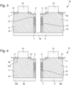
- embodiments of the present disclosure provide a semiconductor wafer comprising a plurality of chips and a separation zone spacing the semiconductor chips from each other in this wafer, such a separation zone extending from a front face to an opposite backside face of this wafer, this separation zone includes a scribe line configured to be diced using plasma etching and an inlet area of this scribe line, the inlet being delimitated by free ends of plasma etch-resistant material layers extending each from a peripheral wall of a functional part of the corresponding chip into the scribe line by overlapping a top of a seal ring of this chip.
- circuit means either a single component or a multiplicity of components, either active or passive, that are connected together to provide a desired function.
- directional terms such as “on”, “over”, “top”, “bottom”, “left”, “right” are used with reference to the orientation of the Figure(s) being described. Because components of embodiments of the present invention can be positioned in a number of different orientations, the directional terminology is used for purposes of illustration only and is in no way limiting. When used in conjunction with layers of a semiconductor wafer or corresponding circuit or device in the semiconductor wafer, the directional terminology is intended to be construed broadly, and therefore should not be interpreted to preclude the presence of one or more intervening layers or other intervening image sensor features or elements. Thus, a given layer that is described herein as being formed on or formed over another layer may be separated from the latter layer by one or more additional layers.
- This wafer 1a, 1b comprises a plurality of semiconductor chips 2, which can be in some embodiments, RFID chips, NFC chips or Bluetooth chips.
- this plurality of chips 2 is spaced from each other by a separation zone 3.
- the wafer 1a, 1b also comprises a chip carrier substrate 5 providing mechanical support, so that the wafer 1a, 1b does not break in the formation of structures constituting notably the plurality of chips 2.
- This carrier substrate 5 may be a blank silicon wafer 1a, 1b including no circuits formed therein in accordance with some exemplary embodiments.
- This carrier substrate 5 includes a backside face 4b of this wafer 1a, 1b and extending horizontally in the wafer 1a, 1b and more specifically into the plurality of chips 2 and the separation zone 3. As we will see later, this carrier substrate 5 is configured in particular to be diced by plasma etching.
- the wafer 1a, 1b includes a front face 4a formed by the top of this wafer 1a, 1b, and also the backside face 4b formed by the base of the carrier substrate 5 as mentioned earlier.
- each chip 2 of the wafer 1a, 1b includes a functional part 18 also called "active part".
- This functional part 18 including integrated circuits, is built on a part of the carrier substrate 5. Due to this, the chip 2 is essentially formed by this functional part 18 and the part of the substrate 5 on which it is built.
- each chip 2 comprises an upper surface 12a formed by the top of the functional part 18, and also a lower surface 12b formed by the base of the corresponding part of the carrier substrate 5. It can be noted that these upper and lower surfaces 12a, 12b are contained respectively in the front and backside faces 4a, 4b of the wafer 1a, 1b.
- each chip 2 includes a seal ring 7 forming a solid metal ring adjacent to a peripheral wall 20 of the functional part 18, so that moisture and detrimental chemicals may not penetrate into this chip 2 and reach an interconnected metal components 15 within this seal ring 7.
- the interconnected metal components 15 made of metal lines and conductive vias, both formed in dielectric layers. The metal lines and vias are physically connected.
- This seal ring 7 extends vertically in the chip 2 perpendicular or significantly perpendicular to the carrier substrate 5. In the wafer 1a, 1b, the seal ring 7s are disposed along the separation zone 3.
- each chip 2 also comprises at least one bump 14 protruding from its upper surface 12a formed by the top of its functional part 18.
- This bump 14 is made up of a stack of several layers of different materials such as layers of gold, copper and nickel.
- the bump 14 is preferably resistant to plasma etching. As we will see later, such bump 14 contributes to block the plasma etching in the wafer 1a, 1b.
- the wafer 1a, 1b includes the separation zone 3 spacing the chips 2 from each other.
- the separation zone 3 extends from the front face 4a to the backside face 4b of this wafer 1a, 1b.
- This separation zone 3 formed between the chips 2 may provide a mechanism for separating/extracting the chips 2 from the wafer 1a, 1b.
- this separation zone 3 includes a scribe line 6 located between the seal rings 7 of neighboring chips 2.
- both side walls of this scribe line 6 are in contact with these seal rings 7.
- both side walls are in contact or comprise parts of peripheral walls 20 of the chips located over the tops of the seal rings 7.
- these parts of the peripheral walls 20 are located between the tops of the seal rings 7 and the front face 4a of the wafer 1a, 1b.
- Such a scribe line 6 (also known as kerf or frame) is an area in the wafer 1a, 1b, which is configured to separate individual chip 2 at the end of wafer 1a, 1b processing.
- the scribe line 6 contains a material stack configured to be diced using plasma etching, this material stack being built on a corresponding part of the carrier substrate 5 of the wafer 1a, 1b.
- This material stack which is preferably an oxide stack, extends from the part of the carrier substrate 5 to the front face 4a of the wafer 1a, 1b. It can be noted that the top of this material stack forms an upper surface of the scribe line 6.
- the separation zone 3 comprises:
- Such plasma etch-resistant material layers 9 contribute to block the plasma etching in the wafer 1a, 1b.
- these layers are arranged in the wafer 1a, 1b for delimiting the inlet area 13 which gives access to the oxide stack contained in the scribe line 6.
- Each plasma etch-resistant material layer 9 extends from a peripheral wall 20 of a functional part 18 of a chip 2 into the scribe line 6.
- this plasma etch-resistant material layer 9 is a part of this functional part 18.
- each chip 2 includes this layer 9, which helps to form the inlet area 13 in the wafer.
- This plasma etch-resistant material layer 9 is formed by two parts. A first part comprising a free end of this layer 9 and which is localised in the scribe line 6 of the separation zone 3 and a second part which is completely included in this functional part 18. In this configuration, the first part protrudes from the peripheral wall 20 of the functional part 18 of each chip 2 into the scribe line 6:
- each plasma etch-resistant material layer 9 is included both in the functional part 18 of the chip 2 and in the material stack of the scribe line 6 located in the immediate vicinity of this chip 2.
- This layer 9 extends from an upper part 16 of the peripheral wall 20 of the functional part 18 of the chip 2 to an adjoining upper part 17 of a lateral zone of the scribe line 6 by being arranged above the top of the seal ring 7 that is to say a top layer of this seal ring 7.
- the second part of the plasma etch-resistant material layer 9 is comprised in this upper part 16 of the peripheral wall 20 of the functional part 18 of each chip 2.
- the first part of the plasma etch-resistant material layer 9 it is comprised in the upper part 17. It can be noted that this upper part 16 of the peripheral wall 20 of the functional part 18 of the chip 2 and the upper part 17 of the lateral zone of the scribe line 6 are joined together at the peripheral wall 20 of the chip 2.
- this layer extends in this volume while being parallel or substantially parallel to the carrier substrate 5 and/or perpendicular or substantially perpendicular to the seal ring 7.
- this layer extends in this volume while being perpendicular or substantially perpendicular to the peripheral wall 20 of the chip 2 to which it is attached.
- such a plasma etch-resistant material layer 9 is positioned between the front face 4a of the wafer 1a, 1b and the top layer of the seal ring 7.
- this layer 9 is located under both the upper surfaces 12a of the functional part 18/chip 2 and the scribe line 6 formed by the upper surface 19 of the top of the material stack (e.g. the oxide stack), and the top layer of the seal ring 7. It can be understood that in this configuration this layer by extending from the functional part 18 of the chip 2 to the material stack comprised in the scribe line 6, overlaps the top layer of the seal ring 7 of this chip 2.
- the plasma etch-resistant material layer 9 of each chip 2 is set up to cooperate with the plasma etch-resistant material layers 9 of its neighboring chips 2 in order to define the inlet area 13 of the separation zone 3 more specifically the inlet area 13 of the scribe line 6.
- the plasma etch-resistant material layer 9 of each chip 2 comprises a free end which is able to cooperate with the free ends of the plasma etch-resistant material layers 9 of its neighboring chips 2 in order to delimitate this inlet area 13.
- the plasma etch-resistant material layer 9 includes an upper face which is localised in the scribe line 6 under the front face 4a of the wafer 1a, 1b.
- this upper face can comprise a part of this front face 4a of the wafer 1a, 1b such a part being located in the upper part 16 of the peripheral wall 20 of the functional part 18 of the chip 2 and also in the said upper 17 part of the lateral zone of the scribe line 6.
- the upper face of this layer 9 forms a part of the front face 4a of the wafer 1a, 1b located in the upper part 16 of the peripheral wall 20 of the functional part 18 of the chip 2 and also in the said upper part 17 of the lateral zone of the scribe line 6.
- this layer of material resistant 9 comprises also a lower face opposite to the upper face. This lower face overlaps the top layer of the seal ring 7 of the chip 2 by being arranged facing this top layer more particularly by being located above this top layer. It can be noted that in this configuration, the layer of material resistant 9 is not connected to the interconnected metal components 15 arranged within seal ring 7. This positioning of that layer of material resistant 9 relatively to the top layer of the seal ring 7, allows to limit electrical perturbation from the environment/outside. Indeed, the seal ring 7 could be accessible from external electrostatic aggressions.
- the lower face of this layer of material resistant 9 is connected to the interconnected metal components 15 of the seal ring 7.
- This second embodiment offers the advantage regarding the first embodiment that the seal ring 7 can include more metal lines.
- the separation zone 3 also comprises a passivation layer 8 covering the inlet area 13 or sealing/closing the inlet area 13. More specifically, this passivation layer 8 covers a part of the upper faces of the plasma etch-resistant material layers 9 that delineated/defined that inlet area 13. That is, this passivation layer 8 covers a part of the upper faces of the plasma etch-resistant material layers 9 of the chips 2 that are close to each other. This part of this layer 9 which is covered by the passivation layer 8 being preferably includes in the said upper part 17 of lateral zone of the scribe line 6. Moreover, this passivation layer 8 also covers the material stack constituting the scribe line 6 more specifically the top of this material stack forming the upper surface 19 of the scribe line 6.
- the passivation layer 8 hermetically seals the inlet area 13 of the scribe line 6. In other words, this passivation layer 8 hermetically links together the free ends of plasma etch-resistant material layers 9 of the chips 2. It can be noted that the passivation layer 8 has a width W1 which is less than:
- the wafer 1a, 1b also comprises a passivation layer 11 covering the part of the upper surface 12a of each chip 2 which is exposed to the environment.
- these passivation layers 8, 11 need to have good adhesion, also during stressing, they are usually chemically inert, corrosion-resistant dielectrics (acting as diffusion barriers to water diffusion) and with wide bandgap (and thus high electrical breakdown strength). It is therefore in general Al2O3, SiO2, Si3N4, etc...
- the wafer 1a, 1b includes a layer of material partially resistant 10 to plasma etching covering the passivation layer 11 arranged over the part of the upper surface 12a of each chip 2 exposed to the environment.
- This layer of material partially resistant 10 to plasma etching is preferably a layer of polyimide. It can be noted that the passivation layer 11 and this layer of material partially resistant 10 to plasma etching encircle the base of each bump 14 of the chip 2. Such layer of material partially resistant 10 contributes to block the plasma etching in the wafer 1a, 1b.
- the plasma etch-resistant material layers 9, the layers of passivation 8, 11, the layers of material partially resistant 10 to plasma etching are formed during wafer 1a, 1b fabrication. Furthermore, the passivation layer 8, the plasma etch-resistant material layer 9 and the layer of material partially resistant 10 are preferably made from different materials.
- an operation for separating the wafer 1a, 1b into a plurality of semiconductor chips 2 is illustrated. This operation implements notably two etching processes performed on the wafer 1a, 1b.
- a first etching process has been performed on the wafer 1a, 1b in order to etch the material stack and the passivation layer 8 which covered it.
- This material stack and the passivation layer 8 contained in the separation zone 3, are configured to be diced using plasma etching.
- This first etching process comprises the implementation of a plasma oxide etching when that material stack is an oxide stack. It may be noted that during this plasma oxide etching, the wafer 1a, 1b - more particularly the plurality of chips 2 - is protected against the plasma oxide attacks by the at least one bump 14, the layers of material partially resistant 10 to plasma etching here the layers of polyimide and the plasma etch-resistant material layers 9 here the layers of aluminium.
- the passivation layer 8 covering the inlet area 13 which is not protected by the layer of polyimide is fully etched until the plasma reaches the layers of aluminium. Moreover, once this passivation layer 8 has been etched, the plasma enters into the scribe line 6 through the inlet area 13 and etches the oxide stack contained in this scribe line 6 until the carrier substrate 5. In this set up, the etching speed is similar for the layer of polyimide and the oxide stack in the scribe line 6 because the layer of polyimide has been chosen to be thicker than the oxide stack.
- the layer of aluminium is partially exposed to the environment and more particularly to the ambient air.
- the metal lines of the interconnected metal components 15 within seal ring 7 of each chip 2 are covered by the remaining oxide comprised in the lateral zones of the scribe line 6. Indeed all the external part of the seal ring 7 already covered by the oxide stack comprised in the scribe line 6, is covered by this remaining oxide.
- This remaining oxide results from the arrangement of the plasma etch-resistant material layer 9 relative to the top layer of the seal ring 7. Indeed, for each chip 2, the plasma etch-resistant material layer 9 is overlapping this top layer of the seal ring 7. In other word, the overlapping of this top layer by plasma etch-resistant material layer 9 is configured to maintain the metal lines covered by the remaining oxide. Consequently, the metal lines are protected against external moisture.
- the remaining layers of polyimide are thinner than before the starting of the first etching process.
- this second etching process sets out the implementation of a plasma silicon etching when the layer of material constituting this substrate 5 is a layer of silicon.
- each plasma etch-resistant material layer 9 stays attached to the chip 2 after the operation for separating the wafer 1a, 1b into a plurality of semiconductor chips 2. Under these circumstances, this layer can be considered as forming part of this chip 2.
- such wafer 1a, 1b contributes to optimize the number of chips 2 per wafer 1a, 1b and hence the product cost by reducing the width of the separation zone 3 and more specifically of the inlet area 13 of the scribe line 6.
- this width of the inlet area 13 is comprised between 3 and 10 ⁇ m, and preferably 5 ⁇ m.
- such a wafer 1a, 1b contributes to improve the execution of the operation for separating the wafer 1a, 1b into a plurality of semiconductor chips 2 compared to wafers in the prior art, and that especially when semiconductor chips 2 have small or even tiny dimensions.
Landscapes
- Dicing (AREA)
Applications Claiming Priority (1)
| Application Number | Priority Date | Filing Date | Title |
|---|---|---|---|
| EP22194854 | 2022-09-09 |
Publications (1)
| Publication Number | Publication Date |
|---|---|
| EP4336548A1 true EP4336548A1 (de) | 2024-03-13 |
Family
ID=83271212
Family Applications (1)
| Application Number | Title | Priority Date | Filing Date |
|---|---|---|---|
| EP23196392.7A Pending EP4336548A1 (de) | 2022-09-09 | 2023-09-08 | Halbleiterscheibe |
Country Status (2)
| Country | Link |
|---|---|
| US (1) | US20240088066A1 (de) |
| EP (1) | EP4336548A1 (de) |
Citations (7)
| Publication number | Priority date | Publication date | Assignee | Title |
|---|---|---|---|---|
| US20030122220A1 (en) * | 1999-05-20 | 2003-07-03 | West Jeffrey A. | Scribe street seals in semiconductor devices and method of fabrication |
| US20050269702A1 (en) * | 2003-04-30 | 2005-12-08 | Fujitsu Limited | Method for fabricating semiconductor device capable of scribing chips with high yield |
| US20140167226A1 (en) * | 2007-11-12 | 2014-06-19 | Infineon Technologies Ag | Wafer and a Method of Dicing a Wafer |
| US20170256638A1 (en) * | 2016-03-03 | 2017-09-07 | Gan Systems Inc. | GaN-on-Si SEMICONDUCTOR DEVICE STRUCTURES FOR HIGH CURRENT/ HIGH VOLTAGE LATERAL GaN TRANSISTORS AND METHODS OF FABRICATION THEREOF |
| WO2018063642A2 (en) * | 2016-09-30 | 2018-04-05 | Intel IP Corporation | Methods and structures for dicing integrated circuits from a wafer |
| CN107910295A (zh) * | 2017-12-27 | 2018-04-13 | 江阴长电先进封装有限公司 | 一种晶圆级芯片封装结构及其封装方法 |
| US20210193524A1 (en) * | 2019-12-19 | 2021-06-24 | Nxp B.V. | Method and System for Regulating Plasma Dicing Rates |
-
2023
- 2023-09-08 US US18/463,771 patent/US20240088066A1/en active Pending
- 2023-09-08 EP EP23196392.7A patent/EP4336548A1/de active Pending
Patent Citations (7)
| Publication number | Priority date | Publication date | Assignee | Title |
|---|---|---|---|---|
| US20030122220A1 (en) * | 1999-05-20 | 2003-07-03 | West Jeffrey A. | Scribe street seals in semiconductor devices and method of fabrication |
| US20050269702A1 (en) * | 2003-04-30 | 2005-12-08 | Fujitsu Limited | Method for fabricating semiconductor device capable of scribing chips with high yield |
| US20140167226A1 (en) * | 2007-11-12 | 2014-06-19 | Infineon Technologies Ag | Wafer and a Method of Dicing a Wafer |
| US20170256638A1 (en) * | 2016-03-03 | 2017-09-07 | Gan Systems Inc. | GaN-on-Si SEMICONDUCTOR DEVICE STRUCTURES FOR HIGH CURRENT/ HIGH VOLTAGE LATERAL GaN TRANSISTORS AND METHODS OF FABRICATION THEREOF |
| WO2018063642A2 (en) * | 2016-09-30 | 2018-04-05 | Intel IP Corporation | Methods and structures for dicing integrated circuits from a wafer |
| CN107910295A (zh) * | 2017-12-27 | 2018-04-13 | 江阴长电先进封装有限公司 | 一种晶圆级芯片封装结构及其封装方法 |
| US20210193524A1 (en) * | 2019-12-19 | 2021-06-24 | Nxp B.V. | Method and System for Regulating Plasma Dicing Rates |
Also Published As
| Publication number | Publication date |
|---|---|
| US20240088066A1 (en) | 2024-03-14 |
Similar Documents
| Publication | Publication Date | Title |
|---|---|---|
| US9305843B2 (en) | Chip package and method for forming the same | |
| US11069647B2 (en) | Semiconductor wafer, bonding structure and wafer bonding method | |
| US8643070B2 (en) | Chip package and method for forming the same | |
| US20120184070A1 (en) | Method for forming chip package | |
| US10930602B2 (en) | Semiconductor device and method for fabricating the same | |
| CN104952812A (zh) | 晶片封装体及其制造方法 | |
| US9640488B2 (en) | Chip package and method for forming the same | |
| US9024437B2 (en) | Chip package and method for forming the same | |
| US11276670B2 (en) | Semiconductor device and manufacturing method of semiconductor device | |
| US11174156B2 (en) | Bonding process for forming semiconductor device structure | |
| TWI539537B (zh) | 晶片封裝體及其製造方法 | |
| US20060160273A1 (en) | Method for wafer level packaging | |
| US8193640B2 (en) | MEMS and a protection structure thereof | |
| US20190067215A1 (en) | Trench structure and method | |
| EP4336548A1 (de) | Halbleiterscheibe | |
| CN102190281A (zh) | 芯片封装体及其形成方法 | |
| CN219885672U (zh) | 一种半导体晶圆以及管芯 | |
| CN113517205A (zh) | 半导体器件及其形成方法 | |
| US20070029631A1 (en) | Package Structure and Wafer Level Package Method | |
| US12500149B2 (en) | Semiconductor device and method of forming the same | |
| TWI482548B (zh) | 線路結構的製造方法 | |
| US20230326882A1 (en) | Semiconductor structure and manufacturing method thereof | |
| KR101013547B1 (ko) | 웨이퍼 레벨 칩 사이즈 패키지의 제조 방법 | |
| US10777461B2 (en) | Method for manufacturing a chip package |
Legal Events
| Date | Code | Title | Description |
|---|---|---|---|
| PUAI | Public reference made under article 153(3) epc to a published international application that has entered the european phase |
Free format text: ORIGINAL CODE: 0009012 |
|
| STAA | Information on the status of an ep patent application or granted ep patent |
Free format text: STATUS: THE APPLICATION HAS BEEN PUBLISHED |
|
| AK | Designated contracting states |
Kind code of ref document: A1 Designated state(s): AL AT BE BG CH CY CZ DE DK EE ES FI FR GB GR HR HU IE IS IT LI LT LU LV MC ME MK MT NL NO PL PT RO RS SE SI SK SM TR |
|
| STAA | Information on the status of an ep patent application or granted ep patent |
Free format text: STATUS: REQUEST FOR EXAMINATION WAS MADE |
|
| 17P | Request for examination filed |
Effective date: 20240912 |
|
| RBV | Designated contracting states (corrected) |
Designated state(s): AL AT BE BG CH CY CZ DE DK EE ES FI FR GB GR HR HU IE IS IT LI LT LU LV MC ME MK MT NL NO PL PT RO RS SE SI SK SM TR |
|
| P01 | Opt-out of the competence of the unified patent court (upc) registered |
Free format text: CASE NUMBER: APP_9433/2025 Effective date: 20250226 |