EP4335854A1 - Novel compound and organic light emitting device comprising the same - Google Patents
Novel compound and organic light emitting device comprising the same Download PDFInfo
- Publication number
- EP4335854A1 EP4335854A1 EP22870131.4A EP22870131A EP4335854A1 EP 4335854 A1 EP4335854 A1 EP 4335854A1 EP 22870131 A EP22870131 A EP 22870131A EP 4335854 A1 EP4335854 A1 EP 4335854A1
- Authority
- EP
- European Patent Office
- Prior art keywords
- compound
- group
- light emitting
- substituted
- chemical formula
- Prior art date
- Legal status (The legal status is an assumption and is not a legal conclusion. Google has not performed a legal analysis and makes no representation as to the accuracy of the status listed.)
- Pending
Links
- 150000001875 compounds Chemical class 0.000 title claims abstract description 180
- 239000000126 substance Substances 0.000 claims description 44
- 239000011368 organic material Substances 0.000 claims description 38
- 125000003118 aryl group Chemical group 0.000 claims description 25
- 125000001424 substituent group Chemical group 0.000 claims description 24
- YZCKVEUIGOORGS-OUBTZVSYSA-N Deuterium Chemical group [2H] YZCKVEUIGOORGS-OUBTZVSYSA-N 0.000 claims description 17
- 125000000217 alkyl group Chemical group 0.000 claims description 17
- 229910052805 deuterium Inorganic materials 0.000 claims description 17
- 150000002431 hydrogen Chemical group 0.000 claims description 16
- 229910052739 hydrogen Inorganic materials 0.000 claims description 16
- 239000001257 hydrogen Substances 0.000 claims description 16
- 125000001997 phenyl group Chemical group [H]C1=C([H])C([H])=C(*)C([H])=C1[H] 0.000 claims description 16
- 125000000999 tert-butyl group Chemical group [H]C([H])([H])C(*)(C([H])([H])[H])C([H])([H])[H] 0.000 claims description 15
- 125000000753 cycloalkyl group Chemical group 0.000 claims description 9
- UHOVQNZJYSORNB-UHFFFAOYSA-N monobenzene Natural products C1=CC=CC=C1 UHOVQNZJYSORNB-UHFFFAOYSA-N 0.000 claims description 8
- FCEHBMOGCRZNNI-UHFFFAOYSA-N 1-benzothiophene Chemical compound C1=CC=C2SC=CC2=C1 FCEHBMOGCRZNNI-UHFFFAOYSA-N 0.000 claims description 5
- 229910052760 oxygen Inorganic materials 0.000 claims description 5
- 125000006713 (C5-C10) cycloalkyl group Chemical group 0.000 claims description 4
- 229910052757 nitrogen Inorganic materials 0.000 claims description 4
- 229910052717 sulfur Inorganic materials 0.000 claims description 4
- 125000000113 cyclohexyl group Chemical group [H]C1([H])C([H])([H])C([H])([H])C([H])(*)C([H])([H])C1([H])[H] 0.000 claims description 3
- 125000005842 heteroatom Chemical group 0.000 claims description 3
- 125000001449 isopropyl group Chemical group [H]C([H])([H])C([H])(*)C([H])([H])[H] 0.000 claims description 3
- 125000002496 methyl group Chemical group [H]C([H])([H])* 0.000 claims description 3
- 125000006819 (C2-60) heteroaryl group Chemical group 0.000 claims description 2
- 125000006376 (C3-C10) cycloalkyl group Chemical group 0.000 claims description 2
- 125000005073 adamantyl group Chemical group C12(CC3CC(CC(C1)C3)C2)* 0.000 claims description 2
- 125000002947 alkylene group Chemical group 0.000 claims description 2
- 239000010410 layer Substances 0.000 description 101
- YMWUJEATGCHHMB-UHFFFAOYSA-N Dichloromethane Chemical compound ClCCl YMWUJEATGCHHMB-UHFFFAOYSA-N 0.000 description 83
- 238000002360 preparation method Methods 0.000 description 48
- -1 triethylsilyl group Chemical group 0.000 description 46
- CSNNHWWHGAXBCP-UHFFFAOYSA-L Magnesium sulfate Chemical compound [Mg+2].[O-][S+2]([O-])([O-])[O-] CSNNHWWHGAXBCP-UHFFFAOYSA-L 0.000 description 40
- 239000000243 solution Substances 0.000 description 38
- 238000006243 chemical reaction Methods 0.000 description 30
- 239000000463 material Substances 0.000 description 30
- XLYOFNOQVPJJNP-UHFFFAOYSA-N water Substances O XLYOFNOQVPJJNP-UHFFFAOYSA-N 0.000 description 30
- 238000002347 injection Methods 0.000 description 29
- 239000007924 injection Substances 0.000 description 29
- 239000011541 reaction mixture Substances 0.000 description 25
- 238000000034 method Methods 0.000 description 23
- 239000012044 organic layer Substances 0.000 description 21
- 238000004440 column chromatography Methods 0.000 description 20
- 229910052943 magnesium sulfate Inorganic materials 0.000 description 20
- 239000000203 mixture Substances 0.000 description 20
- 239000000377 silicon dioxide Substances 0.000 description 20
- VYPSYNLAJGMNEJ-UHFFFAOYSA-N silicon dioxide Inorganic materials O=[Si]=O VYPSYNLAJGMNEJ-UHFFFAOYSA-N 0.000 description 20
- OKTJSMMVPCPJKN-UHFFFAOYSA-N Carbon Chemical compound [C] OKTJSMMVPCPJKN-UHFFFAOYSA-N 0.000 description 18
- 229910052799 carbon Inorganic materials 0.000 description 18
- 239000008199 coating composition Substances 0.000 description 16
- 239000012267 brine Substances 0.000 description 15
- HPALAKNZSZLMCH-UHFFFAOYSA-M sodium;chloride;hydrate Chemical compound O.[Na+].[Cl-] HPALAKNZSZLMCH-UHFFFAOYSA-M 0.000 description 15
- 230000032258 transport Effects 0.000 description 15
- MXQOYLRVSVOCQT-UHFFFAOYSA-N bis(tri-t-butylphosphine)palladium (0) Substances [Pd].CC(C)(C)P(C(C)(C)C)C(C)(C)C.CC(C)(C)P(C(C)(C)C)C(C)(C)C MXQOYLRVSVOCQT-UHFFFAOYSA-N 0.000 description 13
- MFRIHAYPQRLWNB-UHFFFAOYSA-N sodium tert-butoxide Chemical compound [Na+].CC(C)(C)[O-] MFRIHAYPQRLWNB-UHFFFAOYSA-N 0.000 description 13
- 239000002904 solvent Substances 0.000 description 13
- 239000000758 substrate Substances 0.000 description 13
- 230000005525 hole transport Effects 0.000 description 11
- 230000000052 comparative effect Effects 0.000 description 10
- 229940125904 compound 1 Drugs 0.000 description 10
- 125000000623 heterocyclic group Chemical group 0.000 description 10
- 239000002096 quantum dot Substances 0.000 description 8
- 125000003342 alkenyl group Chemical group 0.000 description 7
- CSCPPACGZOOCGX-UHFFFAOYSA-N Acetone Chemical compound CC(C)=O CSCPPACGZOOCGX-UHFFFAOYSA-N 0.000 description 6
- OKKJLVBELUTLKV-UHFFFAOYSA-N Methanol Chemical compound OC OKKJLVBELUTLKV-UHFFFAOYSA-N 0.000 description 6
- WYURNTSHIVDZCO-UHFFFAOYSA-N Tetrahydrofuran Chemical compound C1CCOC1 WYURNTSHIVDZCO-UHFFFAOYSA-N 0.000 description 6
- YXFVVABEGXRONW-UHFFFAOYSA-N Toluene Chemical compound CC1=CC=CC=C1 YXFVVABEGXRONW-UHFFFAOYSA-N 0.000 description 6
- 229910052782 aluminium Inorganic materials 0.000 description 6
- XAGFODPZIPBFFR-UHFFFAOYSA-N aluminium Chemical compound [Al] XAGFODPZIPBFFR-UHFFFAOYSA-N 0.000 description 6
- JHIVVAPYMSGYDF-UHFFFAOYSA-N cyclohexanone Chemical compound O=C1CCCCC1 JHIVVAPYMSGYDF-UHFFFAOYSA-N 0.000 description 6
- 239000002019 doping agent Substances 0.000 description 6
- AOSZTAHDEDLTLQ-AZKQZHLXSA-N (1S,2S,4R,8S,9S,11S,12R,13S,19S)-6-[(3-chlorophenyl)methyl]-12,19-difluoro-11-hydroxy-8-(2-hydroxyacetyl)-9,13-dimethyl-6-azapentacyclo[10.8.0.02,9.04,8.013,18]icosa-14,17-dien-16-one Chemical compound C([C@@H]1C[C@H]2[C@H]3[C@]([C@]4(C=CC(=O)C=C4[C@@H](F)C3)C)(F)[C@@H](O)C[C@@]2([C@@]1(C1)C(=O)CO)C)N1CC1=CC=CC(Cl)=C1 AOSZTAHDEDLTLQ-AZKQZHLXSA-N 0.000 description 5
- QFLWZFQWSBQYPS-AWRAUJHKSA-N (3S)-3-[[(2S)-2-[[(2S)-2-[5-[(3aS,6aR)-2-oxo-1,3,3a,4,6,6a-hexahydrothieno[3,4-d]imidazol-4-yl]pentanoylamino]-3-methylbutanoyl]amino]-3-(4-hydroxyphenyl)propanoyl]amino]-4-[1-bis(4-chlorophenoxy)phosphorylbutylamino]-4-oxobutanoic acid Chemical compound CCCC(NC(=O)[C@H](CC(O)=O)NC(=O)[C@H](Cc1ccc(O)cc1)NC(=O)[C@@H](NC(=O)CCCCC1SC[C@@H]2NC(=O)N[C@H]12)C(C)C)P(=O)(Oc1ccc(Cl)cc1)Oc1ccc(Cl)cc1 QFLWZFQWSBQYPS-AWRAUJHKSA-N 0.000 description 5
- 229940126657 Compound 17 Drugs 0.000 description 5
- KFZMGEQAYNKOFK-UHFFFAOYSA-N Isopropanol Chemical compound CC(C)O KFZMGEQAYNKOFK-UHFFFAOYSA-N 0.000 description 5
- 150000004982 aromatic amines Chemical class 0.000 description 5
- 238000000151 deposition Methods 0.000 description 5
- 239000012153 distilled water Substances 0.000 description 5
- 229910052751 metal Inorganic materials 0.000 description 5
- 239000002184 metal Substances 0.000 description 5
- AKHNMLFCWUSKQB-UHFFFAOYSA-L sodium thiosulfate Chemical compound [Na+].[Na+].[O-]S([O-])(=O)=S AKHNMLFCWUSKQB-UHFFFAOYSA-L 0.000 description 5
- GLGNXYJARSMNGJ-VKTIVEEGSA-N (1s,2s,3r,4r)-3-[[5-chloro-2-[(1-ethyl-6-methoxy-2-oxo-4,5-dihydro-3h-1-benzazepin-7-yl)amino]pyrimidin-4-yl]amino]bicyclo[2.2.1]hept-5-ene-2-carboxamide Chemical compound CCN1C(=O)CCCC2=C(OC)C(NC=3N=C(C(=CN=3)Cl)N[C@H]3[C@H]([C@@]4([H])C[C@@]3(C=C4)[H])C(N)=O)=CC=C21 GLGNXYJARSMNGJ-VKTIVEEGSA-N 0.000 description 4
- OPFJDXRVMFKJJO-ZHHKINOHSA-N N-{[3-(2-benzamido-4-methyl-1,3-thiazol-5-yl)-pyrazol-5-yl]carbonyl}-G-dR-G-dD-dD-dD-NH2 Chemical compound S1C(C=2NN=C(C=2)C(=O)NCC(=O)N[C@H](CCCN=C(N)N)C(=O)NCC(=O)N[C@H](CC(O)=O)C(=O)N[C@H](CC(O)=O)C(=O)N[C@H](CC(O)=O)C(N)=O)=C(C)N=C1NC(=O)C1=CC=CC=C1 OPFJDXRVMFKJJO-ZHHKINOHSA-N 0.000 description 4
- 239000000956 alloy Substances 0.000 description 4
- 229910045601 alloy Inorganic materials 0.000 description 4
- 239000010405 anode material Substances 0.000 description 4
- 239000011248 coating agent Substances 0.000 description 4
- 238000000576 coating method Methods 0.000 description 4
- 229940125758 compound 15 Drugs 0.000 description 4
- 229940126086 compound 21 Drugs 0.000 description 4
- 125000004185 ester group Chemical group 0.000 description 4
- 238000010438 heat treatment Methods 0.000 description 4
- BWHMMNNQKKPAPP-UHFFFAOYSA-L potassium carbonate Chemical compound [K+].[K+].[O-]C([O-])=O BWHMMNNQKKPAPP-UHFFFAOYSA-L 0.000 description 4
- SZUVGFMDDVSKSI-WIFOCOSTSA-N (1s,2s,3s,5r)-1-(carboxymethyl)-3,5-bis[(4-phenoxyphenyl)methyl-propylcarbamoyl]cyclopentane-1,2-dicarboxylic acid Chemical compound O=C([C@@H]1[C@@H]([C@](CC(O)=O)([C@H](C(=O)N(CCC)CC=2C=CC(OC=3C=CC=CC=3)=CC=2)C1)C(O)=O)C(O)=O)N(CCC)CC(C=C1)=CC=C1OC1=CC=CC=C1 SZUVGFMDDVSKSI-WIFOCOSTSA-N 0.000 description 3
- GHYOCDFICYLMRF-UTIIJYGPSA-N (2S,3R)-N-[(2S)-3-(cyclopenten-1-yl)-1-[(2R)-2-methyloxiran-2-yl]-1-oxopropan-2-yl]-3-hydroxy-3-(4-methoxyphenyl)-2-[[(2S)-2-[(2-morpholin-4-ylacetyl)amino]propanoyl]amino]propanamide Chemical compound C1(=CCCC1)C[C@@H](C(=O)[C@@]1(OC1)C)NC([C@H]([C@@H](C1=CC=C(C=C1)OC)O)NC([C@H](C)NC(CN1CCOCC1)=O)=O)=O GHYOCDFICYLMRF-UTIIJYGPSA-N 0.000 description 3
- WWTBZEKOSBFBEM-SPWPXUSOSA-N (2s)-2-[[2-benzyl-3-[hydroxy-[(1r)-2-phenyl-1-(phenylmethoxycarbonylamino)ethyl]phosphoryl]propanoyl]amino]-3-(1h-indol-3-yl)propanoic acid Chemical compound N([C@@H](CC=1C2=CC=CC=C2NC=1)C(=O)O)C(=O)C(CP(O)(=O)[C@H](CC=1C=CC=CC=1)NC(=O)OCC=1C=CC=CC=1)CC1=CC=CC=C1 WWTBZEKOSBFBEM-SPWPXUSOSA-N 0.000 description 3
- IWZSHWBGHQBIML-ZGGLMWTQSA-N (3S,8S,10R,13S,14S,17S)-17-isoquinolin-7-yl-N,N,10,13-tetramethyl-2,3,4,7,8,9,11,12,14,15,16,17-dodecahydro-1H-cyclopenta[a]phenanthren-3-amine Chemical compound CN(C)[C@H]1CC[C@]2(C)C3CC[C@@]4(C)[C@@H](CC[C@@H]4c4ccc5ccncc5c4)[C@@H]3CC=C2C1 IWZSHWBGHQBIML-ZGGLMWTQSA-N 0.000 description 3
- ONBQEOIKXPHGMB-VBSBHUPXSA-N 1-[2-[(2s,3r,4s,5r)-3,4-dihydroxy-5-(hydroxymethyl)oxolan-2-yl]oxy-4,6-dihydroxyphenyl]-3-(4-hydroxyphenyl)propan-1-one Chemical compound O[C@@H]1[C@H](O)[C@@H](CO)O[C@H]1OC1=CC(O)=CC(O)=C1C(=O)CCC1=CC=C(O)C=C1 ONBQEOIKXPHGMB-VBSBHUPXSA-N 0.000 description 3
- UNILWMWFPHPYOR-KXEYIPSPSA-M 1-[6-[2-[3-[3-[3-[2-[2-[3-[[2-[2-[[(2r)-1-[[2-[[(2r)-1-[3-[2-[2-[3-[[2-(2-amino-2-oxoethoxy)acetyl]amino]propoxy]ethoxy]ethoxy]propylamino]-3-hydroxy-1-oxopropan-2-yl]amino]-2-oxoethyl]amino]-3-[(2r)-2,3-di(hexadecanoyloxy)propyl]sulfanyl-1-oxopropan-2-yl Chemical compound O=C1C(SCCC(=O)NCCCOCCOCCOCCCNC(=O)COCC(=O)N[C@@H](CSC[C@@H](COC(=O)CCCCCCCCCCCCCCC)OC(=O)CCCCCCCCCCCCCCC)C(=O)NCC(=O)N[C@H](CO)C(=O)NCCCOCCOCCOCCCNC(=O)COCC(N)=O)CC(=O)N1CCNC(=O)CCCCCN\1C2=CC=C(S([O-])(=O)=O)C=C2CC/1=C/C=C/C=C/C1=[N+](CC)C2=CC=C(S([O-])(=O)=O)C=C2C1 UNILWMWFPHPYOR-KXEYIPSPSA-M 0.000 description 3
- ZWEHNKRNPOVVGH-UHFFFAOYSA-N 2-Butanone Chemical compound CCC(C)=O ZWEHNKRNPOVVGH-UHFFFAOYSA-N 0.000 description 3
- ZOXJGFHDIHLPTG-UHFFFAOYSA-N Boron Chemical group [B] ZOXJGFHDIHLPTG-UHFFFAOYSA-N 0.000 description 3
- XEKOWRVHYACXOJ-UHFFFAOYSA-N Ethyl acetate Chemical compound CCOC(C)=O XEKOWRVHYACXOJ-UHFFFAOYSA-N 0.000 description 3
- LYCAIKOWRPUZTN-UHFFFAOYSA-N Ethylene glycol Chemical compound OCCO LYCAIKOWRPUZTN-UHFFFAOYSA-N 0.000 description 3
- GYHNNYVSQQEPJS-UHFFFAOYSA-N Gallium Chemical compound [Ga] GYHNNYVSQQEPJS-UHFFFAOYSA-N 0.000 description 3
- ZMXDDKWLCZADIW-UHFFFAOYSA-N N,N-Dimethylformamide Chemical compound CN(C)C=O ZMXDDKWLCZADIW-UHFFFAOYSA-N 0.000 description 3
- IMNFDUFMRHMDMM-UHFFFAOYSA-N N-Heptane Chemical compound CCCCCCC IMNFDUFMRHMDMM-UHFFFAOYSA-N 0.000 description 3
- DNIAPMSPPWPWGF-UHFFFAOYSA-N Propylene glycol Chemical compound CC(O)CO DNIAPMSPPWPWGF-UHFFFAOYSA-N 0.000 description 3
- YTPLMLYBLZKORZ-UHFFFAOYSA-N Thiophene Chemical group C=1C=CSC=1 YTPLMLYBLZKORZ-UHFFFAOYSA-N 0.000 description 3
- LNUFLCYMSVYYNW-ZPJMAFJPSA-N [(2r,3r,4s,5r,6r)-2-[(2r,3r,4s,5r,6r)-6-[(2r,3r,4s,5r,6r)-6-[(2r,3r,4s,5r,6r)-6-[[(3s,5s,8r,9s,10s,13r,14s,17r)-10,13-dimethyl-17-[(2r)-6-methylheptan-2-yl]-2,3,4,5,6,7,8,9,11,12,14,15,16,17-tetradecahydro-1h-cyclopenta[a]phenanthren-3-yl]oxy]-4,5-disulfo Chemical compound O([C@@H]1[C@@H](COS(O)(=O)=O)O[C@@H]([C@@H]([C@H]1OS(O)(=O)=O)OS(O)(=O)=O)O[C@@H]1[C@@H](COS(O)(=O)=O)O[C@@H]([C@@H]([C@H]1OS(O)(=O)=O)OS(O)(=O)=O)O[C@@H]1[C@@H](COS(O)(=O)=O)O[C@H]([C@@H]([C@H]1OS(O)(=O)=O)OS(O)(=O)=O)O[C@@H]1C[C@@H]2CC[C@H]3[C@@H]4CC[C@@H]([C@]4(CC[C@@H]3[C@@]2(C)CC1)C)[C@H](C)CCCC(C)C)[C@H]1O[C@H](COS(O)(=O)=O)[C@@H](OS(O)(=O)=O)[C@H](OS(O)(=O)=O)[C@H]1OS(O)(=O)=O LNUFLCYMSVYYNW-ZPJMAFJPSA-N 0.000 description 3
- 125000002877 alkyl aryl group Chemical group 0.000 description 3
- 125000003277 amino group Chemical group 0.000 description 3
- 125000003710 aryl alkyl group Chemical group 0.000 description 3
- 125000001769 aryl amino group Chemical group 0.000 description 3
- 125000006267 biphenyl group Chemical group 0.000 description 3
- 125000002915 carbonyl group Chemical group [*:2]C([*:1])=O 0.000 description 3
- 239000010406 cathode material Substances 0.000 description 3
- 229940125773 compound 10 Drugs 0.000 description 3
- 229940125797 compound 12 Drugs 0.000 description 3
- 229940126543 compound 14 Drugs 0.000 description 3
- 229940126142 compound 16 Drugs 0.000 description 3
- 229940125782 compound 2 Drugs 0.000 description 3
- 229940125810 compound 20 Drugs 0.000 description 3
- 229940126208 compound 22 Drugs 0.000 description 3
- 229940126214 compound 3 Drugs 0.000 description 3
- 229940125898 compound 5 Drugs 0.000 description 3
- 230000000694 effects Effects 0.000 description 3
- 125000003983 fluorenyl group Chemical group C1(=CC=CC=2C3=CC=CC=C3CC12)* 0.000 description 3
- 229910052733 gallium Inorganic materials 0.000 description 3
- JAXFJECJQZDFJS-XHEPKHHKSA-N gtpl8555 Chemical compound OC(=O)C[C@H](N)C(=O)N[C@@H](CCC(O)=O)C(=O)N[C@@H](C(C)C)C(=O)N[C@@H](C(C)C)C(=O)N1CCC[C@@H]1C(=O)N[C@H](B1O[C@@]2(C)[C@H]3C[C@H](C3(C)C)C[C@H]2O1)CCC1=CC=C(F)C=C1 JAXFJECJQZDFJS-XHEPKHHKSA-N 0.000 description 3
- 238000004770 highest occupied molecular orbital Methods 0.000 description 3
- RAXXELZNTBOGNW-UHFFFAOYSA-N imidazole Natural products C1=CNC=N1 RAXXELZNTBOGNW-UHFFFAOYSA-N 0.000 description 3
- 125000005462 imide group Chemical group 0.000 description 3
- ZLVXBBHTMQJRSX-VMGNSXQWSA-N jdtic Chemical compound C1([C@]2(C)CCN(C[C@@H]2C)C[C@H](C(C)C)NC(=O)[C@@H]2NCC3=CC(O)=CC=C3C2)=CC=CC(O)=C1 ZLVXBBHTMQJRSX-VMGNSXQWSA-N 0.000 description 3
- 150000002739 metals Chemical class 0.000 description 3
- 125000003808 silyl group Chemical group [H][Si]([H])([H])[*] 0.000 description 3
- UBOXGVDOUJQMTN-UHFFFAOYSA-N 1,1,2-trichloroethane Chemical compound ClCC(Cl)Cl UBOXGVDOUJQMTN-UHFFFAOYSA-N 0.000 description 2
- FYGHSUNMUKGBRK-UHFFFAOYSA-N 1,2,3-trimethylbenzene Chemical compound CC1=CC=CC(C)=C1C FYGHSUNMUKGBRK-UHFFFAOYSA-N 0.000 description 2
- RFFLAFLAYFXFSW-UHFFFAOYSA-N 1,2-dichlorobenzene Chemical compound ClC1=CC=CC=C1Cl RFFLAFLAYFXFSW-UHFFFAOYSA-N 0.000 description 2
- 125000005916 2-methylpentyl group Chemical group 0.000 description 2
- XKRFYHLGVUSROY-UHFFFAOYSA-N Argon Chemical compound [Ar] XKRFYHLGVUSROY-UHFFFAOYSA-N 0.000 description 2
- IJGRMHOSHXDMSA-UHFFFAOYSA-N Atomic nitrogen Chemical compound N#N IJGRMHOSHXDMSA-UHFFFAOYSA-N 0.000 description 2
- ZAMOUSCENKQFHK-UHFFFAOYSA-N Chlorine atom Chemical compound [Cl] ZAMOUSCENKQFHK-UHFFFAOYSA-N 0.000 description 2
- HEDRZPFGACZZDS-UHFFFAOYSA-N Chloroform Chemical compound ClC(Cl)Cl HEDRZPFGACZZDS-UHFFFAOYSA-N 0.000 description 2
- IAZDPXIOMUYVGZ-UHFFFAOYSA-N Dimethylsulphoxide Chemical compound CS(C)=O IAZDPXIOMUYVGZ-UHFFFAOYSA-N 0.000 description 2
- LFQSCWFLJHTTHZ-UHFFFAOYSA-N Ethanol Chemical compound CCO LFQSCWFLJHTTHZ-UHFFFAOYSA-N 0.000 description 2
- YLQBMQCUIZJEEH-UHFFFAOYSA-N Furan Chemical group C=1C=COC=1 YLQBMQCUIZJEEH-UHFFFAOYSA-N 0.000 description 2
- PEDCQBHIVMGVHV-UHFFFAOYSA-N Glycerine Chemical compound OCC(O)CO PEDCQBHIVMGVHV-UHFFFAOYSA-N 0.000 description 2
- WHXSMMKQMYFTQS-UHFFFAOYSA-N Lithium Chemical compound [Li] WHXSMMKQMYFTQS-UHFFFAOYSA-N 0.000 description 2
- PFYHAAAQPNMZHO-UHFFFAOYSA-N Methyl 2-methoxybenzoate Chemical compound COC(=O)C1=CC=CC=C1OC PFYHAAAQPNMZHO-UHFFFAOYSA-N 0.000 description 2
- SECXISVLQFMRJM-UHFFFAOYSA-N N-Methylpyrrolidone Chemical compound CN1CCCC1=O SECXISVLQFMRJM-UHFFFAOYSA-N 0.000 description 2
- KDLHZDBZIXYQEI-UHFFFAOYSA-N Palladium Chemical compound [Pd] KDLHZDBZIXYQEI-UHFFFAOYSA-N 0.000 description 2
- NFHFRUOZVGFOOS-UHFFFAOYSA-N Pd(PPh3)4 Substances [Pd].C1=CC=CC=C1P(C=1C=CC=CC=1)C1=CC=CC=C1.C1=CC=CC=C1P(C=1C=CC=CC=1)C1=CC=CC=C1.C1=CC=CC=C1P(C=1C=CC=CC=1)C1=CC=CC=C1.C1=CC=CC=C1P(C=1C=CC=CC=1)C1=CC=CC=C1 NFHFRUOZVGFOOS-UHFFFAOYSA-N 0.000 description 2
- OFBQJSOFQDEBGM-UHFFFAOYSA-N Pentane Chemical compound CCCCC OFBQJSOFQDEBGM-UHFFFAOYSA-N 0.000 description 2
- FAPWRFPIFSIZLT-UHFFFAOYSA-M Sodium chloride Chemical compound [Na+].[Cl-] FAPWRFPIFSIZLT-UHFFFAOYSA-M 0.000 description 2
- 239000007983 Tris buffer Substances 0.000 description 2
- HCHKCACWOHOZIP-UHFFFAOYSA-N Zinc Chemical compound [Zn] HCHKCACWOHOZIP-UHFFFAOYSA-N 0.000 description 2
- 125000003282 alkyl amino group Chemical group 0.000 description 2
- MWPLVEDNUUSJAV-UHFFFAOYSA-N anthracene Chemical compound C1=CC=CC2=CC3=CC=CC=C3C=C21 MWPLVEDNUUSJAV-UHFFFAOYSA-N 0.000 description 2
- 125000005264 aryl amine group Chemical group 0.000 description 2
- XSIFPSYPOVKYCO-UHFFFAOYSA-N butyl benzoate Chemical compound CCCCOC(=O)C1=CC=CC=C1 XSIFPSYPOVKYCO-UHFFFAOYSA-N 0.000 description 2
- 125000004432 carbon atom Chemical group C* 0.000 description 2
- 239000000460 chlorine Substances 0.000 description 2
- 229910052801 chlorine Inorganic materials 0.000 description 2
- MVPPADPHJFYWMZ-UHFFFAOYSA-N chlorobenzene Chemical compound ClC1=CC=CC=C1 MVPPADPHJFYWMZ-UHFFFAOYSA-N 0.000 description 2
- WDECIBYCCFPHNR-UHFFFAOYSA-N chrysene Chemical compound C1=CC=CC2=CC=C3C4=CC=CC=C4C=CC3=C21 WDECIBYCCFPHNR-UHFFFAOYSA-N 0.000 description 2
- 150000004696 coordination complex Chemical class 0.000 description 2
- DIOQZVSQGTUSAI-UHFFFAOYSA-N decane Chemical compound CCCCCCCCCC DIOQZVSQGTUSAI-UHFFFAOYSA-N 0.000 description 2
- 230000008021 deposition Effects 0.000 description 2
- 238000005137 deposition process Methods 0.000 description 2
- 239000003599 detergent Substances 0.000 description 2
- GVEPBJHOBDJJJI-UHFFFAOYSA-N fluoranthrene Natural products C1=CC(C2=CC=CC=C22)=C3C2=CC=CC3=C1 GVEPBJHOBDJJJI-UHFFFAOYSA-N 0.000 description 2
- 125000005843 halogen group Chemical group 0.000 description 2
- 125000005241 heteroarylamino group Chemical group 0.000 description 2
- 229910052738 indium Inorganic materials 0.000 description 2
- APFVFJFRJDLVQX-UHFFFAOYSA-N indium atom Chemical compound [In] APFVFJFRJDLVQX-UHFFFAOYSA-N 0.000 description 2
- AMGQUBHHOARCQH-UHFFFAOYSA-N indium;oxotin Chemical class [In].[Sn]=O AMGQUBHHOARCQH-UHFFFAOYSA-N 0.000 description 2
- 229910052744 lithium Inorganic materials 0.000 description 2
- 229910044991 metal oxide Inorganic materials 0.000 description 2
- 150000004706 metal oxides Chemical class 0.000 description 2
- UAEPNZWRGJTJPN-UHFFFAOYSA-N methylcyclohexane Chemical compound CC1CCCCC1 UAEPNZWRGJTJPN-UHFFFAOYSA-N 0.000 description 2
- 125000002950 monocyclic group Chemical group 0.000 description 2
- VLKZOEOYAKHREP-UHFFFAOYSA-N n-Hexane Chemical compound CCCCCC VLKZOEOYAKHREP-UHFFFAOYSA-N 0.000 description 2
- BKIMMITUMNQMOS-UHFFFAOYSA-N nonane Chemical compound CCCCCCCCC BKIMMITUMNQMOS-UHFFFAOYSA-N 0.000 description 2
- TVMXDCGIABBOFY-UHFFFAOYSA-N octane Chemical compound CCCCCCCC TVMXDCGIABBOFY-UHFFFAOYSA-N 0.000 description 2
- WCPAKWJPBJAGKN-UHFFFAOYSA-N oxadiazole Chemical group C1=CON=N1 WCPAKWJPBJAGKN-UHFFFAOYSA-N 0.000 description 2
- AICOOMRHRUFYCM-ZRRPKQBOSA-N oxazine, 1 Chemical compound C([C@@H]1[C@H](C(C[C@]2(C)[C@@H]([C@H](C)N(C)C)[C@H](O)C[C@]21C)=O)CC1=CC2)C[C@H]1[C@@]1(C)[C@H]2N=C(C(C)C)OC1 AICOOMRHRUFYCM-ZRRPKQBOSA-N 0.000 description 2
- 125000002080 perylenyl group Chemical group C1(=CC=C2C=CC=C3C4=CC=CC5=CC=CC(C1=C23)=C45)* 0.000 description 2
- 238000005240 physical vapour deposition Methods 0.000 description 2
- BASFCYQUMIYNBI-UHFFFAOYSA-N platinum Chemical compound [Pt] BASFCYQUMIYNBI-UHFFFAOYSA-N 0.000 description 2
- 229920000767 polyaniline Polymers 0.000 description 2
- 125000003367 polycyclic group Chemical group 0.000 description 2
- 229910000027 potassium carbonate Inorganic materials 0.000 description 2
- BBEAQIROQSPTKN-UHFFFAOYSA-N pyrene Chemical compound C1=CC=C2C=CC3=CC=CC4=CC=C1C2=C43 BBEAQIROQSPTKN-UHFFFAOYSA-N 0.000 description 2
- 239000011669 selenium Substances 0.000 description 2
- 238000006467 substitution reaction Methods 0.000 description 2
- 125000001973 tert-pentyl group Chemical group [H]C([H])([H])C([H])([H])C(*)(C([H])([H])[H])C([H])([H])[H] 0.000 description 2
- CXWXQJXEFPUFDZ-UHFFFAOYSA-N tetralin Chemical compound C1=CC=C2CCCCC2=C1 CXWXQJXEFPUFDZ-UHFFFAOYSA-N 0.000 description 2
- 239000010409 thin film Substances 0.000 description 2
- XOLBLPGZBRYERU-UHFFFAOYSA-N tin dioxide Chemical compound O=[Sn]=O XOLBLPGZBRYERU-UHFFFAOYSA-N 0.000 description 2
- 229910052725 zinc Inorganic materials 0.000 description 2
- 239000011701 zinc Substances 0.000 description 2
- 235000014692 zinc oxide Nutrition 0.000 description 2
- UWRZIZXBOLBCON-VOTSOKGWSA-N (e)-2-phenylethenamine Chemical compound N\C=C\C1=CC=CC=C1 UWRZIZXBOLBCON-VOTSOKGWSA-N 0.000 description 1
- JYEUMXHLPRZUAT-UHFFFAOYSA-N 1,2,3-triazine Chemical group C1=CN=NN=C1 JYEUMXHLPRZUAT-UHFFFAOYSA-N 0.000 description 1
- WSLDOOZREJYCGB-UHFFFAOYSA-N 1,2-Dichloroethane Chemical compound ClCCCl WSLDOOZREJYCGB-UHFFFAOYSA-N 0.000 description 1
- 229940015975 1,2-hexanediol Drugs 0.000 description 1
- YJTKZCDBKVTVBY-UHFFFAOYSA-N 1,3-Diphenylbenzene Chemical group C1=CC=CC=C1C1=CC=CC(C=2C=CC=CC=2)=C1 YJTKZCDBKVTVBY-UHFFFAOYSA-N 0.000 description 1
- 125000000355 1,3-benzoxazolyl group Chemical group O1C(=NC2=C1C=CC=C2)* 0.000 description 1
- RYHBNJHYFVUHQT-UHFFFAOYSA-N 1,4-Dioxane Chemical compound C1COCCO1 RYHBNJHYFVUHQT-UHFFFAOYSA-N 0.000 description 1
- 125000004973 1-butenyl group Chemical group C(=CCC)* 0.000 description 1
- 125000006218 1-ethylbutyl group Chemical group [H]C([H])([H])C([H])([H])C([H])([H])C([H])(*)C([H])([H])C([H])([H])[H] 0.000 description 1
- UDONPJKEOAWFGI-UHFFFAOYSA-N 1-methyl-3-phenoxybenzene Chemical compound CC1=CC=CC(OC=2C=CC=CC=2)=C1 UDONPJKEOAWFGI-UHFFFAOYSA-N 0.000 description 1
- 125000006023 1-pentenyl group Chemical group 0.000 description 1
- 125000006017 1-propenyl group Chemical group 0.000 description 1
- MYKQKWIPLZEVOW-UHFFFAOYSA-N 11h-benzo[a]carbazole Chemical group C1=CC2=CC=CC=C2C2=C1C1=CC=CC=C1N2 MYKQKWIPLZEVOW-UHFFFAOYSA-N 0.000 description 1
- QWENRTYMTSOGBR-UHFFFAOYSA-N 1H-1,2,3-Triazole Chemical group C=1C=NNN=1 QWENRTYMTSOGBR-UHFFFAOYSA-N 0.000 description 1
- HYZJCKYKOHLVJF-UHFFFAOYSA-N 1H-benzimidazole Chemical group C1=CC=C2NC=NC2=C1 HYZJCKYKOHLVJF-UHFFFAOYSA-N 0.000 description 1
- XNWFRZJHXBZDAG-UHFFFAOYSA-N 2-METHOXYETHANOL Chemical compound COCCO XNWFRZJHXBZDAG-UHFFFAOYSA-N 0.000 description 1
- WFSMVVDJSNMRAR-UHFFFAOYSA-N 2-[2-(2-ethoxyethoxy)ethoxy]ethanol Chemical compound CCOCCOCCOCCO WFSMVVDJSNMRAR-UHFFFAOYSA-N 0.000 description 1
- 125000004974 2-butenyl group Chemical group C(C=CC)* 0.000 description 1
- POAOYUHQDCAZBD-UHFFFAOYSA-N 2-butoxyethanol Chemical compound CCCCOCCO POAOYUHQDCAZBD-UHFFFAOYSA-N 0.000 description 1
- ZNQVEEAIQZEUHB-UHFFFAOYSA-N 2-ethoxyethanol Chemical compound CCOCCO ZNQVEEAIQZEUHB-UHFFFAOYSA-N 0.000 description 1
- SVONRAPFKPVNKG-UHFFFAOYSA-N 2-ethoxyethyl acetate Chemical compound CCOCCOC(C)=O SVONRAPFKPVNKG-UHFFFAOYSA-N 0.000 description 1
- 125000006176 2-ethylbutyl group Chemical group [H]C([H])([H])C([H])([H])C([H])(C([H])([H])*)C([H])([H])C([H])([H])[H] 0.000 description 1
- 125000006024 2-pentenyl group Chemical group 0.000 description 1
- 125000003903 2-propenyl group Chemical group [H]C([*])([H])C([H])=C([H])[H] 0.000 description 1
- 125000004975 3-butenyl group Chemical group C(CC=C)* 0.000 description 1
- 125000006027 3-methyl-1-butenyl group Chemical group 0.000 description 1
- DDTHMESPCBONDT-UHFFFAOYSA-N 4-(4-oxocyclohexa-2,5-dien-1-ylidene)cyclohexa-2,5-dien-1-one Chemical compound C1=CC(=O)C=CC1=C1C=CC(=O)C=C1 DDTHMESPCBONDT-UHFFFAOYSA-N 0.000 description 1
- 125000004920 4-methyl-2-pentyl group Chemical group CC(CC(C)*)C 0.000 description 1
- ZCYVEMRRCGMTRW-UHFFFAOYSA-N 7553-56-2 Chemical compound [I] ZCYVEMRRCGMTRW-UHFFFAOYSA-N 0.000 description 1
- 239000005725 8-Hydroxyquinoline Substances 0.000 description 1
- ZYASLTYCYTYKFC-UHFFFAOYSA-N 9-methylidenefluorene Chemical compound C1=CC=C2C(=C)C3=CC=CC=C3C2=C1 ZYASLTYCYTYKFC-UHFFFAOYSA-N 0.000 description 1
- ROFVEXUMMXZLPA-UHFFFAOYSA-N Bipyridyl Chemical group N1=CC=CC=C1C1=CC=CC=N1 ROFVEXUMMXZLPA-UHFFFAOYSA-N 0.000 description 1
- WKBOTKDWSSQWDR-UHFFFAOYSA-N Bromine atom Chemical compound [Br] WKBOTKDWSSQWDR-UHFFFAOYSA-N 0.000 description 1
- DKPFZGUDAPQIHT-UHFFFAOYSA-N Butyl acetate Natural products CCCCOC(C)=O DKPFZGUDAPQIHT-UHFFFAOYSA-N 0.000 description 1
- OYPRJOBELJOOCE-UHFFFAOYSA-N Calcium Chemical compound [Ca] OYPRJOBELJOOCE-UHFFFAOYSA-N 0.000 description 1
- VYZAMTAEIAYCRO-UHFFFAOYSA-N Chromium Chemical compound [Cr] VYZAMTAEIAYCRO-UHFFFAOYSA-N 0.000 description 1
- RYGMFSIKBFXOCR-UHFFFAOYSA-N Copper Chemical compound [Cu] RYGMFSIKBFXOCR-UHFFFAOYSA-N 0.000 description 1
- XDTMQSROBMDMFD-UHFFFAOYSA-N Cyclohexane Chemical compound C1CCCCC1 XDTMQSROBMDMFD-UHFFFAOYSA-N 0.000 description 1
- XTHFKEDIFFGKHM-UHFFFAOYSA-N Dimethoxyethane Chemical compound COCCOC XTHFKEDIFFGKHM-UHFFFAOYSA-N 0.000 description 1
- PXGOKWXKJXAPGV-UHFFFAOYSA-N Fluorine Chemical compound FF PXGOKWXKJXAPGV-UHFFFAOYSA-N 0.000 description 1
- 229910052688 Gadolinium Inorganic materials 0.000 description 1
- DGAQECJNVWCQMB-PUAWFVPOSA-M Ilexoside XXIX Chemical compound C[C@@H]1CC[C@@]2(CC[C@@]3(C(=CC[C@H]4[C@]3(CC[C@@H]5[C@@]4(CC[C@@H](C5(C)C)OS(=O)(=O)[O-])C)C)[C@@H]2[C@]1(C)O)C)C(=O)O[C@H]6[C@@H]([C@H]([C@@H]([C@H](O6)CO)O)O)O.[Na+] DGAQECJNVWCQMB-PUAWFVPOSA-M 0.000 description 1
- FUJCRWPEOMXPAD-UHFFFAOYSA-N Li2O Inorganic materials [Li+].[Li+].[O-2] FUJCRWPEOMXPAD-UHFFFAOYSA-N 0.000 description 1
- FYYHWMGAXLPEAU-UHFFFAOYSA-N Magnesium Chemical compound [Mg] FYYHWMGAXLPEAU-UHFFFAOYSA-N 0.000 description 1
- CTQNGGLPUBDAKN-UHFFFAOYSA-N O-Xylene Chemical compound CC1=CC=CC=C1C CTQNGGLPUBDAKN-UHFFFAOYSA-N 0.000 description 1
- ZCQWOFVYLHDMMC-UHFFFAOYSA-N Oxazole Chemical compound C1=COC=N1 ZCQWOFVYLHDMMC-UHFFFAOYSA-N 0.000 description 1
- YXLXNENXOJSQEI-UHFFFAOYSA-L Oxine-copper Chemical compound [Cu+2].C1=CN=C2C([O-])=CC=CC2=C1.C1=CN=C2C([O-])=CC=CC2=C1 YXLXNENXOJSQEI-UHFFFAOYSA-L 0.000 description 1
- OAICVXFJPJFONN-UHFFFAOYSA-N Phosphorus Chemical compound [P] OAICVXFJPJFONN-UHFFFAOYSA-N 0.000 description 1
- 229920001609 Poly(3,4-ethylenedioxythiophene) Polymers 0.000 description 1
- ZLMJMSJWJFRBEC-UHFFFAOYSA-N Potassium Chemical compound [K] ZLMJMSJWJFRBEC-UHFFFAOYSA-N 0.000 description 1
- NRCMAYZCPIVABH-UHFFFAOYSA-N Quinacridone Chemical compound N1C2=CC=CC=C2C(=O)C2=C1C=C1C(=O)C3=CC=CC=C3NC1=C2 NRCMAYZCPIVABH-UHFFFAOYSA-N 0.000 description 1
- BUGBHKTXTAQXES-UHFFFAOYSA-N Selenium Chemical compound [Se] BUGBHKTXTAQXES-UHFFFAOYSA-N 0.000 description 1
- BQCADISMDOOEFD-UHFFFAOYSA-N Silver Chemical compound [Ag] BQCADISMDOOEFD-UHFFFAOYSA-N 0.000 description 1
- NINIDFKCEFEMDL-UHFFFAOYSA-N Sulfur Chemical compound [S] NINIDFKCEFEMDL-UHFFFAOYSA-N 0.000 description 1
- FZWLAAWBMGSTSO-UHFFFAOYSA-N Thiazole Chemical group C1=CSC=N1 FZWLAAWBMGSTSO-UHFFFAOYSA-N 0.000 description 1
- ATJFFYVFTNAWJD-UHFFFAOYSA-N Tin Chemical compound [Sn] ATJFFYVFTNAWJD-UHFFFAOYSA-N 0.000 description 1
- RTAQQCXQSZGOHL-UHFFFAOYSA-N Titanium Chemical compound [Ti] RTAQQCXQSZGOHL-UHFFFAOYSA-N 0.000 description 1
- 108010021119 Trichosanthin Proteins 0.000 description 1
- DGEZNRSVGBDHLK-UHFFFAOYSA-N [1,10]phenanthroline Chemical group C1=CN=C2C3=NC=CC=C3C=CC2=C1 DGEZNRSVGBDHLK-UHFFFAOYSA-N 0.000 description 1
- 239000005456 alcohol based solvent Substances 0.000 description 1
- 150000001338 aliphatic hydrocarbons Chemical class 0.000 description 1
- 125000003545 alkoxy group Chemical group 0.000 description 1
- 125000005332 alkyl sulfoxy group Chemical group 0.000 description 1
- 125000005377 alkyl thioxy group Chemical group 0.000 description 1
- 150000001408 amides Chemical class 0.000 description 1
- 150000001454 anthracenes Chemical class 0.000 description 1
- 125000002178 anthracenyl group Chemical group C1(=CC=CC2=CC3=CC=CC=C3C=C12)* 0.000 description 1
- PYKYMHQGRFAEBM-UHFFFAOYSA-N anthraquinone Natural products CCC(=O)c1c(O)c2C(=O)C3C(C=CC=C3O)C(=O)c2cc1CC(=O)OC PYKYMHQGRFAEBM-UHFFFAOYSA-N 0.000 description 1
- 150000004056 anthraquinones Chemical class 0.000 description 1
- RJGDLRCDCYRQOQ-UHFFFAOYSA-N anthrone Chemical compound C1=CC=C2C(=O)C3=CC=CC=C3CC2=C1 RJGDLRCDCYRQOQ-UHFFFAOYSA-N 0.000 description 1
- 150000003974 aralkylamines Chemical group 0.000 description 1
- 229910052786 argon Inorganic materials 0.000 description 1
- 150000004945 aromatic hydrocarbons Chemical class 0.000 description 1
- 229910052785 arsenic Inorganic materials 0.000 description 1
- RQNWIZPPADIBDY-UHFFFAOYSA-N arsenic atom Chemical compound [As] RQNWIZPPADIBDY-UHFFFAOYSA-N 0.000 description 1
- 125000005165 aryl thioxy group Chemical group 0.000 description 1
- 125000003609 aryl vinyl group Chemical group 0.000 description 1
- 125000000732 arylene group Chemical group 0.000 description 1
- 125000004104 aryloxy group Chemical group 0.000 description 1
- QVGXLLKOCUKJST-UHFFFAOYSA-N atomic oxygen Chemical compound [O] QVGXLLKOCUKJST-UHFFFAOYSA-N 0.000 description 1
- 125000000499 benzofuranyl group Chemical group O1C(=CC2=C1C=CC=C2)* 0.000 description 1
- WPYMKLBDIGXBTP-UHFFFAOYSA-N benzoic acid Chemical compound OC(=O)C1=CC=CC=C1 WPYMKLBDIGXBTP-UHFFFAOYSA-N 0.000 description 1
- IOJUPLGTWVMSFF-UHFFFAOYSA-N benzothiazole Chemical group C1=CC=C2SC=NC2=C1 IOJUPLGTWVMSFF-UHFFFAOYSA-N 0.000 description 1
- GQVWHWAWLPCBHB-UHFFFAOYSA-L beryllium;benzo[h]quinolin-10-olate Chemical compound [Be+2].C1=CC=NC2=C3C([O-])=CC=CC3=CC=C21.C1=CC=NC2=C3C([O-])=CC=CC3=CC=C21 GQVWHWAWLPCBHB-UHFFFAOYSA-L 0.000 description 1
- 229920001400 block copolymer Polymers 0.000 description 1
- 229910052796 boron Inorganic materials 0.000 description 1
- GDTBXPJZTBHREO-UHFFFAOYSA-N bromine Substances BrBr GDTBXPJZTBHREO-UHFFFAOYSA-N 0.000 description 1
- 229910052794 bromium Inorganic materials 0.000 description 1
- 125000001246 bromo group Chemical group Br* 0.000 description 1
- 125000000484 butyl group Chemical group [H]C([*])([H])C([H])([H])C([H])([H])C([H])([H])[H] 0.000 description 1
- 229910052793 cadmium Inorganic materials 0.000 description 1
- BDOSMKKIYDKNTQ-UHFFFAOYSA-N cadmium atom Chemical compound [Cd] BDOSMKKIYDKNTQ-UHFFFAOYSA-N 0.000 description 1
- 229910052791 calcium Inorganic materials 0.000 description 1
- 239000011575 calcium Substances 0.000 description 1
- 150000001716 carbazoles Chemical class 0.000 description 1
- 125000000609 carbazolyl group Chemical group C1(=CC=CC=2C3=CC=CC=C3NC12)* 0.000 description 1
- 239000003054 catalyst Substances 0.000 description 1
- 239000002800 charge carrier Substances 0.000 description 1
- 125000001309 chloro group Chemical group Cl* 0.000 description 1
- XOYLJNJLGBYDTH-UHFFFAOYSA-M chlorogallium Chemical compound [Ga]Cl XOYLJNJLGBYDTH-UHFFFAOYSA-M 0.000 description 1
- 125000002676 chrysenyl group Chemical group C1(=CC=CC=2C3=CC=C4C=CC=CC4=C3C=CC12)* 0.000 description 1
- 238000004140 cleaning Methods 0.000 description 1
- 229920001940 conductive polymer Polymers 0.000 description 1
- 229910052802 copper Inorganic materials 0.000 description 1
- 239000010949 copper Substances 0.000 description 1
- 239000011258 core-shell material Substances 0.000 description 1
- 125000006165 cyclic alkyl group Chemical group 0.000 description 1
- 125000001995 cyclobutyl group Chemical group [H]C1([H])C([H])([H])C([H])(*)C1([H])[H] 0.000 description 1
- 125000000582 cycloheptyl group Chemical group [H]C1([H])C([H])([H])C([H])([H])C([H])([H])C([H])(*)C([H])([H])C1([H])[H] 0.000 description 1
- HPXRVTGHNJAIIH-UHFFFAOYSA-N cyclohexanol Chemical compound OC1CCCCC1 HPXRVTGHNJAIIH-UHFFFAOYSA-N 0.000 description 1
- 125000004210 cyclohexylmethyl group Chemical group [H]C([H])(*)C1([H])C([H])([H])C([H])([H])C([H])([H])C([H])([H])C1([H])[H] 0.000 description 1
- 125000000640 cyclooctyl group Chemical group [H]C1([H])C([H])([H])C([H])([H])C([H])([H])C([H])(*)C([H])([H])C([H])([H])C1([H])[H] 0.000 description 1
- 125000001511 cyclopentyl group Chemical group [H]C1([H])C([H])([H])C([H])([H])C([H])(*)C1([H])[H] 0.000 description 1
- 125000004851 cyclopentylmethyl group Chemical group C1(CCCC1)C* 0.000 description 1
- 125000001559 cyclopropyl group Chemical group [H]C1([H])C([H])([H])C1([H])* 0.000 description 1
- 150000004826 dibenzofurans Chemical class 0.000 description 1
- IYYZUPMFVPLQIF-ALWQSETLSA-N dibenzothiophene Chemical group C1=CC=CC=2[34S]C3=C(C=21)C=CC=C3 IYYZUPMFVPLQIF-ALWQSETLSA-N 0.000 description 1
- BKMIWBZIQAAZBD-UHFFFAOYSA-N diindenoperylene Chemical compound C12=C3C4=CC=C2C2=CC=CC=C2C1=CC=C3C1=CC=C2C3=CC=CC=C3C3=CC=C4C1=C32 BKMIWBZIQAAZBD-UHFFFAOYSA-N 0.000 description 1
- XUCJHNOBJLKZNU-UHFFFAOYSA-M dilithium;hydroxide Chemical compound [Li+].[Li+].[OH-] XUCJHNOBJLKZNU-UHFFFAOYSA-M 0.000 description 1
- 238000003618 dip coating Methods 0.000 description 1
- 238000005516 engineering process Methods 0.000 description 1
- 239000003759 ester based solvent Substances 0.000 description 1
- 239000004210 ether based solvent Substances 0.000 description 1
- KLKFAASOGCDTDT-UHFFFAOYSA-N ethoxymethoxyethane Chemical compound CCOCOCC KLKFAASOGCDTDT-UHFFFAOYSA-N 0.000 description 1
- 125000001495 ethyl group Chemical group [H]C([H])([H])C([H])([H])* 0.000 description 1
- 238000001704 evaporation Methods 0.000 description 1
- 150000002219 fluoranthenes Chemical class 0.000 description 1
- YLQWCDOCJODRMT-UHFFFAOYSA-N fluoren-9-one Chemical compound C1=CC=C2C(=O)C3=CC=CC=C3C2=C1 YLQWCDOCJODRMT-UHFFFAOYSA-N 0.000 description 1
- 239000011737 fluorine Substances 0.000 description 1
- 229910052731 fluorine Inorganic materials 0.000 description 1
- 150000002240 furans Chemical class 0.000 description 1
- UIWYJDYFSGRHKR-UHFFFAOYSA-N gadolinium atom Chemical compound [Gd] UIWYJDYFSGRHKR-UHFFFAOYSA-N 0.000 description 1
- ZTQSADJAYQOCDD-UHFFFAOYSA-N ginsenoside-Rd2 Natural products C1CC(C2(CCC3C(C)(C)C(OC4C(C(O)C(O)C(CO)O4)O)CCC3(C)C2CC2O)C)(C)C2C1C(C)(CCC=C(C)C)OC(C(C(O)C1O)O)OC1COC1OCC(O)C(O)C1O ZTQSADJAYQOCDD-UHFFFAOYSA-N 0.000 description 1
- 239000011521 glass Substances 0.000 description 1
- 235000011187 glycerol Nutrition 0.000 description 1
- PCHJSUWPFVWCPO-UHFFFAOYSA-N gold Chemical compound [Au] PCHJSUWPFVWCPO-UHFFFAOYSA-N 0.000 description 1
- 229910052737 gold Inorganic materials 0.000 description 1
- 239000010931 gold Substances 0.000 description 1
- 230000005283 ground state Effects 0.000 description 1
- 229910052736 halogen Inorganic materials 0.000 description 1
- 150000002367 halogens Chemical group 0.000 description 1
- 125000003187 heptyl group Chemical group [H]C([*])([H])C([H])([H])C([H])([H])C([H])([H])C([H])([H])C([H])([H])C([H])([H])[H] 0.000 description 1
- 125000001072 heteroaryl group Chemical group 0.000 description 1
- 125000005549 heteroarylene group Chemical group 0.000 description 1
- FHKSXSQHXQEMOK-UHFFFAOYSA-N hexane-1,2-diol Chemical compound CCCCC(O)CO FHKSXSQHXQEMOK-UHFFFAOYSA-N 0.000 description 1
- FUZZWVXGSFPDMH-UHFFFAOYSA-N hexanoic acid Chemical compound CCCCCC(O)=O FUZZWVXGSFPDMH-UHFFFAOYSA-N 0.000 description 1
- 125000004051 hexyl group Chemical group [H]C([H])([H])C([H])([H])C([H])([H])C([H])([H])C([H])([H])C([H])([H])* 0.000 description 1
- 150000002430 hydrocarbons Chemical group 0.000 description 1
- 125000002887 hydroxy group Chemical group [H]O* 0.000 description 1
- 125000002883 imidazolyl group Chemical group 0.000 description 1
- 229910003437 indium oxide Inorganic materials 0.000 description 1
- PJXISJQVUVHSOJ-UHFFFAOYSA-N indium(iii) oxide Chemical class [O-2].[O-2].[O-2].[In+3].[In+3] PJXISJQVUVHSOJ-UHFFFAOYSA-N 0.000 description 1
- 125000001041 indolyl group Chemical group 0.000 description 1
- 239000011261 inert gas Substances 0.000 description 1
- 238000007641 inkjet printing Methods 0.000 description 1
- 150000002484 inorganic compounds Chemical class 0.000 description 1
- 229910010272 inorganic material Inorganic materials 0.000 description 1
- 239000011630 iodine Substances 0.000 description 1
- 229910052740 iodine Inorganic materials 0.000 description 1
- 229910052741 iridium Inorganic materials 0.000 description 1
- GKOZUEZYRPOHIO-UHFFFAOYSA-N iridium atom Chemical compound [Ir] GKOZUEZYRPOHIO-UHFFFAOYSA-N 0.000 description 1
- 125000000959 isobutyl group Chemical group [H]C([H])([H])C([H])(C([H])([H])[H])C([H])([H])* 0.000 description 1
- 125000004491 isohexyl group Chemical group C(CCC(C)C)* 0.000 description 1
- 125000001972 isopentyl group Chemical group [H]C([H])([H])C([H])(C([H])([H])[H])C([H])([H])C([H])([H])* 0.000 description 1
- 125000000555 isopropenyl group Chemical group [H]\C([H])=C(\*)C([H])([H])[H] 0.000 description 1
- 125000002183 isoquinolinyl group Chemical group C1(=NC=CC2=CC=CC=C12)* 0.000 description 1
- 125000000842 isoxazolyl group Chemical group 0.000 description 1
- 239000005453 ketone based solvent Substances 0.000 description 1
- 239000011777 magnesium Substances 0.000 description 1
- 229910052749 magnesium Inorganic materials 0.000 description 1
- 239000011572 manganese Substances 0.000 description 1
- XNUVVHVFAAQPQY-UHFFFAOYSA-L manganese(2+) quinolin-8-olate Chemical compound N1=CC=CC2=CC=CC(=C12)[O-].[Mn+2].N1=CC=CC2=CC=CC(=C12)[O-] XNUVVHVFAAQPQY-UHFFFAOYSA-L 0.000 description 1
- 238000004519 manufacturing process Methods 0.000 description 1
- AUHZEENZYGFFBQ-UHFFFAOYSA-N mesitylene Substances CC1=CC(C)=CC(C)=C1 AUHZEENZYGFFBQ-UHFFFAOYSA-N 0.000 description 1
- 125000001827 mesitylenyl group Chemical group [H]C1=C(C(*)=C(C([H])=C1C([H])([H])[H])C([H])([H])[H])C([H])([H])[H] 0.000 description 1
- GYNNXHKOJHMOHS-UHFFFAOYSA-N methyl-cycloheptane Natural products CC1CCCCCC1 GYNNXHKOJHMOHS-UHFFFAOYSA-N 0.000 description 1
- 125000004108 n-butyl group Chemical group [H]C([H])([H])C([H])([H])C([H])([H])C([H])([H])* 0.000 description 1
- 125000003136 n-heptyl group Chemical group [H]C([H])([H])C([H])([H])C([H])([H])C([H])([H])C([H])([H])C([H])([H])C([H])([H])* 0.000 description 1
- 125000001280 n-hexyl group Chemical group C(CCCCC)* 0.000 description 1
- 125000000740 n-pentyl group Chemical group [H]C([H])([H])C([H])([H])C([H])([H])C([H])([H])C([H])([H])* 0.000 description 1
- 125000004123 n-propyl group Chemical group [H]C([H])([H])C([H])([H])C([H])([H])* 0.000 description 1
- 150000002790 naphthalenes Chemical class 0.000 description 1
- 125000001624 naphthyl group Chemical group 0.000 description 1
- 125000001971 neopentyl group Chemical group [H]C([*])([H])C(C([H])([H])[H])(C([H])([H])[H])C([H])([H])[H] 0.000 description 1
- 125000002560 nitrile group Chemical group 0.000 description 1
- 125000000449 nitro group Chemical group [O-][N+](*)=O 0.000 description 1
- 125000004433 nitrogen atom Chemical group N* 0.000 description 1
- QJGQUHMNIGDVPM-UHFFFAOYSA-N nitrogen group Chemical group [N] QJGQUHMNIGDVPM-UHFFFAOYSA-N 0.000 description 1
- 125000002347 octyl group Chemical group [H]C([*])([H])C([H])([H])C([H])([H])C([H])([H])C([H])([H])C([H])([H])C([H])([H])C([H])([H])[H] 0.000 description 1
- 125000002971 oxazolyl group Chemical group 0.000 description 1
- MPQXHAGKBWFSNV-UHFFFAOYSA-N oxidophosphanium Chemical group [PH3]=O MPQXHAGKBWFSNV-UHFFFAOYSA-N 0.000 description 1
- 239000001301 oxygen Substances 0.000 description 1
- 125000004430 oxygen atom Chemical group O* 0.000 description 1
- 229960003540 oxyquinoline Drugs 0.000 description 1
- 229910052763 palladium Inorganic materials 0.000 description 1
- 150000002964 pentacenes Chemical class 0.000 description 1
- 125000003538 pentan-3-yl group Chemical group [H]C([H])([H])C([H])([H])C([H])(*)C([H])([H])C([H])([H])[H] 0.000 description 1
- 125000001147 pentyl group Chemical group C(CCCC)* 0.000 description 1
- 230000002093 peripheral effect Effects 0.000 description 1
- FVDOBFPYBSDRKH-UHFFFAOYSA-N perylene-3,4,9,10-tetracarboxylic acid Chemical compound C=12C3=CC=C(C(O)=O)C2=C(C(O)=O)C=CC=1C1=CC=C(C(O)=O)C2=C1C3=CC=C2C(=O)O FVDOBFPYBSDRKH-UHFFFAOYSA-N 0.000 description 1
- CSHWQDPOILHKBI-UHFFFAOYSA-N peryrene Natural products C1=CC(C2=CC=CC=3C2=C2C=CC=3)=C3C2=CC=CC3=C1 CSHWQDPOILHKBI-UHFFFAOYSA-N 0.000 description 1
- 150000002987 phenanthrenes Chemical class 0.000 description 1
- 125000005561 phenanthryl group Chemical group 0.000 description 1
- 125000001484 phenothiazinyl group Chemical group C1(=CC=CC=2SC3=CC=CC=C3NC12)* 0.000 description 1
- XPPWLXNXHSNMKC-UHFFFAOYSA-N phenylboron Chemical group [B]C1=CC=CC=C1 XPPWLXNXHSNMKC-UHFFFAOYSA-N 0.000 description 1
- 229910052698 phosphorus Inorganic materials 0.000 description 1
- 239000011574 phosphorus Substances 0.000 description 1
- 125000004592 phthalazinyl group Chemical group C1(=NN=CC2=CC=CC=C12)* 0.000 description 1
- 229910052697 platinum Inorganic materials 0.000 description 1
- 229920000642 polymer Polymers 0.000 description 1
- 229920000128 polypyrrole Polymers 0.000 description 1
- 229920000123 polythiophene Polymers 0.000 description 1
- 239000011591 potassium Substances 0.000 description 1
- 229910052700 potassium Inorganic materials 0.000 description 1
- BDERNNFJNOPAEC-UHFFFAOYSA-N propan-1-ol Chemical compound CCCO BDERNNFJNOPAEC-UHFFFAOYSA-N 0.000 description 1
- 125000001436 propyl group Chemical group [H]C([*])([H])C([H])([H])C([H])([H])[H] 0.000 description 1
- 125000003373 pyrazinyl group Chemical group 0.000 description 1
- 150000003220 pyrenes Chemical class 0.000 description 1
- 125000001725 pyrenyl group Chemical group 0.000 description 1
- PBMFSQRYOILNGV-UHFFFAOYSA-N pyridazine Chemical group C1=CC=NN=C1 PBMFSQRYOILNGV-UHFFFAOYSA-N 0.000 description 1
- 125000004076 pyridyl group Chemical group 0.000 description 1
- 229940083082 pyrimidine derivative acting on arteriolar smooth muscle Drugs 0.000 description 1
- 150000003230 pyrimidines Chemical class 0.000 description 1
- 125000000714 pyrimidinyl group Chemical group 0.000 description 1
- 125000000168 pyrrolyl group Chemical group 0.000 description 1
- 125000002294 quinazolinyl group Chemical group N1=C(N=CC2=CC=CC=C12)* 0.000 description 1
- MCJGNVYPOGVAJF-UHFFFAOYSA-N quinolin-8-ol Chemical compound C1=CN=C2C(O)=CC=CC2=C1 MCJGNVYPOGVAJF-UHFFFAOYSA-N 0.000 description 1
- 125000002943 quinolinyl group Chemical group N1=C(C=CC2=CC=CC=C12)* 0.000 description 1
- 125000001567 quinoxalinyl group Chemical group N1=C(C=NC2=CC=CC=C12)* 0.000 description 1
- 238000007650 screen-printing Methods 0.000 description 1
- 125000002914 sec-butyl group Chemical group [H]C([H])([H])C([H])([H])C([H])(*)C([H])([H])[H] 0.000 description 1
- 125000003548 sec-pentyl group Chemical group [H]C([H])([H])C([H])([H])C([H])([H])C([H])(*)C([H])([H])[H] 0.000 description 1
- 229910052711 selenium Inorganic materials 0.000 description 1
- 229910052710 silicon Inorganic materials 0.000 description 1
- 229910052709 silver Inorganic materials 0.000 description 1
- 239000004332 silver Substances 0.000 description 1
- 239000002356 single layer Substances 0.000 description 1
- 229910052708 sodium Inorganic materials 0.000 description 1
- 239000011734 sodium Substances 0.000 description 1
- 239000011780 sodium chloride Substances 0.000 description 1
- 238000004528 spin coating Methods 0.000 description 1
- 125000003003 spiro group Chemical group 0.000 description 1
- 239000007921 spray Substances 0.000 description 1
- 238000004544 sputter deposition Methods 0.000 description 1
- 125000003011 styrenyl group Chemical group [H]\C(*)=C(/[H])C1=C([H])C([H])=C([H])C([H])=C1[H] 0.000 description 1
- 150000005846 sugar alcohols Polymers 0.000 description 1
- 150000003462 sulfoxides Chemical class 0.000 description 1
- 239000011593 sulfur Substances 0.000 description 1
- 125000004434 sulfur atom Chemical group 0.000 description 1
- 238000010345 tape casting Methods 0.000 description 1
- JBQYATWDVHIOAR-UHFFFAOYSA-N tellanylidenegermanium Chemical compound [Te]=[Ge] JBQYATWDVHIOAR-UHFFFAOYSA-N 0.000 description 1
- 229910052714 tellurium Inorganic materials 0.000 description 1
- PORWMNRCUJJQNO-UHFFFAOYSA-N tellurium atom Chemical compound [Te] PORWMNRCUJJQNO-UHFFFAOYSA-N 0.000 description 1
- JLBRGNFGBDNNSF-UHFFFAOYSA-N tert-butyl(dimethyl)borane Chemical group CB(C)C(C)(C)C JLBRGNFGBDNNSF-UHFFFAOYSA-N 0.000 description 1
- 125000001113 thiadiazolyl group Chemical group 0.000 description 1
- 229930192474 thiophene Natural products 0.000 description 1
- IBBLKSWSCDAPIF-UHFFFAOYSA-N thiopyran Chemical compound S1C=CC=C=C1 IBBLKSWSCDAPIF-UHFFFAOYSA-N 0.000 description 1
- 229910052718 tin Inorganic materials 0.000 description 1
- 229910052719 titanium Inorganic materials 0.000 description 1
- 239000010936 titanium Substances 0.000 description 1
- TVIVIEFSHFOWTE-UHFFFAOYSA-K tri(quinolin-8-yloxy)alumane Chemical compound [Al+3].C1=CN=C2C([O-])=CC=CC2=C1.C1=CN=C2C([O-])=CC=CC2=C1.C1=CN=C2C([O-])=CC=CC2=C1 TVIVIEFSHFOWTE-UHFFFAOYSA-K 0.000 description 1
- KWQNQSDKCINQQP-UHFFFAOYSA-K tri(quinolin-8-yloxy)gallane Chemical compound C1=CN=C2C(O[Ga](OC=3C4=NC=CC=C4C=CC=3)OC=3C4=NC=CC=C4C=CC=3)=CC=CC2=C1 KWQNQSDKCINQQP-UHFFFAOYSA-K 0.000 description 1
- 150000003918 triazines Chemical class 0.000 description 1
- 150000003852 triazoles Chemical class 0.000 description 1
- LALRXNPLTWZJIJ-UHFFFAOYSA-N triethylborane Chemical group CCB(CC)CC LALRXNPLTWZJIJ-UHFFFAOYSA-N 0.000 description 1
- WXRGABKACDFXMG-UHFFFAOYSA-N trimethylborane Chemical group CB(C)C WXRGABKACDFXMG-UHFFFAOYSA-N 0.000 description 1
- 125000000026 trimethylsilyl group Chemical group [H]C([H])([H])[Si]([*])(C([H])([H])[H])C([H])([H])[H] 0.000 description 1
- MXSVLWZRHLXFKH-UHFFFAOYSA-N triphenylborane Chemical group C1=CC=CC=C1B(C=1C=CC=CC=1)C1=CC=CC=C1 MXSVLWZRHLXFKH-UHFFFAOYSA-N 0.000 description 1
- 238000004506 ultrasonic cleaning Methods 0.000 description 1
- 238000001771 vacuum deposition Methods 0.000 description 1
- 229910052720 vanadium Inorganic materials 0.000 description 1
- GPPXJZIENCGNKB-UHFFFAOYSA-N vanadium Chemical compound [V]#[V] GPPXJZIENCGNKB-UHFFFAOYSA-N 0.000 description 1
- 238000007740 vapor deposition Methods 0.000 description 1
- 125000000391 vinyl group Chemical group [H]C([*])=C([H])[H] 0.000 description 1
- 229920002554 vinyl polymer Polymers 0.000 description 1
- 239000008096 xylene Substances 0.000 description 1
- 229910052727 yttrium Inorganic materials 0.000 description 1
- VWQVUPCCIRVNHF-UHFFFAOYSA-N yttrium atom Chemical compound [Y] VWQVUPCCIRVNHF-UHFFFAOYSA-N 0.000 description 1
- YVTHLONGBIQYBO-UHFFFAOYSA-N zinc indium(3+) oxygen(2-) Chemical class [O--].[Zn++].[In+3] YVTHLONGBIQYBO-UHFFFAOYSA-N 0.000 description 1
- RNWHGQJWIACOKP-UHFFFAOYSA-N zinc;oxygen(2-) Chemical class [O-2].[Zn+2] RNWHGQJWIACOKP-UHFFFAOYSA-N 0.000 description 1
- HTPBWAPZAJWXKY-UHFFFAOYSA-L zinc;quinolin-8-olate Chemical compound [Zn+2].C1=CN=C2C([O-])=CC=CC2=C1.C1=CN=C2C([O-])=CC=CC2=C1 HTPBWAPZAJWXKY-UHFFFAOYSA-L 0.000 description 1
Images

Classifications
-
- C—CHEMISTRY; METALLURGY
- C07—ORGANIC CHEMISTRY
- C07F—ACYCLIC, CARBOCYCLIC OR HETEROCYCLIC COMPOUNDS CONTAINING ELEMENTS OTHER THAN CARBON, HYDROGEN, HALOGEN, OXYGEN, NITROGEN, SULFUR, SELENIUM OR TELLURIUM
- C07F5/00—Compounds containing elements of Groups 3 or 13 of the Periodic System
- C07F5/02—Boron compounds
- C07F5/027—Organoboranes and organoborohydrides
Definitions
- the present disclosure relates to a novel compound and an organic light emitting device comprising the same.
- an organic light emitting phenomenon refers to a phenomenon where electric energy is converted into light energy by using an organic material.
- the organic light emitting device using the organic light emitting phenomenon has characteristics such as a wide viewing angle, an excellent contrast, a fast response time, an excellent luminance, driving voltage and response speed, and thus many studies have proceeded.
- the organic light emitting device generally has a structure which comprises an anode, a cathode, and an organic material layer interposed between the anode and the cathode.
- the organic material layer frequently has a multilayered structure that comprises different materials in order to enhance efficiency and stability of the organic light emitting device, and for example, the organic material layer may be formed of a hole injection layer, a hole transport layer, a light emitting layer, an electron transport layer, an electron injection layer, and the like.
- the holes are injected from an anode into the organic material layer and the electrons are injected from the cathode into the organic material layer, and when the injected holes and electrons meet each other, an exciton is formed, and light is emitted when the exciton falls to a ground state again.
- the present disclosure provides a novel material for an organic light emitting device that can be used for an organic light emitting device and at the same time, can be used for a solution process.
- Patent Literature 0001 Korean Unexamined Patent Publication No. 10-2000-0051826
- an organic light emitting device comprising: a first electrode; a second electrode that is provided opposite to the first electrode; and one or more organic material layers that are provided between the first electrode and the second electrode, wherein one or more layers of the organic material layers include the compound represented by Chemical Formula 1.
- the above-mentioned compound represented by Chemical Formula 1 can be used as a material for an organic material layer of an organic light emitting device, can be used in a solution process, and can improve the efficiency, achieve low driving voltage and/or improve lifetime characteristics in the organic light emitting device.
- substituted or unsubstituted means being unsubstituted or substituted with one or more substituents selected from the group consisting of deuterium; a halogen group; a nitrile group; a nitro group; a hydroxy group; a carbonyl group; an ester group; an imide group; an amino group; a phosphine oxide group; an alkoxy group; an aryloxy group; an alkylthioxy group; an arylthioxy group; an alkylsulfoxy group; an arylsulfoxy group; a silyl group; a boron group; an alkyl group; a cycloalkyl group; an alkenyl group; an aryl group; an aralkyl group; an aralkenyl group; an alkylaryl group; an alkylamine group; an aralkylamine group; a heteroarylamine group; an arylamine group;
- a substituent in which two or more substituents are linked may be a biphenyl group.
- a biphenyl group may be an aryl group, or it may be interpreted as a substituent in which two phenyl groups are linked.
- the carbon number of a carbonyl group is not particularly limited, but is preferably 1 to 40.
- the carbonyl group may be a substituent group having the following structural formulas, but is not limited thereto.
- an ester group may have a structure in which oxygen of the ester group may be substituted by a straight-chain, branched-chain, or cyclic alkyl group having 1 to 25 carbon atoms, or an aryl group having 6 to 25 carbon atoms.
- the ester group may be a substituent group having the following structural formulas, but is not limited thereto.
- the carbon number of an imide group is not particularly limited, but is preferably 1 to 25.
- the imide group may be a substituent group having the following structural formulas, but is not limited thereto.
- a silyl group specifically includes a trimethylsilyl group, a triethylsilyl group, a t-butyldimethylsilyl group, a vinyldimethylsilyl group, a propyldimethylsilyl group, a triphenylsilyl group, a diphenylsilyl group, a phenylsilyl group, and the like, but is not limited thereto.
- a boron group specifically includes a trimethylboron group, a triethylboron group, a t-butyldimethylboron group, a triphenylboron group, and a phenylboron group, but is not limited thereto.
- examples of a halogen group include fluorine, chlorine, bromine, or iodine.
- the alkyl group may be straight-chain or branched-chain, and the carbon number thereof is not particularly limited, but is preferably 1 to 40. According to one embodiment, the carbon number of the alkyl group is 1 to 20. According to another embodiment, the carbon number of the alkyl group is 1 to 10. According to another embodiment, the carbon number of the alkyl group is 1 to 6.
- alkyl group examples include methyl, ethyl, propyl, n-propyl, isopropyl, butyl, n-butyl, isobutyl, tert-butyl, sec-butyl, 1-methyl-butyl, 1-ethyl-butyl, pentyl, n-pentyl, isopentyl, neopentyl, tert-pentyl, hexyl, n-hexyl, 1-methylpentyl, 2-methylpentyl, 4-methyl-2-pentyl, 3,3-dimethylbutyl, 2-ethylbutyl, heptyl, n-heptyl, 1-methylhexyl, cyclopentylmethyl, cyclohexylmethyl, octyl, n-octyl, tert-octyl, 1-methylheptyl, 2-ethylhexyl, 2-
- the alkenyl group may be straight-chain or branched-chain, and the carbon number thereof is not particularly limited, but is preferably 2 to 40. According to one embodiment, the carbon number of the alkenyl group is 2 to 20. According to another embodiment, the carbon number of the alkenyl group is 2 to 10. According to still another embodiment, the carbon number of the alkenyl group is 2 to 6.
- Specific examples thereof include vinyl, 1-propenyl, isopropenyl, 1-butenyl, 2-butenyl, 3-butenyl, 1-pentenyl, 2-pentenyl, 3-pentenyl, 3-methyl-1-butenyl, 1,3-butadienyl, allyl, 1-phenylvinyl-1-yl, 2-phenylvinyl-1-yl, 2,2-diphenylvinyl-1-yl, 2-phenyl-2-(naphthyl-1-yl)vinyl-1-yl, 2,2-bis(diphenyl-1-yl)vinyl-1-yl, a stilbenyl group, a styrenyl group, and the like, but are not limited thereto.
- a cycloalkyl group is not particularly limited, but the carbon number thereof is preferably 3 to 60. According to one embodiment, the carbon number of the cycloalkyl group is 3 to 30. According to another embodiment, the carbon number of the cycloalkyl group is 3 to 20. According to still another embodiment, the carbon number of the cycloalkyl group is 3 to 6.
- cyclopropyl examples thereof include cyclopropyl, cyclobutyl, cyclopentyl, 3-methylcyclopentyl, 2,3-dimethylcyclopentyl, cyclohexyl, 3-methylcyclohexyl, 4-methylcyclohexyl, 2,3-dimethylcyclohexyl, 3,4,5-trimethylcyclohexyl, 4-tert-butylcyclohexyl, cycloheptyl, cyclooctyl, and the like, but are not limited thereto.
- an aryl group is not particularly limited, but the carbon number thereof is preferably 6 to 60, and it may be a monocyclic aryl group or a polycyclic aryl group. According to one embodiment, the carbon number of the aryl group is 6 to 30. According to one embodiment, the carbon number of the aryl group is 6 to 20.
- the aryl group may be a phenyl group, a biphenyl group, a terphenyl group or the like as the monocyclic aryl group, but is not limited thereto.
- the polycyclic aryl group includes a naphthyl group, an anthracenyl group, a phenanthryl group, a pyrenyl group, a perylenyl group, a chrysenyl group, a fluorenyl group, or the like, but is not limited thereto.
- the fluorenyl group may be substituted, and two substituents may be connected to each other to form a spiro structure.
- the fluorenyl group is substituted, and the like can be formed.
- the structure is not limited thereto
- a heterocyclic group is a heterocyclic group containing at least one of O, N, Si and S as a heteroatom, and the carbon number thereof is not particularly limited, but is preferably 2 to 60.
- the heterocyclic group include a thiophene group, a furan group, a pyrrole group, an imidazole group, a thiazole group, an oxazol group, an oxadiazol group, a triazol group, a pyridyl group, a bipyridyl group, a pyrimidyl group, a triazine group, an acridyl group, a pyridazine group, a pyrazinyl group, a quinolinyl group, a quinazoline group, a quinoxalinyl group, a phthalazinyl group, a pyridopyrimidinyl group, a pyridopyrazinyl
- the aryl group in the aralkyl group, the aralkenyl group, the alkylaryl group and the arylamine group is the same as the above-mentioned examples of the aryl group.
- the alkyl group in the aralkyl group, the alkylaryl group and the alkylamine group is the same as the above-mentioned examples of the alkyl group.
- the heteroaryl in the heteroarylamine may be applied to the above-mentioned description of the heterocyclic group.
- the alkenyl group in the aralkenyl group is the same as the above-mentioned examples of the alkenyl group.
- the above-mentioned description of the aryl group may be applied except that the arylene is a divalent group.
- the above-mentioned description of the heterocyclic group may be applied except that the heteroarylene is a divalent group.
- the above-mentioned description of the aryl group or cycloalkyl group may be applied except that the hydrocarbon ring is not a monovalent group but formed by combining two substituent groups.
- the above-mentioned description of the heterocyclic group may be applied, except that the heterocyclic group is not a monovalent group but formed by combining two substituent groups.
- the present disclosure provides the compound represented by Chemical Formula 1.
- Chemical Formula 1 may be represented by any one of the following Chemical Formula 1-1 or Chemical Formula 1-2: wherein in Chemical Formula 1-1 and Chemical Formula 1-2, Ar 2 , R 1 , R 2 , R 3 , n1, n2, n3, and n4 are as defined above.
- the Chemical Formula 1 is represented by any one selected from the group consisting of the following Chemical Formula 1-3 to Chemical Formula 1-5: wherein, in Chemical Formula 1-3 to Chemical Formula 1-5, Ar 1 , Ar 2 , R 1 , R 2 , R 3 , n1, and n2 are as defined above.
- R 1 is hydrogen, deuterium, or tertbutyl, or two adjacent R 1 s are combined with each other to form a substituted or unsubstituted C 5-10 cycloalkyl.
- R 1 is hydrogen, deuterium, or tertbutyl, or two adjacent R 1 s are combined with each other to form a substituent represented by any one of the following:
- R 2 is hydrogen, deuterium, tertbutyl, phenyl, or phenyl substituted with tertbutyl, or two adjacent R 2 s are combined with each other to form a substituted or unsubstituted C 5-10 cycloalkyl.
- R 2 is hydrogen, deuterium, tertbutyl, phenyl, or phenyl substituted with tertbutyl, or two adjacent R 2 s are combined with each other to form a substituent represented by any one of the following:
- R 3 is methyl, isopropyl, tertbutyl, cyclohexyl, phenyl, adamantyl, or a substituent represented by any one of the following:
- the present disclosure provides a method for preparing the compound represented by Chemical Formula 1, as shown in the following Reaction Scheme 1 as an example: in Reaction Scheme 1, the remaining substituents except for X are the same as defined above, and X is halogen, preferably bromo or chloro.
- Step 1 is an amine substitution reaction, which is preferably carried out in the presence of a palladium catalyst and a base, and a reactive group for the amine substitution reaction can be changed as known in the art.
- Step 2 is a reaction with BI 3 , which is preferably carried out in the presence of a base.
- the above preparation method can be further embodied in Preparation Examples described hereinafter.
- the organic material layer containing the compound according to the present disclosure can be formed by using various methods such as vacuum deposition, solution process, and the like, and the solution process will be described in detail below.
- the compound according to the present disclosure can form an organic material layer, particularly a light emitting layer, of an organic light emitting device by a solution process.
- the present disclosure provides a coating composition including the above-mentioned compound according to the present disclosure and a solvent.
- the solvent is not particularly limited as long as it is a solvent capable of dissolving or dispersing the compound according to the present disclosure.
- the solvent may include chlorine-based solvents such as chloroform, methylene chloride, 1,2-dichloroethane, 1,1,2-trichloroethane, chlorobenzene and o-dichlorobenzene; ether-based solvents such as tetrahydrofuran and dioxane; aromatic hydrocarbon-based solvents such as toluene, xylene, trimethylbenzene, and mesitylene; aliphatic hydrocarbon-based solvents such as cyclohexane, methylcyclohexane, n-pentane, n-hexane, n-heptane, n-octane, n-nonane and n-decane; ketone-based solvents such as acetone, methyl ethyl ketone, and cyclohex
- the coating composition may further include a compound used as a host material, and the compound used for the host material will be described later. Further, the coating composition may include a compound used as a dopant material, and the compound used for the dopant material will be described later.
- the viscosity of the coating composition is preferably 1 cP or more. Also, in consideration of the easiness of coating the coating composition, the viscosity of the coating composition is preferably 10 cP or less. Further, the concentration of the compound according to the present disclosure in the coating composition is preferably 0.1 wt/v% or more. Further, in order for the coating composition to be optimally coated, the concentration of the compound according to the present disclosure in the coating composition is preferably 20 wt/v% or less.
- the method includes the steps of: coating the above-mentioned light emitting layer according to the present disclosure onto the anode by a solution process; and heat-treating the coated coating composition.
- the solution process uses the above-mentioned coating composition according to the present disclosure, and refers to spin coating, dip coating, doctor blading, inkjet printing, screen printing, spray method, roll coating, and the like, but is not limited thereto.
- the heat treatment temperature in the heat treatment step is preferably from 150 to 230°C. Further, a heat treatment time may be 1 minute to 3 hours, more preferably 10 minutes to 1 hour. Further, the heat treatment is preferably carried out in an inert gas atmosphere such as argon and nitrogen.
- an organic light emitting device including the compound represented by Chemical Formula 1.
- the present disclosure provides an organic light emitting device comprising: a first electrode; a second electrode that is provided opposite to the first electrode; and one or more organic material layers that are provided between the first electrode and the second electrode, wherein one more layers of the organic material layers include the compound represented by Chemical Formula 1.
- the organic material layer of the organic light emitting device of the present disclosure may have a single-layer structure, or it may have a multilayered structure in which two or more organic material layers are stacked.
- the organic light emitting device of the present disclosure may have a structure comprising a hole injection layer, a hole transport layer, a light emitting layer, an electron transport layer, an electron injection layer and the like as the organic material layer.
- the structure of the organic light emitting device is not limited thereto, and it may include a smaller number of organic layers.
- the organic material layer may include a light emitting layer, wherein the light emitting layer may include the compound represented by Chemical Formula 1.
- the compound according to the present disclosure can be used as a dopant of the light emitting layer.
- the organic light emitting device according to the present disclosure may be a normal type organic light emitting device in which an anode, one or more organic material layers and a cathode are sequentially stacked on a substrate. Further, the organic light emitting device according to the present disclosure may be an inverted type organic light emitting device in which a cathode, one or more organic material layers and an anode are sequentially stacked on a substrate. For example, the structure of an organic light emitting device according to an embodiment of the present disclosure is illustrated in FIGS. 1 and 2 .
- FIG. 1 shows an example of an organic light emitting device comprising a substrate 1, an anode 2, a light emitting layer 3, and a cathode 4.
- the compound represented by Chemical Formula 1 may be included in the light emitting layer.
- FIG. 2 shows an example of an organic light emitting device comprising a substrate 1, an anode 2, a hole injection layer 5, a hole transport layer 6, a light emitting layer 7, an electron injection and transport layer 8, and a cathode 4.
- the compound represented by Chemical Formula 1 may be included in the light emitting layer.
- the organic light emitting device according to the present disclosure may be manufactured by materials and methods known in the art, except that at least one of the organic material layers includes the compound represented by Chemical Formula 1. Further, when the organic light emitting device includes a plurality of organic material layers, the organic material layers may be formed of the same material or different materials.
- the organic light emitting device can be manufactured by sequentially stacking an anode, an organic material layer and a cathode on a substrate.
- the organic light emitting device may be manufactured by depositing a metal, metal oxides having conductivity, or an alloy thereof on the substrate using a PVD (physical vapor deposition) method such as a sputtering method or an e-beam evaporation method to form an anode, forming organic material layers including the hole injection layer, the hole transport layer, the light emitting layer and the electron transport layer thereon, and then depositing a material that can be used as the cathode thereon.
- PVD physical vapor deposition
- the organic light emitting device may be manufactured by sequentially depositing a cathode material, an organic material layer and an anode material on a substrate (International Publication WO2003/012890 ).
- the manufacturing method is not limited thereto.
- the first electrode is an anode
- the second electrode is a cathode
- the first electrode is a cathode and the second electrode is an anode
- anode material generally, a material having a large work function is preferably used so that holes can be smoothly injected into the organic material layer.
- the anode material include metals such as vanadium, chrome, copper, zinc, and gold, or an alloy thereof; metal oxides such as zinc oxides, indium oxides, indium tin oxides (ITO), and indium zinc oxides (IZO); a combination of metals and oxides, such as ZnO:Al or SnO 2 :Sb; conductive compounds such as poly(3-methylthiophene), poly[3,4-(ethylene-1,2-dioxy)thiophene](PEDOT), polypyrrole, and polyaniline, and the like, but are not limited thereto.
- the cathode material generally, a material having a small work function is preferably used so that electrons can be easily injected into the organic material layer.
- the cathode material include metals such as magnesium, calcium, sodium, potassium, titanium, indium, yttrium, lithium, gadolinium, aluminum, silver, tin, and lead, or an alloy thereof; a multilayered structure material such as LiF/Al or LiO 2 /Al, and the like, but are not limited thereto.
- the hole injection layer is a layer for injecting holes from the electrode, and the hole injection material is preferably a compound which has a capability of transporting the holes, thus has a hole injecting effect in the anode and an excellent hole injecting effect to the light emitting layer or the light emitting material, prevents excitons produced in the light emitting layer from moving to an electron injection layer or the electron injection material, and further is excellent in the ability to form a thin film. It is preferable that a HOMO (highest occupied molecular orbital) of the hole injection material is between the work function of the anode material and a HOMO of a peripheral organic material layer.
- a HOMO highest occupied molecular orbital
- the hole injection material examples include metal porphyrine, oligothiophene, an arylamine-based organic material, a hexanitrilehexaazatriphenylene-based organic material, a quinacridone-based organic material, a perylene-based organic material, anthraquinone, polyaniline and polythiophene-based conductive polymer, and the like, but are not limited thereto.
- the hole transport layer is a layer that receives holes from a hole injection layer and transports the holes to the light emitting layer.
- the hole transport material is suitably a material having large mobility to the holes, which may receive holes from the anode or the hole injection layer and transfer the holes to the light emitting layer.
- Specific examples thereof include an arylamine-based organic material, a conductive compound, a block copolymer in which a conjugate portion and a non-conjugate portion are present together, and the like, but are not limited thereto.
- the light emitting layer may include a host material and a dopant material.
- the host material may be a fused aromatic ring derivative, a heterocycle-containing compound or the like.
- the fused aromatic ring derivatives include anthracene derivatives, pyrene derivatives, naphthalene derivatives, pentacene derivatives, phenanthrene compounds, fluoranthene compounds, and the like.
- the heterocyclic-containing compounds include carbazole derivatives, dibenzofuran derivatives, ladder-type furan compounds, pyrimidine derivatives, and the like, but are not limited thereto.
- the dopant material examples include an aromatic amine derivative, a styrylamine compound, a boron complex, a fluoranthene compound, a metal complex, and the like.
- the aromatic amine derivative is a substituted or unsubstituted fused aromatic ring derivative having an arylamino group, and examples thereof include pyrene, anthracene, chrysene, periflanthene and the like, which have an arylamino group.
- the styrylamine compound is a compound where at least one arylvinyl group is substituted in substituted or unsubstituted arylamine, in which one or two or more substituent groups selected from the group consisting of an aryl group, a silyl group, an alkyl group, a cycloalkyl group, and an arylamino group are substituted or unsubstituted.
- substituent groups selected from the group consisting of an aryl group, a silyl group, an alkyl group, a cycloalkyl group, and an arylamino group are substituted or unsubstituted.
- Specific examples thereof include styrylamine, styryldiamine, styryltriamine, styryltetramine, and the like, but are not limited thereto.
- the metal complex includes an iridium complex, a platinum complex, and the like, but is not limited thereto.
- the electron injection and transport layer is a layer for simultaneously performing the roles of an electron transport layer and an electron injection layer that inject electrons from an electrode and transport the received electrons up to the light emitting layer, and is formed on the light emitting layer or the electron adjustment layer.
- the electron injection and transport material is suitably a material which can receive electrons well from a cathode and transfer the electrons to a light emitting layer, and has a large mobility for electrons.
- Specific examples of the electron injection and transport material include: an Al complex of 8-hydroxyquinoline; a complex including Alq 3 ; an organic radical compound; a hydroxyflavone-metal complex, a triazine derivative, and the like, but are not limited thereto.
- LiF, NaF, NaCl, CsF, Li 2 O, BaO, fluorenone, anthraquinodimethane, diphenoquinone, thiopyran dioxide, oxazole, oxadiazole, triazole, imidazole, perylenetetracarboxylic acid, fluorenylidene methane, anthrone, and the like, and derivatives thereof, a metal complex compound, a nitrogen-containing 5-membered ring derivative, and the like can be used, but are not limited thereto.
- Examples of the metal complex compound include 8-hydroxyquinolinato lithium, bis(8-hydroxyquinolinato)zinc, bis(8-hydroxyquinolinato)copper, bis(8-hydroxyquinolinato)manganese, tris(8-hydroxyquinolinato)aluminum, tris(2-methyl-8-hydroxyquinolinato)aluminum, tris(8-hydroxyquinolinato)gallium, bis(10-hydroxybenzo[h]quinolinato)beryllium, bis(10-hydroxybenzo[h]quinolinato)zinc, bis(2-methyl-8-quinolinato)chlorogallium, bis(2-methyl-8-quinolinato)(o-cresolato)gallium, bis(2-methyl-8-quinolinato)(1-naphtholato)aluminum, bis(2-methyl-8-quinolinato)(2-naphtholato)gallium, and the like, but are not limited thereto.
- the light emitting layer, the hole injection layer, the hole transport layer, the electron transport layer, and the electron injection layer may further include an inorganic compound or a polymer compound such as quantum dots.
- the quantum dots may be, for example, colloidal quantum dots, alloy quantum dots, core-shell quantum dots, or core quantum dots. It may be a quantum dot including elements belonging to groups 2 and 16, elements belonging to groups 13 and 15, elements belonging to groups 13 and 17, elements belonging to groups 11 and 17, or elements belonging to groups 14 and 15. Quantum dots including elements such as cadmium (Cd), selenium (Se), zinc (Zn), sulfur (S), phosphorus (P), indium (In), tellurium (Te), lead (Pb), gallium (Ga), arsenic (As) can be used.
- the organic light emitting device may be a bottom emission device, a top emission device, or a double-sided light emitting device, and in particular, may be a bottom emission device that requires relatively high luminous efficiency.
- the compound according to the present disclosure may be included in an organic solar cell or an organic transistor in addition to an organic light emitting device.
- Compound 11 was prepared in the same manner as in the preparation method of Compound 1, except that Compound 11-a was used instead of Compound 1-a, and Compound 11-b was used instead of Compound 1-b. m/z [M+H] + 711.6
- Compound 12 was prepared in the same manner as in the preparation method of Compound 11, except that Compound 2-c was used instead of Compound 1-f. m/z [M+H] + 819.5
- Compound 13 was prepared in the same manner as in the preparation method of Compound 11, except that Compound 5-b was used instead of Compound 1-f. m/z [M+H] + 821.5
- Compound 14 was prepared in the same manner as in the preparation method of Compound 6, except that Compound 11-c was used instead of Compound 1-c. m/z [M+H] + 763.6
- Compound 15 was prepared in the same manner as in the preparation method of Compound 7, except that Compound 11-c was used instead of Compound 1-c. m/z [M+H] + 1080.4
- Compound 16 was prepared in the same manner as in the preparation method of Compound 15, except that Compound 9-a was used instead of Compound 11-c. m/z [M+H] + 1004.7
- Compound 17 was prepared in the same manner as in the preparation method of Compound 1, except that Compound 17-a was used instead of Compound 1-a, and Compound 17-b was used instead of Compound 1-b. m/z [M+H] + 739.8
- Compound 18 was prepared in the same manner as in the preparation method of Compound 17, except that Compound 2-c was used instead of Compound 1-f. m/z [M+H] + 847.7
- Compound 19 was prepared in the same manner as in the preparation method of Compound 17, except that Compound 5-b was used instead of Compound 1-f. m/z [M+H] + 849.7
- Compound 20 was prepared in the same manner as in the preparation method of Compound 6, except that Compound 17-c was used instead of Compound 1-c. m/z [M+H] + 821.5
- Compound 21 was prepared in the same manner as in the preparation method of Compound 7, except that Compound 17-c was used instead of Compound 1-c. m/z [M+H] + 1164.7
- Compound 22 was prepared in the same manner as in the preparation method of Compound 21, except that Compound 9-a was used instead of Compound 17-c.
- a glass substrate on which ITO (indium tin oxide) was coated as a thin film to a thickness of 500 ⁇ was put into distilled water in which a detergent was dissolved, and ultrasonically cleaned.
- a product manufactured by Fischer Co. was used as the detergent, and as the distilled water, distilled water filtered twice using a filter manufactured by Millipore Co. was used.
- ultrasonic cleaning was repeated twice using distilled water for 10 minutes.
- the substrate was ultrasonically cleaned with solvents of isopropyl alcohol, acetone, and methanol, dried, and then the substrate was cleaned for 5 minutes and then transferred to a glove box.
- a coating composition in which the following Compound O and Compound P (weight ratio of 2:8) were dissolved in cyclohexanone at 20 wt/v%, was spin-coated (4000 rpm) on the ITO transparent electrode, and heat-treated (cured) at 200°C for 30 minutes to form a hole injection layer with a thickness of 400 ⁇ .
- a coating composition in which the following Compound Q (Mn: 27,900; Mw: 35,600; measured by GPC (Agilent 1200 series) using PC Standard) was dissolved in toluene at 6 wt/v%, spin-coated (4000 rpm) on the hole injection layer, and heat-treated at 200°C for 30 minutes to form a hole transport layer with a thickness of 200 ⁇ .
- Compound Q Mn: 27,900; Mw: 35,600; measured by GPC (Agilent 1200 series) using PC Standard
- a coating composition in which the previously prepared Compound 1 and the following Compound R (weight ratio of 2:98) were dissolved in cyclohexanone at 2 wt/v%, was spin-coated (4000 rpm) on the hole transport layer, and heat-treated at 180°C for 30 minutes to form a light emitting layer with a thickness of 400 ⁇ .
- the following Compound S was vacuum-deposited to a thickness of 350 ⁇ on the light emitting layer to form an electron injection and transport layer.
- LiF and aluminum were sequentially deposited to have a thickness of 10 ⁇ and 1000 ⁇ , respectively, on the electron injection and transport layer, to form a cathode.
- the vapor deposition rate of the organic material was maintained at 0.4 to 0.7 ⁇ /sec
- the deposition rates of LiF and aluminum were maintained at 0.3 ⁇ /sec and 2 ⁇ /sec, respectively
- the degree of vacuum during the deposition was maintained at 2*10 -7 to 5*10 -8 torr.
- the organic light emitting devices were manufactured in the same manner as in Experimental Example 1, except that the compounds shown in Table 1 below were used instead of Compound 1.
- the organic light emitting devices were manufactured in the same manner as in Experimental Example 1, except that the compounds shown in Table 1 below were used instead of Compound 1.
- the driving voltage, external quantum efficiency (EQE), and lifetime were measured by applying a current of 10 mA/cm 2 to the organic light emitting devices manufactured in the Experimental Examples and Comparative Experimental Examples, and the results are shown in Table 1 below.
- the external quantum efficiency (EQE) was calculated as "(the number of emitted photon)/(the number of injected charge carrier) * 100"
- T90 means the time required for the luminance to be reduced to 90% of the initial luminance (500 nit).
- the organic light emitting devices comprising the compounds of the present disclosure exhibits excellent characteristics in terms of efficiency, driving voltage and lifetime of the organic light emitting device.
- substrate 2 anode 3: light emitting layer 4: cathode 5: hole injection layer 6: hole transport layer 7: light emitting layer 8: electron injection and transport layer
Abstract
The present disclosure provides a novel compound and an organic light emitting device including the same.
Description
- This application claims the benefit of
Korean Patent Application No. 10-2021-0122662 filed on September 14, 2021 - The present disclosure relates to a novel compound and an organic light emitting device comprising the same.
- In general, an organic light emitting phenomenon refers to a phenomenon where electric energy is converted into light energy by using an organic material. The organic light emitting device using the organic light emitting phenomenon has characteristics such as a wide viewing angle, an excellent contrast, a fast response time, an excellent luminance, driving voltage and response speed, and thus many studies have proceeded.
- The organic light emitting device generally has a structure which comprises an anode, a cathode, and an organic material layer interposed between the anode and the cathode. The organic material layer frequently has a multilayered structure that comprises different materials in order to enhance efficiency and stability of the organic light emitting device, and for example, the organic material layer may be formed of a hole injection layer, a hole transport layer, a light emitting layer, an electron transport layer, an electron injection layer, and the like. In the structure of the organic light emitting device, if a voltage is applied between two electrodes, the holes are injected from an anode into the organic material layer and the electrons are injected from the cathode into the organic material layer, and when the injected holes and electrons meet each other, an exciton is formed, and light is emitted when the exciton falls to a ground state again.
- For the organic materials used in the organic light emitting devices as described above, the development of new materials is continuously required.
- Meanwhile, recently, in order to reduce process costs, an organic light emitting device using a solution process, particularly an inkjet process, has been developed instead of a conventional deposition process. In the initial stage of development, attempts have been made to develop organic light emitting devices by coating all organic light emitting device layers by a solution process, but current technology has limitations. Therefore, only HIL, HTL, and EML are processed by a solution process, and a hybrid process utilizing traditional deposition processes is being studied as a subsequent process.
- Therefore, the present disclosure provides a novel material for an organic light emitting device that can be used for an organic light emitting device and at the same time, can be used for a solution process.
- (Patent Literature 0001)
Korean Unexamined Patent Publication No. 10-2000-0051826 - It is an object of the present disclosure to provide a novel compound and an organic light emitting device comprising the same.
- According to an aspect of the present disclosure, there is provided acompound represented by the following Chemical Formula 1:

- Ar1 is benzene fused with an adjacent ring, or benzothiophene,
- Ar2 is benzene fused with two adjacent rings,
- R1 and R2 are each independently hydrogen, deuterium, a substituted or unsubstituted C1-60 alkyl, or a substituted or unsubstituted C6-60 aryl, or two adjacent R1 or R2 are combined with each other to form a substituted or unsubstituted C3-10 cycloalkyl,
- R3 is a substituted or unsubstituted C1-60 alkyl, a substituted or unsubstituted C3-60 cycloalkyl, or a substituted or unsubstituted C6-60 aryl, or a substituent represented by any one of the following
Chemical Formulas 2 to 4,
- each R4 is independently hydrogen, deuterium, or two adjacent R4s are combined with each other to form a substituted or unsubstituted C3-10 alkylene, or a substituted or unsubstituted C6-60 aromatic ring,

- wherein, in Chemical Formula 3, each R5 is independently hydrogen, deuterium, or a substituted or unsubstituted C1-60 alkyl,


- R6 is independently hydrogen, deuterium, a substituted or unsubstituted C1-60 alkyl, or a substituted or unsubstituted C2-60 heteroaryl containing at least one heteroatom selected from the group consisting of N, O and S,
- n1 is an integer of 1 to 4,
- n2 is an integer of 0 to 5, and
- n3 and n4 are each independently an integer of 3 to 8.
- According to another aspect of the present disclosure, there is provided an organic light emitting device comprising: a first electrode; a second electrode that is provided opposite to the first electrode; and one or more organic material layers that are provided between the first electrode and the second electrode, wherein one or more layers of the organic material layers include the compound represented by Chemical Formula 1.
- The above-mentioned compound represented by Chemical Formula 1 can be used as a material for an organic material layer of an organic light emitting device, can be used in a solution process, and can improve the efficiency, achieve low driving voltage and/or improve lifetime characteristics in the organic light emitting device.
-
-
FIG. 1 shows an example of an organic light emitting device comprising asubstrate 1, ananode 2, alight emitting layer 3, and acathode 4. -
FIG. 2 shows an example of an organic light emitting device comprising asubstrate 1, ananode 2, ahole injection layer 5, ahole transport layer 6, alight emitting layer 7, an electron injection andtransport layer 8, and acathode 4. - Hereinafter, embodiments of the present disclosure will be described in more detail to facilitate understanding of the invention.
- As used herein, the notationand
 mean a bond linked to another substituent group.
- As used herein, the term "substituted or unsubstituted" means being unsubstituted or substituted with one or more substituents selected from the group consisting of deuterium; a halogen group; a nitrile group; a nitro group; a hydroxy group; a carbonyl group; an ester group; an imide group; an amino group; a phosphine oxide group; an alkoxy group; an aryloxy group; an alkylthioxy group; an arylthioxy group; an alkylsulfoxy group; an arylsulfoxy group; a silyl group; a boron group; an alkyl group; a cycloalkyl group; an alkenyl group; an aryl group; an aralkyl group; an aralkenyl group; an alkylaryl group; an alkylamine group; an aralkylamine group; a heteroarylamine group; an arylamine group; an arylphosphine group; and a heterocyclic group containing at least one of N, O and S atoms, or being unsubstituted or substituted with a substituent to which two or more substituents of the above-exemplified substituents are linked. For example, "a substituent in which two or more substituents are linked" may be a biphenyl group. Namely, a biphenyl group may be an aryl group, or it may be interpreted as a substituent in which two phenyl groups are linked.
- In the present disclosure, the carbon number of a carbonyl group is not particularly limited, but is preferably 1 to 40. Specifically, the carbonyl group may be a substituent group having the following structural formulas, but is not limited thereto.


- In the present disclosure, an ester group may have a structure in which oxygen of the ester group may be substituted by a straight-chain, branched-chain, or cyclic alkyl group having 1 to 25 carbon atoms, or an aryl group having 6 to 25 carbon atoms. Specifically, the ester group may be a substituent group having the following structural formulas, but is not limited thereto.


- In the present disclosure, the carbon number of an imide group is not particularly limited, but is preferably 1 to 25. Specifically, the imide group may be a substituent group having the following structural formulas, but is not limited thereto.


- In the present disclosure, a silyl group specifically includes a trimethylsilyl group, a triethylsilyl group, a t-butyldimethylsilyl group, a vinyldimethylsilyl group, a propyldimethylsilyl group, a triphenylsilyl group, a diphenylsilyl group, a phenylsilyl group, and the like, but is not limited thereto.
- In the present disclosure, a boron group specifically includes a trimethylboron group, a triethylboron group, a t-butyldimethylboron group, a triphenylboron group, and a phenylboron group, but is not limited thereto.
- In the present disclosure, examples of a halogen group include fluorine, chlorine, bromine, or iodine.
- In the present disclosure, the alkyl group may be straight-chain or branched-chain, and the carbon number thereof is not particularly limited, but is preferably 1 to 40. According to one embodiment, the carbon number of the alkyl group is 1 to 20. According to another embodiment, the carbon number of the alkyl group is 1 to 10. According to another embodiment, the carbon number of the alkyl group is 1 to 6. Specific examples of the alkyl group include methyl, ethyl, propyl, n-propyl, isopropyl, butyl, n-butyl, isobutyl, tert-butyl, sec-butyl, 1-methyl-butyl, 1-ethyl-butyl, pentyl, n-pentyl, isopentyl, neopentyl, tert-pentyl, hexyl, n-hexyl, 1-methylpentyl, 2-methylpentyl, 4-methyl-2-pentyl, 3,3-dimethylbutyl, 2-ethylbutyl, heptyl, n-heptyl, 1-methylhexyl, cyclopentylmethyl, cyclohexylmethyl, octyl, n-octyl, tert-octyl, 1-methylheptyl, 2-ethylhexyl, 2-propylpentyl, n-nonyl, 2,2-dimethylheptyl, 1-ethyl-propyl, 1,1-dimethyl-propyl, isohexyl, 2-methylpentyl, 4-methylhexyl, 5-methylhexyl, and the like, but are not limited thereto.
- In the present disclosure, the alkenyl group may be straight-chain or branched-chain, and the carbon number thereof is not particularly limited, but is preferably 2 to 40. According to one embodiment, the carbon number of the alkenyl group is 2 to 20. According to another embodiment, the carbon number of the alkenyl group is 2 to 10. According to still another embodiment, the carbon number of the alkenyl group is 2 to 6. Specific examples thereof include vinyl, 1-propenyl, isopropenyl, 1-butenyl, 2-butenyl, 3-butenyl, 1-pentenyl, 2-pentenyl, 3-pentenyl, 3-methyl-1-butenyl, 1,3-butadienyl, allyl, 1-phenylvinyl-1-yl, 2-phenylvinyl-1-yl, 2,2-diphenylvinyl-1-yl, 2-phenyl-2-(naphthyl-1-yl)vinyl-1-yl, 2,2-bis(diphenyl-1-yl)vinyl-1-yl, a stilbenyl group, a styrenyl group, and the like, but are not limited thereto.
- In the present disclosure, a cycloalkyl group is not particularly limited, but the carbon number thereof is preferably 3 to 60. According to one embodiment, the carbon number of the cycloalkyl group is 3 to 30. According to another embodiment, the carbon number of the cycloalkyl group is 3 to 20. According to still another embodiment, the carbon number of the cycloalkyl group is 3 to 6. Specific examples thereof include cyclopropyl, cyclobutyl, cyclopentyl, 3-methylcyclopentyl, 2,3-dimethylcyclopentyl, cyclohexyl, 3-methylcyclohexyl, 4-methylcyclohexyl, 2,3-dimethylcyclohexyl, 3,4,5-trimethylcyclohexyl, 4-tert-butylcyclohexyl, cycloheptyl, cyclooctyl, and the like, but are not limited thereto.
- In the present disclosure, an aryl group is not particularly limited, but the carbon number thereof is preferably 6 to 60, and it may be a monocyclic aryl group or a polycyclic aryl group. According to one embodiment, the carbon number of the aryl group is 6 to 30. According to one embodiment, the carbon number of the aryl group is 6 to 20. The aryl group may be a phenyl group, a biphenyl group, a terphenyl group or the like as the monocyclic aryl group, but is not limited thereto. The polycyclic aryl group includes a naphthyl group, an anthracenyl group, a phenanthryl group, a pyrenyl group, a perylenyl group, a chrysenyl group, a fluorenyl group, or the like, but is not limited thereto.
- In the present disclosure, the fluorenyl group may be substituted, and two substituents may be connected to each other to form a spiro structure. In the case where the fluorenyl group is substituted,

- In the present disclosure, a heterocyclic group is a heterocyclic group containing at least one of O, N, Si and S as a heteroatom, and the carbon number thereof is not particularly limited, but is preferably 2 to 60. Examples of the heterocyclic group include a thiophene group, a furan group, a pyrrole group, an imidazole group, a thiazole group, an oxazol group, an oxadiazol group, a triazol group, a pyridyl group, a bipyridyl group, a pyrimidyl group, a triazine group, an acridyl group, a pyridazine group, a pyrazinyl group, a quinolinyl group, a quinazoline group, a quinoxalinyl group, a phthalazinyl group, a pyridopyrimidinyl group, a pyridopyrazinyl group, a pyrazinopyrazinyl group, an isoquinoline group, an indole group, a carbazole group, a benzoxazole group, a benzoimidazole group, a benzothiazol group, a benzocarbazole group, a benzothiophene group, a dibenzothiophene group, a benzofuranyl group, a phenanthroline group, an isoxazolyl group, a thiadiazolyl group, a phenothiazinyl group, a dibenzofuranyl group, and the like, but are not limited thereto.
- In the present disclosure, the aryl group in the aralkyl group, the aralkenyl group, the alkylaryl group and the arylamine group is the same as the above-mentioned examples of the aryl group. In the present disclosure, the alkyl group in the aralkyl group, the alkylaryl group and the alkylamine group is the same as the above-mentioned examples of the alkyl group. In the present disclosure, the heteroaryl in the heteroarylamine may be applied to the above-mentioned description of the heterocyclic group. In the present disclosure, the alkenyl group in the aralkenyl group is the same as the above-mentioned examples of the alkenyl group. In the present disclosure, the above-mentioned description of the aryl group may be applied except that the arylene is a divalent group. In the present disclosure, the above-mentioned description of the heterocyclic group may be applied except that the heteroarylene is a divalent group. In the present disclosure, the above-mentioned description of the aryl group or cycloalkyl group may be applied except that the hydrocarbon ring is not a monovalent group but formed by combining two substituent groups. In the present disclosure, the above-mentioned description of the heterocyclic group may be applied, except that the heterocyclic group is not a monovalent group but formed by combining two substituent groups.
- The present disclosure provides the compound represented by
Chemical Formula 1. - Preferably, the
Chemical Formula 1 may be represented by any one of the following Chemical Formula 1-1 or Chemical Formula 1-2:


Ar2, R1, R2, R3, n1, n2, n3, and n4 are as defined above. - Preferably, the
Chemical Formula 1 is represented by any one selected from the group consisting of the following Chemical Formula 1-3 to Chemical Formula 1-5:


Ar1, Ar2, R1, R2, R3, n1, and n2 are as defined above. - Preferably, R1 is hydrogen, deuterium, or tertbutyl, or two adjacent R1s are combined with each other to form a substituted or unsubstituted C5-10 cycloalkyl.
- Preferably, R1 is hydrogen, deuterium, or tertbutyl, or two adjacent R1s are combined with each other to form a substituent represented by any one of the following:

- Preferably, R2 is hydrogen, deuterium, tertbutyl, phenyl, or phenyl substituted with tertbutyl, or two adjacent R2s are combined with each other to form a substituted or unsubstituted C5-10 cycloalkyl.
- Preferably, R2 is hydrogen, deuterium, tertbutyl, phenyl, or phenyl substituted with tertbutyl, or two adjacent R2s are combined with each other to form a substituent represented by any one of the following:

- Preferably, R3 is methyl, isopropyl, tertbutyl, cyclohexyl, phenyl, adamantyl, or a substituent represented by any one of the following:


- Representative examples of the compound represented by
Chemical Formula 1 is as follows:


- Meanwhile, the present disclosure provides a method for preparing the compound represented by
Chemical Formula 1, as shown in the followingReaction Scheme 1 as an example:
Reaction Scheme 1, the remaining substituents except for X are the same as defined above, and X is halogen, preferably bromo or chloro. -
Step 1 is an amine substitution reaction, which is preferably carried out in the presence of a palladium catalyst and a base, and a reactive group for the amine substitution reaction can be changed as known in the art.Step 2 is a reaction with BI3, which is preferably carried out in the presence of a base. The above preparation method can be further embodied in Preparation Examples described hereinafter. - Meanwhile, the organic material layer containing the compound according to the present disclosure can be formed by using various methods such as vacuum deposition, solution process, and the like, and the solution process will be described in detail below.
- On the other hand, the compound according to the present disclosure can form an organic material layer, particularly a light emitting layer, of an organic light emitting device by a solution process. For this purpose, the present disclosure provides a coating composition including the above-mentioned compound according to the present disclosure and a solvent.
- The solvent is not particularly limited as long as it is a solvent capable of dissolving or dispersing the compound according to the present disclosure. Examples of the solvent may include chlorine-based solvents such as chloroform, methylene chloride, 1,2-dichloroethane, 1,1,2-trichloroethane, chlorobenzene and o-dichlorobenzene; ether-based solvents such as tetrahydrofuran and dioxane; aromatic hydrocarbon-based solvents such as toluene, xylene, trimethylbenzene, and mesitylene; aliphatic hydrocarbon-based solvents such as cyclohexane, methylcyclohexane, n-pentane, n-hexane, n-heptane, n-octane, n-nonane and n-decane; ketone-based solvents such as acetone, methyl ethyl ketone, and cyclohexanone; ester-based solvents such as ethyl acetate, butyl acetate and ethyl cellosolve acetate; polyalcohols such as ethylene glycol, ethylene glycol monobutyl ether, ethylene glycol monoethyl ether, ethylene glycol monomethyl ether, dimethoxyethane, propylene glycol, diethoxymethane, triethylene glycol monoethyl ether, glycerin and 1,2-hexanediol, and derivatives thereof; alcohol-based solvents such as methanol, ethanol, propanol, isopropanol and cyclohexanol; sulfoxide-based solvents such as dimethyl sulfoxide; amide-based solvents such as N-methyl-2-pyrrolidone and N,N-dimethylformamide; benzoate-based solvents such as butylbenzoate, and methyl-2-methoxybenzoate; tetraline; 3-phenoxy-toluene, and the like. In addition, the above-mentioned solvents may be used singly or in combination of two or more solvents.
- Further, the coating composition may further include a compound used as a host material, and the compound used for the host material will be described later. Further, the coating composition may include a compound used as a dopant material, and the compound used for the dopant material will be described later.
- Further, the viscosity of the coating composition is preferably 1 cP or more. Also, in consideration of the easiness of coating the coating composition, the viscosity of the coating composition is preferably 10 cP or less. Further, the concentration of the compound according to the present disclosure in the coating composition is preferably 0.1 wt/v% or more. Further, in order for the coating composition to be optimally coated, the concentration of the compound according to the present disclosure in the coating composition is preferably 20 wt/v% or less.
- In another embodiment of the present disclosure, there is provided a method for forming a light emitting layer using the above-mentioned coating composition. Specifically, the method includes the steps of: coating the above-mentioned light emitting layer according to the present disclosure onto the anode by a solution process; and heat-treating the coated coating composition.
- The solution process uses the above-mentioned coating composition according to the present disclosure, and refers to spin coating, dip coating, doctor blading, inkjet printing, screen printing, spray method, roll coating, and the like, but is not limited thereto.
- The heat treatment temperature in the heat treatment step is preferably from 150 to 230°C. Further, a heat treatment time may be 1 minute to 3 hours, more preferably 10 minutes to 1 hour. Further, the heat treatment is preferably carried out in an inert gas atmosphere such as argon and nitrogen.
- In another embodiment of the present disclosure, there is provided an organic light emitting device including the compound represented by
Chemical Formula 1. In one example, the present disclosure provides an organic light emitting device comprising: a first electrode; a second electrode that is provided opposite to the first electrode; and one or more organic material layers that are provided between the first electrode and the second electrode, wherein one more layers of the organic material layers include the compound represented byChemical Formula 1. - The organic material layer of the organic light emitting device of the present disclosure may have a single-layer structure, or it may have a multilayered structure in which two or more organic material layers are stacked. For example, the organic light emitting device of the present disclosure may have a structure comprising a hole injection layer, a hole transport layer, a light emitting layer, an electron transport layer, an electron injection layer and the like as the organic material layer. However, the structure of the organic light emitting device is not limited thereto, and it may include a smaller number of organic layers.
- Further, the organic material layer may include a light emitting layer, wherein the light emitting layer may include the compound represented by
Chemical Formula 1. Particularly, the compound according to the present disclosure can be used as a dopant of the light emitting layer. - Further, the organic light emitting device according to the present disclosure may be a normal type organic light emitting device in which an anode, one or more organic material layers and a cathode are sequentially stacked on a substrate. Further, the organic light emitting device according to the present disclosure may be an inverted type organic light emitting device in which a cathode, one or more organic material layers and an anode are sequentially stacked on a substrate. For example, the structure of an organic light emitting device according to an embodiment of the present disclosure is illustrated in
FIGS. 1 and 2 . -
FIG. 1 shows an example of an organic light emitting device comprising asubstrate 1, ananode 2, alight emitting layer 3, and acathode 4. In such a structure, the compound represented byChemical Formula 1 may be included in the light emitting layer. -
FIG. 2 shows an example of an organic light emitting device comprising asubstrate 1, ananode 2, ahole injection layer 5, ahole transport layer 6, alight emitting layer 7, an electron injection andtransport layer 8, and acathode 4. In such a structure, the compound represented byChemical Formula 1 may be included in the light emitting layer. - The organic light emitting device according to the present disclosure may be manufactured by materials and methods known in the art, except that at least one of the organic material layers includes the compound represented by
Chemical Formula 1. Further, when the organic light emitting device includes a plurality of organic material layers, the organic material layers may be formed of the same material or different materials. - For example, the organic light emitting device according to the present disclosure can be manufactured by sequentially stacking an anode, an organic material layer and a cathode on a substrate. In this case, the organic light emitting device may be manufactured by depositing a metal, metal oxides having conductivity, or an alloy thereof on the substrate using a PVD (physical vapor deposition) method such as a sputtering method or an e-beam evaporation method to form an anode, forming organic material layers including the hole injection layer, the hole transport layer, the light emitting layer and the electron transport layer thereon, and then depositing a material that can be used as the cathode thereon.
- In addition to such a method, the organic light emitting device may be manufactured by sequentially depositing a cathode material, an organic material layer and an anode material on a substrate (International Publication
WO2003/012890 ). However, the manufacturing method is not limited thereto. - In one example, the first electrode is an anode, and the second electrode is a cathode, or alternatively, the first electrode is a cathode and the second electrode is an anode.
- As the anode material, generally, a material having a large work function is preferably used so that holes can be smoothly injected into the organic material layer. Specific examples of the anode material include metals such as vanadium, chrome, copper, zinc, and gold, or an alloy thereof; metal oxides such as zinc oxides, indium oxides, indium tin oxides (ITO), and indium zinc oxides (IZO); a combination of metals and oxides, such as ZnO:Al or SnO2:Sb; conductive compounds such as poly(3-methylthiophene), poly[3,4-(ethylene-1,2-dioxy)thiophene](PEDOT), polypyrrole, and polyaniline, and the like, but are not limited thereto.
- As the cathode material, generally, a material having a small work function is preferably used so that electrons can be easily injected into the organic material layer. Specific examples of the cathode material include metals such as magnesium, calcium, sodium, potassium, titanium, indium, yttrium, lithium, gadolinium, aluminum, silver, tin, and lead, or an alloy thereof; a multilayered structure material such as LiF/Al or LiO2/Al, and the like, but are not limited thereto.
- The hole injection layer is a layer for injecting holes from the electrode, and the hole injection material is preferably a compound which has a capability of transporting the holes, thus has a hole injecting effect in the anode and an excellent hole injecting effect to the light emitting layer or the light emitting material, prevents excitons produced in the light emitting layer from moving to an electron injection layer or the electron injection material, and further is excellent in the ability to form a thin film. It is preferable that a HOMO (highest occupied molecular orbital) of the hole injection material is between the work function of the anode material and a HOMO of a peripheral organic material layer. Specific examples of the hole injection material include metal porphyrine, oligothiophene, an arylamine-based organic material, a hexanitrilehexaazatriphenylene-based organic material, a quinacridone-based organic material, a perylene-based organic material, anthraquinone, polyaniline and polythiophene-based conductive polymer, and the like, but are not limited thereto.
- The hole transport layer is a layer that receives holes from a hole injection layer and transports the holes to the light emitting layer. The hole transport material is suitably a material having large mobility to the holes, which may receive holes from the anode or the hole injection layer and transfer the holes to the light emitting layer. Specific examples thereof include an arylamine-based organic material, a conductive compound, a block copolymer in which a conjugate portion and a non-conjugate portion are present together, and the like, but are not limited thereto.
- The light emitting layer may include a host material and a dopant material. The host material may be a fused aromatic ring derivative, a heterocycle-containing compound or the like. Specific examples of the fused aromatic ring derivatives include anthracene derivatives, pyrene derivatives, naphthalene derivatives, pentacene derivatives, phenanthrene compounds, fluoranthene compounds, and the like. Examples of the heterocyclic-containing compounds include carbazole derivatives, dibenzofuran derivatives, ladder-type furan compounds, pyrimidine derivatives, and the like, but are not limited thereto.
- Examples of the dopant material include an aromatic amine derivative, a styrylamine compound, a boron complex, a fluoranthene compound, a metal complex, and the like. Specifically, the aromatic amine derivative is a substituted or unsubstituted fused aromatic ring derivative having an arylamino group, and examples thereof include pyrene, anthracene, chrysene, periflanthene and the like, which have an arylamino group. The styrylamine compound is a compound where at least one arylvinyl group is substituted in substituted or unsubstituted arylamine, in which one or two or more substituent groups selected from the group consisting of an aryl group, a silyl group, an alkyl group, a cycloalkyl group, and an arylamino group are substituted or unsubstituted. Specific examples thereof include styrylamine, styryldiamine, styryltriamine, styryltetramine, and the like, but are not limited thereto. Further, the metal complex includes an iridium complex, a platinum complex, and the like, but is not limited thereto.
- The electron injection and transport layer is a layer for simultaneously performing the roles of an electron transport layer and an electron injection layer that inject electrons from an electrode and transport the received electrons up to the light emitting layer, and is formed on the light emitting layer or the electron adjustment layer. The electron injection and transport material is suitably a material which can receive electrons well from a cathode and transfer the electrons to a light emitting layer, and has a large mobility for electrons. Specific examples of the electron injection and transport material include: an Al complex of 8-hydroxyquinoline; a complex including Alq3; an organic radical compound; a hydroxyflavone-metal complex, a triazine derivative, and the like, but are not limited thereto. Alternatively, LiF, NaF, NaCl, CsF, Li2O, BaO, fluorenone, anthraquinodimethane, diphenoquinone, thiopyran dioxide, oxazole, oxadiazole, triazole, imidazole, perylenetetracarboxylic acid, fluorenylidene methane, anthrone, and the like, and derivatives thereof, a metal complex compound, a nitrogen-containing 5-membered ring derivative, and the like can be used, but are not limited thereto.
- Examples of the metal complex compound include 8-hydroxyquinolinato lithium, bis(8-hydroxyquinolinato)zinc, bis(8-hydroxyquinolinato)copper, bis(8-hydroxyquinolinato)manganese, tris(8-hydroxyquinolinato)aluminum, tris(2-methyl-8-hydroxyquinolinato)aluminum, tris(8-hydroxyquinolinato)gallium, bis(10-hydroxybenzo[h]quinolinato)beryllium, bis(10-hydroxybenzo[h]quinolinato)zinc, bis(2-methyl-8-quinolinato)chlorogallium, bis(2-methyl-8-quinolinato)(o-cresolato)gallium, bis(2-methyl-8-quinolinato)(1-naphtholato)aluminum, bis(2-methyl-8-quinolinato)(2-naphtholato)gallium, and the like, but are not limited thereto.
- In addition to the above-mentioned materials, the light emitting layer, the hole injection layer, the hole transport layer, the electron transport layer, and the electron injection layer may further include an inorganic compound or a polymer compound such as quantum dots.
- The quantum dots may be, for example, colloidal quantum dots, alloy quantum dots, core-shell quantum dots, or core quantum dots. It may be a quantum dot including elements belonging to
groups 2 and 16, elements belonging to groups 13 and 15, elements belonging to groups 13 and 17, elements belonging to groups 11 and 17, or elements belonging to groups 14 and 15. Quantum dots including elements such as cadmium (Cd), selenium (Se), zinc (Zn), sulfur (S), phosphorus (P), indium (In), tellurium (Te), lead (Pb), gallium (Ga), arsenic (As) can be used. - The organic light emitting device according to the present disclosure may be a bottom emission device, a top emission device, or a double-sided light emitting device, and in particular, may be a bottom emission device that requires relatively high luminous efficiency.
- In addition, the compound according to the present disclosure may be included in an organic solar cell or an organic transistor in addition to an organic light emitting device.
- Hereinafter, the preparation of the compound represented by
Chemical Formula 1 and the organic light emitting device including the same will be specifically described in the following Examples. However, the following Examples are provided for illustrative purposes only, and are not intended to limit the scope of the present disclosure. -

- Compound 1-a(1.0 eq.), NaOt-Bu(4 eq.), and Compound 1-b (1.05 eq.) were placed in a round bottom flask and dissolved in anhydrous PhMe (0.1 M). Pd(t-Bu3P)2 (5 mol%) was added dropwise thereto at a bath temperature of 120°C, and the mixture was stirred for 2 hours. After the reaction, the reaction mixture was cooled at room temperature, sufficiently diluted with CH2Cl2, and then washed with CH2Cl2/brine to separate the organic layer. Water was removed with MgSO4 and passed through a Celite-Florisil-Silica pad. The passed solution was concentrated under reduced pressure, and then purified by a column chromatography to prepare Compound 1-c (yield: 86%).
- Compound 1-d (1.0 eq.), NaOt-Bu (4 eq.), and Compound 1-c (1.05 eq.) were placed in a round bottom flask and dissolved in anhydrous PhMe (0.1 M). Pd(t-Bu3P)2 (5 mol%) was added dropwise thereto at a bath temperature of 120°C, and the mixture was stirred for 4 hours. After the reaction, the reaction mixture was cooled at room temperature, sufficiently diluted with CH2Cl2, and then washed with CH2Cl2/brine to separate the organic layer. Water was removed with MgSO4 and passed through a Celite-Florisil-Silica pad. The passed solution was concentrated under reduced pressure, and then purified by a column chromatography to prepare Compound 1-e (yield: 80%).
- Compound 1-e (1.0 eq.), NaOt-Bu (4 eq.), and Compound 1-f (1.05 eq.) were placed in a round bottom flask and dissolved in anhydrous PhMe (0.1 M). Pd(t-Bu3P)2 (5 mol%) was added dropwise thereto at a bath temperature of 120°C, and the mixture was stirred overnight. After the reaction, the reaction mixture was cooled at room temperature, sufficiently diluted with CH2Cl2, and then washed with CH2Cl2/brine to separate the organic layer. Water was removed with MgSO4 and passed through a Celite-Florisil-Silica pad. The passed solution was concentrated under reduced pressure, and then purified by a column chromatography to prepare Compound 1-g (yield: 87%).
- Compound 1-g (1.0 eq.) was placed in a round bottom flask and dissolved in anhydrous PhMe(0.03 M). BI3 (2.0 eq.) was slowly added dropwise to the reaction solution, and the mixture was stirred overnight at a bath temperature of 80°C. After the reaction, the reaction mixture was sufficiently cooled at room temperature and diluted with CH2Cl2. EtNi-Pr2 (15.0 eq.) and sat.Na2S2O3 (aq.) were sequentially added dropwise to the reaction mixture, and washed with CH2Cl2/H2O to separate the organic layer. Water was removed with MgSO4 and passed through a Celite-Florisil-Silica pad. The passed solution was concentrated under reduced pressure, and then purified by a column chromatography to prepare Compound 1 (yield: 78%).
m/z [M+H]+ 683.5 -

- Compound 2-a (1.0 eq.), NaOt-Bu (4 eq.) and Compound 2-b (1.05 eq.) were placed in a round bottom flask and dissolved in anhydrous PhMe (0.1 M). Pd(t-Bu3P)2 (5 mol%) was added dropwise thereto at a bath temperature of 120°C, and the mixture was stirred for 2 hours. After the reaction, the reaction mixture was cooled at room temperature, sufficiently diluted with CH2Cl2, and then washed with CH2Cl2/brine to separate the organic layer. Water was removed with MgSO4 and passed through a Celite-Florisil-Silica pad. The passed solution was concentrated under reduced pressure, and then purified by a column chromatography to prepare Compound 2-c (yield: 91%).
- Then,
Compound 2 was prepared in the same manner as in the preparation method ofCompound 1, except that Compound 2-c was used instead of Compound 1-f.
m/z [M+H]+ 791.6 -

- Compound 2-a (1.0 eq.), NaOt-Bu (4 eq.), and Compound 3-a (1.05 eq.) were placed in a round bottom flask and dissolved in anhydrous PhMe (0.1 M). Pd(t-Bu3P)2 (5 mol%) was added dropwise thereto at a bath temperature of 120°C, and the mixture was stirred for 2 hours. After the reaction, the reaction mixture was cooled at room temperature, sufficiently diluted with CH2Cl2, and then washed with CH2Cl2/brine to separate the organic layer. Water was removed with MgSO4 and passed through a Celite-Florisil-Silica pad. The passed solution was concentrated under reduced pressure, and then purified by a column chromatography to prepare Compound 3-b (yield: 89%).
- Then,
Compound 3 was prepared in the same manner as in the preparation method ofCompound 1, except that Compound 3-b was used instead of Compound 1-f.
m/z [M+H]+ 813.6 -

- Compound 4-a (1.0 eq.), NaOt-Bu (4 eq.) and Compound 2-b (1.05 eq.) were placed in a round bottom flask and dissolved in anhydrous PhMe (0.1 M). Pd(t-Bu3P)2 (5 mol%) was added dropwise thereto at a bath temperature of 120°C, and the mixture was stirred for 2 hours. After the reaction, the reaction mixture was cooled at room temperature, sufficiently diluted with CH2Cl2, and then washed with CH2Cl2/brine to separate the organic layer. Water was removed with MgSO4 and passed through a Celite-Florisil-Silica pad. The passed solution was concentrated under reduced pressure, and then purified by a column chromatography to prepare Compound 4-b (yield: 92%).
- Then,
Compound 4 was prepared in the same manner as in the preparation method ofCompound 1, except that Compound 4-b was used instead of Compound 1-f.
m/z [M+H]+ 945.5 -

- Compound 5-a (1.0 eq.), NaOt-Bu (4 eq.) and Compound 2-b (1.05 eq.) were placed in a round bottom flask and dissolved in anhydrous PhMe (0.1 M). Pd(t-Bu3P)2 (5 mol%) was added dropwise thereto at a bath temperature of 120°C, and the mixture was stirred for 2 hours. After the reaction, the reaction mixture was cooled at room temperature, sufficiently diluted with CH2Cl2, and then washed with CH2Cl2/brine to separate the organic layer. Water was removed with MgSO4 and passed through a Celite-Florisil-Silica pad. The passed solution was concentrated under reduced pressure, and then purified by a column chromatography to prepare Compound 5-b (yield: 85%).
- Then,
Compound 5 was prepared in the same manner as in the preparation method ofCompound 1, except that Compound 5-b was used instead of Compound 1-f.
m/z [M+H]+ 793.6 -

- Compound 6-a (1.0 eq.), NaOt-Bu(4 eq.) and Compound 1-c (2.05 eq.) were placed in a round bottom flask and dissolved in anhydrous PhMe (0.1 M). Pd(t-Bu3P)2 (5 mol%) was added dropwise thereto at a bath temperature of 110°C, and the mixture was stirred for 2 hours. After the reaction, the reaction mixture was cooled at room temperature, sufficiently diluted with CH2Cl2, and then washed with CH2Cl2/brine to separate the organic layer. Water was removed with MgSO4 and passed through a Celite-Florisil-Silica pad. The passed solution was concentrated under reduced pressure, and then purified by a column chromatography to prepare Compound 6-b (yield: 86%).
- Compound 6-b (1.0 eq.) was placed in a round bottom flask and dissolved in anhydrous PhMe (0.03 M). BI3 (2.0 eq.) was slowly added dropwise to the reaction solution, and the mixture was stirred overnight at a bath temperature of 80°C. After the reaction, the reaction mixture was sufficiently cooled at room temperature and diluted with CH2Cl2. EtNi-Pr2 (15.0 eq.) and sat.Na2S2O3 (aq.) were sequentially added dropwise to the reaction mixture, and washed with CH2Cl2/H2O. The organic layer was separated, water was removed with MgSO4 and passed through a Celite-Florisil-Silica pad. The passed solution was concentrated under reduced pressure, and then purified by a column chromatography to prepare Compound 6 (yield: 79%).
m/z [M+H]+ 707.6 -

- Compound 7-a (1.0 eq.), NaOt-Bu (4 eq.) and Compound 1-c (2.05 eq.) were placed in a round bottom flask and dissolved in anhydrous PhMe (0.1 M). Pd(t-Bu3P)2 (5 mol%) was added dropwise thereto at a bath temperature of 110 °C, and the mixture was stirred for 2 hours. After the reaction, the reaction mixture was cooled at room temperature, sufficiently diluted with CH2Cl2, and then washed with CH2Cl2/brine to separate the organic layer. Water was removed with MgSO4 and passed through a Celite-Florisil-Silica pad. The passed solution was concentrated under reduced pressure, and then purified by a column chromatography to prepare Compound 7-b (yield: 89%).
- Compound 7-b (1.0 eq.), NaOt-Bu(4 eq.), and Compound 1-c(1.05 eq.) were placed in a round bottom flask and dissolved in anhydrous PhMe (0.1 M). Pd(t-Bu3P)2 (5 mol%) was added dropwise thereto at a bath temperature of 120°C, and the mixture was stirred overnight. After the reaction, the reaction mixture was cooled at room temperature, sufficiently diluted with CH2Cl2, and then washed with CH2Cl2/brine to separate the organic layer. Water was removed with MgSO4 and passed through a Celite-Florisil-Silica pad. The passed solution was concentrated under reduced pressure, and then purified by a column chromatography to prepare Compound 7-c (Yield: 79%).
- Compound 7-c (1.0 eq.) was placed in a round bottom flask and dissolved in anhydrous PhMe (0.03 M). BI3 (2.0 eq.) was slowly added dropwise to the reaction solution, and the mixture was stirred overnight at a bath temperature of 80°C. After the reaction, the reaction mixture was sufficiently cooled at room temperature and diluted with CH2Cl2. EtNi-Pr2(15.0 eq.) and sat.Na2S2O3(aq.) were sequentially added dropwise to the reaction mixture, and washed with CH2Cl2/H2O to separate the organic layer. Water was removed with MgSO4 and passed through a Celite-Florisil-Silica pad. The passed solution was concentrated under reduced pressure, and then purified by a column chromatography to prepare Compound 7 (yield: 72%).
m/z [M+H]+ 996.6 -

- Compound 8-a (1.0 eq.) and Compound 8-b (1.05 eq.) were placed in a round bottom flask and dissolved in anhydrous THF (0.12 M). K2CO3(aq.) (1.5 eq.) was slowly added dropwise to the reaction solution. Pd(PPh3)4 (1.5 mol%) was added dropwise thereto at a bath temperature of 80°C, and the mixture was stirred overnight. After the reaction, the reaction mixture was cooled at room temperature, diluted with CH2Cl2, and washed with CH2Cl2/brine to separate the organic layer. Water was removed with MgSO4 and passed through a Celite-Florisil-Silica pad. The passed solution was concentrated under reduced pressure, and then purified by a column chromatography to prepare Compound 8-c (yield: 82%).
- Compound 8-c (1.0 eq.), NaOt-Bu (4 eq.), and Compound 1-c (1.05 eq.) were placed in a round bottom flask and dissolved in anhydrous PhMe (0.1 M). Pd(t-Bu3P)2 (5 mol%) was added dropwise thereto at a bath temperature of 120°C, and the mixture was stirred for 2 hours. After the reaction, the reaction mixture was cooled at room temperature, sufficiently diluted with CH2Cl2, and then washed with CH2Cl2/brine to separate the organic layer. Water was removed with MgSO4 and passed through a Celite-Florisil-Silica pad. The passed solution was concentrated under reduced pressure, and then purified by a column chromatography to prepare Compound 8-d (yield: 86%).
- Then,
Compound 8 was prepared in the same manner as in the preparation method ofCompound 7, except that Compound 8-d was used instead of Compound 1-c.
m/z [M+H]+ 1136.4 -

- Compound 9 was prepared in the same manner as in the preparation method of
Compound 7, except that Compound 9-a was used instead of Compound 1-c.
m/z [M+H]+ 948.6 -

- Compound 10-a (1.0 eq.) and Compound 10-b(1.05 eq.) were placed in a round bottom flask and dissolved in anhydrous THF(0.12 M). K2CO3(aq.) (1.5 eq.) was slowly added dropwise to the reaction solution. Pd(PPh3)4 (1.5 mol%) was added dropwise thereto at a bath temperature of 80°C, and the mixture was stirred overnight. After the reaction, the reaction mixture was cooled at room temperature, diluted with CH2Cl2, and washed with CH2Cl2/brine to separate the organic layer. Water was removed with MgSO4 and passed through a Celite-Florisil-Silica pad. The passed solution was concentrated under reduced pressure, and then purified by a column chromatography to prepare Compound 10-c (yield: 89%).
- Then, Compound 10 was prepared in the same manner as in the preparation method of
Compound 7, except that Compound 10-c was used instead of Compound 1-c.
m/z [M+H]+ 1008.4 -

- Compound 11 was prepared in the same manner as in the preparation method of
Compound 1, except that Compound 11-a was used instead of Compound 1-a, and Compound 11-b was used instead of Compound 1-b.
m/z [M+H]+ 711.6 -

- Compound 12 was prepared in the same manner as in the preparation method of Compound 11, except that Compound 2-c was used instead of Compound 1-f.
m/z [M+H]+ 819.5 -

- Compound 13 was prepared in the same manner as in the preparation method of Compound 11, except that Compound 5-b was used instead of Compound 1-f.
m/z [M+H]+ 821.5 -

- Compound 14 was prepared in the same manner as in the preparation method of
Compound 6, except that Compound 11-c was used instead of Compound 1-c.
m/z [M+H]+ 763.6 -

- Compound 15 was prepared in the same manner as in the preparation method of
Compound 7, except that Compound 11-c was used instead of Compound 1-c.
m/z [M+H]+ 1080.4 -

- Compound 16 was prepared in the same manner as in the preparation method of Compound 15, except that Compound 9-a was used instead of Compound 11-c.
m/z [M+H]+ 1004.7 -

- Compound 17 was prepared in the same manner as in the preparation method of
Compound 1, except that Compound 17-a was used instead of Compound 1-a, and Compound 17-b was used instead of Compound 1-b.
m/z [M+H]+ 739.8 -

- Compound 18 was prepared in the same manner as in the preparation method of Compound 17, except that Compound 2-c was used instead of Compound 1-f.
m/z [M+H]+ 847.7 -

- Compound 19 was prepared in the same manner as in the preparation method of Compound 17, except that Compound 5-b was used instead of Compound 1-f.
m/z [M+H]+ 849.7 -

- Compound 20 was prepared in the same manner as in the preparation method of
Compound 6, except that Compound 17-c was used instead of Compound 1-c.
m/z [M+H]+ 821.5 -

- Compound 21 was prepared in the same manner as in the preparation method of
Compound 7, except that Compound 17-c was used instead of Compound 1-c.
m/z [M+H]+ 1164.7 -

- Compound 22 was prepared in the same manner as in the preparation method of Compound 21, except that Compound 9-a was used instead of Compound 17-c.
-

- Compound 1-d (1.0 eq.), NaOt-Bu (4 eq.) and Compound F-a (2.05 eq.) were placed in a round bottom flask and dissolved in anhydrous PhMe (0.1 M). Pd(t-Bu3P)2 (5 mol%) was added dropwise thereto at a bath temperature of 120°C, and the mixture was stirred overnight. After the reaction, the reaction mixture was cooled at room temperature, sufficiently diluted with CH2Cl2, and then washed with CH2Cl2/brine to separate the organic layer. Water was removed with MgSO4 and passed through a Celite-Florisil-Silica pad. The passed solution was concentrated under reduced pressure, and then purified by a column chromatography to prepare Compound F-b (yield: 75%).
- Compound F-b (1.0 eq.) was placed in a round bottom flask and dissolved in anhydrous PhMe(0.03 M). BI3 (2.0 eq.) was slowly added dropwise to the reaction solution, and the mixture was stirred overnight at a bath temperature of 80°C. After the reaction, the reaction mixture was sufficiently cooled at room temperature and diluted with CH2Cl2. EtNi-Pr2 (15.0 eq.) and sat.Na2S2O3 (aq.) were sequentially added dropwise to the reaction mixture, and washed with CH2Cl2/H2O. The organic layer was separated, water was removed with MgSO4 and passed through a Celite-Florisil-Silica pad. The passed solution was concentrated under reduced pressure, and then purified by a column chromatography to prepare Compound F (yield: 87%).
m/z [M+H]+= 659.6 -

- Compound G was prepared in the same manner as in the preparation method of Comparative Example 1, except that Compound G-a was used instead of Compound F-a.
m/z [M+H]+= 659.5 -

- Compound H-a (1.0 eq.), NaOt-Bu (4 eq.), and Compound H-b (1.05 eq.) were placed in a round bottom flask and dissolved in anhydrous PhMe (0.1 M). Pd(t-Bu3P)2 (5 mol%) was added dropwise thereto at a bath temperature of 120°C, and the mixture was stirred overnight. After the reaction, the reaction mixture was cooled at room temperature, sufficiently diluted with CH2Cl2, and then washed with CH2Cl2/brine to separate the organic layer. Water was removed with MgSO4 and passed through a Celite-Florisil-Silica pad. The passed solution was concentrated under reduced pressure, and then purified by a column chromatography to prepare Compound H-c (yield: 79%).
- Compound H-c (1.0 eq. ) was placed in a round bottom flask and dissolved in anhydrous PhMe (0.03M). BI3 (2.0 eq.) was slowly added dropwise to the reaction solution, and the mixture was stirred overnight at a bath temperature of 80°C. After the reaction, the reaction mixture was cooled at room temperature and diluted with CH2Cl2. EtNi-Pr2 (15.0 eq.) and sat.Na2S2O3(aq.) were sequentially added dropwise to the reaction mixture and washed with CH2Cl2/H2O to separate the organic layer. Water was removed with MgSO4 and passed through a Celite-Florisil-Silica pad. The passed solution was concentrated under reduced pressure, and then purified by a column chromatography to prepare Compound H (yield: 73%).
m/z [M+H]+= 725.5 - A glass substrate on which ITO (indium tin oxide) was coated as a thin film to a thickness of 500 Å was put into distilled water in which a detergent was dissolved, and ultrasonically cleaned. At this time, a product manufactured by Fischer Co. was used as the detergent, and as the distilled water, distilled water filtered twice using a filter manufactured by Millipore Co. was used. After the ITO was cleaned for 30 minutes, ultrasonic cleaning was repeated twice using distilled water for 10 minutes. After the cleaning with distilled water was completed, the substrate was ultrasonically cleaned with solvents of isopropyl alcohol, acetone, and methanol, dried, and then the substrate was cleaned for 5 minutes and then transferred to a glove box.
- A coating composition, in which the following Compound O and Compound P (weight ratio of 2:8) were dissolved in cyclohexanone at 20 wt/v%, was spin-coated (4000 rpm) on the ITO transparent electrode, and heat-treated (cured) at 200°C for 30 minutes to form a hole injection layer with a thickness of 400 Å. A coating composition, in which the following Compound Q (Mn: 27,900; Mw: 35,600; measured by GPC (Agilent 1200 series) using PC Standard) was dissolved in toluene at 6 wt/v%, spin-coated (4000 rpm) on the hole injection layer, and heat-treated at 200°C for 30 minutes to form a hole transport layer with a thickness of 200 Å. A coating composition, in which the previously
prepared Compound 1 and the following Compound R (weight ratio of 2:98) were dissolved in cyclohexanone at 2 wt/v%, was spin-coated (4000 rpm) on the hole transport layer, and heat-treated at 180°C for 30 minutes to form a light emitting layer with a thickness of 400 Å. After transferring to a vacuum evaporator, the following Compound S was vacuum-deposited to a thickness of 350 Å on the light emitting layer to form an electron injection and transport layer. LiF and aluminum were sequentially deposited to have a thickness of 10Å and 1000Å, respectively, on the electron injection and transport layer, to form a cathode.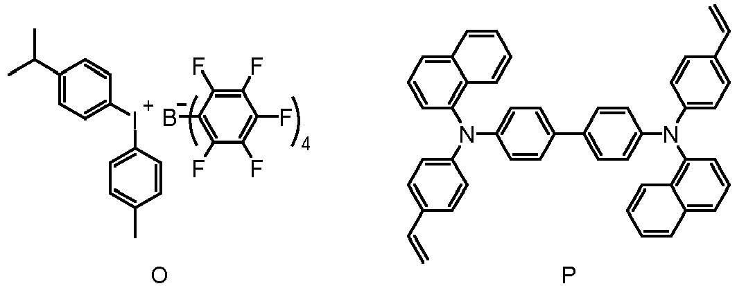

- In the above-mentioned process, the vapor deposition rate of the organic material was maintained at 0.4 to 0.7 Å/sec, the deposition rates of LiF and aluminum were maintained at 0.3 Å/sec and 2 Å/sec, respectively, and the degree of vacuum during the deposition was maintained at 2*10-7 to 5*10-8 torr.
- The organic light emitting devices were manufactured in the same manner as in Experimental Example 1, except that the compounds shown in Table 1 below were used instead of
Compound 1. - The organic light emitting devices were manufactured in the same manner as in Experimental Example 1, except that the compounds shown in Table 1 below were used instead of
Compound 1. - The driving voltage, external quantum efficiency (EQE), and lifetime were measured by applying a current of 10 mA/cm2 to the organic light emitting devices manufactured in the Experimental Examples and Comparative Experimental Examples, and the results are shown in Table 1 below. At this time, the external quantum efficiency (EQE) was calculated as "(the number of emitted photon)/(the number of injected charge carrier) * 100", and T90 means the time required for the luminance to be reduced to 90% of the initial luminance (500 nit).
[Table 1] Category Compound (Dopant of the light emitting layer) Driving voltage (V@10mA/cm2) EQE (%@10mA/cm2) Lifetime (hr) (T90@500 nit) Experimental Example 1 Compound 14.56 6.05 254 Experimental Example 2 Compound 24.58 6.08 260 Experimental Example 3 Compound 34.62 6.07 265 Experimental Example 4 Compound 44.63 6.06 249 Experimental Example 5 Compound 54.69 5.98 252 Experimental Example 6 Compound 64.70 6.10 260 Experimental Example 7 Compound 74.59 6.01 259 Experimental Example 8 Compound 84.62 5.99 260 Experimental Example 9 Compound 9 4.69 6.05 249 Experimental Example 10 Compound 10 4.68 6.03 258 Experimental Example 11 Compound 11 4.61 6.01 269 Experimental Example 12 Compound 12 4.62 6.05 287 Experimental Example 13 Compound 13 4.68 6.06 268 Experimental Example 14 Compound 14 4.69 5.99 257 Experimental Example 15 Compound 15 4.72 5.97 261 Experimental Example 16 Compound 16 4.75 6.03 258 Experimental Example 17 Compound 17 4.68 6.06 260 Experimental Example 18 Compound 18 4.65 6.08 258 Experimental Example 19 Compound 19 4.59 6.07 267 Experimental Example 20 Compound 20 4.63 6.09 255 Experimental Example 21 Compound 21 4.70 5.98 251 Experimental Example 22 Compound 22 4.68 6.05 260 Comparative Experimental Example 1 Compound F 4.69 4.39 105 Comparative Experimental Example 2 Compound G 4.68 4.23 99 Comparative Experimental Example 3 Compound H 4.62 3.98 83 - As shown in Table 1 above, the organic light emitting devices comprising the compounds of the present disclosure exhibits excellent characteristics in terms of efficiency, driving voltage and lifetime of the organic light emitting device.
-
1: substrate 2: anode 3: light emitting layer 4: cathode 5: hole injection layer 6: hole transport layer 7: light emitting layer 8: electron injection and transport layer
Claims (11)
- A compound represented by the following Chemical Formula 1:
 Ar1 is benzene fused with an adjacent ring, or benzothiophene,Ar2 is benzene fused with two adjacent rings,R1 and R2 are each independently hydrogen, deuterium, a substituted or unsubstituted C1-60 alkyl, or a substituted or unsubstituted C6-60 aryl, or two adjacent R1 or R2 are combined with each other to form a substituted or unsubstituted C3-10 cycloalkyl,R3 is a substituted or unsubstituted C1-60 alkyl, a substituted or unsubstituted C3-60 cycloalkyl, or a substituted or unsubstituted C6-60 aryl, or a substituent represented by any one of the following Chemical Formulas 2 to 4,
 each R4 is independently hydrogen, deuterium, or two adjacent R4s are combined with each other to form a substituted or unsubstituted C3-10 alkylene, or a substituted or unsubstituted C6-60 aromatic ring,
 R6 is independently hydrogen, deuterium, a substituted or unsubstituted C1-60 alkyl, or a substituted or unsubstituted C2-60 heteroaryl containing at least one heteroatom selected from the group consisting of N, O and S,n1 is an integer of 1 to 4,n2 is an integer of 0 to 5, andn3 and n4 are each independently an integer of 3 to 8.
 - The compound of claim 1 wherein:
the Chemical Formula 1 is represented by the following Chemical Formula 1-1 or Chemical Formula 1-2:

Ar2, R1, R2, R3, n1, n2, n3, and n4 are as defined in claim 1. - The compound of claim 1 wherein:
the Chemical Formula 1 is represented by any one selected from the group consisting of the following Chemical Formula 1-3 to Chemical Formula 1-5:


Ar1, Ar2, R1, R2, R3, n1, and n2 are as defined in claim 1. - The compound of claim 1 wherein:
R1 is hydrogen, deuterium, or tertbutyl, or two adjacent R1s are combined with each other to form a substituted or unsubstituted C5-10 cycloalkyl. - The compound of claim 1 wherein:
R1 is hydrogen, deuterium, or tertbutyl, or two adjacent R1s are combined with each other to form a substituent represented by any one of the following:
- The compound of claim 1 wherein:
R2 is hydrogen, deuterium, tertbutyl, phenyl, or phenyl substituted with tertbutyl, or two adjacent Rzs are combined with each other to form a substituted or unsubstituted C5-10 cycloalkyl. - The compound of claim 1 wherein:
R2 is hydrogen, deuterium, tertbutyl, phenyl, or phenyl substituted with tertbutyl, or two adjacent Rzs are combined with each other to form a substituent represented by any one of the following:
- The compound of claim 1 wherein:
R3 is methyl, isopropyl, tertbutyl, cyclohexyl, phenyl, adamantyl, or a substituent represented by any one of the following:


- The compound of claim 1 wherein:
the compound represented by Chemical Formula 1 is any one selected from the group consisting of the following compounds:


- An organic light emitting device comprising: a first electrode; a second electrode that is provided opposite to the first electrode; and one or more organic material layers that are provided between the first electrode and the second electrode, wherein one or more layers of the organic material layers comprises the compound as set forth in any one of claims 1 to 9.
- The organic light emitting device of claim 10, wherein:
the organic material layer is a light emitting layer.
Applications Claiming Priority (2)
| Application Number | Priority Date | Filing Date | Title |
|---|---|---|---|
| KR1020210122662A KR20230039393A (en) | 2021-09-14 | 2021-09-14 | Novel compound and organic light emitting device comprising the same |
| PCT/KR2022/011130 WO2023043044A1 (en) | 2021-09-14 | 2022-07-28 | Novel compound and organic light emitting device comprising same |
Publications (1)
| Publication Number | Publication Date |
|---|---|
| EP4335854A1 true EP4335854A1 (en) | 2024-03-13 |
Family
ID=85603082
Family Applications (1)
| Application Number | Title | Priority Date | Filing Date |
|---|---|---|---|
| EP22870131.4A Pending EP4335854A1 (en) | 2021-09-14 | 2022-07-28 | Novel compound and organic light emitting device comprising the same |
Country Status (4)
| Country | Link |
|---|---|
| EP (1) | EP4335854A1 (en) |
| KR (1) | KR20230039393A (en) |
| CN (1) | CN117480173A (en) |
| WO (1) | WO2023043044A1 (en) |
Family Cites Families (7)
| Publication number | Priority date | Publication date | Assignee | Title |
|---|---|---|---|---|
| KR100430549B1 (en) | 1999-01-27 | 2004-05-10 | 주식회사 엘지화학 | New organomattalic complex molecule for the fabrication of organic light emitting diodes |
| DE10135513B4 (en) | 2001-07-20 | 2005-02-24 | Novaled Gmbh | Light-emitting component with organic layers |
| US10686141B2 (en) * | 2016-09-07 | 2020-06-16 | Kwansei Gakuin Educational Foundation | Polycyclic aromatic compound |
| KR101876763B1 (en) * | 2017-05-22 | 2018-07-11 | 머티어리얼사이언스 주식회사 | Organic compound and organic electroluminescent device comprising the same |
| WO2020054676A1 (en) * | 2018-09-10 | 2020-03-19 | 学校法人関西学院 | Organic electroluminescent element |
| US20220278278A1 (en) * | 2019-07-25 | 2022-09-01 | Cynora Gmbh | Organic molecules for optoelectronic devices |
| KR102239440B1 (en) * | 2019-07-31 | 2021-04-13 | 주식회사 엘지화학 | Multicyclic compound and organic light emitting device comprising the same |
-
2021
- 2021-09-14 KR KR1020210122662A patent/KR20230039393A/en unknown
-
2022
- 2022-07-28 CN CN202280040513.8A patent/CN117480173A/en active Pending
- 2022-07-28 EP EP22870131.4A patent/EP4335854A1/en active Pending
- 2022-07-28 WO PCT/KR2022/011130 patent/WO2023043044A1/en active Application Filing
Also Published As
| Publication number | Publication date |
|---|---|
| CN117480173A (en) | 2024-01-30 |
| WO2023043044A1 (en) | 2023-03-23 |
| KR20230039393A (en) | 2023-03-21 |
Similar Documents
| Publication | Publication Date | Title |
|---|---|---|
| EP4230629A1 (en) | Novel compound and organic light-emitting device comprising same | |
| EP4230630A1 (en) | Novel compound and organic light emitting device comprising same | |
| EP4227312A1 (en) | Novel compound and organic light emitting device comprising same | |
| KR20230039394A (en) | Novel compound and organic light emitting device comprising the same | |
| EP4335854A1 (en) | Novel compound and organic light emitting device comprising the same | |
| EP4279493A1 (en) | Novel compound and organic light-emitting device comprising same | |
| EP4242214A1 (en) | Novel compound and organic light emitting device using same | |
| EP4245760A1 (en) | Novel compound and organic light-emitting device comprising same | |
| EP4273151A1 (en) | Novel compound and organic light emitting device using same | |
| EP4265625A1 (en) | Novel compound and organic light emitting device comprising same | |
| EP4293030A1 (en) | Novel compound and organic light-emitting device using same | |
| EP4332107A1 (en) | Novel compound and organic light-emitting device using same | |
| EP4279492A1 (en) | Novel compound and organic light emitting device comprising same | |
| EP4092033A1 (en) | Novel compound and organic light-emitting device using same | |
| EP3778582B1 (en) | Novel compound, coating composition comprising the same and organic light emitting device comprising the same | |
| KR102653484B1 (en) | Novel compound and organic light emitting device comprising the same | |
| EP4137472A1 (en) | Novel compound and organic light-emitting device using same | |
| KR20230108602A (en) | Novel compound and organic light emitting device comprising the same | |
| KR20230125557A (en) | Novel compound and organic light emitting device comprising the same | |
| KR20230108600A (en) | Novel compound and organic light emitting device comprising the same | |
| KR20230108601A (en) | Novel compound and organic light emitting device comprising the same | |
| KR20220098673A (en) | Novel compound and organic light emitting device comprising the same | |
| KR20220098687A (en) | Novel compound and organic light emitting device comprising the same | |
| KR20220013229A (en) | Novel compound and organic light emitting device comprising the same | |
| KR20230170596A (en) | Novel compound and organic light emitting device comprising the same |
Legal Events
| Date | Code | Title | Description |
|---|---|---|---|
| STAA | Information on the status of an ep patent application or granted ep patent |
Free format text: STATUS: THE INTERNATIONAL PUBLICATION HAS BEEN MADE |
|
| PUAI | Public reference made under article 153(3) epc to a published international application that has entered the european phase |
Free format text: ORIGINAL CODE: 0009012 |
|
| STAA | Information on the status of an ep patent application or granted ep patent |
Free format text: STATUS: REQUEST FOR EXAMINATION WAS MADE |
|
| 17P | Request for examination filed |
Effective date: 20231207 |
|
| AK | Designated contracting states |
Kind code of ref document: A1 Designated state(s): AL AT BE BG CH CY CZ DE DK EE ES FI FR GB GR HR HU IE IS IT LI LT LU LV MC MK MT NL NO PL PT RO RS SE SI SK SM TR |