EP4334636B1 - Leuchtdiodenfilament - Google Patents
Leuchtdiodenfilament Download PDFInfo
- Publication number
- EP4334636B1 EP4334636B1 EP22726107.0A EP22726107A EP4334636B1 EP 4334636 B1 EP4334636 B1 EP 4334636B1 EP 22726107 A EP22726107 A EP 22726107A EP 4334636 B1 EP4334636 B1 EP 4334636B1
- Authority
- EP
- European Patent Office
- Prior art keywords
- led filament
- light
- leds
- led
- blocking wall
- Prior art date
- Legal status (The legal status is an assumption and is not a legal conclusion. Google has not performed a legal analysis and makes no representation as to the accuracy of the status listed.)
- Active
Links
Images


Classifications
-
- F—MECHANICAL ENGINEERING; LIGHTING; HEATING; WEAPONS; BLASTING
- F21—LIGHTING
- F21K—NON-ELECTRIC LIGHT SOURCES USING LUMINESCENCE; LIGHT SOURCES USING ELECTROCHEMILUMINESCENCE; LIGHT SOURCES USING CHARGES OF COMBUSTIBLE MATERIAL; LIGHT SOURCES USING SEMICONDUCTOR DEVICES AS LIGHT-GENERATING ELEMENTS; LIGHT SOURCES NOT OTHERWISE PROVIDED FOR
- F21K9/00—Light sources using semiconductor devices as light-generating elements, e.g. using light-emitting diodes [LED] or lasers
- F21K9/20—Light sources comprising attachment means
- F21K9/23—Retrofit light sources for lighting devices with a single fitting for each light source, e.g. for substitution of incandescent lamps with bayonet or threaded fittings
- F21K9/232—Retrofit light sources for lighting devices with a single fitting for each light source, e.g. for substitution of incandescent lamps with bayonet or threaded fittings specially adapted for generating an essentially omnidirectional light distribution, e.g. with a glass bulb
-
- F—MECHANICAL ENGINEERING; LIGHTING; HEATING; WEAPONS; BLASTING
- F21—LIGHTING
- F21K—NON-ELECTRIC LIGHT SOURCES USING LUMINESCENCE; LIGHT SOURCES USING ELECTROCHEMILUMINESCENCE; LIGHT SOURCES USING CHARGES OF COMBUSTIBLE MATERIAL; LIGHT SOURCES USING SEMICONDUCTOR DEVICES AS LIGHT-GENERATING ELEMENTS; LIGHT SOURCES NOT OTHERWISE PROVIDED FOR
- F21K9/00—Light sources using semiconductor devices as light-generating elements, e.g. using light-emitting diodes [LED] or lasers
- F21K9/20—Light sources comprising attachment means
- F21K9/23—Retrofit light sources for lighting devices with a single fitting for each light source, e.g. for substitution of incandescent lamps with bayonet or threaded fittings
- F21K9/237—Details of housings or cases, i.e. the parts between the light-generating element and the bases; Arrangement of components within housings or cases
-
- F—MECHANICAL ENGINEERING; LIGHTING; HEATING; WEAPONS; BLASTING
- F21—LIGHTING
- F21K—NON-ELECTRIC LIGHT SOURCES USING LUMINESCENCE; LIGHT SOURCES USING ELECTROCHEMILUMINESCENCE; LIGHT SOURCES USING CHARGES OF COMBUSTIBLE MATERIAL; LIGHT SOURCES USING SEMICONDUCTOR DEVICES AS LIGHT-GENERATING ELEMENTS; LIGHT SOURCES NOT OTHERWISE PROVIDED FOR
- F21K9/00—Light sources using semiconductor devices as light-generating elements, e.g. using light-emitting diodes [LED] or lasers
- F21K9/60—Optical arrangements integrated in the light source, e.g. for improving the colour rendering index or the light extraction
- F21K9/68—Details of reflectors forming part of the light source
-
- F—MECHANICAL ENGINEERING; LIGHTING; HEATING; WEAPONS; BLASTING
- F21—LIGHTING
- F21K—NON-ELECTRIC LIGHT SOURCES USING LUMINESCENCE; LIGHT SOURCES USING ELECTROCHEMILUMINESCENCE; LIGHT SOURCES USING CHARGES OF COMBUSTIBLE MATERIAL; LIGHT SOURCES USING SEMICONDUCTOR DEVICES AS LIGHT-GENERATING ELEMENTS; LIGHT SOURCES NOT OTHERWISE PROVIDED FOR
- F21K9/00—Light sources using semiconductor devices as light-generating elements, e.g. using light-emitting diodes [LED] or lasers
- F21K9/90—Methods of manufacture
-
- F—MECHANICAL ENGINEERING; LIGHTING; HEATING; WEAPONS; BLASTING
- F21—LIGHTING
- F21Y—INDEXING SCHEME ASSOCIATED WITH SUBCLASSES F21K, F21L, F21S and F21V, RELATING TO THE FORM OR THE KIND OF THE LIGHT SOURCES OR OF THE COLOUR OF THE LIGHT EMITTED
- F21Y2103/00—Elongate light sources, e.g. fluorescent tubes
- F21Y2103/10—Elongate light sources, e.g. fluorescent tubes comprising a linear array of point-like light-generating elements
-
- F—MECHANICAL ENGINEERING; LIGHTING; HEATING; WEAPONS; BLASTING
- F21—LIGHTING
- F21Y—INDEXING SCHEME ASSOCIATED WITH SUBCLASSES F21K, F21L, F21S and F21V, RELATING TO THE FORM OR THE KIND OF THE LIGHT SOURCES OR OF THE COLOUR OF THE LIGHT EMITTED
- F21Y2105/00—Planar light sources
- F21Y2105/10—Planar light sources comprising a two-dimensional array of point-like light-generating elements
- F21Y2105/14—Planar light sources comprising a two-dimensional array of point-like light-generating elements characterised by the overall shape of the two-dimensional array
- F21Y2105/16—Planar light sources comprising a two-dimensional array of point-like light-generating elements characterised by the overall shape of the two-dimensional array square or rectangular, e.g. for light panels
-
- F—MECHANICAL ENGINEERING; LIGHTING; HEATING; WEAPONS; BLASTING
- F21—LIGHTING
- F21Y—INDEXING SCHEME ASSOCIATED WITH SUBCLASSES F21K, F21L, F21S and F21V, RELATING TO THE FORM OR THE KIND OF THE LIGHT SOURCES OR OF THE COLOUR OF THE LIGHT EMITTED
- F21Y2113/00—Combination of light sources
- F21Y2113/30—Combination of light sources of visible and non-visible spectrum
-
- F—MECHANICAL ENGINEERING; LIGHTING; HEATING; WEAPONS; BLASTING
- F21—LIGHTING
- F21Y—INDEXING SCHEME ASSOCIATED WITH SUBCLASSES F21K, F21L, F21S and F21V, RELATING TO THE FORM OR THE KIND OF THE LIGHT SOURCES OR OF THE COLOUR OF THE LIGHT EMITTED
- F21Y2115/00—Light-generating elements of semiconductor light sources
- F21Y2115/10—Light-emitting diodes [LED]
Definitions
- the present invention relates to an LED (light emitting diode) filament.
- the present invention also relates to an LED filament lamp comprising at least one such LED filament.
- the present invention also relates to a method of manufacturing an LED filament.
- Incandescent lamps are rapidly being replaced by LED (light emitting diode) based lighting solutions. It is nevertheless appreciated and desired by users to have retrofit lamps which have the look of an incandescent bulb. For this purpose, one can simply make use of the infrastructure for producing incandescent lamps based on glass and replace the filament with LEDs emitting white light.
- One of the concepts is based on LED filaments placed in such a bulb. The appearances of these lamps are highly appreciated as they look highly decorative.
- a regular tuneable white filament lamp consists of at least two LED filaments, one with low CCT (correlated color temperature) LEDs and one with high CCT LEDs, or a filament with a combination of low and high CCT LEDs.
- the color LEDs can be added into the lamp as a separate filament or can be placed on same surface of filament substrate together with the white LEDs.
- LED light sources are composed of mini-LED chips with the relatively small sizes, so that the number of the LED light sources capable of being contained in a lampshade is increased, the whole LED luminescent lamp can show more color types, and free showing and switching of multiple colors can be achieved.
- the present invention is based on the understanding that by arranging a light-blocking wall between the first and second LED filament portions of the filament, e.g. between a first string of white LEDs and a second string of RGB LEDs, unwanted intra-filament optical cross-talk may indeed be reduced or prevented. Accordingly, the present LED filament can have a not reduced color-gamut area and/or can achieve saturated color points.
- an LED filament is providing LED filament light and comprises a plurality of light emitting diodes (LEDs) arranged in a linear array.
- the LED filament has a length L and a width W, wherein L>5W.
- the LED filament may be arranged in a straight configuration or in a non-straight configuration such as for example a curved configuration, a 2D/3D spiral or a helix.
- the LEDs are arranged on an elongated carrier like for instance a substrate, that may be rigid (made from e.g. a polymer, glass, quartz, metal or sapphire) or flexible (e.g. made of a polymer or metal e.g. a film or foil).
- the LEDs are arranged on at least one of these surfaces.
- the carrier may be reflective or light transmissive, such as translucent and preferably transparent.
- the LED filament may comprise an encapsulant at least partly covering at least part of the plurality of LEDs.
- the encapsulant may also at least partly cover at least one of the first major or second major surface.
- the encapsulant may be a polymer material which may be flexible such as for example a silicone.
- the LEDs may be arranged for emitting LED light e.g. of different colors or spectrums.
- the encapsulant may comprise a luminescent material that is configured to at least partly convert LED light into converted light.
- the luminescent material may be a phosphor such as an inorganic phosphor and/or quantum dots or rods.
- the LED filament may comprise multiple sub-filaments.
- the plurality of first LEDs may be arranged on a surface of the first LED filament portion, wherein the plurality of second LEDs are arranged on a corresponding surface of the second LED filament portion such that the first LEDs are aimed in substantially the same direction(s) as the second LEDs, and wherein the at least one light-blocking wall raises above said surface of the first LED filament portion and the corresponding surface of the second LED filament portion.
- the at least one wall may block light just where it is needed.
- the at least one light-blocking wall may have a height that exceeds the height of the first and second LEDs including any encapsulation thereof. At least one light-blocking wall of this height may indeed prevent most or all optical cross-talk between the first and second LEDs.
- the first LED filament portion comprises a first elongated carrier
- the second LED filament portion comprises a second elongated carrier
- the first elongated carrier is mechanically connected to the second elongated carrier by at least one non-transparent layer.
- the at least one light-blocking wall is formed by the at least one non-transparent layer.
- said at least one non-transparent layer is bent along a boundary between the first LEDs and the second LEDs to form said at least one light-blocking wall.
- the at least one non-transparent layer may already be present in a PCB or FPC used to form the present LED filament portions, whereby the manufacturing process of this LED filament is simplified, since the need for any additional material deposition step for creation of a separation light-blocking wall may be eliminated.
- This is also a very thin way of preventing cross-talk, without compromising targeted aesthetics.
- the light-blocking wall(s) could be made out of any type of thin non-transparent bendable material, for example the aforementioned metallization layer, a local region of a flexible PCB covered with solder resist or paint, a region of a non-transparent flexible PCB, etc.
- the at least one non-transparent layer could be generally non-transparent for all light (red, green, blue, UV, white) or selectively non-transparent (e.g. blocking blue but transmitting red). Accordingly, the at least one light-blocking wall may generally block (all) light or just block some type of light (e.g. blue).
- the at least one non-transparent layer may be bent such that the at least one light-blocking wall is at least one fin-type light-blocking wall.
- the at least one non-transparent layer could alternatively be bent to include a rectangular fin, for example.
- the at least one light-blocking wall may be adapted to block LED filament light of a first color but not block LED filament light of at least a second color different than the first color.
- the at least one light-blocking wall may be adapted to block blue LED filament light but not block (i.e. transmit) LED filament light of other colors.
- the at least one light-blocking wall may be segmented into wall segments along the length of the LED filament, wherein the wall segments are situated at the locations of the first and second LEDs along the LED filament, and wherein gaps with reduced or no wall height are situated at locations along the LED filament where no first or second LEDs are present.
- Such segmental structure of the light-blocking wall will allow bending of the LED filament along the length of the filament for required level of flexibility.
- the wall segments (or 'fins') at the first and second LEDs will allow to decrease locally a stress to LED chips solder points by limiting locally a radius of bending curvature for a flexible LED filament.
- the LED filament may be segmentally bent along the length of the LED filament by bending (only) at said gaps.
- the wall segments are also located at the position of first and second LEDs to block the light most efficiently.
- Each wall segment may have an isosceles trapezoid side view profile with a wider base than top.
- the LED filament may be subject to not only convex bending, but also (some) concave bending without adjoining wall segments interfering with each other.
- the first LEDs may be white LEDs for emitting white first LED filament light
- the second LEDs are RGB (red green blue) LEDs for emitting colored second LED filament light
- the white LEDs may be blue and/or UV LED chips encapsulated by an encapsulant comprising a luminescent material adapted to at least partly convert blue and/or UV LED light into converted LED light. Accordingly, the at least one light-blocking wall may prevent light emitted by direct blue LEDs of the RGB LEDs from being absorbed by the encapsulant/luminescent material encapsulating the blue/UV LED chips of the white LEDs, which otherwise would have caused unwanted phosphorescence and unwanted red-yellow light generation.
- the LED filament may further comprise: a third LED filament portion parallel to the second LED filament portion and comprising a plurality of third LEDs adapted to emit third LED filament light; and at least one further light-blocking wall arranged between the second LED filament portion and the third LED filament portion to prevent optical cross-talk between the second and third LEDs.
- the at least one further light-blocking wall could have the same features as the previously mentioned light-blocking wall.
- the third LEDs may be white LEDs for emitting white third LED filament light of a different color temperature than the white first LED filament light. This gives the possibility to create different color temperatures as well as colored light using the same LED filament (without crosstalk).
- the color temperature CT1 of the white first LED filament light could be ⁇ 2500K, e.g. 2200K.
- the color temperature CT2 of the white third LED filament light could be >2700K, e.g. 3500K.
- the difference between CT2 and CT1 could be greater than 500K (CT2-CT1>500K).
- the three LED filament portions are used provide: warm white WW + RGB for colors + cool white CW.
- the order could be warm white WW + cool white CW (no RGB for colors) or warm white WW + cool white CW + RGB for colors or cool white CW + warm white WW + RGB for colors.
- whites of 2 CCT types may be separated from each other, and any white CCT string may be separated from individual R, G, and B chips or RGB clusters.
- the LED filament could further comprise a fourth parallel LED filament portion, or a fourth parallel LED filament portion and a fifth parallel LED filament portion.
- an LED filament lamp comprising: at least one LED filament according to the first aspect; a light transmissive (translucent, preferably transparent) envelope at least partly surrounding said at least one LED filament arrangement; and a connector for electrically and mechanically connecting the LED filament lamp to a socket.
- the LED filament lamp may for example be retrofit light bulb.
- the LED filament lamp could further comprise a controller for individually controlling the LED filament portions of the LED filament(s).
- the LED filament lamp could be color and/or color temperature tuneable.
- a method of manufacturing an LED filament comprising: providing a first LED filament portion comprising a first elongated carrier and a plurality of first LEDs adapted to emit first LED filament light; providing a second LED filament portion parallel to the first LED filament portion and comprising a second elongated carrier and a plurality of second LEDs adapted to emit second LED filament light, wherein the first elongated carrier is mechanically connected to the second elongated carrier by at least one substantially flat layer with excessive distance between the first and second elongated carriers; and bending the at least one substantially flat layer to form at least one light-blocking wall between the first LED filament portion and the second LED filament portion, whereby said excessive distance is reduced to a selected distance between the first and second elongated carriers.
- the at least one substantially flat layer may be segmented into bow tie shaped segments.
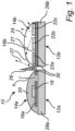
- Fig. 1 shows an LED filament 10 according to an embodiment of the present invention.
- the LED filament 10 is generally adapted to provide LED filament light.
- the LED filament 10 can for example have a straight configuration ( Fig. 7 ) or a bend configuration ( Fig. 3 ).
- the LED filament 10 comprises a first LED filament portion 12a.
- the first LED filament portion 12a comprises a plurality of first LEDs 14a adapted to emit first LED filament light.
- the first LEDs 14a may be arranged in a linear array along the length of the LED filament 10/first LED filament portion 12a.
- the first LEDs 14a may be arranged on a (first major) surface 16a of the first LED filament portion 12a.
- the first LEDs 14a may be white LEDs for emitting white first LED filament light.
- the white LEDs may be blue and/or UV LED chips 18 encapsulated by a first encapsulant 20 comprising a luminescent material adapted to at least partly convert blue and/or UV LED light into converted LED light.
- the LED filament 10 further comprises a second LED filament portion 12b.
- the second LED filament portion 12b is substantially parallel to the first LED filament portion 12a.
- the first and second LED filament portions 12a-b could also be referred to as a first and second sub-filaments 12a-b.
- the second LED filament portion 12b comprises a plurality of second LEDs 14b adapted to second LED filament light.
- the first LED filament light and the second LED filament light may form the aforementioned LED filament light.
- the second LEDs 14b may be arranged in a linear array along the length of the LED filament 10 of the second LED filament portion 12b.
- the second LEDs 14b may be arranged on a corresponding (first major) surface 16b of the second LED filament portion 12b, such that the second LEDs 14b are aimed in substantially the same direction(s) as the first LEDs 14a.
- the second LEDs 14b may be RGB (red green blue) LEDs 22a-c for emitting colored second LED filament light.
- the RGB LEDs 22a-c may be encapsulated by a second encapsulant 24.
- the second encapsulant 24 may comprise a light scattering material.
- the LED filament 10 further comprises at least one light-blocking wall 26.
- the at least one light-blocking wall 26 is arranged between the first and second LED filament portions 12a-b.
- the at least one light-blocking wall 26 serves to prevent or at least reduce optical cross-talk between the first and second LEDs 14a-b.
- the at least one light-blocking wall 26 prevents light 27 emitted by direct blue LEDs 22c of the RGB LEDs from being absorbed by the first encapsulant 20, luminescent material encapsulating the blue/UV LED chips 18, which otherwise would have caused unwanted phosphorescence and unwanted red-yellow light generation.
- the present LED filament 10 can have a not reduced color-gamut area and/or can achieve saturated color points.
- the at least one light-blocking wall 26 raises above the surfaces 16a-b on which the first and second LEDs 14a-b are arranged.
- the at least one light-blocking wall 26 has a height h that exceeds the height of the first and second LEDs 14a-b including the encapsulations 20, 24.
- the height h of the at least one light-blocking wall 26 may for example be in the range of 0.1-3 mm or preferably in the range of 0.1-2 mm.
- the at least one light-blocking wall 26 may extend along (substantially) the complete length of the LED filament 10 or along only a portion or portions of the length of the LED filament 10.
- the elongated carrier 28a of the first LED filament portion 12a is mechanically connected to the elongated carrier 28b of the second LED filament portion 12b by at least one non-transparent layer 30.
- the at least one light-blocking wall 26 is formed by (some of) the at least one non-transparent layer 30.
- the at least one non-transparent layer 30 may be bent along a boundary 31 between the first and second LEDs 14a-b to form the at least one light-blocking wall 26.
- the at least one non-transparent layer 30 may for example be bent such that the at least one light-blocking wall 26 is at least one fin-type light-blocking wall with a ⁇ -shaped cross section, as seen in Fig. 1 .
- the at least one non-transparent layer 30 may for example be metallization/metallized layers between different lines of the LED filament 10.
- the at least one non-transparent layer 30 may be a blue filter blocking just the blue light 27. That is, the at least one light-blocking wall 26 may be adapted to block LED filament light of a first color (blue) but not block (but instead transmit) LED filament light of at least a second color different than the first color.
- the at least one light-blocking wall 26 may be segmented into wall segments 32a-c along the length of the LED filament 10. There can be one wall segment per first/second LED.
- the wall segments 32a-c are preferably situated at the locations of the first and second LEDs 14a-b along the LED filament 10, whereas gaps 34a-b with reduced or no wall height are situated at locations along the LED filament 10 where no first or second LEDs 14a-b are present.
- Such a segmental structure allows the LED filament 10 to be segmentally bent ( Fig. 3 ).
- Each wall segments 32a-c may have an isosceles trapezoid side view profile, with a wider base 36 than top 38.
- the LED filament 10 may be subject to not only convex bending ( Fig. 3 ), but also concave bending (not shown).
- the elongated carriers 28a-b may here be flexible to allow the bending of the LED filament 10 as in Fig. 3 .
- the LED filament 10 could also be (segmentally) twisted, to a spiral configuration, i.e. like a coil. In that case, the elongated carriers 28a-b could have appropriate notches (not shown) to allow the twisting.
- the LED filament 10 may be manufactured as follows.
- the first LED filament portion 12a comprising the first elongated carrier 28a and the plurality of first LEDs 14a is provided.
- the second LED filament portion 12b comprising the second elongated carrier 28b and the plurality of second LEDs 14b is provided.
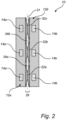
- the first elongated carrier 28a is mechanically connected to the second elongated carrier 28b by at least one substantially flat layer 30 with an excessive distance D between the first and second elongated carriers 28a-b, see Fig. 5a .
- the at least one substantially flat layer 30 may be the aforementioned non-transparent layer(s) 30.
- the at least one substantially flat layer 30 may be segmented into bow tie shaped segments as shown in Fig. 5a . It is appreciated that S1 and S2 could be performed at substantially the same time and/or combined.
- the at least one substantially flat layer 30 is bent to form the at least one light-blocking wall 26 between the first and second LED filament portions 12a-b.
- the at least one substantially flat layer 30 may be bent at three fold lines 40a-c, to form the at least one light-blocking wall 26 with ⁇ -shaped cross section.
- the excessive distance is consequently reduced to a selected (short) distance d between the first and second elongated carriers 28a-b, see Fig. 5b .
- Fig. 6 shows an LED filament 10 according to another embodiment of the present invention.
- the LED filament 10 in Fig. 6 may be similar to the previously discussed and shown LED filament, but further comprises a third LED filament portion (or sub-filament) 12c.
- the third LED filament portion 12c is substantially parallel to the second LED filament portion 12b.
- the third LED filament portion 12c may be arranged on the opposite side of the second LED filament portion 12b compared to the first LED filament portion 12a. In other words, the second LED filament portion 12b may be arranged between the first and third LED filament portions 12a and 12c.
- the third LED filament portion 12c comprises a plurality of third LEDs 14c adapted to emit third LED filament light.
- the third LEDs 14c may be arranged in a linear array along the length of the LED filament 10/third LED filament portion 12c.
- the third LEDs 14c may be white LEDs for emitting white third LED filament light.
- These white LEDs 14c may be blue and/or UV LED chips 18 encapsulated by a third encapsulant 42 comprising a luminescent material adapted to at least partly convert blue and/or UV LED light into converted LED light.
- the white third LED filament light can have a different color temperature than the white first LED filament light.
- the color temperature CT1 of the white first LED filament light could be ⁇ 2500K, whereas the color temperature CT2 of the white third LED filament light could be >2700K.
- the LED filament 10 in Fig. 6 also comprises at least one further light-blocking wall 26' arranged between the second LED filament portion 12b and the third LED filament portion 12c.
- the at least one further light-blocking wall 26' serves to prevent or at least reduce optical cross-talk between the second and third LEDs 14b-c.
- the at least one further light-blocking wall 26' prevents light 27 emitted by direct blue LEDs 22c of the RGB LEDs from being absorbed by the third encapsulant 42/luminescent material encapsulating the blue/UV LED chips 18 of the third LEDs 14c.
- the at least one further light-blocking wall 26' could have the one or more of the same features as the previously mentioned light-blocking wall 26.
- Fig. 7 shows an LED filament lamp 100, namely a retrofit light bulb.
- the lamp 100 comprises at least one LED filament 10 according to one or more embodiments of the present invention.
- the LED filament 10 in Fig. 7 has a straight (non-bent) configuration.
- the LED filament 10 in Fig. 7 has a (substantially) vertical orientation.
- the lamp 100 further comprises a transparent envelop 102 surrounding the LED filament 10.
- the envelop 102 can be clear.
- the envelop 102 is preferably made of glass.
- the envelop 102 may have various shapes.
- the lamp 100 further comprises a threaded connector/cap 104 for electrically and mechanically connecting for the lamp 100 to an external socket (not shown).
- the connector/cap 106 can be of various types known per se, for example E14 or E27.
- the lamp 100 may further comprise a controller (not shown) for individually controlling the LED filament portions/sub-filaments of the LED filament 10.
Landscapes
- Engineering & Computer Science (AREA)
- Physics & Mathematics (AREA)
- Microelectronics & Electronic Packaging (AREA)
- Optics & Photonics (AREA)
- General Engineering & Computer Science (AREA)
- Manufacturing & Machinery (AREA)
- Non-Portable Lighting Devices Or Systems Thereof (AREA)
Claims (14)
- LED-Filament (10) umfassend:einen ersten LED-Filamentabschnitt (12a), umfassend eine Vielzahl von ersten LEDs (14a), die angepasst sind, um erstes LED-Filamentlicht auszustrahlen;einen zweiten LED-Filamentabschnitt (12b) parallel zu dem ersten LED-Filamentabschnitt (12a) und umfassend eine Vielzahl von zweiten LEDs (14b), die angepasst sind, um zweites LED-Filamentlicht auszustrahlen; undmindestens eine lichtblockierende Wand (26), die zwischen dem ersten LED-Filamentabschnitt und dem zweiten LED-Filamentabschnitt angeordnet ist, um optisches Übersprechen zwischen den ersten LEDs des ersten LED-Filamentabschnitts und den zweiten LEDs des zweiten LED-Filamentabschnitts zu verringern oder zu verhindern,wobei der erste LED-Filamentabschnitt einen ersten länglichen Träger (28a) umfasst, wobei der zweite LED-Filamentabschnitt einen zweiten länglichen Träger (28b) umfasst, wobei der erste längliche Träger durch mindestens eine nicht transparente Schicht (30) mit dem zweiten länglichen Träger mechanisch verbunden ist und wobei die mindestens eine lichtblockierende Wand (26) durch die mindestens eine nicht transparente Schicht (30) ausgebildet wird.
- LED-Filament nach Anspruch 1, wobei die Vielzahl von ersten LEDs auf einer Oberfläche (16a) des ersten LED-Filamentabschnitts angeordnet ist, wobei die Vielzahl von zweiten LEDs auf einer entsprechenden Oberfläche (16b) des zweiten LED-Filamentabschnitts derart angeordnet ist, dass die ersten LEDs im Wesentlichen in die gleiche(n) Richtung(en) wie die zweiten LEDs gerichtet sind, und wobei sich die mindestens eine lichtblockierende Wand über die Oberfläche (16a) des ersten LED-Filamentabschnitts und die entsprechende Oberfläche (16b) des zweiten LED-Filamentabschnitts erhebt.
- LED-Filament nach Anspruch 1 oder 2, wobei die mindestens eine lichtblockierende Wand eine Höhe (h) aufweist, die die Höhe der ersten und der zweiten LEDs einschließlich jeweiliger Einkapselung davon übersteigt.
- LED-Filament nach einem der vorstehenden Ansprüche, wobei die mindestens eine nicht transparente Schicht entlang einer Grenze zwischen den ersten LEDs und den zweiten LEDs gebogen ist, um die mindestens eine lichtblockierende Wand auszubilden.
- LED-Filament nach einem der vorstehenden Ansprüche, wobei die mindestens eine nicht transparente Schicht derart gebogen ist, dass die mindestens eine lichtblockierende Wand mindestens eine lichtblockierende Wand von einem Lamellentyp ist.
- LED-Filament nach einem der vorstehenden Ansprüche, wobei die mindestens eine lichtblockierende Wand angepasst ist, um LED-Filamentlicht einer ersten Farbe zu blockieren, jedoch kein LED-Filamentlicht von mindestens einer zweiten Farbe zu blockieren, die sich von der ersten Farbe unterscheidet.
- LED-Filament nach einem der vorstehenden Ansprüche, wobei die mindestens eine lichtblockierende Wand entlang der Länge des LED-Filaments in Wandsegmente (32a-c) segmentiert ist, wobei die Wandsegmente an den Stellen der ersten und der zweiten LEDs entlang des LED-Filaments platziert sind, und wobei Lücken (34a-b) mit verringerter oder keiner Wandhöhe an Stellen entlang des LED-Filaments platziert sind, an denen keine ersten oder zweiten LEDs vorhanden sind.
- LED-Filament nach Anspruch 7, das entlang der Länge des LED-Filaments durch Biegen an den Lücken segmentweise gebogen ist.
- LED-Filament nach Anspruch 7 oder 8, wobei jedes Wandsegment ein gleichschenkliges trapezförmiges Seitenansichtsprofil mit einer breiteren Basis (36) als eine Oberseite (38) aufweist.
- LED-Filament nach einem der vorstehenden Ansprüche, wobei die ersten LEDs weiße LEDs zum Ausstrahlen von weißem ersten LED-Filamentlicht sind und wobei die zweiten LEDs RGB-LEDs zum Ausstrahlen von farbigem zweiten LED-Filamentlicht sind.
- LED-Filament nach einem der vorstehenden Ansprüche, ferner umfassend:einen dritten LED-Filamentabschnitt (12c) parallel zu dem zweiten LED-Filamentabschnitt und umfassend eine Vielzahl von dritten LEDs (14c), die angepasst sind, um drittes LED-Filamentlicht auszustrahlen; undmindestens eine weitere lichtblockierende Wand (26'), die zwischen dem zweiten LED-Filamentabschnitt und dem dritten LED-Filamentabschnitt angeordnet ist, um optisches Übersprechen zwischen den zweiten und den dritten LEDs zu verringern oder zu verhindern.
- LED-Filament nach den Ansprüchen 10 und 11, wobei die dritten LEDs weiße LEDs zum Ausstrahlen von weißem dritten LED-Filamentlicht mit einer unterschiedlichen Farbtemperatur als das weiße erste LED-Filamentlicht sind.
- LED-Filamentlampe (100), umfassend:mindestens ein LED-Filament (10) nach einem der vorstehenden Ansprüche;eine lichtdurchlässige Hülle (102), die die mindestens LED-Filamentanordnung mindestens teilweise umhüllt; undeinen Stecker (104) zum elektrischen und mechanischen Verbinden der LED-Filamentlampe mit einer Fassung.
- Verfahren zum Herstellen eines LED-Filaments (100), wobei das Verfahren umfasst:Bereitstellen eines ersten LED-Filamentabschnitts (12a), umfassend einen ersten länglichen Träger (28a) und eine Vielzahl von ersten LEDs (14a), die angepasst sind, um erstes LED-LED-Filamentlicht auszustrahlen;Bereitstellen eines zweiten LED-Filamentabschnitts (12b) parallel zu dem ersten LED-Filamentabschnitt und umfassend einen zweiten länglichen Träger (28b) und eine Vielzahl von zweiten LEDs (14b), die angepasst sind, um zweites LED-Filamentlicht auszustrahlen, wobei der erste längliche Träger mit dem zweiten länglichen Träger durch mindestens eine im Wesentlichen flache Schicht (30) mit übermäßigem Abstand (D) zwischen dem ersten und dem zweiten länglichen Träger mechanisch verbunden ist; undBiegen der mindestens einen im Wesentlichen flachen Schicht, um mindestens eine lichtblockierende Wand (26) zwischen dem ersten LED-Filamentabschnitt und dem zweiten LED-Filamentabschnitt auszubilden, wodurch der übermäßige Abstand auf einen ausgewählten Abstand (d) zwischen dem ersten und dem zweiten länglichen Träger verringert wird.
Applications Claiming Priority (2)
| Application Number | Priority Date | Filing Date | Title |
|---|---|---|---|
| EP21172834 | 2021-05-07 | ||
| PCT/EP2022/061399 WO2022233715A1 (en) | 2021-05-07 | 2022-04-28 | Light emitting diode filament |
Publications (3)
| Publication Number | Publication Date |
|---|---|
| EP4334636A1 EP4334636A1 (de) | 2024-03-13 |
| EP4334636C0 EP4334636C0 (de) | 2024-12-11 |
| EP4334636B1 true EP4334636B1 (de) | 2024-12-11 |
Family
ID=75936679
Family Applications (1)
| Application Number | Title | Priority Date | Filing Date |
|---|---|---|---|
| EP22726107.0A Active EP4334636B1 (de) | 2021-05-07 | 2022-04-28 | Leuchtdiodenfilament |
Country Status (7)
| Country | Link |
|---|---|
| US (1) | US12222074B2 (de) |
| EP (1) | EP4334636B1 (de) |
| JP (1) | JP7575856B2 (de) |
| CN (1) | CN117280153A (de) |
| ES (1) | ES2999672T3 (de) |
| PL (1) | PL4334636T3 (de) |
| WO (1) | WO2022233715A1 (de) |
Families Citing this family (2)
| Publication number | Priority date | Publication date | Assignee | Title |
|---|---|---|---|---|
| CN120693482A (zh) * | 2023-02-16 | 2025-09-23 | 昕诺飞控股有限公司 | Led灯丝装置 |
| WO2025201945A1 (en) * | 2024-03-25 | 2025-10-02 | Signify Holding B.V. | A led filament |
Family Cites Families (15)
| Publication number | Priority date | Publication date | Assignee | Title |
|---|---|---|---|---|
| JP2010040720A (ja) | 2008-08-04 | 2010-02-18 | Sharp Corp | フレキシブルプリント配線板、電子機器モジュールおよび電子情報機器 |
| DE102011000657A1 (de) | 2011-02-11 | 2012-08-16 | Andree Jahnel | Beleuchtungsleiste |
| US10128426B1 (en) | 2013-11-11 | 2018-11-13 | Andrey Zykin | LS core LED connector system and manufacturing method |
| JP2016021555A (ja) | 2014-05-27 | 2016-02-04 | キヤノン・コンポーネンツ株式会社 | フレキシブルプリント配線板およびフレキシブル回路板 |
| CN204187337U (zh) | 2014-11-04 | 2015-03-04 | 浙江锐迪生光电有限公司 | 一种具有螺旋型led灯丝的led灯丝灯 |
| DE102015206808A1 (de) * | 2015-04-15 | 2016-10-20 | Osram Gmbh | Leuchtmittel mit LEDs |
| DE102015206805B4 (de) * | 2015-04-15 | 2022-10-27 | Ledvance Gmbh | Leuchtmittel mit LEDs |
| CN205655147U (zh) | 2016-03-30 | 2016-10-19 | 深圳佳比泰智能照明股份有限公司 | 一种全彩灯带及其系统 |
| KR20190007830A (ko) | 2017-07-14 | 2019-01-23 | 삼성전자주식회사 | 필라멘트형 led 광원 및 led 램프 |
| JP7399849B2 (ja) | 2017-09-15 | 2023-12-18 | ルミレッズ ホールディング ベーフェー | フレキシブルなライトストリップ |
| HUE063704T2 (hu) | 2019-01-21 | 2024-01-28 | Signify Holding Bv | Hangolható színû izzólámpa |
| WO2020173895A1 (en) | 2019-02-28 | 2020-09-03 | Signify Holding B.V. | Lighting device |
| PL3987218T3 (pl) | 2019-06-24 | 2023-05-02 | Signify Holding B.V. | Urządzenie oświetleniowe z możliwością sterowania temperaturą barwową zawierające różne włókna diod led |
| JP7649783B2 (ja) | 2019-11-15 | 2025-03-21 | シグニファイ ホールディング ビー ヴィ | Ledフィラメント及びledフィラメントランプ |
| CN112097129A (zh) | 2020-08-31 | 2020-12-18 | 杭州杭科光电集团股份有限公司 | 颜色可控的led发光灯 |
-
2022
- 2022-04-28 EP EP22726107.0A patent/EP4334636B1/de active Active
- 2022-04-28 US US18/559,085 patent/US12222074B2/en active Active
- 2022-04-28 JP JP2023568404A patent/JP7575856B2/ja active Active
- 2022-04-28 PL PL22726107.0T patent/PL4334636T3/pl unknown
- 2022-04-28 ES ES22726107T patent/ES2999672T3/es active Active
- 2022-04-28 WO PCT/EP2022/061399 patent/WO2022233715A1/en not_active Ceased
- 2022-04-28 CN CN202280033275.8A patent/CN117280153A/zh active Pending
Also Published As
| Publication number | Publication date |
|---|---|
| EP4334636A1 (de) | 2024-03-13 |
| PL4334636T3 (pl) | 2025-04-07 |
| CN117280153A (zh) | 2023-12-22 |
| JP7575856B2 (ja) | 2024-10-30 |
| JP2024516312A (ja) | 2024-04-12 |
| WO2022233715A1 (en) | 2022-11-10 |
| EP4334636C0 (de) | 2024-12-11 |
| US12222074B2 (en) | 2025-02-11 |
| ES2999672T3 (en) | 2025-02-26 |
| US20240230037A1 (en) | 2024-07-11 |
Similar Documents
| Publication | Publication Date | Title |
|---|---|---|
| JP7503132B2 (ja) | 発光デバイス | |
| EP4276353B1 (de) | Leuchtdiodenfilamentanordnung mit mindestens einer biegeeinheit | |
| CN114651532A (zh) | Led灯丝灯和制造螺旋led灯丝的方法 | |
| EP4334636B1 (de) | Leuchtdiodenfilament | |
| US11913608B2 (en) | LED filament arrangement | |
| CN114641646A (zh) | 包括三个类型的led的发光二极管灯丝 | |
| JP7362948B2 (ja) | Ledフィラメント及びランプ | |
| US20230092931A1 (en) | Omnidirectional light-emitting light bulb shell and light bulb having the same | |
| JP7096447B2 (ja) | 発光フィラメントを有する照明デバイス | |
| US20250204130A1 (en) | Light emitting diode filament having reduced optical cross-talk | |
| WO2020229462A1 (en) | Led filament arrangement | |
| EP4430337B1 (de) | Led-filament | |
| US20240209994A1 (en) | Led filament arrangement | |
| US12188622B2 (en) | Lighting device | |
| US20250189087A1 (en) | Led filament | |
| EP4659287A1 (de) | Led-filament | |
| WO2024153507A1 (en) | Led filament | |
| WO2025157711A1 (en) | A led filament arrangement | |
| WO2024188830A1 (en) | A led filament lamp |
Legal Events
| Date | Code | Title | Description |
|---|---|---|---|
| STAA | Information on the status of an ep patent application or granted ep patent |
Free format text: STATUS: UNKNOWN |
|
| STAA | Information on the status of an ep patent application or granted ep patent |
Free format text: STATUS: THE INTERNATIONAL PUBLICATION HAS BEEN MADE |
|
| PUAI | Public reference made under article 153(3) epc to a published international application that has entered the european phase |
Free format text: ORIGINAL CODE: 0009012 |
|
| STAA | Information on the status of an ep patent application or granted ep patent |
Free format text: STATUS: REQUEST FOR EXAMINATION WAS MADE |
|
| 17P | Request for examination filed |
Effective date: 20231207 |
|
| AK | Designated contracting states |
Kind code of ref document: A1 Designated state(s): AL AT BE BG CH CY CZ DE DK EE ES FI FR GB GR HR HU IE IS IT LI LT LU LV MC MK MT NL NO PL PT RO RS SE SI SK SM TR |
|
| GRAJ | Information related to disapproval of communication of intention to grant by the applicant or resumption of examination proceedings by the epo deleted |
Free format text: ORIGINAL CODE: EPIDOSDIGR1 |
|
| STAA | Information on the status of an ep patent application or granted ep patent |
Free format text: STATUS: GRANT OF PATENT IS INTENDED |
|
| GRAP | Despatch of communication of intention to grant a patent |
Free format text: ORIGINAL CODE: EPIDOSNIGR1 |
|
| DAV | Request for validation of the european patent (deleted) | ||
| DAX | Request for extension of the european patent (deleted) | ||
| INTG | Intention to grant announced |
Effective date: 20240703 |
|
| GRAS | Grant fee paid |
Free format text: ORIGINAL CODE: EPIDOSNIGR3 |
|
| GRAA | (expected) grant |
Free format text: ORIGINAL CODE: 0009210 |
|
| STAA | Information on the status of an ep patent application or granted ep patent |
Free format text: STATUS: THE PATENT HAS BEEN GRANTED |
|
| AK | Designated contracting states |
Kind code of ref document: B1 Designated state(s): AL AT BE BG CH CY CZ DE DK EE ES FI FR GB GR HR HU IE IS IT LI LT LU LV MC MK MT NL NO PL PT RO RS SE SI SK SM TR |
|
| REG | Reference to a national code |
Ref country code: GB Ref legal event code: FG4D |
|
| REG | Reference to a national code |
Ref country code: CH Ref legal event code: EP |
|
| REG | Reference to a national code |
Ref country code: DE Ref legal event code: R096 Ref document number: 602022008653 Country of ref document: DE |
|
| REG | Reference to a national code |
Ref country code: IE Ref legal event code: FG4D |
|
| U01 | Request for unitary effect filed |
Effective date: 20250106 |
|
| U07 | Unitary effect registered |
Designated state(s): AT BE BG DE DK EE FI FR IT LT LU LV MT NL PT RO SE SI Effective date: 20250115 |
|
| REG | Reference to a national code |
Ref country code: ES Ref legal event code: FG2A Ref document number: 2999672 Country of ref document: ES Kind code of ref document: T3 Effective date: 20250226 |
|
| PG25 | Lapsed in a contracting state [announced via postgrant information from national office to epo] |
Ref country code: HR Free format text: LAPSE BECAUSE OF FAILURE TO SUBMIT A TRANSLATION OF THE DESCRIPTION OR TO PAY THE FEE WITHIN THE PRESCRIBED TIME-LIMIT Effective date: 20241211 |
|
| PG25 | Lapsed in a contracting state [announced via postgrant information from national office to epo] |
Ref country code: NO Free format text: LAPSE BECAUSE OF FAILURE TO SUBMIT A TRANSLATION OF THE DESCRIPTION OR TO PAY THE FEE WITHIN THE PRESCRIBED TIME-LIMIT Effective date: 20250311 |
|
| PG25 | Lapsed in a contracting state [announced via postgrant information from national office to epo] |
Ref country code: GR Free format text: LAPSE BECAUSE OF FAILURE TO SUBMIT A TRANSLATION OF THE DESCRIPTION OR TO PAY THE FEE WITHIN THE PRESCRIBED TIME-LIMIT Effective date: 20250312 |
|
| PG25 | Lapsed in a contracting state [announced via postgrant information from national office to epo] |
Ref country code: RS Free format text: LAPSE BECAUSE OF FAILURE TO SUBMIT A TRANSLATION OF THE DESCRIPTION OR TO PAY THE FEE WITHIN THE PRESCRIBED TIME-LIMIT Effective date: 20250311 |
|
| U20 | Renewal fee for the european patent with unitary effect paid |
Year of fee payment: 4 Effective date: 20250424 |
|
| PG25 | Lapsed in a contracting state [announced via postgrant information from national office to epo] |
Ref country code: SM Free format text: LAPSE BECAUSE OF FAILURE TO SUBMIT A TRANSLATION OF THE DESCRIPTION OR TO PAY THE FEE WITHIN THE PRESCRIBED TIME-LIMIT Effective date: 20241211 |
|
| PGFP | Annual fee paid to national office [announced via postgrant information from national office to epo] |
Ref country code: PL Payment date: 20250422 Year of fee payment: 4 |
|
| PGFP | Annual fee paid to national office [announced via postgrant information from national office to epo] |
Ref country code: ES Payment date: 20250513 Year of fee payment: 4 |
|
| PG25 | Lapsed in a contracting state [announced via postgrant information from national office to epo] |
Ref country code: IS Free format text: LAPSE BECAUSE OF FAILURE TO SUBMIT A TRANSLATION OF THE DESCRIPTION OR TO PAY THE FEE WITHIN THE PRESCRIBED TIME-LIMIT Effective date: 20250411 |
|
| PG25 | Lapsed in a contracting state [announced via postgrant information from national office to epo] |
Ref country code: SK Free format text: LAPSE BECAUSE OF FAILURE TO SUBMIT A TRANSLATION OF THE DESCRIPTION OR TO PAY THE FEE WITHIN THE PRESCRIBED TIME-LIMIT Effective date: 20241211 |
|
| PGFP | Annual fee paid to national office [announced via postgrant information from national office to epo] |
Ref country code: TR Payment date: 20250415 Year of fee payment: 4 |
|
| PG25 | Lapsed in a contracting state [announced via postgrant information from national office to epo] |
Ref country code: CZ Free format text: LAPSE BECAUSE OF FAILURE TO SUBMIT A TRANSLATION OF THE DESCRIPTION OR TO PAY THE FEE WITHIN THE PRESCRIBED TIME-LIMIT Effective date: 20241211 |
|
| PLBE | No opposition filed within time limit |
Free format text: ORIGINAL CODE: 0009261 |
|
| STAA | Information on the status of an ep patent application or granted ep patent |
Free format text: STATUS: NO OPPOSITION FILED WITHIN TIME LIMIT |
|
| REG | Reference to a national code |
Ref country code: CH Ref legal event code: L10 Free format text: ST27 STATUS EVENT CODE: U-0-0-L10-L00 (AS PROVIDED BY THE NATIONAL OFFICE) Effective date: 20251022 |
|
| 26N | No opposition filed |
Effective date: 20250912 |
|
| REG | Reference to a national code |
Ref country code: CH Ref legal event code: H13 Free format text: ST27 STATUS EVENT CODE: U-0-0-H10-H13 (AS PROVIDED BY THE NATIONAL OFFICE) Effective date: 20251125 |