EP4333299A1 - Drive acceleration circuit and circuit system - Google Patents
Drive acceleration circuit and circuit system Download PDFInfo
- Publication number
- EP4333299A1 EP4333299A1 EP23194158.4A EP23194158A EP4333299A1 EP 4333299 A1 EP4333299 A1 EP 4333299A1 EP 23194158 A EP23194158 A EP 23194158A EP 4333299 A1 EP4333299 A1 EP 4333299A1
- Authority
- EP
- European Patent Office
- Prior art keywords
- drive
- switching device
- turn
- tributary
- resistor
- Prior art date
- Legal status (The legal status is an assumption and is not a legal conclusion. Google has not performed a legal analysis and makes no representation as to the accuracy of the status listed.)
- Granted
Links
Images







Classifications
-
- H—ELECTRICITY
- H03—ELECTRONIC CIRCUITRY
- H03K—PULSE TECHNIQUE
- H03K17/00—Electronic switching or gating, i.e. not by contact-making and –breaking
- H03K17/04—Modifications for accelerating switching
- H03K17/0406—Modifications for accelerating switching in composite switches
-
- H—ELECTRICITY
- H03—ELECTRONIC CIRCUITRY
- H03K—PULSE TECHNIQUE
- H03K17/00—Electronic switching or gating, i.e. not by contact-making and –breaking
- H03K17/16—Modifications for eliminating interference voltages or currents
- H03K17/168—Modifications for eliminating interference voltages or currents in composite switches
-
- H—ELECTRICITY
- H02—GENERATION; CONVERSION OR DISTRIBUTION OF ELECTRIC POWER
- H02M—APPARATUS FOR CONVERSION BETWEEN AC AND AC, BETWEEN AC AND DC, OR BETWEEN DC AND DC, AND FOR USE WITH MAINS OR SIMILAR POWER SUPPLY SYSTEMS; CONVERSION OF DC OR AC INPUT POWER INTO SURGE OUTPUT POWER; CONTROL OR REGULATION THEREOF
- H02M1/00—Details of apparatus for conversion
- H02M1/08—Circuits specially adapted for the generation of control voltages for semiconductor devices incorporated in static converters
-
- H—ELECTRICITY
- H02—GENERATION; CONVERSION OR DISTRIBUTION OF ELECTRIC POWER
- H02M—APPARATUS FOR CONVERSION BETWEEN AC AND AC, BETWEEN AC AND DC, OR BETWEEN DC AND DC, AND FOR USE WITH MAINS OR SIMILAR POWER SUPPLY SYSTEMS; CONVERSION OF DC OR AC INPUT POWER INTO SURGE OUTPUT POWER; CONTROL OR REGULATION THEREOF
- H02M1/00—Details of apparatus for conversion
- H02M1/0003—Details of control, feedback or regulation circuits
-
- H—ELECTRICITY
- H02—GENERATION; CONVERSION OR DISTRIBUTION OF ELECTRIC POWER
- H02M—APPARATUS FOR CONVERSION BETWEEN AC AND AC, BETWEEN AC AND DC, OR BETWEEN DC AND DC, AND FOR USE WITH MAINS OR SIMILAR POWER SUPPLY SYSTEMS; CONVERSION OF DC OR AC INPUT POWER INTO SURGE OUTPUT POWER; CONTROL OR REGULATION THEREOF
- H02M1/00—Details of apparatus for conversion
- H02M1/0003—Details of control, feedback or regulation circuits
- H02M1/0009—Devices or circuits for detecting current in a converter
-
- H—ELECTRICITY
- H03—ELECTRONIC CIRCUITRY
- H03K—PULSE TECHNIQUE
- H03K17/00—Electronic switching or gating, i.e. not by contact-making and –breaking
- H03K17/51—Electronic switching or gating, i.e. not by contact-making and –breaking characterised by the components used
- H03K17/56—Electronic switching or gating, i.e. not by contact-making and –breaking characterised by the components used by the use, as active elements, of semiconductor devices
- H03K17/567—Circuits characterised by the use of more than one type of semiconductor device, e.g. BIMOS, composite devices such as IGBT
-
- H—ELECTRICITY
- H03—ELECTRONIC CIRCUITRY
- H03K—PULSE TECHNIQUE
- H03K2217/00—Indexing scheme related to electronic switching or gating, i.e. not by contact-making or -breaking covered by H03K17/00
- H03K2217/0081—Power supply means, e.g. to the switch driver
-
- Y—GENERAL TAGGING OF NEW TECHNOLOGICAL DEVELOPMENTS; GENERAL TAGGING OF CROSS-SECTIONAL TECHNOLOGIES SPANNING OVER SEVERAL SECTIONS OF THE IPC; TECHNICAL SUBJECTS COVERED BY FORMER USPC CROSS-REFERENCE ART COLLECTIONS [XRACs] AND DIGESTS
- Y02—TECHNOLOGIES OR APPLICATIONS FOR MITIGATION OR ADAPTATION AGAINST CLIMATE CHANGE
- Y02B—CLIMATE CHANGE MITIGATION TECHNOLOGIES RELATED TO BUILDINGS, e.g. HOUSING, HOUSE APPLIANCES OR RELATED END-USER APPLICATIONS
- Y02B70/00—Technologies for an efficient end-user side electric power management and consumption
- Y02B70/10—Technologies improving the efficiency by using switched-mode power supplies [SMPS], i.e. efficient power electronics conversion e.g. power factor correction or reduction of losses in power supplies or efficient standby modes
Definitions
- This application relates to the field of electronic circuit technologies, and in particular, to a drive acceleration circuit and a circuit system.
- IIGBT insulated gate bipolar transistors
- MOSFET metal-oxide-semiconductor field-effect transistors
- new-type wide bandgap semiconductors including wide bandgap semiconductor materials such as SiC and GaN
- IIGBT insulated gate bipolar transistors
- MOSFET metal-oxide-semiconductor field-effect transistors
- new-type wide bandgap semiconductors including wide bandgap semiconductor materials such as SiC and GaN
- a first aspect of this application provides a drive acceleration circuit, configured to drive a switching device to turn on or turn off.
- the switching device has a control end and a connection end.
- the drive acceleration circuit includes: a drive power supply, including an output end and a reference signal end, where the output end is configured to output a drive signal, and the reference signal end is electrically connected to the connection end of the switching device and is configured to output a reference signal to the connection end; a first drive tributary, where the first drive tributary is electrically connected to the output end of the drive power supply and the control end of the switching device, and is configured to drive, based on the drive signal, the switching device to turn on or turn off; and a second drive tributary, which is connected in parallel with the first drive tributary, where the second drive tributary includes a drive acceleration unit and a selective conduction unit, one end of the drive acceleration unit is electrically connected to the output end of the drive power supply, another end of the drive acceleration unit is electrically connected to the
- the drive acceleration circuit includes the first drive tributary and the second drive tributary.
- the first drive tributary is configured to drive the switching device to turn on or turn off.
- the second drive tributary includes the drive acceleration unit and the selective conduction unit.
- the selective conduction unit may control the second drive tributary to be closed or open, so that the drive acceleration unit in the second drive tributary is included in the drive acceleration circuit or excluded from the drive acceleration circuit.
- the drive acceleration unit is also configured to drive the switching device to turn on or turn off. Based on a working characteristic of the switching device, in some specific working periods of the switching device, when the drive acceleration unit drives the switching device, a turn-on speed or a turn-off speed of the switching device may be accelerated.
- the drive acceleration unit may cause a current of the switching device to change excessively rapidly, increasing stress. Therefore, a switch control circuit is disposed in the drive acceleration circuit to control a working status (closed or open) of the second drive tributary, thereby controlling the drive acceleration unit to be included in some specific periods and excluded in some other specific periods. In this way, in addition to improving turn-on and turn-off speeds of the switching device, the drive acceleration circuit further avoids a risk of increasing stress of the switching device.
- the selective conduction unit includes at least one semiconductor device, one end of the at least one semiconductor device is connected to the drive acceleration unit, another end of the at least one semiconductor device is connected to the control end of the switching device, and the at least one semiconductor device is turned on or off in a time division manner to make the second drive tributary closed or open.
- the at least one semiconductor device is a zener diode, a transient voltage suppressor, or a switching device.
- the semiconductor device (a zener diode, a transient voltage suppressor, or a switching device) is disposed. This is conducive to controlling the second drive tributary to be closed or open.
- the selective conduction unit includes two semiconductor devices, and either of the semiconductor devices is a zener diode or a transient voltage suppressor. Anodes of the two semiconductor devices are electrically connected to each other, a cathode of one semiconductor device is electrically connected to the drive acceleration unit, and a cathode of the other semiconductor device is electrically connected to the control end of the switching device.
- connection directions of the two semiconductor devices are opposite to each other.
- the two semiconductor devices enter a conduction or reverse cutoff state, so that the drive acceleration unit in the second drive tributary can be included in the drive acceleration circuit in both turn-on and turn-off processes of the switching device. This is conducive to both accelerating a turn-on process of the switching device and accelerating a turn-off process of the switching device.
- the drive acceleration circuit includes at least two second drive tributaries that are connected in parallel, and the at least two second drive tributaries are closed in a time division manner.
- a turn-on process and/or a turn-off process of the switching device can be accelerated in a time division manner by using a plurality of second drive tributaries.
- the second drive tributaries are of the same structure.
- the second drive tributaries have different resistance values.
- a turn-on process and/or a turn-off process of the switching device can be accelerated at different speeds in different periods by controlling the second drive tributaries to be closed in a time division manner.
- the second drive tributary is configured to be in a closed state when the switching device is in a turn-off delay period, and to be in an open state when the switching device is in a turn-off action period; or the second drive tributary is configured to be in a closed state both when the switching device is in a turn-off delay period and when the switching device is in a turn-off action period.
- the second drive tributary is configured to be in a closed state when the switching device is in a turn-on delay period, and to be in an open state when the switching device is in a turn-on action period; or the second drive tributary is configured to be in a closed state both when the switching device is in a turn-on delay period and when the switching device is in a turn-on action period.
- the drive acceleration unit includes any one or combination of a resistor, a capacitor, and a diode, one end of one of the resistor, the capacitor, and the diode or one end of any combination of the resistor, the capacitor, and the diode that are connected in series or parallel is electrically connected to the output end of the drive power supply, and another end thereof is electrically connected to the selective conduction unit.
- the first drive tributary includes a first resistor, one end of the first resistor is connected to the output end of the drive power supply, and another end of the first resistor is connected to the control end of the switching device; and the drive acceleration unit includes a second resistor, where one end of the second resistor is connected to the output end of the drive power supply, and another end of the second resistor is connected to the selective conduction unit.
- a current of the first drive tributary remains less than a current of the second drive tributary when the second drive tributary is closed.
- a turn-on delay or/and a turn-off delay is reduced.
- a current change rate of the switching device remains normal in turn-on and turn-off processes.
- the drive acceleration unit further includes a capacitor that is connected in series with the second resistor, the one end of the second resistor is connected to the output end of the drive power supply, the another end of the second resistor is connected to the capacitor, another end of the capacitor is connected to the selective conduction unit, and the capacitor is configured to perform charging or discharging when the second drive tributary is closed.
- the drive acceleration unit further includes a third resistor, the third resistor is connected in parallel with the capacitor, one end of the third resistor is connected to the second resistor, another end of the third resistor is connected to the selective conduction unit, and the third resistor and the capacitor are included in the second drive tributary in a time division manner.
- the second drive tributary when the capacitor is included in the second drive tributary, the second drive tributary has a large current, thereby accelerating on or/and off of the switching device.
- the third resistor is included in the second drive tributary, the second drive tributary has a small current, so that the switching device can normally turn on and turn off without being affected, thereby avoiding a risk of generating stress.
- a sum of the resistance value of the second resistor and a resistance value of the third resistor is greater than the resistance value of the first resistor.
- a current on the second drive tributary is less than a current on the first drive tributary.
- the switching device performs charging and discharging mainly by using the first drive tributary.
- the switching device can maintain a relatively small current change rate during normal turn-on and turn-off action periods. This is conducive to avoiding a risk of stress.
- a second aspect of this application provides a circuit system, including: a switching device, which has a control end and a connection end; and the drive acceleration circuit according to any one of the foregoing embodiments, where the drive acceleration circuit is electrically connected to the control end and the connection end of the switching device, and is configured to drive on/off of the switching device.
- the circuit system includes the drive acceleration circuit, and the drive acceleration circuit includes a first drive tributary and a second drive tributary.
- the first drive tributary is configured to drive the switching device to turn on or turn off.
- the second drive tributary includes a drive acceleration unit and a selective conduction unit.
- the selective conduction unit may control the second drive tributary to be closed or open, so that the drive acceleration unit in the second drive tributary is included in the drive acceleration circuit or excluded from the drive acceleration circuit.
- the drive acceleration unit is also configured to drive the switching device to turn on or turn off.
- a turn-on speed or a turn-off speed of the switching device may be accelerated.
- the drive acceleration unit may cause a current of the switching device to change excessively rapidly, increasing stress. Therefore, a switch control circuit is disposed in the drive acceleration circuit to control a working status (closed or open) of the second drive tributary, thereby controlling the drive acceleration unit to be included in some specific periods and excluded in some other specific periods. In this way, in addition to improving turn-on and turn-off speeds of the switching device, the circuit system and the drive acceleration circuit further avoid a risk of increasing stress of the switching device.
- Circuit system 1 2, and 3 Drive acceleration circuit 10 Drive power supply 11 Output end out Basic drive unit 12 Drive acceleration unit 13 Selective conduction unit 14 First drive tributary 15 Second drive tributary 16 First resistor R1 Second resistor R2 Third resistor R3 Capacitor C First zener diode V Z1 Second zener diode V Z2 Switching device 20 Control end G Connection end E Reference signal end GND Period T 1 , T 2 , T 4 , and T 5
- This application provides a circuit system that includes a drive acceleration circuit and a switching device.
- the circuit system is applied to a drive circuit of a semiconductor switching device.
- the drive acceleration circuit is configured to drive the switching device to turn on and turn off.
- the switching device is a semiconductor switching device, for example, an insulated gate bipolar transistor, a metal-oxide-semiconductor field-effect transistor, or a new-type wide bandgap semiconductor.
- the switching device has a control end.
- the drive acceleration circuit outputs a drive signal to the control end of the switching device, to drive the switching device to turn on and turn off.
- FIG. 1 for an I-V curve of an entire process in which the switching device starts to turn on until turn-off ends, refer to FIG. 1 . In FIG.
- T 1 is defined as a turn-on delay period of the switching device
- T 2 is defined as a turn-on action period of the switching device
- T 4 is defined as a turn-off delay period of the switching device
- T 5 is defined as a turn-off action period of the switching device.
- a threshold voltage of the switching device is +5V In other words, when the switching device reaches a miller plateau, a voltage V G at a gate is +5V In other words, when V G reaches +5 V, the switching device is turned on; and when V G is less than +5 V, the switching device is turned off.
- the voltage of the drive signal periodically jumps between +15V and -5V
- V G of the switching device can hardly be switched instantaneously, but it takes some time to complete voltage switching.
- V G gradually increases from -5V to +5V; and in the turn-off delay period T 4 of the switching device, V G gradually decreases from +15V to +5V.
- Existence of the turn-on delay period T 1 and the turn-off delay period T 4 affects turn-on and turn-off speeds of the switching device.
- the basic drive unit 12 is configured to drive the switching device to turn on or turn off.
- the drive acceleration unit 13 is configured to be turned on in the turn-on delay period T 1 and the turn-off delay period T 4 of the switching device, to shorten the turn-on delay period T 1 and the turn-off delay period T 4 of the switching device, thereby reducing a turn-on delay and a turn-off delay.
- FIG. 1 When a pulse width is large, an I-V curve of the switching device is shown in FIG. 1 .
- a drive signal whose pulse width is greater than a sum of the turn-on delay period T 1 and the turn-on action period T 2 of the switching device is defined as a drive signal with a large pulse
- a drive signal whose pulse width is less than or equal to a sum of the turn-on delay period T 1 and the turn-on action period T 2 of the switching device is defined as a drive signal with a small pulse.
- a drive acceleration circuit 10 performs acceleration in a turn-on delay period T 1 and a turn-off delay period T 4 of a switching device, and is disconnected in a turn-on action period T 2 and a turn-off action period T 5 of the switching device.
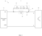
- a circuit system 1 of this embodiment includes the drive acceleration circuit 10 and a switching device 20.
- the switching device 20 has a control end G.
- the drive acceleration circuit 10 is electrically connected to the control end G of the switching device 20 to output a drive signal, thereby driving the switching device 20 to turn on or turn off.
- the switching device 20 is an insulated gate bipolar transistor, and the control end G is a gate of the insulated gate bipolar transistor.
- the drive acceleration circuit 10 includes a drive power supply 11, a basic drive unit 12, a drive acceleration unit 13, and a selective conduction unit 14.
- the basic drive unit 12 constitutes a first drive tributary 15, and the drive acceleration unit 13 and the selective conduction unit 14 serve as a second drive tributary 16 after being connected in series.
- the first drive tributary 15 and the second drive tributary 16 are configured to: when closed, provide a charging and discharging path for the switching device 20.
- the drive acceleration unit 13 and the selective conduction unit 14 are connected in series, and then connected to the basic drive unit 12 in parallel. In other words, the first drive tributary 15 and the second drive tributary 16 are connected in parallel.
- the drive power supply 11 has an output end OUT and a signal reference end GND.
- the output end OUT is configured to output a drive signal
- the signal reference end GND is configured to output a reference signal that serves as a reference ground.
- the switching device 20 further includes a connection end E.
- the connection end is an emitter.
- the connection end E may alternatively be a collector.
- the signal reference end GND is electrically connected to the connection end E.
- the drive signal output by the output end OUT is applied to the control end G of the switching device 20.
- the selective conduction unit 14 is configured to control a working status of the second drive tributary 16.
- the second drive tributary 16 is controlled by the selective conduction unit 14 to be in a closed or open state.
- the drive acceleration unit 13 is included in the drive acceleration circuit 10 or excluded from the drive acceleration circuit 10. (In other words, the drive acceleration unit 13 is connected to the drive acceleration circuit 10 or disconnected from the drive acceleration circuit 10.)
- the drive signal is a pulse signal.
- a first state for example, a high level state, such as 15V
- the switching device 20 is driven to turn on.
- the drive signal is in a second state (for example, at a low level, such as -5V)
- the switching device 20 is driven to turn off.
- the selective conduction unit 14 controls the working status of the second drive tributary 16, so that the drive acceleration unit 13 is included in the turn-on delay period T 1 and the turn-off delay period T 4 of the switching device 20; and the selective conduction unit 14 controls the working status of the second drive tributary 16, so that the drive acceleration unit 13 is excluded in the turn-on action period T 2 and the turn-off action period T 5 of the switching device 20.
- the selective conduction unit 14 controls the second drive tributary 16 to be in a closed state in the turn-on delay period T 1 and the turn-off delay period T 4 of the switching device 20; and the selective conduction unit 14 controls the second drive tributary 16 to be in an open state in the turn-on action period T 2 and the turn-off action period T 5 of the switching device 20.
- the basic drive unit 12 and the drive acceleration unit 13 include one of or any combination of a resistor, a capacitor, and a diode. There is one or more resistors, capacitors, and diodes. The one or more resistors, capacitors, and diodes may be connected in series or in parallel.
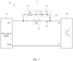
- the basic drive unit 12 includes a first resistor R1
- the drive acceleration unit 13 includes a second resistor R2 and a capacitor C
- the selective conduction unit 14 includes a first zener diode Vzi and a second zener diode V Z2 .
- the second resistor R2, the capacitor C, the first zener diode V Z1 , and the second zener diode V Z2 . are consecutively connected in series.
- the second resistor R2 is further electrically connected to the output end OUT of the drive power supply 11.
- the second zener diode V Z2 is further electrically connected to the control end G of the switching device 20.
- a negative electrode of the first zener diode Vzi is electrically connected to the output end OUT of the drive power supply 11, and a positive electrode of the first zener diode Vzi is electrically connected to the switching device 20.
- a positive electrode of the second zener diode V Z2 is electrically connected to the output end OUT of the drive power supply 11, and a negative electrode of the second zener diode V Z2 is electrically connected to the switching device 20.
- the first resistor R1 is electrically connected between the output end OUT of the drive power supply 11 and the control end G of the switching device 20, and is connected in parallel with the second resistor R2, the capacitor C, the first zener diode V Z1 , and the second zener diode V Z2 .
- a working principle of the circuit system 1 shown in FIG. 4 is illustrated by using an example in which a threshold voltage of the switching device 20 is 5 V, and breakdown voltages of the first zener diode Vzi and the second zener diode V Z2 are 10V
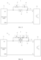
- the drive signal is in a high level (+15V) state in the turn-on delay period T 1 .
- a voltage V G of the control end G of the switching device 20 gradually increases from -5V to the threshold voltage of +5V (which is a miller plateau of the switching device 20 in this embodiment).
- the first zener diode Vzi enters a reverse breakdown state, with a working voltage of 10V
- the second zener diode V Z2 enters a forward conduction state, and acts as a diode.
- both the first drive tributary 15 and the second drive tributary 16 are in a closed state.
- the second resistor R2 and the capacitor C can provide a sufficient gate drive peak current. In this way, the switching device 20 is charged by using the first drive tributary 15, and the charging is accelerated by using the second drive tributary 16, to accelerate a turn-on delay process of the switching device 20.
- a voltage V G of the control end G has reached the threshold voltage of +5V of the switching device in the turn-on action period Tz.
- the switching device 20 is turned on, and the first zener diode Vzi in the selective conduction unit 14 is cut off, so that the second drive tributary 16 is in an open state.
- only the first drive tributary 15 is closed, and the switching device 20 is charged only by using the first drive tributary 15. Therefore, a charging speed is reduced in comparison with that in the turn-on delay period, and a small current change rate is maintained for the switching device 20, thereby avoiding a risk of stress.
- the first drive tributary 15 constantly stays in a closed state
- the second drive tributary 16 constantly stays in an open state.
- the voltage V G of the control end G has exceeded +5V and the switching device 20 has been turned on, to prevent the switching device 20 from being erroneously turned off due to fluctuation of the drive signal, a high level of the drive signal needs to be greater than +5V Therefore, the voltage V G of the control end G continues to increase to +15V after reaching the miller plateau.
- the drive signal is in a low level (-5V) state in the turn-off delay period T 4 .
- a voltage of the control end G of the switching device 20 gradually decreases from +15V to +5V
- the first zener diode Vzi enters a forward conduction state and acts as a diode.
- the second zener diode V Z2 enters a reverse breakdown state, with a working voltage of 10V
- both the first drive tributary 15 and the second drive tributary 16 are in a closed state.
- the second resistor R2 and the capacitor C can provide a discharging path that has a low impedance, to accelerate a turn-off delay process of the switching device 20. Refer to FIG. 8 .
- the second zener diode V Z2 is cut off in the turn-off action period T 5 , so that the second drive tributary 16 is in an open state. At this time, only the first drive tributary 15 is closed, and the switching device 20 is discharged only by using the first drive tributary 15. A discharging speed is reduced, and a small current change rate is maintained for the switching device 20, thereby avoiding a risk of stress.
- the voltage V G of the control end G is already greater than +5V in a period following the turn-off action period T 5 of the switching device 20 and the switching device 20 has been turned off, to prevent the switching device 20 from being erroneously turned on due to fluctuation of the drive signal, a low level of the drive signal needs to be less than +5V Therefore, the voltage V G of the control end G continues to decrease to -5V after decreasing to less than +5V.
- a voltage V G of the control end G may not be + 15V during normal operation of the switching device 20, and a voltage V G of the control end G may not be -5V when the switching device 20 is turned off.
- the foregoing voltage values in this embodiment are merely intended for illustrative description.
- the drive acceleration unit 13 accelerates normal turn-on delay and turn-off delay processes in the turn-on delay period T 1 and the turn-off delay period T 4 , but does not accelerate normal turn-on and turn-off processes of the switching device 20.
- a corresponding zener diode (Vzi or V Z2 ) in the selective conduction unit 14 is cut off, to control the second drive tributary 16 in which the drive acceleration unit 13 is located to be in an open state, so that charging and discharging processes of the switching device 20 are not accelerated, achieving a stable current change rate for the switching device 20.
- This can effectively suppress a voltage spike and reduce a risk of stress to the switching device 20, thereby solving the foregoing technical problem that stress of the switching device 20 is prone to increase when the drive signal has a small pulse width.
- zener diodes V Z1 and V Z2 with matching working voltages need to be selected based on the threshold voltage of the switching device 20 and the high level and the low level of the drive signal.
- turn-on and turn-off speeds of the switching device 20 are related to values of the capacitor C, the first resistor R1, and the second resistor R2.
- a capacitor C with a specific capacitance value and a first resistor R1 and a second resistor R2 with specific resistance values may be selected to achieve specific turn-on and turn-off speeds.
- a larger capacitance value and a smaller resistance value mean larger charging and discharging currents and faster charging and discharging speeds of the switching device 20.
- a smaller capacitance value and a larger resistance value mean smaller charging and discharging currents and slower charging and discharging speeds of the switching device 20.
- a resistance value of the first resistor R1 is greater than a resistance value of the second resistor R2.
- the first zener diode Vzi and/or the second zener diode V Z2 may alternatively be replaced by another semiconductor device such as a transient voltage suppressor (Transient Voltage Suppressor, TVS) or a switching device.
- circuit structures of the basic drive unit 12 and the drive acceleration unit 13 may alternatively be different, provided that a charging and discharging path can be provided.
- the first zener diode Vzi is made to enter a reverse breakdown state in the turn-on delay period T 1 of the switching device 20 and to be cut off in the turn-on action period T 2 , thereby controlling the drive acceleration unit 13 to be included in the drive acceleration circuit 10 or excluded from the drive acceleration circuit 10.
- the second zener diode V Z2 is made to enter a reverse breakdown state in the turn-off delay period T 4 of the switching device 20 and to be cut off in the turn-off action period T 5 , thereby controlling the drive acceleration unit 13 to be included in the drive acceleration circuit 10 or excluded from the drive acceleration circuit 10.
- the selective conduction unit 14 includes the first zener diode Vzi or the second zener diode V Z2 , rather than including the first zener diode Vzi and the second zener diode V Z2 .
- the selective conduction unit 14 may include only one of the first zener diode Vzi and the second zener diode V Z2 . For example, refer to FIG. 9 .
- the selective conduction unit 14 When the selective conduction unit 14 includes the first zener diode Vzi, the selective conduction unit 14 is configured to control a working status of the second drive tributary 16 in a turn-on process (including the turn-on delay period T 1 and the turn-on action period T 2 ) of the switching device 20. For example, refer to FIG. 10 .
- the selective conduction unit 14 includes the second zener diode V Z2
- the selective conduction unit 14 is configured to control a working status of the second drive tributary 16 in a turn-off process (including the turn-off delay period T 4 and the turn-off action period T 5 ) of the switching device 20.
- the selective conduction unit 14 includes only one of the first zener diode Vzi and the second zener diode V Z2 . This is conducive to meeting requirements of switching devices 20 in different circuit systems.
- the drive acceleration unit 13 does not include a capacitor C.
- a resistance value of the second resistor R2 is far less than a resistance value of the first resistor R1. Therefore, charging and discharging currents of the second drive tributary 16 are far greater than charging and discharging currents of the first drive tributary 15, and the switching device 20 can be rapidly charged and discharged by using the second drive tributary 16, thereby achieving rapid turn-on or turn-off.
- selective conduction unit 14 may include only one of the first zener diode Vzi and the second zener diode V Z2 , as shown in FIG. 8 and FIG. 10 . Details are not described herein again.
- the circuit system 1 of this embodiment includes the drive acceleration circuit 10.
- the drive acceleration circuit 10 includes the selective conduction unit 14.
- the selective conduction unit 14 is configured to control the drive acceleration unit 13 to be in a closed state in the turn-on delay period T 1 and the turn-off delay period T 4 , to shorten the turn-on delay period T 1 and the turn-off delay period T 4 .
- the selective conduction unit 14 is further configured to control the drive acceleration unit 13 to be in an open state in the turn-on action period T 2 and the turn-off action period T 5 , so that the turn-on action period T 2 and the turn-off action period T 5 are not shortened.
- the drive acceleration circuit 10 implements selective acceleration of charging and discharging processes of the switching device 20.
- a main difference of a circuit system 2 in this embodiment from the circuit system 1 in the embodiments shown in FIG. 4 to FIG. 10 lies in that a drive acceleration unit 13 in a second drive tributary 16 further includes a third resistor R3.
- the third resistor R3 is connected in series with a second resistor R2, and the third resistor R3 is connected in parallel with a capacitor C.
- a resistance value of the third resistor R3 is far greater than resistance values of a first resistor R1 and the second resistor R2, and the resistance value of the second resistor R2 is less than the resistance value of the first resistor R1.
- the capacitor C and the third resistor R3 are included in the second drive tributary 16 in a time division manner.
- the switching device 20 in a turn-on delay period T 1 , is charged by using a first drive tributary 15 and the second drive tributary 16. Specifically, the switching device 20 is charged by using the second resistor R2 and the capacitor C in the second drive tributary 16, so that the drive acceleration unit 13 accelerates a turn-on process of the switching device 20 in the turn-on delay period T 1 .
- a turn-on action period T 2 the capacitor C in the drive acceleration unit 13 has been charged to a specific voltage.
- a path including the second resistor R2 and the third resistor R3 is closed.
- a total resistance value of the second drive tributary 16 is a sum of the resistance values of the second resistor R2 and the third resistor R3, and is far greater than the resistance value of the first resistor R1 in the first drive tributary 15.
- a resistance value on the second drive tributary 16 is far greater than a resistance value on the first drive tributary 15.
- a charging current on the second drive tributary 16 is far smaller than a charging current on the first drive tributary 15.
- the switching device 20 is mainly charged by using the first drive tributary 15.
- a current change rate is small, so that normal turn-on of the switching device 20 is not affected.
- a drive signal is jumped to a low level, and the switching device 20 starts to perform discharging.
- both the first drive tributary 15 and the second drive tributary 16 are closed.
- the switching device 20 is discharged by using the second resistor R2 and the capacitor C in the second drive tributary 16, so that the drive acceleration unit 13 accelerates a discharging process of the switching device 20 in the turn-off delay period T 4 .
- a turn-off action period T 5 the capacitor C in the drive acceleration unit 13 is in an open state.
- a path including the second resistor R2 and the third resistor R3 is closed, and the switching device 20 is also charged and discharged by using the first drive tributary 15 and the second drive tributary 16.
- the switching device 20 is charged and discharged by using the second resistor R2 and the third resistor R3 in the second drive tributary 16.
- a total resistance value of the second drive tributary 16 is far greater than a total resistance value of the first drive tributary 15. Therefore, a discharging current of the first drive tributary 15 is far greater than a discharging current of the second drive tributary 16.
- the switching device 20 is mainly discharged by using the first drive tributary 15.
- a current change rate is small, so that normal turn-off of the switching device 20 is not affected.
- the capacitor C can be excluded from the second drive tributary 16, so that the third resistor R3 is included, in place of the capacitor C, in the second drive tributary 16. Therefore, this can also effectively improve turn-on and turn-off speeds of the switching device 20.
- the selective conduction unit 14 may include only one of the first zener diode Vzi and the second zener diode V Z2 , similar to the embodiments shown in FIG. 9 and FIG. 10 . Details are not described herein again.
- the circuit system 2 and a drive acceleration circuit 10 of this embodiment can achieve all beneficial effects described in Embodiment 1.
- a charging/discharging status of the capacitor C may be further used to control the second drive tributary 16 to be included or excluded.
- a main difference of a circuit system 3 in this embodiment from the circuit system 1 in Embodiment 1 and the circuit system 2 in Embodiment 2 lies in that a drive acceleration circuit 10 includes at least two second drive tributaries 16.
- the second drive tributaries 16 are connected with each other in parallel.
- two second drive tributaries 16 are included.
- the second drive tributaries 16 work in a time division manner. When closed, the second drive tributaries 16 have different charging/discharging currents.
- second resistors R2 with different resistance values or/and capacitors C with different capacitance values are selected, so that the second drive tributaries 16 have different charging/discharging currents when closed.
- a first zener diode Vzi and a second zener diode V Z2 in the selective conduction unit 14 have different breakdown voltages, so that the second drive tributaries 16 are closed in a time division manner. In other words, the second drive tributaries 16 are not closed at the same time.
- the two second drive tributaries 16 are controlled, by using the selective conduction unit 14 in each second drive tributary 16, to be closed in a time division manner.
- the switching device 20 has different charging/discharging speeds in sub-periods of the turn-on delay period T 1 and the turn-off delay period T 4 .
- a charging/discharging current when the second drive tributary 16 is closed may be set, to control charging/discharging speeds of the switching device 20 in the sub-periods of the turn-on delay period T 1 and the turn-off delay period T 4 to gradually decrease, until a charging/discharging speed at a miller plateau is reached.
- each second drive tributary 16 may be the same as a structure of any second drive tributary 16 described in Embodiment 1 and Embodiment 2, for example, structures in examples shown in FIG. 18 and FIG. 19 . Details are not described herein again.
- the circuit system 3 and the drive acceleration circuit 10 of this embodiment can achieve all beneficial effects described in Embodiment 1 and Embodiment 2.
- the switching device 20 may further be controlled to have gradient charging/discharging speeds in turn-on and turn-off processes.
Landscapes
- Engineering & Computer Science (AREA)
- Power Engineering (AREA)
- Electronic Switches (AREA)
- Power Conversion In General (AREA)
Abstract
Description
- This application relates to the field of electronic circuit technologies, and in particular, to a drive acceleration circuit and a circuit system.
- Semiconductor switching devices such as insulated gate bipolar transistors (IIGBT), metal-oxide-semiconductor field-effect transistors (MOSFET), and new-type wide bandgap semiconductors (including wide bandgap semiconductor materials such as SiC and GaN) are widely applied in electronic circuits. In some application scenarios, to reduce conduction losses of a switching device, a switching device with a slow switching speed is considered. However, the switching device is also expected to operate in a highly frequent on/off switching state. In this case, a drive acceleration circuit is required to ensure that a slow semiconductor switching device has highly frequent on/off switching capabilities. However, in some cases, the drive acceleration circuit causes the switching device to turn off abruptly. This greatly increases stress, posing stress risks to the switching device.
- A first aspect of this application provides a drive acceleration circuit, configured to drive a switching device to turn on or turn off. The switching device has a control end and a connection end. The drive acceleration circuit includes: a drive power supply, including an output end and a reference signal end, where the output end is configured to output a drive signal, and the reference signal end is electrically connected to the connection end of the switching device and is configured to output a reference signal to the connection end; a first drive tributary, where the first drive tributary is electrically connected to the output end of the drive power supply and the control end of the switching device, and is configured to drive, based on the drive signal, the switching device to turn on or turn off; and a second drive tributary, which is connected in parallel with the first drive tributary, where the second drive tributary includes a drive acceleration unit and a selective conduction unit, one end of the drive acceleration unit is electrically connected to the output end of the drive power supply, another end of the drive acceleration unit is electrically connected to the control end of the switching device through the selective conduction unit, the selective conduction unit is turned on in a time division manner to make the second drive tributary closed or open, and the drive acceleration unit is configured to accelerate on/off of the switching device based on the drive signal when the second drive tributary is closed.
- The drive acceleration circuit includes the first drive tributary and the second drive tributary. The first drive tributary is configured to drive the switching device to turn on or turn off. The second drive tributary includes the drive acceleration unit and the selective conduction unit. The selective conduction unit may control the second drive tributary to be closed or open, so that the drive acceleration unit in the second drive tributary is included in the drive acceleration circuit or excluded from the drive acceleration circuit. When included in the drive acceleration circuit, the drive acceleration unit is also configured to drive the switching device to turn on or turn off. Based on a working characteristic of the switching device, in some specific working periods of the switching device, when the drive acceleration unit drives the switching device, a turn-on speed or a turn-off speed of the switching device may be accelerated. However, in some other specific working periods of the switching device, the drive acceleration unit may cause a current of the switching device to change excessively rapidly, increasing stress. Therefore, a switch control circuit is disposed in the drive acceleration circuit to control a working status (closed or open) of the second drive tributary, thereby controlling the drive acceleration unit to be included in some specific periods and excluded in some other specific periods. In this way, in addition to improving turn-on and turn-off speeds of the switching device, the drive acceleration circuit further avoids a risk of increasing stress of the switching device.
- In some embodiments, the selective conduction unit includes at least one semiconductor device, one end of the at least one semiconductor device is connected to the drive acceleration unit, another end of the at least one semiconductor device is connected to the control end of the switching device, and the at least one semiconductor device is turned on or off in a time division manner to make the second drive tributary closed or open.
- In some embodiments, the at least one semiconductor device is a zener diode, a transient voltage suppressor, or a switching device.
- In this way, the semiconductor device (a zener diode, a transient voltage suppressor, or a switching device) is disposed. This is conducive to controlling the second drive tributary to be closed or open.
- In some embodiments, the selective conduction unit includes two semiconductor devices, and either of the semiconductor devices is a zener diode or a transient voltage suppressor. Anodes of the two semiconductor devices are electrically connected to each other, a cathode of one semiconductor device is electrically connected to the drive acceleration unit, and a cathode of the other semiconductor device is electrically connected to the control end of the switching device.
- In this way, connection directions of the two semiconductor devices are opposite to each other. Driven by drive signals of different directions, the two semiconductor devices enter a conduction or reverse cutoff state, so that the drive acceleration unit in the second drive tributary can be included in the drive acceleration circuit in both turn-on and turn-off processes of the switching device. This is conducive to both accelerating a turn-on process of the switching device and accelerating a turn-off process of the switching device.
- In some embodiments, the drive acceleration circuit includes at least two second drive tributaries that are connected in parallel, and the at least two second drive tributaries are closed in a time division manner.
- In this way, a turn-on process and/or a turn-off process of the switching device can be accelerated in a time division manner by using a plurality of second drive tributaries.
- In some embodiments, the second drive tributaries are of the same structure.
- This is conducive to calculating and selecting a parameter (such as a resistance value or a capacitance value) of a corresponding component in each second drive tributary.
- In some embodiments, the second drive tributaries have different resistance values.
- In this way, a turn-on process and/or a turn-off process of the switching device can be accelerated at different speeds in different periods by controlling the second drive tributaries to be closed in a time division manner.
- In some embodiments, the second drive tributary is configured to be in a closed state when the switching device is in a turn-off delay period, and to be in an open state when the switching device is in a turn-off action period; or the second drive tributary is configured to be in a closed state both when the switching device is in a turn-off delay period and when the switching device is in a turn-off action period.
- In this way, when the second drive tributary is closed in the turn-off delay period and is open in the turn-off action period, this is conducive to shortening the turn-off delay period of the switching device without affecting the turn-off action period of the switching device, thereby further avoiding increasing stress of the switching device while reducing a turn-off delay of the switching device.
- In some embodiments, the second drive tributary is configured to be in a closed state when the switching device is in a turn-on delay period, and to be in an open state when the switching device is in a turn-on action period; or the second drive tributary is configured to be in a closed state both when the switching device is in a turn-on delay period and when the switching device is in a turn-on action period.
- In this way, when the second drive tributary is closed in the turn-on delay period and is open in the turn-on action period, this is conducive to shortening the turn-on delay period of the switching device without shortening the turn-on action period of the switching device, thereby further avoiding increasing stress of the switching device while accelerating a turn-on process of the switching device.
- In some embodiments, the drive acceleration unit includes any one or combination of a resistor, a capacitor, and a diode, one end of one of the resistor, the capacitor, and the diode or one end of any combination of the resistor, the capacitor, and the diode that are connected in series or parallel is electrically connected to the output end of the drive power supply, and another end thereof is electrically connected to the selective conduction unit.
- In this way, a charging and discharging path can be provided in the turn-on delay period and the turn-off delay period of the switching device.
- In some embodiments, the first drive tributary includes a first resistor, one end of the first resistor is connected to the output end of the drive power supply, and another end of the first resistor is connected to the control end of the switching device; and
the drive acceleration unit includes a second resistor, where one end of the second resistor is connected to the output end of the drive power supply, and another end of the second resistor is connected to the selective conduction unit. - In this way, a current of the first drive tributary remains less than a current of the second drive tributary when the second drive tributary is closed. When the second drive tributary is closed, a turn-on delay or/and a turn-off delay is reduced. When the first drive tributary is closed, a current change rate of the switching device remains normal in turn-on and turn-off processes.
- In some embodiments, the drive acceleration unit further includes a capacitor that is connected in series with the second resistor, the one end of the second resistor is connected to the output end of the drive power supply, the another end of the second resistor is connected to the capacitor, another end of the capacitor is connected to the selective conduction unit, and the capacitor is configured to perform charging or discharging when the second drive tributary is closed.
- This is conducive to improving a current on the second drive tributary in charging and discharging processes of the capacitor, thereby reducing a turn-on delay and/or a turn-off delay of the switching device.
- In some embodiments, the drive acceleration unit further includes a third resistor, the third resistor is connected in parallel with the capacitor, one end of the third resistor is connected to the second resistor, another end of the third resistor is connected to the selective conduction unit, and the third resistor and the capacitor are included in the second drive tributary in a time division manner.
- In this way, when the capacitor is included in the second drive tributary, the second drive tributary has a large current, thereby accelerating on or/and off of the switching device. When the third resistor is included in the second drive tributary, the second drive tributary has a small current, so that the switching device can normally turn on and turn off without being affected, thereby avoiding a risk of generating stress.
- In some embodiments, a sum of the resistance value of the second resistor and a resistance value of the third resistor is greater than the resistance value of the first resistor.
- In this way, when the third resistor is included in the second drive tributary, a current on the second drive tributary is less than a current on the first drive tributary. The switching device performs charging and discharging mainly by using the first drive tributary. The switching device can maintain a relatively small current change rate during normal turn-on and turn-off action periods. This is conducive to avoiding a risk of stress.
- A second aspect of this application provides a circuit system, including: a switching device, which has a control end and a connection end; and the drive acceleration circuit according to any one of the foregoing embodiments, where the drive acceleration circuit is electrically connected to the control end and the connection end of the switching device, and is configured to drive on/off of the switching device.
- The circuit system includes the drive acceleration circuit, and the drive acceleration circuit includes a first drive tributary and a second drive tributary. The first drive tributary is configured to drive the switching device to turn on or turn off. The second drive tributary includes a drive acceleration unit and a selective conduction unit. The selective conduction unit may control the second drive tributary to be closed or open, so that the drive acceleration unit in the second drive tributary is included in the drive acceleration circuit or excluded from the drive acceleration circuit. When included in the drive acceleration circuit, the drive acceleration unit is also configured to drive the switching device to turn on or turn off. Based on a working characteristic of the switching device, in some specific working periods of the switching device, when the drive acceleration unit drives the switching device, a turn-on speed or a turn-off speed of the switching device may be accelerated. However, in some other specific working periods of the switching device, the drive acceleration unit may cause a current of the switching device to change excessively rapidly, increasing stress. Therefore, a switch control circuit is disposed in the drive acceleration circuit to control a working status (closed or open) of the second drive tributary, thereby controlling the drive acceleration unit to be included in some specific periods and excluded in some other specific periods. In this way, in addition to improving turn-on and turn-off speeds of the switching device, the circuit system and the drive acceleration circuit further avoid a risk of increasing stress of the switching device.
-
-
FIG. 1 is a schematic diagram of an I-V curve of a switching device when a drive power supply outputs a drive signal with a large pulse; -
FIG. 2 is a schematic diagram of an I-V curve of a switching device when a drive power supply outputs a drive signal with a small pulse; -
FIG. 3 is a schematic diagram of a modular structure of a circuit system according toEmbodiment 1 of this application; -
FIG. 4 is a schematic diagram of a circuit structure of a circuit system according toEmbodiment 1 of this application; -
FIG. 5 is a schematic diagram of a structure of an equivalent circuit of the circuit system inFIG. 4 in a turn-on delay period of a switching device; -
FIG. 6 is a schematic diagram of a structure of an equivalent circuit of the circuit system inFIG. 4 in a turn-on action period of a switching device; -
FIG. 7 is a schematic diagram of a structure of an equivalent circuit of the circuit system inFIG. 4 in a turn-off delay period of a switching device; -
FIG. 8 is a schematic diagram of a structure of an equivalent circuit of the circuit system inFIG. 4 in a turn-off action period of a switching device; -
FIG. 9 is a schematic diagram of a circuit structure of a circuit system according to a variant embodiment ofEmbodiment 1 of this application; -
FIG. 10 is a schematic diagram of a circuit structure of a circuit system according to another variant embodiment ofEmbodiment 1 of this application; -
FIG. 11 is a schematic diagram of a circuit structure of a circuit system according to another variant embodiment ofEmbodiment 1 of this application; -
FIG. 12 is a schematic diagram of a circuit structure of a circuit system according to another variant embodiment ofEmbodiment 1 of this application; -
FIG. 13 is a schematic diagram of a circuit structure of a circuit system according to another variant embodiment ofEmbodiment 1 of this application; -
FIG. 14 is a schematic diagram of a circuit structure of a circuit system according toEmbodiment 2 of this application; -
FIG. 15 is a schematic diagram of a circuit structure of a circuit system according to a variant embodiment ofEmbodiment 2 of this application; -
FIG. 16 is a schematic diagram of a circuit structure of a circuit system according to another variant embodiment ofEmbodiment 2 of this application; -
FIG. 17 is a schematic diagram of a circuit structure of a circuit system according toEmbodiment 3 of this application; -
FIG. 18 is a schematic diagram of a circuit structure of a circuit system according to a variant embodiment ofEmbodiment 3 of this application; and -
FIG. 19 is a schematic diagram of a circuit structure of a circuit system according to another variant embodiment ofEmbodiment 3 of this application. -
Circuit system 1, 2, and 3 Drive acceleration circuit 10 Drive power supply 11 Output end out Basic drive unit 12 Drive acceleration unit 13 Selective conduction unit 14 First drive tributary 15 Second drive tributary 16 First resistor R1 Second resistor R2 Third resistor R3 Capacitor C First zener diode VZ1 Second zener diode VZ2 Switching device 20 Control end G Connection end E Reference signal end GND Period T1, T2, T4, and T5 - The following describes embodiments of this application with reference to accompanying drawings of embodiments of this application.
- It should be noted that when an element is considered to "be connected" to another element, it may be directly connected to the another element, or an element disposed in between may coexist. When one or more elements or units are considered to "constitute" or "serve as" another element, it only indicates that the relationship exists in the described embodiment.
- Unless otherwise specified, all the technical and scientific terms used in this specification have the same meanings as those generally understood by technical personnel in the technical field of this application. Terms used in this specification of this application are merely intended for the purpose of describing specific embodiments rather than limiting this application. The term "and/or" used in this specification includes any and all combinations of one or more associated items that are listed.
- This application provides a circuit system that includes a drive acceleration circuit and a switching device. The circuit system is applied to a drive circuit of a semiconductor switching device. The drive acceleration circuit is configured to drive the switching device to turn on and turn off. In this application, the switching device is a semiconductor switching device, for example, an insulated gate bipolar transistor, a metal-oxide-semiconductor field-effect transistor, or a new-type wide bandgap semiconductor. The switching device has a control end. The drive acceleration circuit outputs a drive signal to the control end of the switching device, to drive the switching device to turn on and turn off. In this application, for an I-V curve of an entire process in which the switching device starts to turn on until turn-off ends, refer to
FIG. 1 . InFIG. 1 , a horizontal coordinate indicates time, and a vertical coordinate indicates a voltage VG of the control end of the switching device. T1 is defined as a turn-on delay period of the switching device, T2 is defined as a turn-on action period of the switching device, T4 is defined as a turn-off delay period of the switching device, and T5 is defined as a turn-off action period of the switching device. At a moment when the period T5 ends, the switching device has been completely turned off. However, in a period following the period T5, VG still continues to drop, until VG reaches a low level (-5V) of the drive signal. - In this application, a threshold voltage of the switching device is +5V In other words, when the switching device reaches a miller plateau, a voltage VG at a gate is +5V In other words, when VG reaches +5 V, the switching device is turned on; and when VG is less than +5 V, the switching device is turned off. The voltage of the drive signal periodically jumps between +15V and -5V However, because of a working characteristic of the semiconductor switching device, VG of the switching device can hardly be switched instantaneously, but it takes some time to complete voltage switching. For example, in the turn-on delay period T1 of the switching device, VG gradually increases from -5V to +5V; and in the turn-off delay period T4 of the switching device, VG gradually decreases from +15V to +5V. Existence of the turn-on delay period T1 and the turn-off delay period T4 affects turn-on and turn-off speeds of the switching device.
- In this application, the
basic drive unit 12 is configured to drive the switching device to turn on or turn off. Thedrive acceleration unit 13 is configured to be turned on in the turn-on delay period T1 and the turn-off delay period T4 of the switching device, to shorten the turn-on delay period T1 and the turn-off delay period T4 of the switching device, thereby reducing a turn-on delay and a turn-off delay. - When a pulse width is large, an I-V curve of the switching device is shown in
FIG. 1 . - Refer to
FIG. 2 . When a pulse width of the drive signal is small, in some cases, when VG just reaches +5V, in other words, when the switching device is in the turn-on action period T2 and the switching device is just turned on, a level of the drive signal jumps from +15V to -5V, and the switching device immediately starts to turn off. If thedrive acceleration unit 13 drives the switching device at this time, the miller plateau is directly accelerated. This speeds up a normal turn-off process of the switching device, and a current change rate suddenly increases, greatly increasing stress of the switching device and causing a risk of stress to the switching device. - It can be learned that delays (the turn-on delay period T1 and the turn-off delay period T4) of specific duration exist both in turn-on and turn-off processes of the switching device. If the turn-on delay period T1 and the turn-off delay period T4 of the switching device are shortened, this is conducive to reducing turn-on and turn-off delays of the switching device, thereby speeding up turn-on and turn-off speeds. However, when the pulse width of the drive signal is small, the miller plateau of the switching device is consequently accelerated. In other words, the normal turn-on action period T2 and turn-off action period T5 of the switching device are also shortened. This brings a risk of increased stress.
- In this application, a drive signal whose pulse width is greater than a sum of the turn-on delay period T1 and the turn-on action period T2 of the switching device is defined as a drive signal with a large pulse, and a drive signal whose pulse width is less than or equal to a sum of the turn-on delay period T1 and the turn-on action period T2 of the switching device is defined as a drive signal with a small pulse.
- In this embodiment, a
drive acceleration circuit 10 performs acceleration in a turn-on delay period T1 and a turn-off delay period T4 of a switching device, and is disconnected in a turn-on action period T2 and a turn-off action period T5 of the switching device. This resolves the foregoing technical problem that "when the pulse width of the drive signal is small, stress of the switching device is consequently increased." - Refer to
FIG. 3 . Acircuit system 1 of this embodiment includes thedrive acceleration circuit 10 and aswitching device 20. In this embodiment, the switchingdevice 20 has a control end G. Thedrive acceleration circuit 10 is electrically connected to the control end G of theswitching device 20 to output a drive signal, thereby driving theswitching device 20 to turn on or turn off. In this embodiment, as an example for description, the switchingdevice 20 is an insulated gate bipolar transistor, and the control end G is a gate of the insulated gate bipolar transistor. Thedrive acceleration circuit 10 includes adrive power supply 11, abasic drive unit 12, adrive acceleration unit 13, and aselective conduction unit 14. In this embodiment, thebasic drive unit 12 constitutes afirst drive tributary 15, and thedrive acceleration unit 13 and theselective conduction unit 14 serve as asecond drive tributary 16 after being connected in series. Thefirst drive tributary 15 and thesecond drive tributary 16 are configured to: when closed, provide a charging and discharging path for theswitching device 20. Thedrive acceleration unit 13 and theselective conduction unit 14 are connected in series, and then connected to thebasic drive unit 12 in parallel. In other words, thefirst drive tributary 15 and thesecond drive tributary 16 are connected in parallel. - The
drive power supply 11 has an output end OUT and a signal reference end GND. The output end OUT is configured to output a drive signal, and the signal reference end GND is configured to output a reference signal that serves as a reference ground. The switchingdevice 20 further includes a connection end E. In this embodiment, the connection end is an emitter. In another embodiment, the connection end E may alternatively be a collector. The signal reference end GND is electrically connected to the connection end E. The drive signal output by the output end OUT is applied to the control end G of theswitching device 20. In this embodiment, theselective conduction unit 14 is configured to control a working status of thesecond drive tributary 16. In other words, thesecond drive tributary 16 is controlled by theselective conduction unit 14 to be in a closed or open state. In this way, thedrive acceleration unit 13 is included in thedrive acceleration circuit 10 or excluded from thedrive acceleration circuit 10. (In other words, thedrive acceleration unit 13 is connected to thedrive acceleration circuit 10 or disconnected from thedrive acceleration circuit 10.) - In this embodiment, the drive signal is a pulse signal. When the drive signal is in a first state (for example, a high level state, such as 15V), the switching
device 20 is driven to turn on. When the drive signal is in a second state (for example, at a low level, such as -5V), the switchingdevice 20 is driven to turn off. - In this embodiment, the
selective conduction unit 14 controls the working status of thesecond drive tributary 16, so that thedrive acceleration unit 13 is included in the turn-on delay period T1 and the turn-off delay period T4 of theswitching device 20; and theselective conduction unit 14 controls the working status of thesecond drive tributary 16, so that thedrive acceleration unit 13 is excluded in the turn-on action period T2 and the turn-off action period T5 of theswitching device 20. In other words, theselective conduction unit 14 controls thesecond drive tributary 16 to be in a closed state in the turn-on delay period T1 and the turn-off delay period T4 of theswitching device 20; and theselective conduction unit 14 controls thesecond drive tributary 16 to be in an open state in the turn-on action period T2 and the turn-off action period T5 of theswitching device 20. - The
basic drive unit 12 and thedrive acceleration unit 13 include one of or any combination of a resistor, a capacitor, and a diode. There is one or more resistors, capacitors, and diodes. The one or more resistors, capacitors, and diodes may be connected in series or in parallel. - Refer to
FIG. 4 . In this embodiment, thebasic drive unit 12 includes a first resistor R1, thedrive acceleration unit 13 includes a second resistor R2 and a capacitor C, and theselective conduction unit 14 includes a first zener diode Vzi and a second zener diode VZ2. The second resistor R2, the capacitor C, the first zener diode VZ1, and the second zener diode VZ2.are consecutively connected in series. The second resistor R2 is further electrically connected to the output end OUT of thedrive power supply 11. The second zener diode VZ2 is further electrically connected to the control end G of theswitching device 20. In this embodiment, a negative electrode of the first zener diode Vzi is electrically connected to the output end OUT of thedrive power supply 11, and a positive electrode of the first zener diode Vzi is electrically connected to theswitching device 20. A positive electrode of the second zener diode VZ2 is electrically connected to the output end OUT of thedrive power supply 11, and a negative electrode of the second zener diode VZ2 is electrically connected to theswitching device 20. The first resistor R1 is electrically connected between the output end OUT of thedrive power supply 11 and the control end G of theswitching device 20, and is connected in parallel with the second resistor R2, the capacitor C, the first zener diode VZ1, and the second zener diode VZ2. - In this embodiment, a working principle of the
circuit system 1 shown inFIG. 4 is illustrated by using an example in which a threshold voltage of theswitching device 20 is 5 V, and breakdown voltages of the first zener diode Vzi and the second zener diode VZ2 are 10V - Refer to
FIG. 5 . The drive signal is in a high level (+15V) state in the turn-on delay period T1. When driven by the drive signal, a voltage VG of the control end G of theswitching device 20 gradually increases from -5V to the threshold voltage of +5V (which is a miller plateau of theswitching device 20 in this embodiment). At this time, the first zener diode Vzi enters a reverse breakdown state, with a working voltage of 10V The second zener diode VZ2 enters a forward conduction state, and acts as a diode. At this time, both thefirst drive tributary 15 and thesecond drive tributary 16 are in a closed state. In thesecond drive tributary 16, the second resistor R2 and the capacitor C can provide a sufficient gate drive peak current. In this way, the switchingdevice 20 is charged by using thefirst drive tributary 15, and the charging is accelerated by using thesecond drive tributary 16, to accelerate a turn-on delay process of theswitching device 20. - Refer to
FIG. 6 . A voltage VG of the control end G has reached the threshold voltage of +5V of the switching device in the turn-on action period Tz. At this time, the switchingdevice 20 is turned on, and the first zener diode Vzi in theselective conduction unit 14 is cut off, so that thesecond drive tributary 16 is in an open state. At this time, only thefirst drive tributary 15 is closed, and theswitching device 20 is charged only by using thefirst drive tributary 15. Therefore, a charging speed is reduced in comparison with that in the turn-on delay period, and a small current change rate is maintained for theswitching device 20, thereby avoiding a risk of stress. - During normal operation of the
switching device 20, thefirst drive tributary 15 constantly stays in a closed state, and thesecond drive tributary 16 constantly stays in an open state. Although the voltage VG of the control end G has exceeded +5V and theswitching device 20 has been turned on, to prevent theswitching device 20 from being erroneously turned off due to fluctuation of the drive signal, a high level of the drive signal needs to be greater than +5V Therefore, the voltage VG of the control end G continues to increase to +15V after reaching the miller plateau. Refer toFIG. 7 . The drive signal is in a low level (-5V) state in the turn-off delay period T4. When driven by the drive signal, a voltage of the control end G of theswitching device 20 gradually decreases from +15V to +5V At this time, the first zener diode Vzi enters a forward conduction state and acts as a diode. The second zener diode VZ2 enters a reverse breakdown state, with a working voltage of 10V At this time, both thefirst drive tributary 15 and thesecond drive tributary 16 are in a closed state. In thesecond drive tributary 16, the second resistor R2 and the capacitor C can provide a discharging path that has a low impedance, to accelerate a turn-off delay process of theswitching device 20. Refer toFIG. 8 . The second zener diode VZ2 is cut off in the turn-off action period T5, so that thesecond drive tributary 16 is in an open state. At this time, only thefirst drive tributary 15 is closed, and theswitching device 20 is discharged only by using thefirst drive tributary 15. A discharging speed is reduced, and a small current change rate is maintained for theswitching device 20, thereby avoiding a risk of stress. - Although the voltage VG of the control end G is already greater than +5V in a period following the turn-off action period T5 of the
switching device 20 and theswitching device 20 has been turned off, to prevent theswitching device 20 from being erroneously turned on due to fluctuation of the drive signal, a low level of the drive signal needs to be less than +5V Therefore, the voltage VG of the control end G continues to decrease to -5V after decreasing to less than +5V. - It should be understood that in another embodiment, a voltage VG of the control end G may not be + 15V during normal operation of the
switching device 20, and a voltage VG of the control end G may not be -5V when theswitching device 20 is turned off. The foregoing voltage values in this embodiment are merely intended for illustrative description. - It can be learned, from the foregoing working process of the
circuit system 1, that thedrive acceleration unit 13 accelerates normal turn-on delay and turn-off delay processes in the turn-on delay period T1 and the turn-off delay period T4, but does not accelerate normal turn-on and turn-off processes of theswitching device 20. When theswitching device 20 reaches the miller plateau, a corresponding zener diode (Vzi or VZ2) in theselective conduction unit 14 is cut off, to control thesecond drive tributary 16 in which thedrive acceleration unit 13 is located to be in an open state, so that charging and discharging processes of theswitching device 20 are not accelerated, achieving a stable current change rate for theswitching device 20. This can effectively suppress a voltage spike and reduce a risk of stress to theswitching device 20, thereby solving the foregoing technical problem that stress of theswitching device 20 is prone to increase when the drive signal has a small pulse width. - To accurately control the
second drive tributary 16 to be in an open state in the turn-on action period T2 and the turn-off action period T5 of the switching device 20 (namely when theswitching device 20 is at the miller plateau), zener diodes VZ1 and VZ2 with matching working voltages need to be selected based on the threshold voltage of theswitching device 20 and the high level and the low level of the drive signal. - In this embodiment, turn-on and turn-off speeds of the
switching device 20 are related to values of the capacitor C, the first resistor R1, and the second resistor R2. A capacitor C with a specific capacitance value and a first resistor R1 and a second resistor R2 with specific resistance values may be selected to achieve specific turn-on and turn-off speeds. A larger capacitance value and a smaller resistance value mean larger charging and discharging currents and faster charging and discharging speeds of theswitching device 20. A smaller capacitance value and a larger resistance value mean smaller charging and discharging currents and slower charging and discharging speeds of theswitching device 20. - In this embodiment, a resistance value of the first resistor R1 is greater than a resistance value of the second resistor R2. In this way, when the
second drive tributary 16 is open, and thefirst drive tributary 15 is used for charging and discharging, charging and discharging currents are small, and a current change rate is small. This is conducive to normal turn-on and turn-off of theswitching device 20, thereby reducing a risk of stress to theswitching device 20. In a variant embodiment, the first zener diode Vzi and/or the second zener diode VZ2 may alternatively be replaced by another semiconductor device such as a transient voltage suppressor (Transient Voltage Suppressor, TVS) or a switching device. In another variant embodiment, circuit structures of thebasic drive unit 12 and thedrive acceleration unit 13 may alternatively be different, provided that a charging and discharging path can be provided. - In this embodiment, by using a working characteristic of the first zener diode VZ1, the first zener diode Vzi is made to enter a reverse breakdown state in the turn-on delay period T1 of the
switching device 20 and to be cut off in the turn-on action period T2, thereby controlling thedrive acceleration unit 13 to be included in thedrive acceleration circuit 10 or excluded from thedrive acceleration circuit 10. Similarly, by using a working characteristic of the second zener diode VZ2, the second zener diode VZ2 is made to enter a reverse breakdown state in the turn-off delay period T4 of theswitching device 20 and to be cut off in the turn-off action period T5, thereby controlling thedrive acceleration unit 13 to be included in thedrive acceleration circuit 10 or excluded from thedrive acceleration circuit 10. - In another variant embodiment, the
selective conduction unit 14 includes the first zener diode Vzi or the second zener diode VZ2, rather than including the first zener diode Vzi and the second zener diode VZ2. In other words, in another variant embodiment, theselective conduction unit 14 may include only one of the first zener diode Vzi and the second zener diode VZ2. For example, refer toFIG. 9 . When theselective conduction unit 14 includes the first zener diode Vzi, theselective conduction unit 14 is configured to control a working status of thesecond drive tributary 16 in a turn-on process (including the turn-on delay period T1 and the turn-on action period T2) of theswitching device 20. For example, refer toFIG. 10 . When theselective conduction unit 14 includes the second zener diode VZ2, theselective conduction unit 14 is configured to control a working status of thesecond drive tributary 16 in a turn-off process (including the turn-off delay period T4 and the turn-off action period T5) of theswitching device 20. - In the variant embodiments shown in
FIG. 9 and FIG. 10 , theselective conduction unit 14 includes only one of the first zener diode Vzi and the second zener diode VZ2. This is conducive to meeting requirements of switchingdevices 20 in different circuit systems. - Refer to
FIG. 11 . In another variant embodiment, thedrive acceleration unit 13 does not include a capacitor C. In this variant embodiment, a resistance value of the second resistor R2 is far less than a resistance value of the first resistor R1. Therefore, charging and discharging currents of thesecond drive tributary 16 are far greater than charging and discharging currents of thefirst drive tributary 15, and theswitching device 20 can be rapidly charged and discharged by using thesecond drive tributary 16, thereby achieving rapid turn-on or turn-off. - Refer to
FIG. 12 andFIG. 13 . In a variant embodiment in which thedrive acceleration unit 13 does not include a capacitor C,selective conduction unit 14 may include only one of the first zener diode Vzi and the second zener diode VZ2, as shown inFIG. 8 andFIG. 10 . Details are not described herein again. - In summary, the
circuit system 1 of this embodiment includes thedrive acceleration circuit 10. Thedrive acceleration circuit 10 includes theselective conduction unit 14. Theselective conduction unit 14 is configured to control thedrive acceleration unit 13 to be in a closed state in the turn-on delay period T1 and the turn-off delay period T4, to shorten the turn-on delay period T1 and the turn-off delay period T4. Theselective conduction unit 14 is further configured to control thedrive acceleration unit 13 to be in an open state in the turn-on action period T2 and the turn-off action period T5, so that the turn-on action period T2 and the turn-off action period T5 are not shortened. In this way, thedrive acceleration circuit 10 implements selective acceleration of charging and discharging processes of theswitching device 20. This further accelerates normal turn-on and turn-off processes while ensuring shortened turn-on and turn-off delays. This effectively suppresses a voltage spike and reduces a risk of stress to theswitching device 20, thereby solving the foregoing technical problem that stress of the switching device is prone to increase when the drive signal has a small pulse width. - Refer to
FIG. 14 . A main difference of acircuit system 2 in this embodiment from thecircuit system 1 in the embodiments shown inFIG. 4 to FIG. 10 lies in that adrive acceleration unit 13 in asecond drive tributary 16 further includes a third resistor R3. The third resistor R3 is connected in series with a second resistor R2, and the third resistor R3 is connected in parallel with a capacitor C. In this embodiment, a resistance value of the third resistor R3 is far greater than resistance values of a first resistor R1 and the second resistor R2, and the resistance value of the second resistor R2 is less than the resistance value of the first resistor R1. In this embodiment, the capacitor C and the third resistor R3 are included in thesecond drive tributary 16 in a time division manner. - In this embodiment, in a turn-on delay period T1, the switching
device 20 is charged by using afirst drive tributary 15 and thesecond drive tributary 16. Specifically, the switchingdevice 20 is charged by using the second resistor R2 and the capacitor C in thesecond drive tributary 16, so that thedrive acceleration unit 13 accelerates a turn-on process of theswitching device 20 in the turn-on delay period T1. - In a turn-on action period T2, the capacitor C in the
drive acceleration unit 13 has been charged to a specific voltage. At this time, a path including the second resistor R2 and the third resistor R3 is closed. A total resistance value of thesecond drive tributary 16 is a sum of the resistance values of the second resistor R2 and the third resistor R3, and is far greater than the resistance value of the first resistor R1 in thefirst drive tributary 15. At this time, although both thefirst drive tributary 15 and thesecond drive tributary 16 are in a closed state, a resistance value on thesecond drive tributary 16 is far greater than a resistance value on thefirst drive tributary 15. Therefore, a charging current on thesecond drive tributary 16 is far smaller than a charging current on thefirst drive tributary 15. In other words, at this time, the switchingdevice 20 is mainly charged by using thefirst drive tributary 15. A current change rate is small, so that normal turn-on of theswitching device 20 is not affected. - In a turn-off delay period T4, a drive signal is jumped to a low level, and the
switching device 20 starts to perform discharging. At this time, both thefirst drive tributary 15 and thesecond drive tributary 16 are closed. Specifically, the switchingdevice 20 is discharged by using the second resistor R2 and the capacitor C in thesecond drive tributary 16, so that thedrive acceleration unit 13 accelerates a discharging process of theswitching device 20 in the turn-off delay period T4. - In a turn-off action period T5, the capacitor C in the
drive acceleration unit 13 is in an open state. At this time, a path including the second resistor R2 and the third resistor R3 is closed, and theswitching device 20 is also charged and discharged by using thefirst drive tributary 15 and thesecond drive tributary 16. Specifically, the switchingdevice 20 is charged and discharged by using the second resistor R2 and the third resistor R3 in thesecond drive tributary 16. A total resistance value of thesecond drive tributary 16 is far greater than a total resistance value of thefirst drive tributary 15. Therefore, a discharging current of thefirst drive tributary 15 is far greater than a discharging current of thesecond drive tributary 16. In other words, the switchingdevice 20 is mainly discharged by using thefirst drive tributary 15. A current change rate is small, so that normal turn-off of theswitching device 20 is not affected. - In other words, in this embodiment, even if the
second drive tributary 16 is not disconnected by theselective conduction unit 14, after the capacitor C is fully charged, the capacitor C can be excluded from thesecond drive tributary 16, so that the third resistor R3 is included, in place of the capacitor C, in thesecond drive tributary 16. Therefore, this can also effectively improve turn-on and turn-off speeds of theswitching device 20. - Refer to
FIG. 15 and FIG. 16 . In a variant embodiment of this embodiment, theselective conduction unit 14 may include only one of the first zener diode Vzi and the second zener diode VZ2, similar to the embodiments shown inFIG. 9 and FIG. 10 . Details are not described herein again. - In summary, the
circuit system 2 and adrive acceleration circuit 10 of this embodiment can achieve all beneficial effects described inEmbodiment 1. In addition, when thesecond drive tributary 16 is not disconnected by theselective conduction unit 14, a charging/discharging status of the capacitor C may be further used to control thesecond drive tributary 16 to be included or excluded. - Refer to
FIG. 17 . A main difference of acircuit system 3 in this embodiment from thecircuit system 1 inEmbodiment 1 and thecircuit system 2 inEmbodiment 2 lies in that adrive acceleration circuit 10 includes at least twosecond drive tributaries 16. Thesecond drive tributaries 16 are connected with each other in parallel. In this embodiment, as an example for description, twosecond drive tributaries 16 are included. - In this embodiment, the
second drive tributaries 16 work in a time division manner. When closed, thesecond drive tributaries 16 have different charging/discharging currents. In this embodiment, second resistors R2 with different resistance values or/and capacitors C with different capacitance values are selected, so that thesecond drive tributaries 16 have different charging/discharging currents when closed. In this embodiment, a first zener diode Vzi and a second zener diode VZ2 in theselective conduction unit 14 have different breakdown voltages, so that thesecond drive tributaries 16 are closed in a time division manner. In other words, thesecond drive tributaries 16 are not closed at the same time. - In this way, in a turn-on delay period T1 and a turn-off delay period T4, the two
second drive tributaries 16 are controlled, by using theselective conduction unit 14 in eachsecond drive tributary 16, to be closed in a time division manner. In this way, the switchingdevice 20 has different charging/discharging speeds in sub-periods of the turn-on delay period T1 and the turn-off delay period T4. For example, for eachsecond drive tributary 16, a charging/discharging current when thesecond drive tributary 16 is closed may be set, to control charging/discharging speeds of theswitching device 20 in the sub-periods of the turn-on delay period T1 and the turn-off delay period T4 to gradually decrease, until a charging/discharging speed at a miller plateau is reached. - In the
drive acceleration circuit 10 of this embodiment, a structure of eachsecond drive tributary 16 may be the same as a structure of anysecond drive tributary 16 described inEmbodiment 1 andEmbodiment 2, for example, structures in examples shown inFIG. 18 andFIG. 19 . Details are not described herein again. - The
circuit system 3 and thedrive acceleration circuit 10 of this embodiment can achieve all beneficial effects described inEmbodiment 1 andEmbodiment 2. In addition, the switchingdevice 20 may further be controlled to have gradient charging/discharging speeds in turn-on and turn-off processes. - A person with ordinary skills in the art should be aware that the foregoing implementations are merely intended for describing the present invention, rather than for limiting the present invention. Any appropriate modifications and changes made to the foregoing embodiments within the scope of the present invention shall fall within the protection scope claimed by the present invention.
Claims (15)
- A drive acceleration circuit, configured to drive a switching device to turn on or turn off, wherein the switching device has a control end and a connection end, and the drive acceleration circuit comprises:a drive power supply, comprising an output end and a reference signal end, wherein the output end is configured to output a drive signal, and the reference signal end is electrically connected to the connection end of the switching device and is configured to output a reference signal to the connection end;a first drive tributary, wherein the first drive tributary is electrically connected to the output end of the drive power supply and the control end of the switching device, and is configured to drive, based on the drive signal, the switching device to turn on or turn off; anda second drive tributary, which is connected in parallel with the first drive tributary, wherein the second drive tributary comprises a drive acceleration unit and a selective conduction unit, one end of the drive acceleration unit is electrically connected to the output end of the drive power supply, another end of the drive acceleration unit is electrically connected to the control end of the switching device through the selective conduction unit, the selective conduction unit is turned on in a time division manner to make the second drive tributary closed or open, and the drive acceleration unit is configured to accelerate on/off of the switching device based on the drive signal when the second drive tributary is closed.
- The drive acceleration circuit according to claim 1, wherein the selective conduction unit comprises at least one semiconductor device, one end of the at least one semiconductor device is connected to the drive acceleration unit, another end of the at least one semiconductor device is connected to the control end of the switching device, and the at least one semiconductor device is turned on or off in a time division manner to make the second drive tributary closed or open.
- The drive acceleration circuit according to claim 2, wherein the at least one semiconductor device is a zener diode, a transient voltage suppressor, or a switching device.
- The drive acceleration circuit according to claim 2 or 3, wherein the selective conduction unit comprises two semiconductor devices, and either of the semiconductor devices is a zener diode or a transient voltage suppressor; and
anodes of the two semiconductor devices are electrically connected to each other, a cathode of one semiconductor device is electrically connected to the drive acceleration unit, and a cathode of the other semiconductor device is electrically connected to the control end of the switching device. - The drive acceleration circuit according to any one of claims 1 to 4, wherein the drive acceleration circuit comprises at least two second drive tributaries that are connected in parallel, and the at least two second drive tributaries are closed in a time division manner.
- The drive acceleration circuit according to claim 5, wherein the second drive tributaries have different resistance values.
- The drive acceleration circuit according to any one of claims 1 to 6, whereinthe second drive tributary is configured to be in a closed state when the switching device is in a turn-off delay period, and to be in an open state when the switching device is in a turn-off action period; orthe second drive tributary is configured to be in a closed state both when the switching device is in a turn-off delay period and when the switching device is in a turn-off action period.
- The drive acceleration circuit according to any one of claims 1 to 7, whereinthe second drive tributary is configured to be in a closed state when the switching device is in a turn-on delay period, and to be in an open state when the switching device is in a turn-on action period; orthe second drive tributary is configured to be in a closed state both when the switching device is in a turn-on delay period and when the switching device is in a turn-on action period.
- The drive acceleration circuit according to any one of claims 1 to 8, wherein the drive acceleration unit comprises any one or combination of a resistor, a capacitor, and a diode, one end of one of the resistor, the capacitor, and the diode or one end of any combination of the resistor, the capacitor, and the diode that are connected in series or parallel is electrically connected to the output end of the drive power supply, and another end thereof is electrically connected to the selective conduction unit.
- The drive acceleration circuit according to claim 9, wherein the first drive tributary comprises a first resistor, one end of the first resistor is connected to the output end of the drive power supply, and another end of the first resistor is connected to the control end of the switching device; and
the drive acceleration unit comprises a second resistor, wherein one end of the second resistor is connected to the output end of the drive power supply, and another end of the second resistor is connected to the selective conduction unit. - The drive acceleration circuit according to claim 10, wherein a resistance value of the first resistor is greater than a resistance value of the second resistor.
- The drive acceleration circuit according to claim 11, wherein the drive acceleration unit further comprises a capacitor that is connected in series with the second resistor, the one end of the second resistor is connected to the output end of the drive power supply, the another end of the second resistor is connected to the capacitor, another end of the capacitor is connected to the selective conduction unit, and the capacitor is configured to perform charging or discharging when the second drive tributary is closed.
- The drive acceleration circuit according to claim 12, wherein the drive acceleration unit further comprises a third resistor, the third resistor is connected in parallel with the capacitor, one end of the third resistor is connected to the second resistor, another end of the third resistor is connected to the selective conduction unit, and the third resistor and the capacitor are comprised in the second drive tributary in a time division manner.
- The drive acceleration circuit according to claim 13, wherein a sum of the resistance value of the second resistor and a resistance value of the third resistor is greater than the resistance value of the first resistor.
- A circuit system, comprising:a switching device, which has a control end and a connection end; andthe drive acceleration circuit according to any one of claims 1 to 14, wherein the drive acceleration circuit is electrically connected to the control end and the connection end of the switching device, and is configured to accelerate an on/off process of the switching device.
Priority Applications (1)
| Application Number | Priority Date | Filing Date | Title |
|---|---|---|---|
| EP25213000.0A EP4716099A2 (en) | 2022-08-31 | 2023-08-30 | Drive acceleration circuit and circuit system |
Applications Claiming Priority (1)
| Application Number | Priority Date | Filing Date | Title |
|---|---|---|---|
| CN202211054162.4A CN115483814B (en) | 2022-08-31 | 2022-08-31 | Drive acceleration circuit and circuit system |
Related Child Applications (2)
| Application Number | Title | Priority Date | Filing Date |
|---|---|---|---|
| EP25213000.0A Division-Into EP4716099A2 (en) | 2022-08-31 | 2023-08-30 | Drive acceleration circuit and circuit system |
| EP25213000.0A Division EP4716099A2 (en) | 2022-08-31 | 2023-08-30 | Drive acceleration circuit and circuit system |
Publications (2)
| Publication Number | Publication Date |
|---|---|
| EP4333299A1 true EP4333299A1 (en) | 2024-03-06 |
| EP4333299B1 EP4333299B1 (en) | 2025-12-17 |
Family
ID=84421983
Family Applications (2)
| Application Number | Title | Priority Date | Filing Date |
|---|---|---|---|
| EP23194158.4A Active EP4333299B1 (en) | 2022-08-31 | 2023-08-30 | Drive acceleration circuit and circuit system |
| EP25213000.0A Pending EP4716099A2 (en) | 2022-08-31 | 2023-08-30 | Drive acceleration circuit and circuit system |
Family Applications After (1)
| Application Number | Title | Priority Date | Filing Date |
|---|---|---|---|
| EP25213000.0A Pending EP4716099A2 (en) | 2022-08-31 | 2023-08-30 | Drive acceleration circuit and circuit system |
Country Status (3)
| Country | Link |
|---|---|
| US (1) | US12525969B2 (en) |
| EP (2) | EP4333299B1 (en) |
| CN (1) | CN115483814B (en) |
Families Citing this family (1)
| Publication number | Priority date | Publication date | Assignee | Title |
|---|---|---|---|---|
| CN117595621A (en) * | 2023-11-09 | 2024-02-23 | 浙江极氪汽车研究开发有限公司 | An IGBT circuit, electric compressor, air conditioner and vehicle |
Citations (3)
| Publication number | Priority date | Publication date | Assignee | Title |
|---|---|---|---|---|
| WO2010132460A2 (en) * | 2009-05-11 | 2010-11-18 | Semisouth Laboratories, Inc. | Gate driver for enhancement-mode and depletion-mode wide bandgap semiconductor jfets |
| US20140055190A1 (en) * | 2011-06-09 | 2014-02-27 | Mitsubishi Electric Corporation | Gate drive circuit |
| JP2015204661A (en) * | 2014-04-11 | 2015-11-16 | 東芝シュネデール・インバータ株式会社 | Semiconductor element drive circuit |
Family Cites Families (7)
| Publication number | Priority date | Publication date | Assignee | Title |
|---|---|---|---|---|
| JP2002009598A (en) * | 2000-06-21 | 2002-01-11 | Mitsubishi Electric Corp | Voltage-controlled switching element drive circuit |
| JP2012147591A (en) * | 2011-01-13 | 2012-08-02 | Toyota Central R&D Labs Inc | Drive circuit |
| JP2013013044A (en) * | 2011-05-31 | 2013-01-17 | Sanken Electric Co Ltd | Gate drive circuit |
| CN103701323B (en) * | 2013-12-30 | 2016-06-15 | 成都芯源系统有限公司 | Switching power supply with constant on-time control, and control circuit and control method thereof |
| US9848467B2 (en) | 2014-05-30 | 2017-12-19 | Philips Lighting Holding B.V. | Driver for driving a load |
| CN113098240B (en) * | 2021-03-31 | 2024-01-16 | 西北工业大学 | A driving circuit for Cascode type GaN power devices |
| CN216774743U (en) * | 2021-10-29 | 2022-06-17 | 深圳青铜剑技术有限公司 | IGBT drive circuit |
-
2022
- 2022-08-31 CN CN202211054162.4A patent/CN115483814B/en active Active
-
2023
- 2023-08-30 US US18/239,871 patent/US12525969B2/en active Active
- 2023-08-30 EP EP23194158.4A patent/EP4333299B1/en active Active
- 2023-08-30 EP EP25213000.0A patent/EP4716099A2/en active Pending
Patent Citations (3)
| Publication number | Priority date | Publication date | Assignee | Title |
|---|---|---|---|---|
| WO2010132460A2 (en) * | 2009-05-11 | 2010-11-18 | Semisouth Laboratories, Inc. | Gate driver for enhancement-mode and depletion-mode wide bandgap semiconductor jfets |
| US20140055190A1 (en) * | 2011-06-09 | 2014-02-27 | Mitsubishi Electric Corporation | Gate drive circuit |
| JP2015204661A (en) * | 2014-04-11 | 2015-11-16 | 東芝シュネデール・インバータ株式会社 | Semiconductor element drive circuit |
Also Published As
| Publication number | Publication date |
|---|---|
| EP4333299B1 (en) | 2025-12-17 |
| EP4716099A2 (en) | 2026-03-25 |
| CN115483814B (en) | 2026-04-07 |
| US20240072784A1 (en) | 2024-02-29 |
| CN115483814A (en) | 2022-12-16 |
| US12525969B2 (en) | 2026-01-13 |
Similar Documents
| Publication | Publication Date | Title |
|---|---|---|
| US10554202B2 (en) | Gate driver | |
| US11611339B2 (en) | Power switch drive circuit and device | |
| US8558587B2 (en) | Gate driver | |
| US9755639B2 (en) | Device and method for an electronic circuit having a driver and rectifier | |
| US20190393871A1 (en) | Cascode switches including normally-off and normally-on devices and circuits comprising the switches | |
| US10622986B2 (en) | Gate voltage control circuit of insulated gate bipolar transistor and control method thereof | |
| AU2020388721B2 (en) | Driver circuit of power conversion device and application device thereof | |
| US20180375508A1 (en) | Power switching apparatus | |
| US20050206438A1 (en) | Drive circuit for voltage driven type semiconductor element | |
| US9154125B2 (en) | Method of controlling an IGBT and a gate driver | |
| US20160134279A1 (en) | Method and circuit for recharging a bootstrap capacitor using a transfer capacitor | |
| JP2003069401A (en) | Semiconductor power converter | |
| US9972992B2 (en) | Protection circuit of semiconductor device | |
| EP4333299A1 (en) | Drive acceleration circuit and circuit system | |
| US12334917B2 (en) | Voltage-source gate drive having shunt capacitors and shunt resistors | |
| US11637552B2 (en) | Driver circuit and switch system | |
| US20210111714A1 (en) | High-voltage fast switching devices | |
| US11824526B2 (en) | Circuit and control method for preventing false turn-on of semiconductor switching device | |
| US11115017B2 (en) | Driving apparatus and switching apparatus | |
| US12126329B2 (en) | Driving circuit | |
| JP2020096444A (en) | Switching circuit | |
| US20230308098A1 (en) | Current Sourced, Voltage Clamped, High Speed MOSFET Driver | |
| US12212224B2 (en) | Driving apparatus | |
| US20250392116A1 (en) | Short circuit protection of power switches | |
| US20180340972A1 (en) | Pulse current application circuit and control method thereof |
Legal Events
| Date | Code | Title | Description |
|---|---|---|---|
| PUAI | Public reference made under article 153(3) epc to a published international application that has entered the european phase |
Free format text: ORIGINAL CODE: 0009012 |
|
| STAA | Information on the status of an ep patent application or granted ep patent |
Free format text: STATUS: REQUEST FOR EXAMINATION WAS MADE |
|
| 17P | Request for examination filed |
Effective date: 20230830 |
|
| AK | Designated contracting states |
Kind code of ref document: A1 Designated state(s): AL AT BE BG CH CY CZ DE DK EE ES FI FR GB GR HR HU IE IS IT LI LT LU LV MC ME MK MT NL NO PL PT RO RS SE SI SK SM TR |
|
| STAA | Information on the status of an ep patent application or granted ep patent |
Free format text: STATUS: EXAMINATION IS IN PROGRESS |
|
| 17Q | First examination report despatched |
Effective date: 20250221 |
|
| GRAP | Despatch of communication of intention to grant a patent |
Free format text: ORIGINAL CODE: EPIDOSNIGR1 |
|
| STAA | Information on the status of an ep patent application or granted ep patent |
Free format text: STATUS: GRANT OF PATENT IS INTENDED |
|
| INTG | Intention to grant announced |
Effective date: 20250725 |
|
| GRAS | Grant fee paid |
Free format text: ORIGINAL CODE: EPIDOSNIGR3 |
|
| GRAA | (expected) grant |
Free format text: ORIGINAL CODE: 0009210 |
|
| STAA | Information on the status of an ep patent application or granted ep patent |
Free format text: STATUS: THE PATENT HAS BEEN GRANTED |
|
| AK | Designated contracting states |
Kind code of ref document: B1 Designated state(s): AL AT BE BG CH CY CZ DE DK EE ES FI FR GB GR HR HU IE IS IT LI LT LU LV MC ME MK MT NL NO PL PT RO RS SE SI SK SM TR |
|
| REG | Reference to a national code |
Ref country code: CH Ref legal event code: F10 Free format text: ST27 STATUS EVENT CODE: U-0-0-F10-F00 (AS PROVIDED BY THE NATIONAL OFFICE) Effective date: 20251217 Ref country code: GB Ref legal event code: FG4D |
|
| REG | Reference to a national code |
Ref country code: DE Ref legal event code: R096 Ref document number: 602023009766 Country of ref document: DE |
|
| REG | Reference to a national code |
Ref country code: LT Ref legal event code: MG9D |
|
| PG25 | Lapsed in a contracting state [announced via postgrant information from national office to epo] |
Ref country code: NO Free format text: LAPSE BECAUSE OF FAILURE TO SUBMIT A TRANSLATION OF THE DESCRIPTION OR TO PAY THE FEE WITHIN THE PRESCRIBED TIME-LIMIT Effective date: 20260317 |
|
| PG25 | Lapsed in a contracting state [announced via postgrant information from national office to epo] |
Ref country code: HR Free format text: LAPSE BECAUSE OF FAILURE TO SUBMIT A TRANSLATION OF THE DESCRIPTION OR TO PAY THE FEE WITHIN THE PRESCRIBED TIME-LIMIT Effective date: 20251217 Ref country code: FI Free format text: LAPSE BECAUSE OF FAILURE TO SUBMIT A TRANSLATION OF THE DESCRIPTION OR TO PAY THE FEE WITHIN THE PRESCRIBED TIME-LIMIT Effective date: 20251217 |
|
| PG25 | Lapsed in a contracting state [announced via postgrant information from national office to epo] |
Ref country code: RS Free format text: LAPSE BECAUSE OF FAILURE TO SUBMIT A TRANSLATION OF THE DESCRIPTION OR TO PAY THE FEE WITHIN THE PRESCRIBED TIME-LIMIT Effective date: 20260317 |
|
| REG | Reference to a national code |
Ref country code: NL Ref legal event code: MP Effective date: 20251217 |
|
| PG25 | Lapsed in a contracting state [announced via postgrant information from national office to epo] |
Ref country code: LV Free format text: LAPSE BECAUSE OF FAILURE TO SUBMIT A TRANSLATION OF THE DESCRIPTION OR TO PAY THE FEE WITHIN THE PRESCRIBED TIME-LIMIT Effective date: 20251217 |