EP4332783A1 - Time division multiplexing hub - Google Patents
Time division multiplexing hub Download PDFInfo
- Publication number
- EP4332783A1 EP4332783A1 EP23191304.7A EP23191304A EP4332783A1 EP 4332783 A1 EP4332783 A1 EP 4332783A1 EP 23191304 A EP23191304 A EP 23191304A EP 4332783 A1 EP4332783 A1 EP 4332783A1
- Authority
- EP
- European Patent Office
- Prior art keywords
- primary
- sensor
- data
- sensor device
- clock signal
- Prior art date
- Legal status (The legal status is an assumption and is not a legal conclusion. Google has not performed a legal analysis and makes no representation as to the accuracy of the status listed.)
- Pending
Links
Images


Classifications
-
- H—ELECTRICITY
- H04—ELECTRIC COMMUNICATION TECHNIQUE
- H04J—MULTIPLEX COMMUNICATION
- H04J3/00—Time-division multiplex systems
- H04J3/02—Details
- H04J3/06—Synchronising arrangements
- H04J3/0635—Clock or time synchronisation in a network
- H04J3/0685—Clock or time synchronisation in a node; Intranode synchronisation
-
- G—PHYSICS
- G06—COMPUTING OR CALCULATING; COUNTING
- G06F—ELECTRIC DIGITAL DATA PROCESSING
- G06F13/00—Interconnection of, or transfer of information or other signals between, memories, input/output devices or central processing units
- G06F13/14—Handling requests for interconnection or transfer
- G06F13/36—Handling requests for interconnection or transfer for access to common bus or bus system
- G06F13/368—Handling requests for interconnection or transfer for access to common bus or bus system with decentralised access control
- G06F13/372—Handling requests for interconnection or transfer for access to common bus or bus system with decentralised access control using a time-dependent priority, e.g. individually loaded time counters or time slot
-
- H—ELECTRICITY
- H04—ELECTRIC COMMUNICATION TECHNIQUE
- H04J—MULTIPLEX COMMUNICATION
- H04J3/00—Time-division multiplex systems
- H04J3/02—Details
- H04J3/06—Synchronising arrangements
- H04J3/0635—Clock or time synchronisation in a network
- H04J3/0638—Clock or time synchronisation among nodes; Internode synchronisation
- H04J3/0652—Synchronisation among time division multiple access [TDMA] nodes, e.g. time triggered protocol [TTP]
-
- G—PHYSICS
- G01—MEASURING; TESTING
- G01D—MEASURING NOT SPECIALLY ADAPTED FOR A SPECIFIC VARIABLE; ARRANGEMENTS FOR MEASURING TWO OR MORE VARIABLES NOT COVERED IN A SINGLE OTHER SUBCLASS; TARIFF METERING APPARATUS; MEASURING OR TESTING NOT OTHERWISE PROVIDED FOR
- G01D11/00—Component parts of measuring arrangements not specially adapted for a specific variable
-
- G—PHYSICS
- G01—MEASURING; TESTING
- G01D—MEASURING NOT SPECIALLY ADAPTED FOR A SPECIFIC VARIABLE; ARRANGEMENTS FOR MEASURING TWO OR MORE VARIABLES NOT COVERED IN A SINGLE OTHER SUBCLASS; TARIFF METERING APPARATUS; MEASURING OR TESTING NOT OTHERWISE PROVIDED FOR
- G01D21/00—Measuring or testing not otherwise provided for
-
- G—PHYSICS
- G06—COMPUTING OR CALCULATING; COUNTING
- G06F—ELECTRIC DIGITAL DATA PROCESSING
- G06F13/00—Interconnection of, or transfer of information or other signals between, memories, input/output devices or central processing units
- G06F13/38—Information transfer, e.g. on bus
- G06F13/40—Bus structure
- G06F13/4004—Coupling between buses
- G06F13/4022—Coupling between buses using switching circuits, e.g. switching matrix, connection or expansion network
-
- H—ELECTRICITY
- H04—ELECTRIC COMMUNICATION TECHNIQUE
- H04J—MULTIPLEX COMMUNICATION
- H04J3/00—Time-division multiplex systems
- H04J3/02—Details
- H04J3/06—Synchronising arrangements
- H04J3/0602—Systems characterised by the synchronising information used
- H04J3/0617—Systems characterised by the synchronising information used the synchronising signal being characterised by the frequency or phase
Definitions
- the present disclosure is related to sensor systems, and more particularly, to sensor systems that include a plurality of sensors.
- a sensor system may include a large number of individual sensors. Each sensor may output sensor data.
- a control circuit may receive the sensor data from each of the sensors. The control circuit may utilize the individual sensor data in order to generate overall sensor data or otherwise utilize the sensor signals to perform some other function.
- Time division multiplexing allows multiple channels of data to be transmitted on a single data line.
- each data source i.e. each individual sensor
- the timing frame corresponds to a selected number of clock cycles.
- the time window of each data source is a particular subset of the clock cycles of the timing frame.
- time division multiplexing can be an effective solution, there also serious difficulties associated with time division multiplexing.
- large numbers of data sources each with high data rates can lead to very high clock frequencies in order to enable data transmission. This can result in hard timing constraints for the sensors.
- very high frequencies rates can lead to high power consumption and difficulties in achieving electromagnetic compatibility.
- the present invention relates to a system and a method as defined in the annexed claims.
- Embodiments of the present disclosure provide a sensor system including a plurality of sensor devices and a control circuit operating in a time division multiplexing scheme.
- One of the sensor devices acts as a primary sensor device coupled directly to the control circuit.
- the remaining sensor devices are arranged in multiple groups of secondary sensor devices each connected to the primary sensor device. Each group provides sensor data to the primary sensor device in separate time division multiplexing schemes.
- the primary sensor device collects the sensor data from each group of secondary sensor devices and provides the sensor data from all of the secondary sensor devices and the sensor data from the primary sensor device in a single time division multiplexing arrangement to the control circuit.
- the use of a primary sensor device and multiple groups of secondary sensor devices provides various benefits.
- the separate time division multiplexing schemes enable the use of low clock frequencies between the primary sensor device and the groups of secondary sensor devices. This results in lower power consumption and more relaxed timing constraints. Accordingly, the efficiency and reliability of the sensor system is improved.
- While the present disclosure primarily describes the use of sensor devices in a time division multiplexing scheme, principles of the present disclosure can extend to other types of systems that include multiple data sources. Accordingly, principles of the present disclosure extend generally to systems that include multiple data sources that each output data to be aggregated in a time division multiplexing scheme.
- a system in one embodiment, includes a plurality of secondary sensor devices each configured to generate secondary sensor data.
- the system includes a primary sensor device coupled to each of the secondary sensor devices and configured to generate primary sensor data, to receive the secondary sensor data from each of the plurality of secondary sensor devices, and to output a data stream including the primary sensor data and the secondary sensor data from each secondary sensor device.
- the system includes a control device coupled to the primary sensor device and configured to receive the data stream from the primary sensor.
- a system in one embodiment, includes a first secondary sensor device including a first secondary slave circuit and a second secondary sensor device including a second secondary slave circuit.
- the system includes a primary sensor device including a first secondary master circuit coupled to the first secondary slave circuit, a second secondary master circuit coupled to the second secondary slave circuit, and a primary slave circuit.
- the system includes a control device including a primary master circuit coupled to the primary slave circuit and the first and second secondary master circuits.
- a method in one embodiment, includes generating primary sensor data with a primary sensor device, generating first secondary sensor data with a first secondary device, and generating second secondary sensor data with a second secondary sensor of a second secondary sensor device.
- the method includes controlling the primary sensor device with a primary master circuit of a control device coupled to the primary sensor device, controlling the first secondary sensor with a first secondary master circuit of the primary sensor device, and controlling the second secondary sensor with a second secondary master circuit of the primary sensor device.
- a method includes receiving, at a primary sensor device, a primary clock signal from a control device, generating, at the primary sensor device, a first secondary clock signal having a frequency lower than a frequency of the primary clock signal, and generating, at the primary sensor device, a second secondary clock signal having a frequency lower than the frequency of the primary clock signal.
- the method includes outputting first secondary sensor data from a first secondary sensor device to the primary sensor device in accordance with the first secondary clock signal and outputting second secondary sensor data from a second secondary sensor device to the primary sensor device in accordance with the second secondary clock signal.
- the method includes outputting, from the primary sensor device to the control device, a data stream including the first secondary sensor data, the second secondary sensor data, and the primary sensor data in accordance with the primary clock signal.
- FIG. 1 is a block diagram of a sensor system 100, according to one embodiment.
- the sensor system 100 includes a control device 102, a primary sensor device 104, and a plurality of secondary sensor devices 106a-106d.
- the arrangement and configuration of the primary sensor device 104 and the secondary sensor devices 106 enable a reliable and efficient data delivery system.
- the term "sensor device” may correspond to a device that includes a sensor and additional circuitry.
- the sensor generates sensor signals.
- the additional circuitry can include circuitry that generates sensor data from the sensor signals, circuitry that receives signals from one or more devices, and circuitry that sends signals to one or more devices.
- the primary sensor device 104 and the secondary sensor devices 106 each include a respective physical sensor that senses a physical phenomenon and generates sensor signals.
- the primary sensor device 104 and the secondary sensor devices 106 each generate sensor data from the respective sensor signals. This can include performing signal processing operations on the sensor signals to convert analog sensor signals to digital sensor data.
- primary sensor data refers to sensor data generated by the primary sensor device 104.
- secondary sensor data corresponds to sensor data generated by the secondary sensor devices 106.
- the control device 102 is coupled to the primary sensor device 104. As will be set forth in more detail below, the control device 102 receives a data stream from the primary sensor device including the sensor data from the primary sensor device 104 and the secondary sensor devices 106 on a single data line. The sensor data from the various sensor devices is provided by the primary sensor device 104 to the control device 102 in a time division multiplexing scheme.
- the control device 102 includes a primary master circuit 110.
- the primary master circuit 110 outputs a primary clock signal PCLK to the primary sensor device 104.
- the primary master circuit 110 outputs a primary frame signal PFS to the primary sensor device 104.
- the primary master circuit 110 receives from the primary sensor device 104 a sensor data stream SDS on a single data line.
- the primary clock signal PCLK is a master clock signal for the entire sensor system 100.
- the primary clock signal PCLK has a relatively high frequency.
- the primary clock signal PCLK can have a frequency between 1 MHz and 5 GHz, though other frequencies can be utilized without departing from the scope of the present disclosure.
- the primary frame signal PFS indicates the beginning of a frame.
- a frame corresponds to a number of cycles of the primary clock signal PCLK.
- the frame is further divided into a plurality of channels. Each channel corresponds to a number of cycles of the primary clock signal PCLK. Each channel is assigned to one of the sensor devices 104, 106.
- a frame correspond to 20 cycles of the primary clock signal PCLK.
- the first channel corresponds to the first four clock cycles of the frame and is assigned to the sensor data of the primary sensor device 104.
- the second channel corresponds to the second for clock cycles (cycles 5-8) of the frame and is assigned to the secondary sensor device 106a.
- the third channel corresponds to clock cycles 9-12 of the frame and is assigned to the secondary sensor device 106b.
- the fourth channel corresponds to clock cycles 13-16 of the frame and is assigned to the secondary sensor device 106c.
- the fifth channel corresponds to the clock cycles 17-20 of the frame and is assigned to the secondary sensor device 106d.
- the sensor data stream SDS includes the sensor data from each of the sensor devices 104 and 106.
- the primary master circuit 110 receives the first four data values (bits of value 0 or 1) of the sensor data stream SDS as the sensor data from the primary sensor device 104.
- the primary master circuit 110 receives the next four data values as the sensor data from the secondary sensor device 106a, and so forth until the frame is complete and four data values have been received for each sensor device 104 and 106.
- a frame of 20 cycles and five channels of four cycles each is given by way of illustrative example. In practice, a frame can have different numbers of cycles and different numbers of channels, and channels can have different numbers of cycles without departing from the scope of the present disclosure.
- the primary sensor device 104 includes a primary slave circuit 112.
- the primary slave circuit 112 receives the primary clock signal PCLK, the primary frame signal PFS, and provides the sensor data stream SDS to the primary master circuit 110. Accordingly, the primary slave circuit 112 acts as a slave to the primary master circuit 110 in that the primary master circuit provides the clock signal PCLK and the frame signal PFS to the primary slave circuit 112, while the primary slave circuit 112 provides the sensor data stream to the primary master circuit 110.
- the primary sensor device 104 includes secondary master circuit 114a and a secondary master circuit 114b.
- the secondary master circuit 114a communicates with the secondary sensor devices 106a and 106b of the group 108a.
- the secondary master circuit 114a outputs a secondary clock signal SCLK1 and a secondary frame signal SFS1 to the secondary sensor devices 106a and 106b.
- the secondary master circuit 114a receives a secondary sensor data signal SSD1.
- the secondary clock signal SCLK1 is a clock signal with a lower frequency than the primary clock signal PCLK.
- the secondary clock signal SCLK1 has a frequency equal to the frequency of PCLK divided by the number of secondary master circuits 114 of the primary sensor device 104.
- the frequency of SCLK1 is equal to half the frequency of PCLK, though other frequencies can be utilized for SCLK1 without departing from the scope of the present disclosure.
- the secondary frame signal SFS 1 is a frame signal similar to the primary frame signal PFS.
- the secondary frame signal SFS1 indicates the beginning of a frame.
- the frame corresponds to a number of cycles of the secondary clock signal SCLK1.
- the frame is further divided into a plurality of channels. Each channel corresponds to a number of cycles of the secondary clock signal SCLK1.
- Each channel is assigned to one of the sensor 106a and 106b.
- a frame corresponds to 8 cycles of the secondary clock signal SCLK1.
- the remaining four clock cycles of the frame correspond to the second channel and are assigned to the secondary sensor device 106b.
- the group 108a includes more than two secondary sensor devices 106 and the frame and configuration of channels are different than described above.
- the secondary master circuit 114a is connected to only a single secondary sensor device 106. In this case, the entirety of the frame of SFS1 is assigned to the single secondary sensor device 106.
- Each secondary sensor device 106a includes a respective secondary slave circuit 116.
- the secondary slave circuits 116 of the group 108a each receive the secondary clock signal SCLK1 and the secondary frame signal SFS1 from the secondary master circuit 114a.
- the slave circuit 116 of the secondary sensor device 106a provides sensor data to SSD1 during the first channel of the frame defined by SFS1.
- the slave circuit 116 of the secondary sensor device 106b provides sensor data to SSD1 during the second channel of the frame defined by SFS 1.
- the secondary master circuit 114a receives the sensor data from the secondary sensor devices of the group 108a and the secondary sensor data stream SSD1 in a time division multiplexing scheme.
- the secondary master circuit 114b communicates with the secondary sensor devices 106c and 106d of the group 108d.
- the secondary master circuit 114b outputs a secondary clock signal SCLK2 and a secondary frame signal SFS2 to the secondary sensor devices 106c and 106d.
- the secondary master circuit 114b receives a secondary sensor data signal SSD2.
- the secondary clock signal SCLK2 is a clock signal with a lower frequency than the primary clock signal PCLK.
- the secondary clock signal SCLK2 has a frequency equal to the frequency of PCLK divided by the number of secondary master circuits 114 of the primary sensor device 104.
- the frequency of SCLK2 is equal to half the frequency of PCLK, though other frequencies can be utilized for SCLK2 without departing from the scope of the present disclosure.
- the frequency of the secondary clock signal SCLK2 is identical to the frequency of the secondary clock signal of SCLK1.
- the secondary frame signal SFS2 is a frame signal similar to the primary frame signal PFS.
- the secondary frame signal SFS2 indicates the beginning of a frame for the group 108b.
- the frame corresponds to a number of cycles of the secondary clock signal SCLK2.
- the frame is further divided into a plurality of channels. Each channel corresponds to a number of cycles of the secondary clock signal SCLK2.
- Each channel is assigned to one of the sensor 106c and 106d.
- a frame corresponds to 8 cycles of the secondary clock signal SCLK2.
- the remaining four clock cycles of the frame correspond to the second channel and are assigned to the secondary sensor device 106d.
- the group 108b includes more than two secondary sensor devices 106 and the frame and configuration of channels may be different than described above.
- the secondary master circuit 114b is connected to only a single secondary sensor device 106. In this case, the entirety of the frame of SFS2 is assigned to the single secondary sensor device 106.
- Each secondary sensor device 106 includes a respective secondary slave circuit 116.
- the secondary slave circuits 116 of the group 108b each receive the secondary clock signal SCLK2 and the secondary frame signal SFS2 from the secondary master circuit 114b.
- the slave circuit 116 of the secondary sensor device 106c provides sensor data to SSD2 during the first channel of the frame defined by SFS2.
- the slave circuit 116 of the secondary sensor device 106d provides sensor data to SSD1 during the second channel of the frame defined by SFS2.
- the secondary master circuit 114b receives the sensor data from the secondary sensor devices of the group 108b in the secondary sensor data stream SSD2 in a time division multiplexing scheme.
- the primary slave circuit 112 receives SSD1 from the secondary master circuit 114a and SSD2 from the secondary master circuit 114b.
- the primary slave circuit 112 utilizes time division multiplexing to combine the sensor data from SSD1 and SSD2 with the sensor data generated by the primary sensor device 104 and provides the sensor data stream SDS to the primary master circuit 110 of the control device 102, as described previously.
- the primary slave circuit 112 provides the signals PCLK and PFS to both of the secondary master circuits 114a and 114b.
- the secondary master circuits generates SCLK1 and SCLK2 based on PCLK.
- the secondary master circuits 114a and 114b generates SFS1 and SFS2 based on PFS.
- secondary master circuits 114a and 114b may include overlapping circuitry with each other and with the primary slave circuit 112.
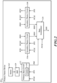
- FIG. 2 is a block diagram of a primary sensor device 104, in accordance with one embodiment.
- the primary sensor device 104 of Figure 2 is one example of a primary sensor device 104 of Figure 1 .
- the primary sensor device 104 includes a sensor 122.
- the sensor 122 can generate sensor signals indicative of a physical phenomenon being sensed.
- the sensor 122 can include a light sensor, a vibration sensor, an audio sensor, an inertial sensor, a voltage sensor, a current sensor, a temperature sensor, or other types of sensors.
- the sensor 122 outputs sensor signals indicative of the particular physical phenomenon being sensed.
- the sensor signals may initially be unprocessed analog sensor signals. Alternatively, sensor 122 can generate other types of sensor signals.
- the senor 122 is an inertial sensor including one or both of an accelerometer and a gyroscope.
- the sensor 122 includes one or both of a three-axis accelerometer and a three-axis gyroscope.
- the sensor signals include voltage or current signals indicative of acceleration and rotation on the various axes.
- the primary sensor device 104 includes a digital signal processor 120.
- the digital signal processor 120 receives the sensor signals from the sensor 122 and generates sensor data from the sensor signals. This can include converting analog sensor signals to digital sensor data.
- the digital signal processor 120 may include various types of circuitry that condition and otherwise process the sensor data.
- the primary sensor device 104 includes a primary slave circuit 112.
- the primary slave circuit 112 receives the signals PCLK and PFS from the primary master circuit 110, as described in relation to Figure 1 .
- the primary slave circuit 112 receives the primary sensor data sensor data from the DSP 120 and outputs the primary sensor data PSD.
- the primary slave circuit 112 includes a counter 124.
- the counter 124 counts the number of cycles of the CLK.
- the rising edge of PFS indicates the beginning of a frame.
- the counter Upon receiving the rising edge of PFS, the counter begins counting cycles of PCLK.
- the primary slave circuit 112 also includes a memory register stores configuration data for the primary slave circuit 112. The configuration data indicate which cycles of the frame are allocated to the channel corresponding to the primary sensor data PSD. The primary slave circuit 112 then output the primary sensor data on the clock cycles of PCLK assigned to the channel of the sensor 122 of the primary sensor device 104.
- the primary sensor device 104 includes the secondary master circuits 114a and 114b.
- the secondary master circuits 114a and 114b receive PCLK and PFS and output SFS1 and SCLK1 as described in relation to Figure 1 .
- the secondary master circuit 114a receives the secondary sensor data SSD1 and outputs the secondary sensor data SSD1.
- the secondary master circuit 114b outputs SCLK2 and SFS2 and receives SSD2 and outputs SSD2.
- the primary sensor device 104 includes a data accumulator 126.
- the data accumulator 126 is shown as separate from the primary slave circuit 112, the data accumulator 126 may be part of the primary slave circuit 112.
- the data accumulator 126 receives the signals PSD, SSD1, and SSD2, as well as PCLK.
- the data accumulator 126 generates the sensor data stream SDS and outputs the sensor data stream SDS to the primary master circuit 110.
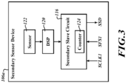
- FIG 3 is a block diagram of a secondary sensor device 106a, according to one embodiment.
- the secondary sensor device 106a is one example of a secondary sensor device 106a of Figure 1 . Additional secondary sensor devices are substantially identical to the secondary sensor device 106a.
- the secondary sensor device 106a includes a sensor 122.
- the sensor 122 can generate sensor signals indicative of a physical phenomenon being sensed.
- the sensor 122 can be a type of sensor described in relation to the sensor 122 of the primary sensor device 104 of Figure 2 . In one embodiment, all of the sensors 122 of the sensor devices 104 and 106 are a same type of sensor.
- the secondary sensor device 106a includes a digital signal processor 120.
- the digital signal processor 120 receives sensor signals from the sensor 122 and generate sensor data substantially as described in relation to the digital signal processor 120 of the primary sensor device 104 of Figure 2 .
- the secondary sensor device 106a includes a secondary slave circuit 116.
- the secondary slave circuit 116 receives the signals SCLK1 and SFS1 from the secondary master circuit 114a, as described in relation to Figure 1 .
- the secondary slave circuit 112 includes a counter 124.
- the counter 124 counts the number of cycles of SCLK1.
- the rising edge of SFS 1 indicates the beginning of a frame.
- the counter 124 begins counting cycles of SCLK1.
- the secondary slave circuit 116 also includes a memory or register that stores configuration data for the secondary slave circuit 116. The configuration data indicate which cycles of the frame are allocated to the channel corresponding to the secondary sensor device 106a.
- the secondary slave circuit 116 then outputs the secondary sensor data SSD on the clock cycles of SCLK1 assigned to the channel of the sensor 122 of secondary sensor device 106a.
- Each secondary slave circuit of the group 108a outputs secondary sensor data SSD in a time division multiplexing scheme to combine as SSD1.
- Each secondary slave circuit of the group 108B outputs secondary sensor data SSD in a time division multiplexing scheme to combine as SSD2.
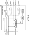
- FIG 4 is a schematic diagram of a primary sensor device 104, in accordance with one embodiment.
- the primary sensor device 104 is one example of a primary sensor device 104 of Figure 1 .
- the 104 includes input terminals that receive PFS, PCLK, SSD1, and SSD2.
- the primary sensor device 104 includes output terminals that provide SDS, SFS1, SCLK1, SFS2, and SCLK2.
- the primary sensor device 104 includes a delay circuit 130.
- the delay circuit 130 receives the primary frame signal PFS and generates the secondary frame signals SFS1 and SFS2.
- the secondary frame signals SFS1 and SFS2 are identical and correspond to the primary frame signal PFS delayed by a selected number of clock cycles of PCLK.
- the primary sensor device 104 includes a first clock divider 128a and the second clock divider 128b.
- the clock divider 128a receives the primary clock signal PCLK and generates the secondary clock signal SCLK1 by dividing the frequency of the primary clock signal PCLK in accordance with a selected division ratio.
- the clock divider 128b receives the primary clock signal PCLK and generates the secondary clock signal SCLK2 by dividing the frequency of the primary clock signal PCLK in accordance with a selected division ratio.
- the clock divider 128a, the delay circuit 130, the terminals that output SFS1 and a SCLK1, and the terminal that receives SSD1 are considered a secondary master circuit 114a.
- the clock divider 128b, the delay circuit 130, the terminals that output SFS2 and SCLK2, and the terminal that receives SSD2 are considered a secondary master circuit 114b.
- the secondary master circuits 114a and 114b share the delay circuit 130.
- the primary sensor device 104 may include a separate delay circuit 130 for each clock divider 128a/128b.
- the primary sensor device 104 includes the primary slave circuit 112, the digital signal processor 120, and the sensor 122 as described in relation to Figure 2 .
- the primary sensor device 104 also includes a shift register 132.
- the shift register 132 may be one example of a data accumulator 126 of Figure 2 .
- the shift register 132 receives the primary clock signal PCLK on a clock input terminal.
- the shift register 132 also receives the primary sensor data PSD, the secondary sensor data SSD1, and the secondary sensor data SSD2.
- the shift register outputs the sensor data stream SDS including the sensor data PSD, SSD1, and SSD2 all arranged in a time division-multiplexing scheme in accordance with the clock PCLK.
- Figure 4 illustrates the primary slave circuit 112 as separate from the shift register 132
- the primary slave circuit 112 can include the shift register 132, the terminals that receive PFS and PCLK, and the terminal the outputs SDS.
- Various configurations of a primary sensor device 104 and the primary slave circuit 112 can be utilized without departing from the scope of the present disclosure.
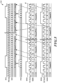
- Figure 5 is a graph 500 illustrating a plurality of sensor signals associated with a sensor system, in accordance with one embodiment.
- the example of Figure 5 corresponds to an embodiment in which there are N+1 sensor devices, where N is the total number of secondary sensor devices 106 and there is one primary sensor device 104.
- Each group 108 includes N/2 secondary sensor devices.
- the primary sensor device 104 includes more than two secondary master circuits 114.
- each group 108 has different numbers of secondary sensor devices.
- Figure 5 illustrates the primary frame signal PFS, the primary clock signal PCLK, and the sensor data stream SDS.
- the primary frame signal has a rising edge that indicates the beginning of a new frame.
- the primary clock signal PCLK is a clock signal substantially corresponding to a square wave.
- the primary clock signal PCLK is a relatively fast clock signal.
- the sensor data stream SDS is divided into channels. Each channel carries sensor data from a particular sensor device. Accordingly, there are N+1 channels in each frame.
- Figure 1 illustrates that each channel of the sensor data stream SDS includes four data values or bits.
- the sensor data stream SDS includes a data value for each cycle of the primary clock signal PCLK.
- each channel has four data values. However, in practice, each channel may have a larger number of data values or a smaller number of data values than shown in Figure 5 .
- Figure 5 illustrates the primary sensor data PSD.
- the primary sensor data PSD includes the sensor data generated by the sensor 122 of the primary sensor device 104.
- the primary sensor data PSD is included in channel 1 of the sensor data stream SDS.
- the primary sensor data PSD are in channels other than the first channel in a frame.
- the primary sensor data PSD be in a final channel of a frame.
- Figure 5 illustrates signals SFS1, SCLK1, and SSD1 associated with a first group 108a of secondary sensors.
- the first secondary frame signal SFS1 is delayed relative to the primary frame signal PFS.
- the delay is so large that the rising edge of SFS 1 is slightly before the rising edge of PFS.
- the secondary clock signal SCLK1 associated with the first group 108a of secondary sensors 106 has a lower frequency than the primary clock signal PCLK.
- Each data value in SSD1 has a width of one cycle of SCLK1.
- Each frame associated with SSD1 includes N/2 channels. There is one channel for each secondary sensor 106 in the group 108a of secondary sensors.
- FIG. 5 illustrates signals SFS2, SCLK2, and SSD2 associated with a second group 108b of secondary sensors 106.
- the second secondary frame signal SFS2 is delayed relative to the primary frame signal PFS.
- the delay is so large that the rising edge of SFS2 is slightly before the rising edge of PFS.
- the secondary clock signal SCLK2 associated with the first group 108b of secondary sensors 106 has a lower frequency than the primary clock signal PCLK.
- Each data value in SSD2 has a width of one cycle of SCLK2.
- Each frame associated with SSD2 includes N/2 channels. There is one channel for each secondary sensor 106 in the group 108a of secondary sensors.
- the primary sensor device 104 receives SSD1 and SSD2, and generates SDS from SSD1, SSD2 and SDS.
- the single channel associated with PSD is allocated to the first channel of SDS.
- Channel 1a of SSD1 is assigned to channel 2 of SDS.
- Channel 1b of SSD2 is assigned to channel 3 of SDS, and so forth until the data from each channel of SSD1 and SSD2 is placed in SDS.
- the data from PSD, SSD1, and SSD2 can be arranged into SDS by the data accumulator 126 of Figure 2 .
- the N secondary sensors can be operated with a relatively slow secondary clock signals.
- the secondary frames have a same duration as the primary frames, but are delayed relative to the primary frame signal. The result is that timing constraints are loosened and power consumption is reduced.
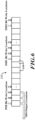
- FIG. 6 illustrates a shift register 132, according to one embodiment.
- the shift register 132 includes a plurality of data locations 140.
- the shift register 132 can operate like a first in first out (FIFO) buffer.
- the shift register 132 may operate in an unconventional manner in that data from PSD, SSD1, and SSD2 are inserted at different locations in the shift register 132.
- Switching devices can selectively enable data values from PSD, SSD1, and SSD2 to be inserted at their particular locations into the shift register. Once data is inserted, the switching devices can temporarily disable PSD, SSD1, and SSD2 from writing data into the shift register 132.
- the shift register 132 can then output SDS corresponding to a stream of data including channels from each of the primary and secondary sensor devices.
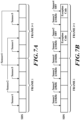
- FIG. 7A is a block diagram illustrating two frames of a sensor data stream SDS, according to one embodiment.
- each frame of SDS includes four channels, one for each sensor device.
- Sensors 2 and 4 may have slower data rates or may be disabled.
- Sensor 1 provides data for a first channel in frame i.
- Sensor 2 provides data for the second channel of frame i.
- Sensor 3 provides data for the third channel of frame i.
- Sensor 4 provides data for the fourth channel of frame i.
- Frame i+1 includes four channels, each assigned to a particular sensor. The frames repeat as long as the sensor system is generating sensor data. Accordingly, Figure 7A illustrates that in one embodiment if there are sensors with different data rates, or if there are sensors that have been disabled, data can be repeated for some of the sensors.
- FIG. 7B is a block diagram illustrating two frames of a sensor data stream SDS, according to one embodiment.
- each frame of SDS includes four channels, one for each sensor device.
- sensors 1 and 3 operate at higher clock speed than sensors 2 and 4. However, a same situation can occur when sensors 2 and 4 have been disabled.
- the solution can include resending the previous data.
- a solution is to send an exception code in the slots for which there is no data. This can enable the control circuit to ignore the slots that do not have valid data. This is illustrated in frame i+1 in which the channels assigned to sensor 2 and sensor 4 include an exception code indicating to the control circuit that these channels do not include valid data. Accordingly, Figure 7B illustrates that in one embodiment if there are sensors with different data rates, or if there are sensors that have been disabled, data can be transmitted as an exception code.
- FIG 8 is a block diagram of a sensor system 800, in accordance with some embodiments.
- the sensor system 800 of Figure 8 is substantially similar to the sensor system 100 of Figure 1 , except that there are N groups 108 and N secondary master circuits 1.
- Each group 108 includes one or more secondary sensor devices 108.
- Each secondary master circuit includes a frequency divider that provides a secondary clock signal to the corresponding group 108.
- Figure 8 shows only a single signal line between each secondary master circuit 114 and the corresponding group 108, in practice there is a signal line for each of the secondary clock signal, secondary frame signal, and secondary data stream, as shown in Figure 1 .
- each group 108 may include multiple secondary sensor devices or only a single secondary sensor device.
- the groups 108 may have differing numbers of secondary sensor devices 106.
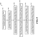
- Figure 9 is a flow diagram of a method 900 for operating a sensor system, in accordance with one embodiment.
- the method 900 can be implemented using systems, components, and processes described in relation to Figures 1-8 .
- the method 900 includes generating primary sensor data with a primary sensor device.
- the method 900 includes generating first secondary sensor data with a first secondary device.
- the method 900 includes generating second secondary sensor data with a second secondary sensor of a second secondary sensor device.
- the method 900 includes controlling the primary sensor device with a primary master circuit of a control device coupled to the primary sensor device.
- the method 900 includes controlling the first secondary sensor with a first secondary master circuit of the primary sensor device.
- the method 900 includes controlling the second secondary sensor with a second secondary master circuit of the primary sensor device.
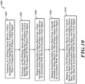
- Figure 10 is a flow diagram of a method 1000 for operating a sensor system, in accordance with one embodiment.
- the method 1000 can be implemented using systems, components, and processes described in relation to Figures 1-8 .
- the method 1000 includes generating, at a primary sensor device, a first secondary clock signal having a frequency lower than a frequency of a primary clock signal received by the primary sensor device from a control device.
- the method 1000 includes generating, at the primary sensor device, a second secondary clock signal having a frequency lower than the frequency of the primary clock signal.
- the method 1000 includes outputting first secondary sensor data from a first secondary sensor device to the primary sensor device in accordance with the first secondary clock signal.
- the method 1000 includes outputting second secondary sensor data from a second secondary sensor device to the primary sensor device in accordance with the second secondary clock signal.
- the method 1000 includes outputting, from the primary sensor device to the control device, a data stream including the first secondary sensor data, the second secondary sensor data, and the primary sensor data in accordance with the primary clock signal.
- a system in one embodiment, includes a plurality of secondary sensor devices each configured to generate secondary sensor data.
- the system includes a primary sensor device coupled to each of the secondary sensor devices and configured to generate primary sensor data, to receive the secondary sensor data from each of the plurality of secondary sensor devices, and to output a data stream including the primary sensor data and the secondary sensor data from each secondary sensor device.
- the system includes a control device coupled to the primary sensor device and configured to receive the data stream from the primary sensor.
- a system in one embodiment, includes a first secondary sensor device including a first secondary slave circuit and a second secondary sensor device including a second secondary slave circuit.
- the system includes a primary sensor device including a first secondary master circuit coupled to the first secondary slave circuit, a second secondary master circuit coupled to the second secondary slave circuit, and a primary slave circuit.
- the system includes a control device including a primary master circuit coupled to the primary slave circuit and the first and second secondary master circuits.
- a method in one embodiment, includes generating primary sensor data with a primary sensor device, generating first secondary sensor data with a first secondary device, and generating second secondary sensor data with a second secondary sensor of a second secondary sensor device.
- the method includes controlling the primary sensor device with a primary master circuit of a control device coupled to the primary sensor device, controlling the first secondary sensor with a first secondary master circuit of the primary sensor device, and controlling the second secondary sensor with a second secondary master circuit of the primary sensor device.
- a method includes receiving, at a primary sensor device, a primary clock signal from a control device, generating, at the primary sensor device, a first secondary clock signal having a frequency lower than a frequency of the primary clock signal, and generating, at the primary sensor device, a second secondary clock signal having a frequency lower than the frequency of the primary clock signal.
- the method includes outputting first secondary sensor data from a first secondary sensor device to the primary sensor device in accordance with the first secondary clock signal and outputting second secondary sensor data from a second secondary sensor device to the primary sensor device in accordance with the second secondary clock signal.
- the method includes outputting, from the primary sensor device to the control device, a data stream including the first secondary sensor data, the second secondary sensor data, and the primary sensor data in accordance with the primary clock signal.
Landscapes
- Engineering & Computer Science (AREA)
- Physics & Mathematics (AREA)
- Computer Networks & Wireless Communication (AREA)
- Signal Processing (AREA)
- General Physics & Mathematics (AREA)
- Theoretical Computer Science (AREA)
- General Engineering & Computer Science (AREA)
- Mathematical Physics (AREA)
- Computer Hardware Design (AREA)
- Arrangements For Transmission Of Measured Signals (AREA)
Abstract
Description
- The present disclosure is related to sensor systems, and more particularly, to sensor systems that include a plurality of sensors.
- A sensor system may include a large number of individual sensors. Each sensor may output sensor data. A control circuit may receive the sensor data from each of the sensors. The control circuit may utilize the individual sensor data in order to generate overall sensor data or otherwise utilize the sensor signals to perform some other function.
- It can be difficult to deliver the sensor data from each of the sensors to the control circuit in a manner that the control circuit can properly process the sensor data. One possible solution is to utilize time division multiplexing. Time division multiplexing allows multiple channels of data to be transmitted on a single data line. In time division multiplexing, each data source (i.e. each individual sensor) is assigned a time window within a specified timing frame. The timing frame corresponds to a selected number of clock cycles. The time window of each data source is a particular subset of the clock cycles of the timing frame.
- While time division multiplexing can be an effective solution, there also serious difficulties associated with time division multiplexing. In particular, large numbers of data sources each with high data rates can lead to very high clock frequencies in order to enable data transmission. This can result in hard timing constraints for the sensors. Furthermore, very high frequencies rates can lead to high power consumption and difficulties in achieving electromagnetic compatibility.
- All of the subject matter discussed in the Background section is not necessarily prior art and should not be assumed to be prior art merely as a result of its discussion in the Background section. Along these lines, any recognition of problems in the prior art discussed in the Background section or associated with such subject matter should not be treated as prior art unless expressly stated to be prior art. Instead, the discussion of any subject matter in the Background section should be treated as part of the inventor's approach to the particular problem, which, in and of itself, may also be inventive.
- The present invention relates to a system and a method as defined in the annexed claims.
- The present disclosure can be summarized as it follows.
- Embodiments of the present disclosure provide a sensor system including a plurality of sensor devices and a control circuit operating in a time division multiplexing scheme. One of the sensor devices acts as a primary sensor device coupled directly to the control circuit. The remaining sensor devices are arranged in multiple groups of secondary sensor devices each connected to the primary sensor device. Each group provides sensor data to the primary sensor device in separate time division multiplexing schemes. The primary sensor device collects the sensor data from each group of secondary sensor devices and provides the sensor data from all of the secondary sensor devices and the sensor data from the primary sensor device in a single time division multiplexing arrangement to the control circuit.
- The use of a primary sensor device and multiple groups of secondary sensor devices provides various benefits. The separate time division multiplexing schemes enable the use of low clock frequencies between the primary sensor device and the groups of secondary sensor devices. This results in lower power consumption and more relaxed timing constraints. Accordingly, the efficiency and reliability of the sensor system is improved.
- While the present disclosure primarily describes the use of sensor devices in a time division multiplexing scheme, principles of the present disclosure can extend to other types of systems that include multiple data sources. Accordingly, principles of the present disclosure extend generally to systems that include multiple data sources that each output data to be aggregated in a time division multiplexing scheme.
- In one embodiment, a system includes a plurality of secondary sensor devices each configured to generate secondary sensor data. The system includes a primary sensor device coupled to each of the secondary sensor devices and configured to generate primary sensor data, to receive the secondary sensor data from each of the plurality of secondary sensor devices, and to output a data stream including the primary sensor data and the secondary sensor data from each secondary sensor device. The system includes a control device coupled to the primary sensor device and configured to receive the data stream from the primary sensor.
- In one embodiment, a system includes a first secondary sensor device including a first secondary slave circuit and a second secondary sensor device including a second secondary slave circuit. The system includes a primary sensor device including a first secondary master circuit coupled to the first secondary slave circuit, a second secondary master circuit coupled to the second secondary slave circuit, and a primary slave circuit. The system includes a control device including a primary master circuit coupled to the primary slave circuit and the first and second secondary master circuits.
- In one embodiment, a method includes generating primary sensor data with a primary sensor device, generating first secondary sensor data with a first secondary device, and generating second secondary sensor data with a second secondary sensor of a second secondary sensor device. The method includes controlling the primary sensor device with a primary master circuit of a control device coupled to the primary sensor device, controlling the first secondary sensor with a first secondary master circuit of the primary sensor device, and controlling the second secondary sensor with a second secondary master circuit of the primary sensor device.
- In one embodiment, a method includes receiving, at a primary sensor device, a primary clock signal from a control device, generating, at the primary sensor device, a first secondary clock signal having a frequency lower than a frequency of the primary clock signal, and generating, at the primary sensor device, a second secondary clock signal having a frequency lower than the frequency of the primary clock signal. The method includes outputting first secondary sensor data from a first secondary sensor device to the primary sensor device in accordance with the first secondary clock signal and outputting second secondary sensor data from a second secondary sensor device to the primary sensor device in accordance with the second secondary clock signal. The method includes outputting, from the primary sensor device to the control device, a data stream including the first secondary sensor data, the second secondary sensor data, and the primary sensor data in accordance with the primary clock signal.
- Reference will now be made by way of example only to the accompanying drawings. In the drawings, identical reference numbers identify similar elements or acts. In some drawings, however, different reference numbers may be used to indicate the same or similar elements. The sizes and relative positions of elements in the drawings are not necessarily drawn to scale. For example, the shapes of various elements and angles are not necessarily drawn to scale, and some of these elements may be enlarged and positioned to improve drawing legibility.
-
Figure 1 is a block diagram of a sensor system, according to one embodiment. -
Figure 2 is a block diagram of a primary sensor device, according to one embodiment. -
Figure 3 is a block diagram of a secondary sensor device, according to one embodiment. -
Figure 4 is a schematic diagram of a primary sensor device, according to one embodiment. -
Figure 5 is a graph illustrating a plurality of signals associated with a sensor system, according to one embodiment. -
Figure 6 is a block diagram of a shift register, according to one embodiment. -
Figures 7A and 7B are block diagrams illustrating timings associated with sensor signals, according to one embodiment. -
Figure 8 is a block diagram of a sensor system, according to one embodiment. -
Figure 9 is a flow diagram of a method for operating a sensor system, according to one embodiment. -
Figure 10 is a flow diagram of a method for operating a sensor system according to one embodiment. - In the following description, certain specific details are set forth in order to provide a thorough understanding of various disclosed embodiments. However, one skilled in the relevant art will recognize that embodiments may be practiced without one or more of these specific details, or with other methods, components, materials, etc. In other instances, well-known systems, components, and circuitry associated with integrated circuits have not been shown or described in detail, to avoid unnecessarily obscuring descriptions of the embodiments.
- Unless the context requires otherwise, throughout the specification and claims which follow, the word "comprise" and variations thereof, such as, "comprises" and "comprising" are to be construed in an open, inclusive sense, that is as "including, but not limited to." Further, the terms "first," "second," and similar indicators of sequence are to be construed as interchangeable unless the context clearly dictates otherwise.
- Reference throughout this specification to "one embodiment" or "an embodiment" means that a particular feature, structure or characteristic described in connection with the embodiment is included in at least one embodiment. Thus, the appearances of the phrases "in one embodiment" or "in an embodiment" in various places throughout this specification are not necessarily all referring to the same embodiment. Furthermore, the particular features, structures, or characteristics may be combined in any suitable manner in one or more embodiments.
- As used in this specification and the appended claims, the singular forms "a," "an," and "the" include plural referents unless the content clearly dictates otherwise. It should also be noted that the term "or" is generally employed in its broadest sense, that is as meaning "and/or" unless the content clearly dictates otherwise.
-
Figure 1 is a block diagram of asensor system 100, according to one embodiment. Thesensor system 100 includes acontrol device 102, aprimary sensor device 104, and a plurality ofsecondary sensor devices 106a-106d. As will be set forth in more detail below, the arrangement and configuration of theprimary sensor device 104 and the secondary sensor devices 106 enable a reliable and efficient data delivery system. - As used herein, the term "sensor device" may correspond to a device that includes a sensor and additional circuitry. The sensor generates sensor signals. The additional circuitry can include circuitry that generates sensor data from the sensor signals, circuitry that receives signals from one or more devices, and circuitry that sends signals to one or more devices.
- The
primary sensor device 104 and the secondary sensor devices 106 each include a respective physical sensor that senses a physical phenomenon and generates sensor signals. Theprimary sensor device 104 and the secondary sensor devices 106 each generate sensor data from the respective sensor signals. This can include performing signal processing operations on the sensor signals to convert analog sensor signals to digital sensor data. As used herein the term "primary sensor data" refers to sensor data generated by theprimary sensor device 104. As used herein, the term "secondary sensor data" corresponds to sensor data generated by the secondary sensor devices 106. - The
control device 102 is coupled to theprimary sensor device 104. As will be set forth in more detail below, thecontrol device 102 receives a data stream from the primary sensor device including the sensor data from theprimary sensor device 104 and the secondary sensor devices 106 on a single data line. The sensor data from the various sensor devices is provided by theprimary sensor device 104 to thecontrol device 102 in a time division multiplexing scheme. - The
control device 102 includes aprimary master circuit 110. Theprimary master circuit 110 outputs a primary clock signal PCLK to theprimary sensor device 104. Theprimary master circuit 110 outputs a primary frame signal PFS to theprimary sensor device 104. Theprimary master circuit 110 receives from the primary sensor device 104 a sensor data stream SDS on a single data line. - The primary clock signal PCLK is a master clock signal for the
entire sensor system 100. The primary clock signal PCLK has a relatively high frequency. The primary clock signal PCLK can have a frequency between 1 MHz and 5 GHz, though other frequencies can be utilized without departing from the scope of the present disclosure. - The primary frame signal PFS indicates the beginning of a frame. A frame corresponds to a number of cycles of the primary clock signal PCLK. The frame is further divided into a plurality of channels. Each channel corresponds to a number of cycles of the primary clock signal PCLK. Each channel is assigned to one of the
sensor devices 104, 106. As an illustrative example, a frame correspond to 20 cycles of the primary clock signal PCLK. There are five sensor devices (oneprimary sensor device 104 and four secondary sensor devices 106). Accordingly, the frame is divided into five channels. Each channel corresponds to four clock cycles of the 20 clock cycle frame. The first channel corresponds to the first four clock cycles of the frame and is assigned to the sensor data of theprimary sensor device 104. The second channel corresponds to the second for clock cycles (cycles 5-8) of the frame and is assigned to thesecondary sensor device 106a. The third channel corresponds to clock cycles 9-12 of the frame and is assigned to thesecondary sensor device 106b. The fourth channel corresponds to clock cycles 13-16 of the frame and is assigned to the secondary sensor device 106c. The fifth channel corresponds to the clock cycles 17-20 of the frame and is assigned to thesecondary sensor device 106d. - The sensor data stream SDS includes the sensor data from each of the
sensor devices 104 and 106. At the beginning of a frame, theprimary master circuit 110 receives the first four data values (bits of value 0 or 1) of the sensor data stream SDS as the sensor data from theprimary sensor device 104. Theprimary master circuit 110 receives the next four data values as the sensor data from thesecondary sensor device 106a, and so forth until the frame is complete and four data values have been received for eachsensor device 104 and 106. A frame of 20 cycles and five channels of four cycles each is given by way of illustrative example. In practice, a frame can have different numbers of cycles and different numbers of channels, and channels can have different numbers of cycles without departing from the scope of the present disclosure. - The
primary sensor device 104 includes aprimary slave circuit 112. Theprimary slave circuit 112 receives the primary clock signal PCLK, the primary frame signal PFS, and provides the sensor data stream SDS to theprimary master circuit 110. Accordingly, theprimary slave circuit 112 acts as a slave to theprimary master circuit 110 in that the primary master circuit provides the clock signal PCLK and the frame signal PFS to theprimary slave circuit 112, while theprimary slave circuit 112 provides the sensor data stream to theprimary master circuit 110. - The
primary sensor device 104 includessecondary master circuit 114a and asecondary master circuit 114b. Thesecondary master circuit 114a communicates with thesecondary sensor devices group 108a. In particular, thesecondary master circuit 114a outputs a secondary clock signal SCLK1 and a secondary frame signal SFS1 to thesecondary sensor devices secondary master circuit 114a receives a secondary sensor data signal SSD1. - The secondary clock signal SCLK1 is a clock signal with a lower frequency than the primary clock signal PCLK. In one embodiment, the secondary clock signal SCLK1 has a frequency equal to the frequency of PCLK divided by the number of secondary master circuits 114 of the
primary sensor device 104. In the example ofFigure 1 , the frequency of SCLK1 is equal to half the frequency of PCLK, though other frequencies can be utilized for SCLK1 without departing from the scope of the present disclosure. - The secondary
frame signal SFS 1 is a frame signal similar to the primary frame signal PFS. The secondary frame signal SFS1 indicates the beginning of a frame. The frame corresponds to a number of cycles of the secondary clock signal SCLK1. The frame is further divided into a plurality of channels. Each channel corresponds to a number of cycles of the secondary clock signal SCLK1. Each channel is assigned to one of thesensor group 108a. Accordingly, the first channel corresponds to the first four clock cycles of a SCLK1 and is assigned to thesecondary sensor device 106a. The remaining four clock cycles of the frame correspond to the second channel and are assigned to thesecondary sensor device 106b. In some examples, thegroup 108a includes more than two secondary sensor devices 106 and the frame and configuration of channels are different than described above. Additionally, in one embodiment, thesecondary master circuit 114a is connected to only a single secondary sensor device 106. In this case, the entirety of the frame of SFS1 is assigned to the single secondary sensor device 106. - Each
secondary sensor device 106a includes a respectivesecondary slave circuit 116. Thesecondary slave circuits 116 of thegroup 108a each receive the secondary clock signal SCLK1 and the secondary frame signal SFS1 from thesecondary master circuit 114a. Theslave circuit 116 of thesecondary sensor device 106a provides sensor data to SSD1 during the first channel of the frame defined by SFS1. Theslave circuit 116 of thesecondary sensor device 106b provides sensor data to SSD1 during the second channel of the frame defined bySFS 1. Thesecondary master circuit 114a receives the sensor data from the secondary sensor devices of thegroup 108a and the secondary sensor data stream SSD1 in a time division multiplexing scheme. - The
secondary master circuit 114b communicates with thesecondary sensor devices 106c and 106d of the group 108d. In particular, thesecondary master circuit 114b outputs a secondary clock signal SCLK2 and a secondary frame signal SFS2 to thesecondary sensor devices 106c and 106d. Thesecondary master circuit 114b receives a secondary sensor data signal SSD2. - The secondary clock signal SCLK2 is a clock signal with a lower frequency than the primary clock signal PCLK. In one embodiment, the secondary clock signal SCLK2 has a frequency equal to the frequency of PCLK divided by the number of secondary master circuits 114 of the
primary sensor device 104. In the example ofFigure 1 , the frequency of SCLK2 is equal to half the frequency of PCLK, though other frequencies can be utilized for SCLK2 without departing from the scope of the present disclosure. The frequency of the secondary clock signal SCLK2 is identical to the frequency of the secondary clock signal of SCLK1. - The secondary frame signal SFS2 is a frame signal similar to the primary frame signal PFS. The secondary frame signal SFS2 indicates the beginning of a frame for the
group 108b. The frame corresponds to a number of cycles of the secondary clock signal SCLK2. The frame is further divided into a plurality of channels. Each channel corresponds to a number of cycles of the secondary clock signal SCLK2. Each channel is assigned to one of thesensor 106c and 106d. As an illustrative example, a frame corresponds to 8 cycles of the secondary clock signal SCLK2. There are two secondary sensor devices in thegroup 108b. Accordingly, the first channel corresponds to the first four clock cycles of SCLK2 and is assigned to the secondary sensor device 106c. The remaining four clock cycles of the frame correspond to the second channel and are assigned to thesecondary sensor device 106d. In some examples, thegroup 108b includes more than two secondary sensor devices 106 and the frame and configuration of channels may be different than described above. Additionally, in one embodiment, thesecondary master circuit 114b is connected to only a single secondary sensor device 106. In this case, the entirety of the frame of SFS2 is assigned to the single secondary sensor device 106. - Each secondary sensor device 106 includes a respective
secondary slave circuit 116. Thesecondary slave circuits 116 of thegroup 108b each receive the secondary clock signal SCLK2 and the secondary frame signal SFS2 from thesecondary master circuit 114b. Theslave circuit 116 of the secondary sensor device 106c provides sensor data to SSD2 during the first channel of the frame defined by SFS2. Theslave circuit 116 of thesecondary sensor device 106d provides sensor data to SSD1 during the second channel of the frame defined by SFS2. Thesecondary master circuit 114b receives the sensor data from the secondary sensor devices of thegroup 108b in the secondary sensor data stream SSD2 in a time division multiplexing scheme. - The
primary slave circuit 112 receives SSD1 from thesecondary master circuit 114a and SSD2 from thesecondary master circuit 114b. Theprimary slave circuit 112 utilizes time division multiplexing to combine the sensor data from SSD1 and SSD2 with the sensor data generated by theprimary sensor device 104 and provides the sensor data stream SDS to theprimary master circuit 110 of thecontrol device 102, as described previously. - Though not shown in
Figure 1 , in one embodiment theprimary slave circuit 112 provides the signals PCLK and PFS to both of thesecondary master circuits secondary master circuits secondary master circuits primary slave circuit 112. -
Figure 2 is a block diagram of aprimary sensor device 104, in accordance with one embodiment. Theprimary sensor device 104 ofFigure 2 is one example of aprimary sensor device 104 ofFigure 1 . - The
primary sensor device 104 includes asensor 122. Thesensor 122 can generate sensor signals indicative of a physical phenomenon being sensed. Thesensor 122 can include a light sensor, a vibration sensor, an audio sensor, an inertial sensor, a voltage sensor, a current sensor, a temperature sensor, or other types of sensors. Thesensor 122 outputs sensor signals indicative of the particular physical phenomenon being sensed. The sensor signals may initially be unprocessed analog sensor signals. Alternatively,sensor 122 can generate other types of sensor signals. - In one embodiment, the
sensor 122 is an inertial sensor including one or both of an accelerometer and a gyroscope. Thesensor 122 includes one or both of a three-axis accelerometer and a three-axis gyroscope. Accordingly, the sensor signals include voltage or current signals indicative of acceleration and rotation on the various axes. - The
primary sensor device 104 includes adigital signal processor 120. Thedigital signal processor 120 receives the sensor signals from thesensor 122 and generates sensor data from the sensor signals. This can include converting analog sensor signals to digital sensor data. Thedigital signal processor 120 may include various types of circuitry that condition and otherwise process the sensor data. - The
primary sensor device 104 includes aprimary slave circuit 112. Theprimary slave circuit 112 receives the signals PCLK and PFS from theprimary master circuit 110, as described in relation toFigure 1 . Theprimary slave circuit 112 receives the primary sensor data sensor data from theDSP 120 and outputs the primary sensor data PSD. - The
primary slave circuit 112 includes acounter 124. Thecounter 124 counts the number of cycles of the CLK. In one embodiment, the rising edge of PFS indicates the beginning of a frame. Upon receiving the rising edge of PFS, the counter begins counting cycles of PCLK. Theprimary slave circuit 112 also includes a memory register stores configuration data for theprimary slave circuit 112. The configuration data indicate which cycles of the frame are allocated to the channel corresponding to the primary sensor data PSD. Theprimary slave circuit 112 then output the primary sensor data on the clock cycles of PCLK assigned to the channel of thesensor 122 of theprimary sensor device 104. - The
primary sensor device 104 includes thesecondary master circuits secondary master circuits Figure 1 . Thesecondary master circuit 114a receives the secondary sensor data SSD1 and outputs the secondary sensor data SSD1. Thesecondary master circuit 114b outputs SCLK2 and SFS2 and receives SSD2 and outputs SSD2. - In one embodiment, the
primary sensor device 104 includes adata accumulator 126. Although thedata accumulator 126 is shown as separate from theprimary slave circuit 112, thedata accumulator 126 may be part of theprimary slave circuit 112. The data accumulator 126 receives the signals PSD, SSD1, and SSD2, as well as PCLK. The data accumulator 126 generates the sensor data stream SDS and outputs the sensor data stream SDS to theprimary master circuit 110. -
Figure 3 is a block diagram of asecondary sensor device 106a, according to one embodiment. Thesecondary sensor device 106a is one example of asecondary sensor device 106a ofFigure 1 . Additional secondary sensor devices are substantially identical to thesecondary sensor device 106a. Thesecondary sensor device 106a includes asensor 122. Thesensor 122 can generate sensor signals indicative of a physical phenomenon being sensed. Thesensor 122 can be a type of sensor described in relation to thesensor 122 of theprimary sensor device 104 ofFigure 2 . In one embodiment, all of thesensors 122 of thesensor devices 104 and 106 are a same type of sensor. - The
secondary sensor device 106a includes adigital signal processor 120. Thedigital signal processor 120 receives sensor signals from thesensor 122 and generate sensor data substantially as described in relation to thedigital signal processor 120 of theprimary sensor device 104 ofFigure 2 . - The
secondary sensor device 106a includes asecondary slave circuit 116. Thesecondary slave circuit 116 receives the signals SCLK1 and SFS1 from thesecondary master circuit 114a, as described in relation toFigure 1 . Thesecondary slave circuit 112 includes acounter 124. Thecounter 124 counts the number of cycles of SCLK1. In one embodiment, the rising edge ofSFS 1 indicates the beginning of a frame. Upon receiving the rising edge of SFS1, thecounter 124 begins counting cycles of SCLK1. Thesecondary slave circuit 116 also includes a memory or register that stores configuration data for thesecondary slave circuit 116. The configuration data indicate which cycles of the frame are allocated to the channel corresponding to thesecondary sensor device 106a. Thesecondary slave circuit 116 then outputs the secondary sensor data SSD on the clock cycles of SCLK1 assigned to the channel of thesensor 122 ofsecondary sensor device 106a. Each secondary slave circuit of thegroup 108a outputs secondary sensor data SSD in a time division multiplexing scheme to combine as SSD1. Each secondary slave circuit of the group 108B outputs secondary sensor data SSD in a time division multiplexing scheme to combine as SSD2. -
Figure 4 is a schematic diagram of aprimary sensor device 104, in accordance with one embodiment. Theprimary sensor device 104 is one example of aprimary sensor device 104 ofFigure 1 . The 104 includes input terminals that receive PFS, PCLK, SSD1, and SSD2. Theprimary sensor device 104 includes output terminals that provide SDS, SFS1, SCLK1, SFS2, and SCLK2. - In one embodiment, the
primary sensor device 104 includes adelay circuit 130. Thedelay circuit 130 receives the primary frame signal PFS and generates the secondary frame signals SFS1 and SFS2. In this example, the secondary frame signals SFS1 and SFS2 are identical and correspond to the primary frame signal PFS delayed by a selected number of clock cycles of PCLK. - The
primary sensor device 104 includes afirst clock divider 128a and thesecond clock divider 128b. Theclock divider 128a receives the primary clock signal PCLK and generates the secondary clock signal SCLK1 by dividing the frequency of the primary clock signal PCLK in accordance with a selected division ratio. Theclock divider 128b receives the primary clock signal PCLK and generates the secondary clock signal SCLK2 by dividing the frequency of the primary clock signal PCLK in accordance with a selected division ratio. - In one embodiment, the
clock divider 128a, thedelay circuit 130, the terminals that output SFS1 and a SCLK1, and the terminal that receives SSD1 are considered asecondary master circuit 114a. Theclock divider 128b, thedelay circuit 130, the terminals that output SFS2 and SCLK2, and the terminal that receives SSD2 are considered asecondary master circuit 114b. In this case, thesecondary master circuits delay circuit 130. Alternatively, theprimary sensor device 104 may include aseparate delay circuit 130 for eachclock divider 128a/128b. - In one embodiment, the
primary sensor device 104 includes theprimary slave circuit 112, thedigital signal processor 120, and thesensor 122 as described in relation toFigure 2 . In one embodiment, theprimary sensor device 104 also includes ashift register 132. Theshift register 132 may be one example of adata accumulator 126 ofFigure 2 . - The
shift register 132 receives the primary clock signal PCLK on a clock input terminal. Theshift register 132 also receives the primary sensor data PSD, the secondary sensor data SSD1, and the secondary sensor data SSD2. The shift register outputs the sensor data stream SDS including the sensor data PSD, SSD1, and SSD2 all arranged in a time division-multiplexing scheme in accordance with the clock PCLK. - While
Figure 4 illustrates theprimary slave circuit 112 as separate from theshift register 132, in practice, theprimary slave circuit 112 can include theshift register 132, the terminals that receive PFS and PCLK, and the terminal the outputs SDS. Various configurations of aprimary sensor device 104 and theprimary slave circuit 112 can be utilized without departing from the scope of the present disclosure. -
Figure 5 is a graph 500 illustrating a plurality of sensor signals associated with a sensor system, in accordance with one embodiment. The example ofFigure 5 corresponds to an embodiment in which there are N+1 sensor devices, where N is the total number of secondary sensor devices 106 and there is oneprimary sensor device 104. There are twogroups 108 of secondary sensor devices. Eachgroup 108 includes N/2 secondary sensor devices. However, in other embodiments, there can be more than twogroups 108 of secondary sensor devices 106. In these embodiments, theprimary sensor device 104 includes more than two secondary master circuits 114. Furthermore, eachgroup 108 has different numbers of secondary sensor devices. -
Figure 5 illustrates the primary frame signal PFS, the primary clock signal PCLK, and the sensor data stream SDS. The primary frame signal has a rising edge that indicates the beginning of a new frame. The primary clock signal PCLK is a clock signal substantially corresponding to a square wave. The primary clock signal PCLK is a relatively fast clock signal. The sensor data stream SDS is divided into channels. Each channel carries sensor data from a particular sensor device. Accordingly, there are N+1 channels in each frame. -
Figure 1 illustrates that each channel of the sensor data stream SDS includes four data values or bits. The sensor data stream SDS includes a data value for each cycle of the primary clock signal PCLK. InFigure 5 , each channel has four data values. However, in practice, each channel may have a larger number of data values or a smaller number of data values than shown inFigure 5 . -
Figure 5 illustrates the primary sensor data PSD. The primary sensor data PSD includes the sensor data generated by thesensor 122 of theprimary sensor device 104. InFigure 5 , the primary sensor data PSD is included inchannel 1 of the sensor data stream SDS. However, in other embodiments, the primary sensor data PSD are in channels other than the first channel in a frame. For example, the primary sensor data PSD be in a final channel of a frame. -
Figure 5 illustrates signals SFS1, SCLK1, and SSD1 associated with afirst group 108a of secondary sensors. The first secondary frame signal SFS1 is delayed relative to the primary frame signal PFS. In the exampleFigure 5 , the delay is so large that the rising edge ofSFS 1 is slightly before the rising edge of PFS. As described previously, the secondary clock signal SCLK1 associated with thefirst group 108a of secondary sensors 106 has a lower frequency than the primary clock signal PCLK. Each data value in SSD1 has a width of one cycle of SCLK1. Each frame associated with SSD1 includes N/2 channels. There is one channel for each secondary sensor 106 in thegroup 108a of secondary sensors. -
Figure 5 illustrates signals SFS2, SCLK2, and SSD2 associated with asecond group 108b of secondary sensors 106. The second secondary frame signal SFS2 is delayed relative to the primary frame signal PFS. In the exampleFigure 5 , the delay is so large that the rising edge of SFS2 is slightly before the rising edge of PFS. As described previously, the secondary clock signal SCLK2 associated with thefirst group 108b of secondary sensors 106 has a lower frequency than the primary clock signal PCLK. Each data value in SSD2 has a width of one cycle of SCLK2. Each frame associated with SSD2 includes N/2 channels. There is one channel for each secondary sensor 106 in thegroup 108a of secondary sensors. - As described previously, the
primary sensor device 104 receives SSD1 and SSD2, and generates SDS from SSD1, SSD2 and SDS. The single channel associated with PSD is allocated to the first channel of SDS. Channel 1a of SSD1 is assigned tochannel 2 of SDS. Channel 1b of SSD2 is assigned to channel 3 of SDS, and so forth until the data from each channel of SSD1 and SSD2 is placed in SDS. The data from PSD, SSD1, and SSD2 can be arranged into SDS by the data accumulator 126 ofFigure 2 . - This scheme provides various benefits. For example, the N secondary sensors can be operated with a relatively slow secondary clock signals. The secondary frames have a same duration as the primary frames, but are delayed relative to the primary frame signal. The result is that timing constraints are loosened and power consumption is reduced.
-
Figure 6 illustrates ashift register 132, according to one embodiment. Theshift register 132 includes a plurality of data locations 140. Theshift register 132 can operate like a first in first out (FIFO) buffer. However, theshift register 132 may operate in an unconventional manner in that data from PSD, SSD1, and SSD2 are inserted at different locations in theshift register 132. Switching devices can selectively enable data values from PSD, SSD1, and SSD2 to be inserted at their particular locations into the shift register. Once data is inserted, the switching devices can temporarily disable PSD, SSD1, and SSD2 from writing data into theshift register 132. Theshift register 132 can then output SDS corresponding to a stream of data including channels from each of the primary and secondary sensor devices. - Those of skill in the art will recognize, in light of the present disclosure, that various other schemes can be utilized to accumulated PSD, SSD1, and SSD2 into SDS. These other schemes fall within the scope of the present disclosure.
-
Figure 7A is a block diagram illustrating two frames of a sensor data stream SDS, according to one embodiment. In the example ofFigure 7A , there are four sensor devices. Accordingly, each frame of SDS includes four channels, one for each sensor device.Sensors 2 and 4 may have slower data rates or may be disabled.Sensor 1 provides data for a first channel in frame i.Sensor 2 provides data for the second channel of frame i. Sensor 3 provides data for the third channel of frame i. Sensor 4 provides data for the fourth channel of frame i. After the fourth channel of frame i, the next frame, frame i+1, begins. Frame i+1 includes four channels, each assigned to a particular sensor. The frames repeat as long as the sensor system is generating sensor data. Accordingly,Figure 7A illustrates that in one embodiment if there are sensors with different data rates, or if there are sensors that have been disabled, data can be repeated for some of the sensors. -
Figure 7B is a block diagram illustrating two frames of a sensor data stream SDS, according to one embodiment. In the example ofFigure 7B , there are four sensor devices. Accordingly, each frame of SDS includes four channels, one for each sensor device. In the example ofFigure 3 ,sensors 1 and 3 operate at higher clock speed thansensors 2 and 4. However, a same situation can occur whensensors 2 and 4 have been disabled. - It is not guaranteed that every frame has valid data in each slot. In one embodiment, the solution can include resending the previous data. In one embodiment, a solution is to send an exception code in the slots for which there is no data. This can enable the control circuit to ignore the slots that do not have valid data. This is illustrated in frame i+1 in which the channels assigned to
sensor 2 and sensor 4 include an exception code indicating to the control circuit that these channels do not include valid data. Accordingly,Figure 7B illustrates that in one embodiment if there are sensors with different data rates, or if there are sensors that have been disabled, data can be transmitted as an exception code. -
Figure 8 is a block diagram of a sensor system 800, in accordance with some embodiments. The sensor system 800 ofFigure 8 is substantially similar to thesensor system 100 ofFigure 1 , except that there areN groups 108 and Nsecondary master circuits 1. Eachgroup 108 includes one or moresecondary sensor devices 108. Each secondary master circuit includes a frequency divider that provides a secondary clock signal to thecorresponding group 108. WhileFigure 8 shows only a single signal line between each secondary master circuit 114 and thecorresponding group 108, in practice there is a signal line for each of the secondary clock signal, secondary frame signal, and secondary data stream, as shown inFigure 1 . Furthermore, eachgroup 108 may include multiple secondary sensor devices or only a single secondary sensor device. Thegroups 108 may have differing numbers of secondary sensor devices 106. -
Figure 9 is a flow diagram of amethod 900 for operating a sensor system, in accordance with one embodiment. Themethod 900 can be implemented using systems, components, and processes described in relation toFigures 1-8 . At 902, themethod 900 includes generating primary sensor data with a primary sensor device. At 904, themethod 900 includes generating first secondary sensor data with a first secondary device. At 906, themethod 900 includes generating second secondary sensor data with a second secondary sensor of a second secondary sensor device. At 908, themethod 900 includes controlling the primary sensor device with a primary master circuit of a control device coupled to the primary sensor device. At 910, themethod 900 includes controlling the first secondary sensor with a first secondary master circuit of the primary sensor device. At 912, themethod 900 includes controlling the second secondary sensor with a second secondary master circuit of the primary sensor device. -
Figure 10 is a flow diagram of amethod 1000 for operating a sensor system, in accordance with one embodiment. Themethod 1000 can be implemented using systems, components, and processes described in relation toFigures 1-8 . At 1002, themethod 1000 includes generating, at a primary sensor device, a first secondary clock signal having a frequency lower than a frequency of a primary clock signal received by the primary sensor device from a control device. At 1004, themethod 1000 includes generating, at the primary sensor device, a second secondary clock signal having a frequency lower than the frequency of the primary clock signal. At 1006, themethod 1000 includes outputting first secondary sensor data from a first secondary sensor device to the primary sensor device in accordance with the first secondary clock signal. At 1008, themethod 1000 includes outputting second secondary sensor data from a second secondary sensor device to the primary sensor device in accordance with the second secondary clock signal. At 1010, themethod 1000 includes outputting, from the primary sensor device to the control device, a data stream including the first secondary sensor data, the second secondary sensor data, and the primary sensor data in accordance with the primary clock signal. - In one embodiment, a system includes a plurality of secondary sensor devices each configured to generate secondary sensor data. The system includes a primary sensor device coupled to each of the secondary sensor devices and configured to generate primary sensor data, to receive the secondary sensor data from each of the plurality of secondary sensor devices, and to output a data stream including the primary sensor data and the secondary sensor data from each secondary sensor device. The system includes a control device coupled to the primary sensor device and configured to receive the data stream from the primary sensor.
- In one embodiment, a system includes a first secondary sensor device including a first secondary slave circuit and a second secondary sensor device including a second secondary slave circuit. The system includes a primary sensor device including a first secondary master circuit coupled to the first secondary slave circuit, a second secondary master circuit coupled to the second secondary slave circuit, and a primary slave circuit. The system includes a control device including a primary master circuit coupled to the primary slave circuit and the first and second secondary master circuits.
- In one embodiment, a method includes generating primary sensor data with a primary sensor device, generating first secondary sensor data with a first secondary device, and generating second secondary sensor data with a second secondary sensor of a second secondary sensor device. The method includes controlling the primary sensor device with a primary master circuit of a control device coupled to the primary sensor device, controlling the first secondary sensor with a first secondary master circuit of the primary sensor device, and controlling the second secondary sensor with a second secondary master circuit of the primary sensor device.
- In one embodiment, a method includes receiving, at a primary sensor device, a primary clock signal from a control device, generating, at the primary sensor device, a first secondary clock signal having a frequency lower than a frequency of the primary clock signal, and generating, at the primary sensor device, a second secondary clock signal having a frequency lower than the frequency of the primary clock signal. The method includes outputting first secondary sensor data from a first secondary sensor device to the primary sensor device in accordance with the first secondary clock signal and outputting second secondary sensor data from a second secondary sensor device to the primary sensor device in accordance with the second secondary clock signal. The method includes outputting, from the primary sensor device to the control device, a data stream including the first secondary sensor data, the second secondary sensor data, and the primary sensor data in accordance with the primary clock signal.
- The various embodiments described above can be combined to provide further embodiments. These and other changes can be made to the embodiments in light of the above-detailed description.
Claims (16)
- A system, comprising:a plurality of secondary sensor devices (106a-106d) each configured to generate secondary sensor data;a primary sensor device (104) coupled to each of the secondary sensor devices (106a-106d) and configured to generate primary sensor data (SFS1, SFS2), to receive the secondary sensor data (SSD1, SSD2) from each of the plurality of secondary sensor devices, and to output a data stream (SDS) including the primary sensor data and the secondary sensor data from each secondary sensor device; anda control device (102) coupled to the primary sensor device and configured to receive the data stream (SDS) from the primary sensor device (104).
- The system of claim 1, comprising a printed circuit board, wherein the primary sensor device (104), the plurality of secondary sensor devices (106a-106d), and the control device (102) are each encapsulated in a respective integrated circuit package coupled to the printed circuit board.
- The system of anyone of the preceding claims, wherein the primary sensor device (104) generates the data stream (SDS) in a time division multiplexing scheme.
- The system of anyone of the preceding claims, wherein each secondary sensor device (106a; ...; 106d) includes:a secondary sensor (122) configured to generate secondary sensor signals;a secondary signal processor (120) configured to generate the secondary sensor data from the secondary sensor signals; anda secondary data output circuitry configured to output the secondary sensor data to the primary sensor device (104).
- The system of claim 4, wherein the primary sensor device (104) includes:a primary sensor (122) configured to generate primary sensor signals;a primary signal processor (120) configured to generate the primary sensor data from the primary sensor signals; anda secondary data output circuitry configured to output the primary sensor data.
- The system of claim 5, wherein the primary sensor device (104) includes data accumulation circuitry (126) configured to receive the primary sensor data, to receive the secondary sensor data from all of the secondary sensor devices, and to generate the data stream in a time division multiplexing scheme.
- The system of anyone of the preceding claims, wherein the primary sensor device (104) includes:a first clock divider (128a) configured to receive a primary clock signal from the control device and to generate a first secondary clock signal having a frequency lower than a frequency of the primary clock signal; anda second clock divider (128b) configured to receive the primary clock signal and to generate a second secondary clock signal having a frequency lower than the frequency of the primary clock signal, wherein the primary sensor device is configured to output the first secondary clock signal to a first group of secondary sensor devices from the plurality of sensor devices and to output the second secondary clock signal to a second group of secondary sensor devices from the plurality of sensor devices.
- The system of claim 7, including:a first secondary data line coupled to the primary sensor device, wherein each of the secondary sensor devices of the first group of secondary sensor devices provides the respective secondary sensor data to the primary sensor device on the first secondary data line in accordance with the first secondary clock signal;a second secondary data line coupled to the primary sensor device, wherein the each of the secondary sensor devices of the second group of secondary sensor devices provides the respective secondary sensor data to the primary sensor device on the second secondary data one in accordance with the second secondary clock signal; anda primary data line coupled between the control device and the primary sensor device, wherein the primary sensor device outputs the data stream to the control device on the primary data line in accordance with the primary clock signal.
- The system of claim 8, wherein:the control device (102) provides the primary frame sink signal to the primary sensor device, the primary sensor device provides the primary sensor data to the data stream in accordance with a primary frame signal;the primary sensor device (104) generates a secondary frame signal based on the primary frame signal and provides the secondary frame sink signal to each of the secondary sensor devices; andeach of the secondary sensor devices (106a-106d) outputs the respective secondary sensor data to the primary sensor device in accordance with the secondary frame signal.
- The system of clam 9, wherein the primary sensor device (104) includes a shift register (132) configured to receive the primary sensor data, to receive the secondary sensor data from each of the secondary sensor devices, and to output the data stream.
- The system of claim 1,wherein a first secondary sensor device (106a) of said plurality of secondary devices includes a first secondary slave circuit (116); and a second secondary sensor device (106c) of said plurality of secondary devices includes a second secondary slave circuit (116);wherein the primary sensor device (104) includes: a first secondary master circuit (114a) coupled to the first secondary slave circuit (106a); a second secondary master circuit (114b) coupled to the second secondary slave circuit (106c); and a primary slave circuit (112);and wherein the control device (102) includes a primary master circuit (110) coupled to the primary slave circuit (112) and the first and second secondary master circuits (114a, 114b).
- The system of claim 11, wherein:the first secondary sensor device (116a) includes a first secondary sensor (122) coupled to the first secondary slave circuit (116);the second secondary sensor device (116c) includes a second secondary sensor (122) coupled to the second secondary slave circuit (116); andthe primary sensor device (104) includes a primary sensor (122) coupled to the primary slave circuit (112).
- The system of claim 12, wherein:the primary master circuit (110) outputs the primary clock signal to the primary slave circuit and to the first and second secondary slave circuits;the first secondary master circuit (114a) generates the first secondary clock signal having a frequency lower than the frequency of the primary clock signal and provides the first secondary clock signal to the first secondary sensor device; andthe second secondary master circuit (114b) generates a second secondary clock signal having a frequency lower than the frequency of the primary clock signal.
- The system of claim 13, wherein:the first secondary slave circuit (116a) outputs first secondary sensor data to the primary sensor device in accordance with the first secondary clock signal;the second secondary slave circuit (116c) outputs a second secondary sensor data to the primary sensor device in accordance with the second secondary clock signal; andthe primary slave circuit (112) outputs primary sensor data in accordance with the primary clock signal.
- A method, comprising:generating (902) primary sensor data with a primary sensor device;generating (904) first secondary sensor data with a first secondary device;generating (906) second secondary sensor data with a second secondary sensor of a second secondary sensor device;controlling (908) the primary sensor device with a primary master circuit of a control device coupled to the primary sensor device;controlling (910) the first secondary sensor with a first secondary master circuit of the primary sensor device; andcontrolling (912) the second secondary sensor with a second secondary master circuit of the primary sensor device.
- The method of claim 15, comprising:combining, with the primary sensor device, the primary sensor data, the first secondary sensor data, and the second secondary sensor data into a sensor data stream with a time division multiplexing scheme; andoutputting the sensor data stream from the primary sensor device to a control device.
Applications Claiming Priority (1)
| Application Number | Priority Date | Filing Date | Title |
|---|---|---|---|
| US17/898,335 US11949500B2 (en) | 2022-08-29 | 2022-08-29 | Time division multiplexing hub |
Publications (1)
| Publication Number | Publication Date |
|---|---|
| EP4332783A1 true EP4332783A1 (en) | 2024-03-06 |
Family
ID=87571737
Family Applications (1)
| Application Number | Title | Priority Date | Filing Date |
|---|---|---|---|
| EP23191304.7A Pending EP4332783A1 (en) | 2022-08-29 | 2023-08-14 | Time division multiplexing hub |
Country Status (3)
| Country | Link |
|---|---|
| US (2) | US11949500B2 (en) |
| EP (1) | EP4332783A1 (en) |
| CN (1) | CN117639988A (en) |
Families Citing this family (1)
| Publication number | Priority date | Publication date | Assignee | Title |
|---|---|---|---|---|
| US11757995B2 (en) | 2021-04-27 | 2023-09-12 | Stmicroelectronics S.R.L. | Sensors with enhanced time division multiplexing frames |
Citations (4)
| Publication number | Priority date | Publication date | Assignee | Title |
|---|---|---|---|---|
| US8310380B2 (en) * | 2010-03-02 | 2012-11-13 | Invensense Inc. | Selectable communication interface configurations for motion sensing device |
| US20140297911A1 (en) * | 2011-09-23 | 2014-10-02 | Martin Kossira | Method and device for coupling a first sensor to at least one second sensor |
| US20170300452A1 (en) * | 2013-06-28 | 2017-10-19 | Stmicroelectronics S.R.L. | Integrated data concentrator for multi-sensor mems systems |
| US10129339B1 (en) * | 2017-11-15 | 2018-11-13 | Sensata Technologies, Inc. | Communication system configured for transmitting sensor values from N sensing sources to a control unit |
Family Cites Families (28)
| Publication number | Priority date | Publication date | Assignee | Title |
|---|---|---|---|---|
| US7103460B1 (en) | 1994-05-09 | 2006-09-05 | Automotive Technologies International, Inc. | System and method for vehicle diagnostics |
| US6404780B1 (en) | 1998-12-23 | 2002-06-11 | Agere Systems Guardian Corp. | Synchronizing data transfer protocol across high voltage interface |
| US7209468B2 (en) * | 2000-12-22 | 2007-04-24 | Terahop Networks, Inc. | Forming communication cluster of wireless AD HOC network based on common designation |
| JP3916953B2 (en) | 2001-12-28 | 2007-05-23 | 日本テキサス・インスツルメンツ株式会社 | Variable time division multiplexing transmission system |
| US7339526B2 (en) | 2004-07-30 | 2008-03-04 | Novariant, Inc. | Synchronizing ranging signals in an asynchronous ranging or position system |
| US7532160B1 (en) | 2004-07-30 | 2009-05-12 | Novariant, Inc. | Distributed radio frequency ranging signal receiver for navigation or position determination |
| US7339524B2 (en) | 2004-07-30 | 2008-03-04 | Novariant, Inc. | Analog decorrelation of ranging signals |
| US20100201512A1 (en) | 2006-01-09 | 2010-08-12 | Harold Dan Stirling | Apparatus, systems, and methods for evaluating body movements |
| US7359836B2 (en) * | 2006-01-27 | 2008-04-15 | Mitsubishi Electric Research Laboratories, Inc. | Hierarchical processing in scalable and portable sensor networks for activity recognition |
| US20080292105A1 (en) * | 2007-05-22 | 2008-11-27 | Chieh-Yih Wan | Lightweight key distribution and management method for sensor networks |
| GB0922071D0 (en) | 2009-12-17 | 2010-02-03 | Wolfson Microelectronics Plc | Interface |
| US8433838B2 (en) | 2010-09-17 | 2013-04-30 | International Business Machines Corporation | Remote multiplexing devices on a serial peripheral interface bus |
| DE102010050280A1 (en) | 2010-11-02 | 2012-05-03 | Nordex Energy Gmbh | Method for automatic start of a wind turbine and wind turbine for carrying out the method |
| US8619821B2 (en) | 2011-03-25 | 2013-12-31 | Invensense, Inc. | System, apparatus, and method for time-division multiplexed communication |
| CN103703702B (en) | 2011-03-25 | 2016-12-28 | 应美盛股份有限公司 | System, equipment and method for time division multiplexing communication |
| US9565559B2 (en) * | 2011-04-21 | 2017-02-07 | Tata Consultancy Services Limited | Method and system for preserving privacy during data aggregation in a wireless sensor network |
| US9479275B2 (en) | 2012-06-01 | 2016-10-25 | Blackberry Limited | Multiformat digital audio interface |
| US20140254431A1 (en) | 2013-03-08 | 2014-09-11 | Analog Devices Technology | Advanced TDM Daisy-Chain Communication Systems and Devices |
| CN103490842B (en) | 2013-09-26 | 2016-09-28 | 深圳市大疆创新科技有限公司 | Data transmission system and method |
| US8989053B1 (en) * | 2013-11-29 | 2015-03-24 | Fedex Corporate Services, Inc. | Association management in a wireless node network |
| US9762289B2 (en) | 2014-10-14 | 2017-09-12 | At&T Intellectual Property I, L.P. | Method and apparatus for transmitting or receiving signals in a transportation system |
| US20170104733A1 (en) | 2015-10-09 | 2017-04-13 | Intel Corporation | Device, system and method for low speed communication of sensor information |
| US10397021B2 (en) | 2016-01-29 | 2019-08-27 | Analog Devices, Inc. | Synchronous slave-to-slave communications |
| US20180284758A1 (en) * | 2016-05-09 | 2018-10-04 | StrongForce IoT Portfolio 2016, LLC | Methods and systems for industrial internet of things data collection for equipment analysis in an upstream oil and gas environment |
| JP6722044B2 (en) | 2016-05-27 | 2020-07-15 | ソニーセミコンダクタソリューションズ株式会社 | Processing device, image sensor, and system |
| US11128528B2 (en) * | 2016-12-30 | 2021-09-21 | Intel Corporation | Decentralized data storage and processing for IoT devices |
| US20200233397A1 (en) | 2019-01-23 | 2020-07-23 | New York University | System, method and computer-accessible medium for machine condition monitoring |
| US11757995B2 (en) | 2021-04-27 | 2023-09-12 | Stmicroelectronics S.R.L. | Sensors with enhanced time division multiplexing frames |
-
2022
- 2022-08-29 US US17/898,335 patent/US11949500B2/en active Active
-
2023
- 2023-08-14 EP EP23191304.7A patent/EP4332783A1/en active Pending
- 2023-08-28 CN CN202311088224.8A patent/CN117639988A/en active Pending
-
2024
- 2024-02-15 US US18/443,117 patent/US12301341B2/en active Active
Patent Citations (4)
| Publication number | Priority date | Publication date | Assignee | Title |
|---|---|---|---|---|
| US8310380B2 (en) * | 2010-03-02 | 2012-11-13 | Invensense Inc. | Selectable communication interface configurations for motion sensing device |
| US20140297911A1 (en) * | 2011-09-23 | 2014-10-02 | Martin Kossira | Method and device for coupling a first sensor to at least one second sensor |
| US20170300452A1 (en) * | 2013-06-28 | 2017-10-19 | Stmicroelectronics S.R.L. | Integrated data concentrator for multi-sensor mems systems |
| US10129339B1 (en) * | 2017-11-15 | 2018-11-13 | Sensata Technologies, Inc. | Communication system configured for transmitting sensor values from N sensing sources to a control unit |
Also Published As
| Publication number | Publication date |
|---|---|
| US20240195521A1 (en) | 2024-06-13 |
| US12301341B2 (en) | 2025-05-13 |
| CN117639988A (en) | 2024-03-01 |
| US20240072922A1 (en) | 2024-02-29 |
| US11949500B2 (en) | 2024-04-02 |
Similar Documents
| Publication | Publication Date | Title |
|---|---|---|
| US8564336B2 (en) | Clock frequency divider circuit and clock frequency division method | |
| US5706029A (en) | Apparatus and method for retrieving data from a joystick | |
| US12301341B2 (en) | Time division multiplexing hub | |
| US8342620B2 (en) | Driving device, recording head, and apparatus using the same | |
| US6611538B1 (en) | Data transmission synchronization system | |
| CN112290939B (en) | Frequency division clock generating circuit and frequency division method thereof | |
| EP1397749B1 (en) | Multiphase encoded protocol and synchronization of buses | |
| CN101944913A (en) | Deserializer and deserializer module | |
| EP0049627A2 (en) | Byte-to-bit synchronizing circuitry | |
| EP4550161A1 (en) | Synchronous transmission method, and chip and serial communication system applying the same | |
| EP0953174B1 (en) | Demultiplexer for a multi-bitline bus | |
| CN219957789U (en) | Link port multi-clock signal detection device realized by chip eCAP module | |
| US7973584B2 (en) | Waveform generator | |
| US6725309B1 (en) | Multistage interrupt controller for receiving a plurality of interrupt signals to generate a priority interrupt signal | |
| US7844847B2 (en) | System and method for tuning power consumption and group delay in wireless RFICs | |
| US6430198B1 (en) | Apparatus and method of reducing packet length count processing | |
| US7292062B2 (en) | Distribution of signals throughout a spine of an integrated circuit | |
| US5966421A (en) | Emulation of an m bit counter driven by a desired clock frequency given a central clock frequency | |
| EP0203096B1 (en) | Self-correcting frequency dividers | |
| JP2776391B2 (en) | Pointer processing unit | |
| JP2621668B2 (en) | Frame synchronization circuit | |
| JP2666579B2 (en) | Package mounting state monitoring circuit | |
| US7519090B2 (en) | Very high speed arbitrary number of multiple signal multiplexer | |
| SU782136A1 (en) | Pulse train generator | |
| JP2008072164A (en) | Transmission device, electric circuit and power consumption stabilizing method |
Legal Events
| Date | Code | Title | Description |
|---|---|---|---|
| PUAI | Public reference made under article 153(3) epc to a published international application that has entered the european phase |
Free format text: ORIGINAL CODE: 0009012 |
|
| STAA | Information on the status of an ep patent application or granted ep patent |
Free format text: STATUS: THE APPLICATION HAS BEEN PUBLISHED |
|
| AK | Designated contracting states |
Kind code of ref document: A1 Designated state(s): AL AT BE BG CH CY CZ DE DK EE ES FI FR GB GR HR HU IE IS IT LI LT LU LV MC ME MK MT NL NO PL PT RO RS SE SI SK SM TR |
|
| STAA | Information on the status of an ep patent application or granted ep patent |
Free format text: STATUS: REQUEST FOR EXAMINATION WAS MADE |
|
| 17P | Request for examination filed |
Effective date: 20240903 |
|
| RBV | Designated contracting states (corrected) |
Designated state(s): AL AT BE BG CH CY CZ DE DK EE ES FI FR GB GR HR HU IE IS IT LI LT LU LV MC ME MK MT NL NO PL PT RO RS SE SI SK SM TR |