EP4332737A1 - Digitizer and electronic device comprising same - Google Patents
Digitizer and electronic device comprising same Download PDFInfo
- Publication number
- EP4332737A1 EP4332737A1 EP22849875.4A EP22849875A EP4332737A1 EP 4332737 A1 EP4332737 A1 EP 4332737A1 EP 22849875 A EP22849875 A EP 22849875A EP 4332737 A1 EP4332737 A1 EP 4332737A1
- Authority
- EP
- European Patent Office
- Prior art keywords
- magnetic
- electronic device
- digitizer
- display
- layer
- Prior art date
- Legal status (The legal status is an assumption and is not a legal conclusion. Google has not performed a legal analysis and makes no representation as to the accuracy of the status listed.)
- Pending
Links
- 230000005291 magnetic effect Effects 0.000 claims abstract description 493
- 229910000831 Steel Inorganic materials 0.000 claims description 9
- 229910021417 amorphous silicon Inorganic materials 0.000 claims description 9
- 229910000889 permalloy Inorganic materials 0.000 claims description 9
- 239000010959 steel Substances 0.000 claims description 9
- 238000004891 communication Methods 0.000 description 47
- 229910052751 metal Inorganic materials 0.000 description 19
- 239000002184 metal Substances 0.000 description 19
- 239000000843 powder Substances 0.000 description 19
- 230000005672 electromagnetic field Effects 0.000 description 18
- 230000006870 function Effects 0.000 description 16
- 230000005674 electromagnetic induction Effects 0.000 description 15
- 238000013459 approach Methods 0.000 description 14
- 230000005294 ferromagnetic effect Effects 0.000 description 14
- 101001045744 Sus scrofa Hepatocyte nuclear factor 1-beta Proteins 0.000 description 11
- 229910052782 aluminium Inorganic materials 0.000 description 11
- XAGFODPZIPBFFR-UHFFFAOYSA-N aluminium Chemical compound [Al] XAGFODPZIPBFFR-UHFFFAOYSA-N 0.000 description 11
- 239000007769 metal material Substances 0.000 description 9
- 238000012545 processing Methods 0.000 description 8
- 230000008859 change Effects 0.000 description 7
- 238000005516 engineering process Methods 0.000 description 7
- 238000013528 artificial neural network Methods 0.000 description 6
- 238000013473 artificial intelligence Methods 0.000 description 5
- 238000004590 computer program Methods 0.000 description 4
- 230000000903 blocking effect Effects 0.000 description 3
- 239000003990 capacitor Substances 0.000 description 3
- 230000000694 effects Effects 0.000 description 3
- 229920002430 Fibre-reinforced plastic Polymers 0.000 description 2
- 239000004918 carbon fiber reinforced polymer Substances 0.000 description 2
- 238000013527 convolutional neural network Methods 0.000 description 2
- 238000010586 diagram Methods 0.000 description 2
- 239000011151 fibre-reinforced plastic Substances 0.000 description 2
- 238000010801 machine learning Methods 0.000 description 2
- 238000000034 method Methods 0.000 description 2
- 230000001537 neural effect Effects 0.000 description 2
- 230000003287 optical effect Effects 0.000 description 2
- 230000000306 recurrent effect Effects 0.000 description 2
- 230000004044 response Effects 0.000 description 2
- 229920006395 saturated elastomer Polymers 0.000 description 2
- 230000035807 sensation Effects 0.000 description 2
- 229910000881 Cu alloy Inorganic materials 0.000 description 1
- 230000001133 acceleration Effects 0.000 description 1
- 230000000712 assembly Effects 0.000 description 1
- 238000000429 assembly Methods 0.000 description 1
- 230000009286 beneficial effect Effects 0.000 description 1
- 230000002457 bidirectional effect Effects 0.000 description 1
- 230000005540 biological transmission Effects 0.000 description 1
- 230000010267 cellular communication Effects 0.000 description 1
- 230000001413 cellular effect Effects 0.000 description 1
- 239000003795 chemical substances by application Substances 0.000 description 1
- 230000000052 comparative effect Effects 0.000 description 1
- 239000004020 conductor Substances 0.000 description 1
- 230000007423 decrease Effects 0.000 description 1
- 238000013461 design Methods 0.000 description 1
- 230000007613 environmental effect Effects 0.000 description 1
- 239000003733 fiber-reinforced composite Substances 0.000 description 1
- 239000005357 flat glass Substances 0.000 description 1
- 239000000446 fuel Substances 0.000 description 1
- 239000011521 glass Substances 0.000 description 1
- 230000005484 gravity Effects 0.000 description 1
- 230000006698 induction Effects 0.000 description 1
- 230000010354 integration Effects 0.000 description 1
- 230000003993 interaction Effects 0.000 description 1
- 230000003155 kinesthetic effect Effects 0.000 description 1
- 239000000696 magnetic material Substances 0.000 description 1
- 229910052755 nonmetal Inorganic materials 0.000 description 1
- 230000002093 peripheral effect Effects 0.000 description 1
- 230000035699 permeability Effects 0.000 description 1
- 229920000642 polymer Polymers 0.000 description 1
- 230000008569 process Effects 0.000 description 1
- 230000009467 reduction Effects 0.000 description 1
- 230000002787 reinforcement Effects 0.000 description 1
- 230000005236 sound signal Effects 0.000 description 1
- 239000010935 stainless steel Substances 0.000 description 1
- 229910001220 stainless steel Inorganic materials 0.000 description 1
- 239000000758 substrate Substances 0.000 description 1
- 238000012546 transfer Methods 0.000 description 1
- 229910000859 α-Fe Inorganic materials 0.000 description 1
Images


Classifications
-
- G—PHYSICS
- G06—COMPUTING; CALCULATING OR COUNTING
- G06F—ELECTRIC DIGITAL DATA PROCESSING
- G06F1/00—Details not covered by groups G06F3/00 - G06F13/00 and G06F21/00
- G06F1/16—Constructional details or arrangements
- G06F1/1613—Constructional details or arrangements for portable computers
- G06F1/1615—Constructional details or arrangements for portable computers with several enclosures having relative motions, each enclosure supporting at least one I/O or computing function
- G06F1/1616—Constructional details or arrangements for portable computers with several enclosures having relative motions, each enclosure supporting at least one I/O or computing function with folding flat displays, e.g. laptop computers or notebooks having a clamshell configuration, with body parts pivoting to an open position around an axis parallel to the plane they define in closed position
-
- G—PHYSICS
- G06—COMPUTING; CALCULATING OR COUNTING
- G06F—ELECTRIC DIGITAL DATA PROCESSING
- G06F3/00—Input arrangements for transferring data to be processed into a form capable of being handled by the computer; Output arrangements for transferring data from processing unit to output unit, e.g. interface arrangements
- G06F3/01—Input arrangements or combined input and output arrangements for interaction between user and computer
- G06F3/03—Arrangements for converting the position or the displacement of a member into a coded form
- G06F3/041—Digitisers, e.g. for touch screens or touch pads, characterised by the transducing means
- G06F3/046—Digitisers, e.g. for touch screens or touch pads, characterised by the transducing means by electromagnetic means
-
- G—PHYSICS
- G06—COMPUTING; CALCULATING OR COUNTING
- G06F—ELECTRIC DIGITAL DATA PROCESSING
- G06F3/00—Input arrangements for transferring data to be processed into a form capable of being handled by the computer; Output arrangements for transferring data from processing unit to output unit, e.g. interface arrangements
- G06F3/01—Input arrangements or combined input and output arrangements for interaction between user and computer
- G06F3/03—Arrangements for converting the position or the displacement of a member into a coded form
- G06F3/041—Digitisers, e.g. for touch screens or touch pads, characterised by the transducing means
-
- G—PHYSICS
- G06—COMPUTING; CALCULATING OR COUNTING
- G06F—ELECTRIC DIGITAL DATA PROCESSING
- G06F1/00—Details not covered by groups G06F3/00 - G06F13/00 and G06F21/00
- G06F1/16—Constructional details or arrangements
- G06F1/1613—Constructional details or arrangements for portable computers
- G06F1/1633—Constructional details or arrangements of portable computers not specific to the type of enclosures covered by groups G06F1/1615 - G06F1/1626
- G06F1/1637—Details related to the display arrangement, including those related to the mounting of the display in the housing
- G06F1/1643—Details related to the display arrangement, including those related to the mounting of the display in the housing the display being associated to a digitizer, e.g. laptops that can be used as penpads
-
- G—PHYSICS
- G06—COMPUTING; CALCULATING OR COUNTING
- G06F—ELECTRIC DIGITAL DATA PROCESSING
- G06F1/00—Details not covered by groups G06F3/00 - G06F13/00 and G06F21/00
- G06F1/16—Constructional details or arrangements
- G06F1/1613—Constructional details or arrangements for portable computers
- G06F1/1633—Constructional details or arrangements of portable computers not specific to the type of enclosures covered by groups G06F1/1615 - G06F1/1626
- G06F1/1637—Details related to the display arrangement, including those related to the mounting of the display in the housing
- G06F1/1652—Details related to the display arrangement, including those related to the mounting of the display in the housing the display being flexible, e.g. mimicking a sheet of paper, or rollable
-
- G—PHYSICS
- G06—COMPUTING; CALCULATING OR COUNTING
- G06F—ELECTRIC DIGITAL DATA PROCESSING
- G06F1/00—Details not covered by groups G06F3/00 - G06F13/00 and G06F21/00
- G06F1/16—Constructional details or arrangements
- G06F1/1613—Constructional details or arrangements for portable computers
- G06F1/1633—Constructional details or arrangements of portable computers not specific to the type of enclosures covered by groups G06F1/1615 - G06F1/1626
- G06F1/1656—Details related to functional adaptations of the enclosure, e.g. to provide protection against EMI, shock, water, or to host detachable peripherals like a mouse or removable expansions units like PCMCIA cards, or to provide access to internal components for maintenance or to removable storage supports like CDs or DVDs, or to mechanically mount accessories
-
- H—ELECTRICITY
- H01—ELECTRIC ELEMENTS
- H01F—MAGNETS; INDUCTANCES; TRANSFORMERS; SELECTION OF MATERIALS FOR THEIR MAGNETIC PROPERTIES
- H01F10/00—Thin magnetic films, e.g. of one-domain structure
- H01F10/08—Thin magnetic films, e.g. of one-domain structure characterised by magnetic layers
-
- H—ELECTRICITY
- H01—ELECTRIC ELEMENTS
- H01F—MAGNETS; INDUCTANCES; TRANSFORMERS; SELECTION OF MATERIALS FOR THEIR MAGNETIC PROPERTIES
- H01F27/00—Details of transformers or inductances, in general
- H01F27/34—Special means for preventing or reducing unwanted electric or magnetic effects, e.g. no-load losses, reactive currents, harmonics, oscillations, leakage fields
- H01F27/36—Electric or magnetic shields or screens
-
- G—PHYSICS
- G06—COMPUTING; CALCULATING OR COUNTING
- G06F—ELECTRIC DIGITAL DATA PROCESSING
- G06F2200/00—Indexing scheme relating to G06F1/04 - G06F1/32
- G06F2200/16—Indexing scheme relating to G06F1/16 - G06F1/18
- G06F2200/163—Indexing scheme relating to constructional details of the computer
- G06F2200/1632—Pen holder integrated in the computer
-
- G—PHYSICS
- G06—COMPUTING; CALCULATING OR COUNTING
- G06F—ELECTRIC DIGITAL DATA PROCESSING
- G06F2203/00—Indexing scheme relating to G06F3/00 - G06F3/048
- G06F2203/041—Indexing scheme relating to G06F3/041 - G06F3/045
- G06F2203/04102—Flexible digitiser, i.e. constructional details for allowing the whole digitising part of a device to be flexed or rolled like a sheet of paper
-
- G—PHYSICS
- G06—COMPUTING; CALCULATING OR COUNTING
- G06F—ELECTRIC DIGITAL DATA PROCESSING
- G06F2203/00—Indexing scheme relating to G06F3/00 - G06F3/048
- G06F2203/041—Indexing scheme relating to G06F3/041 - G06F3/045
- G06F2203/04107—Shielding in digitiser, i.e. guard or shielding arrangements, mostly for capacitive touchscreens, e.g. driven shields, driven grounds
-
- H—ELECTRICITY
- H01—ELECTRIC ELEMENTS
- H01F—MAGNETS; INDUCTANCES; TRANSFORMERS; SELECTION OF MATERIALS FOR THEIR MAGNETIC PROPERTIES
- H01F27/00—Details of transformers or inductances, in general
- H01F27/34—Special means for preventing or reducing unwanted electric or magnetic effects, e.g. no-load losses, reactive currents, harmonics, oscillations, leakage fields
- H01F2027/348—Preventing eddy currents
Definitions
- Certain embodiments of the disclosure relate to a digitizer and an electronic device including the same.
- An electronic device may include a flexible display, and a digitizer may be applied to convert analog coordinates of contact by an input device (e.g., a stylus pen) into digital data.
- an input device e.g., a stylus pen
- a foldable electronic device may include a magnetic component (e.g., a magnet) for fixing a folded state. That is, when the foldable electronic device is in the folded state, there may be two housings connected by a hinge.
- the foldable electronic device may fold like a book, where the edges of each housing are brought together.
- the magnetic component can hold the hold the edges together and, at the least, prevent gravity from allowing one housing to freely move about the hinge.
- the foldable electronic device may include other magnetic components, such as a speaker, a camera, and a vibration motor, to name a few.
- the magnetic field generated from these magnetic components may also affect the digitizer.
- a magnetic shield layer (or a magnetic shield agent) may be disposed under a digitizer. The magnetic shield layer may be capable of reducing the influence of the magnetic force of magnetic components.
- a conductive layer of the digitizer may be removed to form an opening or slits.
- a slit may be formed, but not in a bracket on which a magnetic component is disposed.
- an electronic device comprises: a display; a coil array layer disposed under the display; a magnetic layer disposed under the coil array layer; a conductive layer disposed under the magnetic layer; a conductive plate disposed under the conductive layer; a bracket disposed under the conductive plate; and a magnetic component disposed on the bracket and under the conductive plate, wherein the conductive layer has a first opening, and the first opening and the magnetic component at least partially overlap each other.
- an electronic device comprises: a display; a coil array layer disposed under the display; a magnetic layer disposed under the coil array layer; a conductive layer disposed under the magnetic layer, a conductive plate disposed under the conductive layer; a bracket disposed under the conductive plate; a magnetic component disposed on the bracket and under the conductive plate; and a magnetic shield part disposed between the digitizer and the bracket and overlapping at least a portion of a top surface of the magnetic component, wherein the conductive layer has a first opening, and the first opening and the magnetic component are disposed to at least partially overlap each other.
- an electronic device comprises: a display; a coil array layer under the display; a magnetic layer disposed under the coil array layer; a conductive layer disposed under the magnetic layer; a conductive plate disposed under the digitizer; a bracket disposed under the conductive plate; a magnetic component disposed on the bracket; and a magnetic shield part disposed to cover at least one surface of the magnetic component, wherein the conductive layer has a first opening, and the first opening and the magnetic component are disposed to at least partially overlap each other.
- An electronic device is capable of reducing the influence of a magnetic field of a magnetic component and the generation of an eddy current so that distortion of coordinates due to a nonuniform pen pressure of an electronic pen (e.g., a stylus pen) or signal distortion can be prevented or reduced.
- an electronic pen e.g., a stylus pen
- FIG. 1 This disclosure will begin with a description of an electronic device in FIG. 1 .
- FIGS. 2 and 3 will then describe the housing of a foldable electronic device.
- Fig. 1 is a block diagram illustrating an electronic device 101 in a network environment 100 according to certain embodiments.
- the electronic device 101 in the network environment 100 may communicate with an electronic device 102 via a first network 198 (e.g., a short-range wireless communication network), or at least one of an electronic device 104 or a server 108 via a second network 199 (e.g., a long-range wireless communication network).
- a first network 198 e.g., a short-range wireless communication network
- a second network 199 e.g., a long-range wireless communication network
- the electronic device 101 may communicate with the electronic device 104 via the server 108.
- the electronic device 101 may include a processor 120, memory 130, an input module 150, a sound output module 155, a display module 160, an audio module 170, a sensor module 176, an interface 177, a connecting terminal 178, a haptic module 179, a camera module 180, a power management module 188, a battery 189, a communication module 190, a subscriber identification module(SIM) 196, or an antenna module 197.
- at least one of the components e.g., the connecting terminal 178) may be omitted from the electronic device 101, or one or more other components may be added in the electronic device 101.
- some of the components e.g., the sensor module 176, the camera module 180, or the antenna module 197) may be implemented as a single component (e.g., the display module 160).
- the processor 120 may execute, for example, software (e.g., a program 140) to control at least one other component (e.g., a hardware or software component) of the electronic device 101 coupled with the processor 120, and may perform various data processing or computation. According to one embodiment, as at least part of the data processing or computation, the processor 120 may store a command or data received from another component (e.g., the sensor module 176 or the communication module 190) in volatile memory 132, process the command or the data stored in the volatile memory 132, and store resulting data in non-volatile memory 134.
- software e.g., a program 140
- the processor 120 may store a command or data received from another component (e.g., the sensor module 176 or the communication module 190) in volatile memory 132, process the command or the data stored in the volatile memory 132, and store resulting data in non-volatile memory 134.
- the processor 120 may include a main processor 121 (e.g., a central processing unit (CPU) or an application processor (AP)), or an auxiliary processor 123 (e.g., a graphics processing unit (GPU), a neural processing unit (NPU), an image signal processor (ISP), a sensor hub processor, or a communication processor (CP)) that is operable independently from, or in conjunction with, the main processor 121.
- a main processor 121 e.g., a central processing unit (CPU) or an application processor (AP)
- auxiliary processor 123 e.g., a graphics processing unit (GPU), a neural processing unit (NPU), an image signal processor (ISP), a sensor hub processor, or a communication processor (CP)
- the main processor 121 may be adapted to consume less power than the main processor 121, or to be specific to a specified function.
- the auxiliary processor 123 may be implemented as separate from, or as part of the main processor 121.
- the auxiliary processor 123 may control at least some of functions or states related to at least one component (e.g., the display module 160, the sensor module 176, or the communication module 190) among the components of the electronic device 101, instead of the main processor 121 while the main processor 121 is in an inactive (e.g., sleep) state, or together with the main processor 121 while the main processor 121 is in an active state (e.g., executing an application).
- the auxiliary processor 123 e.g., an image signal processor or a communication processor
- the auxiliary processor 123 may include a hardware structure specified for artificial intelligence model processing.
- An artificial intelligence model may be generated by machine learning. Such learning may be performed, e.g., by the electronic device 101 where the artificial intelligence is performed or via a separate server (e.g., the server 108). Learning algorithms may include, but are not limited to, e.g., supervised learning, unsupervised learning, semi-supervised learning, or reinforcement learning.
- the artificial intelligence model may include a plurality of artificial neural network layers.
- the artificial neural network may be a deep neural network (DNN), a convolutional neural network (CNN), a recurrent neural network (RNN), a restricted boltzmann machine (RBM), a deep belief network (DBN), a bidirectional recurrent deep neural network (BRDNN), deep Q-network or a combination of two or more thereof but is not limited thereto.
- the artificial intelligence model may, additionally or alternatively, include a software structure other than the hardware structure.
- the memory 130 may store various data used by at least one component (e.g., the processor 120 or the sensor module 176) of the electronic device 101.
- the various data may include, for example, software (e.g., the program 140) and input data or output data for a command related thererto.
- the memory 130 may include the volatile memory 132 or the non-volatile memory 134.
- the program 140 may be stored in the memory 130 as software, and may include, for example, an operating system (OS) 142, middleware 144, or an application 146.
- OS operating system
- middleware middleware
- application application
- the input module 150 may receive a command or data to be used by another component (e.g., the processor 120) of the electronic device 101, from the outside (e.g., a user) of the electronic device 101.
- the input module 150 may include, for example, a microphone, a mouse, a keyboard, a key (e.g., a button), or a digital pen (e.g., a stylus pen).
- the sound output module 155 may output sound signals to the outside of the electronic device 101.
- the sound output module 155 may include, for example, a speaker or a receiver.
- the speaker may be used for general purposes, such as playing multimedia or playing record.
- the receiver may be used for receiving incoming calls. According to an embodiment, the receiver may be implemented as separate from, or as part of the speaker.
- the display module 160 may visually provide information to the outside (e.g., a user) of the electronic device 101.
- the display module 160 may include, for example, a display, a hologram device, or a projector and control circuitry to control a corresponding one of the display, hologram device, and projector.
- the display module 160 may include a touch sensor adapted to detect a touch, or a pressure sensor adapted to measure the intensity of force incurred by the touch.
- the audio module 170 may convert a sound into an electrical signal and vice versa. According to an embodiment, the audio module 170 may obtain the sound via the input module 150, or output the sound via the sound output module 155 or a headphone of an external electronic device (e.g., an electronic device 102) directly (e.g., wiredly) or wirelessly coupled with the electronic device 101.
- an external electronic device e.g., an electronic device 102
- directly e.g., wiredly
- wirelessly e.g., wirelessly
- the sensor module 176 may detect an operational state (e.g., power or temperature) of the electronic device 101 or an environmental state (e.g., a state of a user) external to the electronic device 101, and then generate an electrical signal or data value corresponding to the detected state.
- the sensor module 176 may include, for example, a gesture sensor, a gyro sensor, an atmospheric pressure sensor, a magnetic sensor, an acceleration sensor, a grip sensor, a proximity sensor, a color sensor, an infrared (IR) sensor, a biometric sensor, a temperature sensor, a humidity sensor, or an illuminance sensor.
- the interface 177 may support one or more specified protocols to be used for the electronic device 101 to be coupled with the external electronic device (e.g., the electronic device 102) directly (e.g., wiredly) or wirelessly.
- the interface 177 may include, for example, a high definition multimedia interface (HDMI), a universal serial bus (USB) interface, a secure digital (SD) card interface, or an audio interface.
- HDMI high definition multimedia interface
- USB universal serial bus
- SD secure digital
- a connecting terminal 178 may include a connector via which the electronic device 101 may be physically connected with the external electronic device (e.g., the electronic device 102).
- the connecting terminal 178 may include, for example, a HDMI connector, a USB connector, a SD card connector, or an audio connector (e.g., a headphone connector).
- the haptic module 179 may convert an electrical signal into a mechanical stimulus (e.g., a vibration or a movement) or electrical stimulus which may be recognized by a user via his tactile sensation or kinesthetic sensation.
- the haptic module 179 may include, for example, a motor, a piezoelectric element, or an electric stimulator.
- the camera module 180 may capture a still image or moving images.
- the camera module 180 may include one or more lenses, image sensors, image signal processors, or flashes.
- the power management module 188 may manage power supplied to the electronic device 101.
- the power management module 188 may be implemented as at least part of, for example, a power management integrated circuit (PMIC).
- PMIC power management integrated circuit
- the battery 189 may supply power to at least one component of the electronic device 101.
- the battery 189 may include, for example, a primary cell which is not rechargeable, a secondary cell which is rechargeable, or a fuel cell.
- the communication module 190 may support establishing a direct (e.g., wired) communication channel or a wireless communication channel between the electronic device 101 and the external electronic device (e.g., the electronic device 102, the electronic device 104, or the server 108) and performing communication via the established communication channel.
- the communication module 190 may include one or more communication processors that are operable independently from the processor 120 (e.g., the application processor (AP)) and supports a direct (e.g., wired) communication or a wireless communication.
- AP application processor
- the communication module 190 may include a wireless communication module 192 (e.g., a cellular communication module, a short-range wireless communication module, or a global navigation satellite system (GNSS) communication module) or a wired communication module 194 (e.g., a local area network (LAN) communication module or a power line communication (PLC) module).
- a wireless communication module 192 e.g., a cellular communication module, a short-range wireless communication module, or a global navigation satellite system (GNSS) communication module
- GNSS global navigation satellite system
- wired communication module 194 e.g., a local area network (LAN) communication module or a power line communication (PLC) module.
- LAN local area network
- PLC power line communication
- a corresponding one of these communication modules may communicate with the external electronic device via the first network 198 (e.g., a short-range communication network, such as Bluetooth TM , wireless-fidelity (Wi-Fi) direct, or infrared data association (IrDA)) or the second network 199 (e.g., a long-range communication network, such as a legacy cellular network, a 5G network, a next-generation communication network, the Internet, or a computer network (e.g., LAN or wide area network (WAN)).
- first network 198 e.g., a short-range communication network, such as Bluetooth TM , wireless-fidelity (Wi-Fi) direct, or infrared data association (IrDA)
- the second network 199 e.g., a long-range communication network, such as a legacy cellular network, a 5G network, a next-generation communication network, the Internet, or a computer network (e.g., LAN or wide area network (WAN)).
- the wireless communication module 192 may identify and authenticate the electronic device 101 in a communication network, such as the first network 198 or the second network 199, using subscriber information (e.g., international mobile subscriber identity (IMSI)) stored in the subscriber identification module 196.
- subscriber information e.g., international mobile subscriber identity (IMSI)
- the wireless communication module 192 may support a 5G network, after a 4G network, and next-generation communication technology, e.g., new radio (NR) access technology.
- the NR access technology may support enhanced mobile broadband (eMBB), massive machine type communications (mMTC), or ultrareliable and low-latency communications (URLLC).
- eMBB enhanced mobile broadband
- mMTC massive machine type communications
- URLLC ultrareliable and low-latency communications
- the wireless communication module 192 may support a high-frequency band (e.g., the mmWave band) to achieve, e.g., a high data transmission rate.
- the wireless communication module 192 may support various technologies for securing performance on a high-frequency band, such as, e.g., beamforming, massive multiple-input and multiple-output (massive MIMO), full dimensional MIMO (FD-MIMO), array antenna, analog beam-forming, or large scale antenna.
- the wireless communication module 192 may support various requirements specified in the electronic device 101, an external electronic device (e.g., the electronic device 104), or a network system (e.g., the second network 199).
- the wireless communication module 192 may support a peak data rate (e.g., 20Gbps or more) for implementing eMBB, loss coverage (e.g., 164dB or less) for implementing mMTC, or U-plane latency (e.g., 0.5ms or less for each of downlink (DL) and uplink (LTL), or a round trip of 1ms or less) for implementing URLLC.
- a peak data rate e.g., 20Gbps or more
- loss coverage e.g., 164dB or less
- U-plane latency e.g., 0.5ms or less for each of downlink (DL) and uplink (LTL), or a round trip of 1ms or less
- the antenna module 197 may transmit or receive a signal or power to or from the outside (e.g., the external electronic device) of the electronic device 101.
- the antenna module 197 may include an antenna including a radiating element composed of a conductive material or a conductive pattern formed in or on a substrate (e.g., a printed circuit board (PCB)).
- the antenna module 197 may include a plurality of antennas (e.g., array antennas). In such a case, at least one antenna appropriate for a communication scheme used in the communication network, such as the first network 198 or the second network 199, may be selected, for example, by the communication module 190 (e.g., the wireless communication module 192) from the plurality of antennas.
- the signal or the power may then be transmitted or received between the communication module 190 and the external electronic device via the selected at least one antenna.
- another component e.g., a radio frequency integrated circuit (RFIC)
- RFIC radio frequency integrated circuit
- the antenna module 197 may form a mmWave antenna module.
- the mmWave antenna module may include a printed circuit board, a RFIC disposed on a first surface (e.g., the bottom surface) of the printed circuit board, or adjacent to the first surface and capable of supporting a designated high-frequency band (e.g., the mmWave band), and a plurality of antennas (e.g., array antennas) disposed on a second surface (e.g., the top or a side surface) of the printed circuit board, or adjacent to the second surface and capable of transmitting or receiving signals of the designated high-frequency band.
- a RFIC disposed on a first surface (e.g., the bottom surface) of the printed circuit board, or adjacent to the first surface and capable of supporting a designated high-frequency band (e.g., the mmWave band)
- a plurality of antennas e.g., array antennas
- At least some of the above-described components may be coupled mutually and communicate signals (e.g., commands or data) therebetween via an interperipheral communication scheme (e.g., a bus, general purpose input and output (GPIO), serial peripheral interface (SPI), or mobile industry processor interface (MIPI)).
- an interperipheral communication scheme e.g., a bus, general purpose input and output (GPIO), serial peripheral interface (SPI), or mobile industry processor interface (MIPI)
- commands or data may be transmitted or received between the electronic device 101 and the external electronic device 104 via the server 108 coupled with the second network 199.
- Each of the electronic devices 102 or 104 may be a device of a same type as, or a different type, from the electronic device 101.
- all or some of operations to be executed at the electronic device 101 may be executed at one or more of the external electronic devices 102, 104, or 108. For example, if the electronic device 101 should perform a function or a service automatically, or in response to a request from a user or another device, the electronic device 101, instead of, or in addition to, executing the function or the service, may request the one or more external electronic devices to perform at least part of the function or the service.
- the one or more external electronic devices receiving the request may perform the at least part of the function or the service requested, or an additional function or an additional service related to the request, and transfer an outcome of the performing to the electronic device 101.
- the electronic device 101 may provide the outcome, with or without further processing of the outcome, as at least part of a reply to the request.
- a cloud computing, distributed computing, mobile edge computing (MEC), or client-server computing technology may be used, for example.
- the electronic device 101 may provide ultra low-latency services using, e.g., distributed computing or mobile edge computing.
- the external electronic device 104 may include an internet-of-things (IoT) device.
- the server 108 may be an intelligent server using machine learning and/or a neural network.
- the external electronic device 104 or the server 108 may be included in the second network 199.
- the electronic device 101 may be applied to intelligent services (e.g., smart home, smart city, smart car, or healthcare) based on 5G communication technology or IoT-related technology.
- the electronic device may be one of various types of electronic devices.
- the electronic devices may include, for example, a portable communication device (e.g., a smartphone), a computer device, a portable multimedia device, a portable medical device, a camera, a wearable device, or a home appliance. According to an embodiment of the disclosure, the electronic devices are not limited to those described above.
- each of such phrases as “A or B,” “at least one of A and B,” “at least one of A or B,” “A, B, or C,” “at least one of A, B, and C,” and “at least one of A, B, or C,” may include any one of, or all possible combinations of the items enumerated together in a corresponding one of the phrases.
- such terms as “1st” and “2nd,” or “first” and “second” may be used to simply distinguish a corresponding component from another, and does not limit the components in other aspect (e.g., importance or order).
- an element e.g., a first element
- the element may be coupled with the other element directly (e.g., wiredly), wirelessly, or via a third element.
- module may include a unit implemented in hardware, software, or firmware, and may interchangeably be used with other terms, for example, “logic,” “logic block,” “part,” or “circuitry”.
- a module may be a single integral component, or a minimum unit or part thereof, adapted to perform one or more functions.
- the module may be implemented in a form of an applicationspecific integrated circuit (ASIC).
- ASIC applicationspecific integrated circuit
- Certain embodiments as set forth herein may be implemented as software (e.g., the program 140) including one or more instructions that are stored in a storage medium (e.g., internal memory 136 or external memory 138) that is readable by a machine (e.g., the electronic device 101).
- a processor e.g., the processor 120
- the machine e.g., the electronic device 101
- the one or more instructions may include a code generated by a complier or a code executable by an interpreter.
- the machine-readable storage medium may be provided in the form of a non-transitory storage medium.
- non-transitory simply means that the storage medium is a tangible device, and does not include a signal (e.g., an electromagnetic wave), but this term does not differentiate between where data is semi-permanently stored in the storage medium and where the data is temporarily stored in the storage medium.
- a method may be included and provided in a computer program product.
- the computer program product may be traded as a product between a seller and a buyer.
- the computer program product may be distributed in the form of a machine-readable storage medium (e.g., compact disc read only memory (CD-ROM)), or be distributed (e.g., downloaded or uploaded) online via an application store (e.g., PlayStore TM ), or between two user devices (e.g., smart phones) directly. If distributed online, at least part of the computer program product may be temporarily generated or at least temporarily stored in the machine-readable storage medium, such as memory of the manufacturer's server, a server of the application store, or a relay server.
- CD-ROM compact disc read only memory
- an application store e.g., PlayStore TM
- two user devices e.g., smart phones
- each component e.g., a module or a program of the above-described components may include a single entity or multiple entities, and some of the multiple entities may be separately disposed in different components. According to certain embodiments, one or more of the above-described components may be omitted, or one or more other components may be added. Alternatively or additionally, a plurality of components (e.g., modules or programs) may be integrated into a single component. In such a case, according to certain embodiments, the integrated component may still perform one or more functions of each of the plurality of components in the same or similar manner as they are performed by a corresponding one of the plurality of components before the integration.
- operations performed by the module, the program, or another component may be carried out sequentially, in parallel, repeatedly, or heuristically, or one or more of the operations may be executed in a different order or omitted, or one or more other operations may be added.
- the electronic device 101 may be reduced in size to allow portability. However, a smaller size also results in a smaller display that may reduce the quality of the user experience.
- An increased display causes at least one dimension to be increased, and thereby makes it difficult for the user to carry in a pocket or hold in one hand.
- a flexible display on a foldable electronic device allows the user fold the device to a smaller size when the user is carrying it.
- the user can unfold the foldable electronic device when the user is actively using the device, because when the user is actively using the device, the user is usually stationary.
- a display module 160 illustrated in FIG. 1 may include a display configured to be foldable or unfoldable.
- a flexible circuit board e.g., an FRC cable
- FRC cable may be folded and unfolded in a folding area in which the display is folded at the time of folding.
- the display module 160 illustrated in FIG. 1 may include a display that is slidably arranged to provide a screen (e.g., a display screen).
- the display area of the electronic device 101 is an area that is visually exposed to output an image, and the electronic device 101 may be configured such that the display area can be adjusted according to the movement of the sliding plate (not illustrated) or the movement of the display.
- a rollable-type electronic device configured to selectively expand a display area by at least partially operating at least a part (e.g., the housing) of the electronic device 101 in a sliding manner may be an example that includes such a display module 160.
- the display module 160 may be referred to as a slide-out display or an expandable display.
- FIG. 2 is a view illustrating an unfolded (e.g., opened) state of an electronic device 101 according to certain embodiments of the disclosure.
- FIG. 3 is a view illustrating a folded (e.g., closed) state of the electronic device 101 according to certain embodiments of the disclosure.
- the electronic device 101 may include a housing 300, a hinge cover 330 that covers a foldable portion of the housing 300, an electronic pen 360 (e.g., a stylus pen or the electronic pen 360 in FIG. 4 , and a flexible or foldable display 200 (hereinafter, simply referred to as a "display 200") disposed within the space defined by the housing 300.
- the surface on which the display 200 is disposed is defined as a first surface or the front surface of the electronic device 101.
- the surface opposite to the front surface is defined as a second surface or the rear surface of the electronic device 101.
- a surface surrounding the space between the front surface and the rear surface is defined as a third surface or the side surface of the electronic device 101.
- the electronic device 101 may be folded or unfolded in a first direction (e.g., an X-axis direction) with respect to the folding area 203.
- the housing 300 may include a first housing structure 310, a second housing structure 320 including a sensor area 324, a first rear cover 380, and a second rear cover 390.
- the housing 300 of the electronic device 101 is not limited to the shape and assembly illustrated in FIGS. 2 and 3 , but may be implemented by combinations and/or assemblies of other shapes or components.
- the first housing structure 310 and the first rear cover 380 may be integrated with each other, and the second housing structure 320 and the second rear cover 390 may be integrated with each other.
- the first housing structure 310 and the second housing structure 320 may be arranged on opposite sides about the folding axis A, and may have generally symmetrical shapes with respect to the folding axis A. As will be described later, the first housing structure 310 and the second housing structure 320 may have different angles or distances therebetween depending on whether the electronic device 101 is in the unfolded state, in the folded state, or in the intermediate state. In the illustrated state, unlike the first housing structure 310, the second housing structure 320 may further include the sensor area 324 in which various sensors are disposed, but the first housing structure and the second housing structure may have mutually symmetrical shapes in other areas.
- the first housing structure 310 and the second housing structure 320 may define together a recess that accommodates the display 200.
- the recess may have two or more different widths in a direction perpendicular to the folding axis A.
- the recess may have a first width W1 between a first portion 310a of the first housing structure 310 and a first portion 320a of the second housing structure 320 that is provided at an edge of the sensor area 324 of the second housing structure 320.
- the recess may have a second width W2 formed by a second portion 310b of the first housing structure 310 that is parallel to the folding axis A in the first housing structure 310 and a second portion 320b of the second housing structure 320 that does not correspond to the sensor area 324 in the second housing structure 320 and is parallel to the folding axis A.
- the second width W2 may be greater than the first width W 1.
- the first portion 310a of the first housing structure 310 and the first portion 320a of the second housing structure 320 may form the first width W1 of the recess.
- the second portion 310b of the first housing structure 310 and the second portion 320b of the second housing structure 320 which have mutually symmetrical shapes, may form the second width W2 of the recess.
- the distance from the folding axis A to the first portion 320a of the second housing structure 320 and the distance from the folding axis A the second portion 320b of the second housing structure 320 may be different from each other.
- the widths of the recess are not limited to the illustrated example. In certain embodiments, the recess may have multiple widths due to the shape of the sensor area 324 or due to the asymmetric portions of the first housing structure 310 and the second housing structure 320.
- At least a portion of the first housing structure 310 and at least a portion of the second housing structure 320 may be formed of a metal material or a non-metal material having a rigidity of a level selected in order to support the display 200.
- the sensor area 324 may have a predetermined area adjacent to one corner of the second housing structure 320.
- the arrangement, shape, and size of the sensor area 324 are not limited to those in the illustrated example.
- the sensor area 324 may be provided at another corner of the second housing structure 320 or in any area between the upper and lower end corners.
- components embedded in the electronic device 101 to perform various functions may be exposed to the front surface of the electronic device 101 through the sensor area 324 or one or more openings provided in the sensor area 324.
- the components may include various types of sensors.
- the sensors may include at least one of, for example, a front camera, a receiver, or a proximity sensor.
- the first rear cover 380 may be arranged at one side of the folding axis A on the rear surface of the electronic device, and may have, for example, a substantially rectangular periphery, which may be enclosed by the first housing structure 310.
- the second rear cover 390 may be arranged on the other side of the folding axis A in the rear surface of the electronic device, and the periphery of the second rear cover 390 may be enclosed by the second housing structure 320.
- the first rear cover 380 and the second rear cover 390 may have substantially symmetrical shapes about the folding axis A. However, the first rear cover 380 and the second rear cover 390 do not necessarily have mutually symmetrical shapes.
- the electronic device 101 may include the first rear cover 380 and the second rear cover 390 having various shapes.
- the first rear cover 380 may be integrated with the first housing structure 310, and the second rear cover 390 may be integrated with the second housing structure 320.
- first rear cover 380, the second rear cover 390, the first housing structure 310, and the second housing structure 320 may define a space in which various components (e.g., a printed circuit board or a battery) of the electronic device 101 may be arranged.
- various components e.g., a printed circuit board or a battery
- an electronic pen 360 (e.g., a stylus pen) may be inserted into and disposed on one side of the space of the electronic device 101.
- the electronic pen 360 may be inserted (e.g., pushed in) or removed (e.g., pulled out) through a pen hole (not illustrated) formed on a side surface of the electronic device 101.
- An input by the electronic pen 360 may be detected using a digitizer (e.g., the digitizer 400 of FIG. 4 ) disposed under the display 200.
- the electronic pen 360 can be used to manipulate a user interface displayed on the display 200.
- the user can take the electronic pen 360 and make contact with the display 200.
- the electronic device 101 can detect the coordinates that the electronic pen 360 makes contact with on the display 200.
- one or more components may be disposed or visually exposed on the rear surface of the electronic device 101.
- a sub-display 290 may be visually exposed through a first rear area 382 of the first rear cover 380.
- one or more components or sensors may be visually exposed through a second rear area 392 of the second rear cover 390.
- the sensors may include at least one of a proximity sensor, a fingerprint sensor, and/or a rear camera.
- the hinge cover 330 may be disposed between the first housing structure 310 and the second housing structure 320 and configured to cover an internal component (e.g., the hinge structure). In an embodiment, the hinge cover 330 may be covered by a portion of the first housing structure 310 and a portion of the second housing structure 320, or may be exposed to the outside depending on whether the electronic device 101 is in the unfolded state (flat state) or in the folded state.
- the hinge cover 330 when the electronic device 101 is in the unfolded state, the hinge cover 330 may not be exposed by being covered by the first housing structure 310 and the second housing structure 320.
- the hinge cover 330 when the electronic device 101 is in the folded state (e.g., the fully folded state), the hinge cover 330 may be exposed to the outside in the space between the first housing structure 310 and the second housing structure 320.
- the hinge cover 330 when the first housing structure 310 and the second housing structure 320 are in the intermediate state of being folded with a certain angle therebetween, the hinge cover 330 may be exposed to the outside in the space between the first housing structure 310 and the second housing structure 320. In this case, however, the exposed area may be smaller than that in the fully folded state.
- the hinge cover 330 may include a curved surface.
- the display 200 may be disposed in a space defined by the housing 300.
- the display 200 may be seated in the recess defined by the housing 300, and may constitute most of the front surface of the electronic device 101.
- the front surface of the electronic device 101 may include the display 200, and a partial area of the first housing structure 310 and a partial area of the second housing structure 320, which are adjacent to the display 200.
- the rear surface of the electronic device 101 may include the first rear cover 380, a partial area of the first housing structure 310 adjacent to the first rear cover 380, the second rear cover 390, and a partial area of the second housing structure 320 adjacent to the second rear cover 390.
- the display 200 may be a display in which at least a partial area is deformable into a planar surface or a curved surface.
- the display 200 may include a folding area 203, a first area 201 disposed on one side of the folding area 203 (e.g., the left side (e.g., the -X-axis direction) of the folding area 203 illustrated in FIG. 2 ) and a second area 202 disposed on the other side of the folding area 203 (e.g., the right side (e.g., the X-axis direction) of the folding area 103 illustrated in FIG. 2 ).
- the display 200 may include a polarizing film (or a polarizing layer), window glass (e.g., an ultra-thin glass (UTG) or polymer window), and an optical compensation film (e.g., an optical compensation film (OCF).
- a polarizing film or a polarizing layer
- window glass e.g., an ultra-thin glass (UTG
- the display 200 may be coupled or disposed adjacent to a touch sensing circuit, a pressure sensor capable of measuring the intensity (pressure) of a touch, and/or a digitizer (e.g., the digitizer 400 in FIG. 4 ) capable of detecting an input of the electronic pen 360.
- a touch sensing circuit capable of measuring the intensity (pressure) of a touch
- a digitizer e.g., the digitizer 400 in FIG. 4
- the area division of the display 200 is exemplary, and the display 200 may be divided into multiple areas (e.g., four or more areas or two areas) depending on the structure or functions thereof.
- the area of the display 200 may be divided by the folding area 203 or the folding axis A extending parallel to the y axis.
- the area of the display 200 may be divided based on another folding area (e.g., a folding area parallel to the x axis) or another folding axis (e.g., a folding axis parallel to the x axis).
- the first area 201 and the second area 202 may have generally symmetrical shapes about the folding area 203.
- the second area 202 may include a notch cut due to the presence of the sensor area 324, but may have a shape symmetrical to the first area 201 in areas other than the sensor area.
- the first area 201 and the second area 202 may include portions having mutually symmetrical shapes and portions having mutually asymmetrical shapes.
- the operations of the first housing structure 310 and the second housing structure 320 and respective areas of the display 200 according to the states of the electronic device 101 e.g., the unfolded state (flat state) and the folded state
- the states of the electronic device 101 e.g., the unfolded state (flat state) and the folded state
- the first housing structure 310 and the second housing structure 320 may be disposed to form an angle of about 180 degrees therebetween and to face the same direction.
- the surface of the first area 201 and the surface of the second area 202 of the display 200 may form about 180 degrees relative to each other and may face the same direction (e.g., the front direction of the electronic device).
- the folding area 203 may form the same plane as the first area 201 and the second area 202.
- the first housing structure 310 and the second housing structure 320 may be disposed to face each other.
- the surface of the first area 201 and the surface of the second area 202 of the display 200 may face each other while forming a narrow angle (e.g., an angle between 0 and 10 degrees) relative to each other.
- At least a portion of the folding area 203 may be configured as a curved surface having a predetermined curvature.
- the first housing structure 310 and the second housing structure 320 may be arranged to form a certain angle relative to each other.
- FIG. 4 is a view illustrating an electronic device according to certain embodiments of the disclosure.
- an electronic pen 360 comes in proximity with a digitizer 400 that is disposed under a display 200.
- the digitizer 400 may detect a position by scanning the strength of a magnetic field applied from the electronic pen 360.
- an electronic device e.g., the electronic device 101 of FIGS. 2 and 3
- an electronic device may include a display (e.g., the display 200 in FIGS. 2 and 3 ), a digitizer 400, and an electronic pen 360 (e.g., a stylus pen).
- the digitizer 400 may be disposed under the display (e.g., the display 200 in FIGS. 2 and 3 ), and an input of the electronic pen 360 (e.g., a stylus pen) may be detected using the digitizer 400.
- an input of the electronic pen 360 e.g., a stylus pen
- the electronic pen 360 may include a resonance circuit for generating resonance.
- the resonant circuit may include a magnetic core 362 (e.g., a ferrite core) and a coil 364 (e.g., a coil or inductor for electromagnetic resonance (induction) operation) disposed to surround the magnetic core 362.
- the resonance circuit may include a capacitor.
- the electronic pen 360 e.g., a stylus pen
- the resonance circuit may be used to change the strength or frequency of the electromagnetic field according to a user's manipulation state.
- the resonant circuit may provide various frequencies for recognizing a hovering input, a drawing input, a button input, or an erasing input.
- the resonance circuit may provide various resonance frequencies by connecting a plurality of capacitors in various combinations, or may provide various resonance frequencies based on a variable inductor and/or a variable capacitor.
- the digitizer 400 may include a coil array layer 410, a magnetic layer 420 (e.g., a ferromagnetic sheet), and a conductive layer 430.
- the coil array layer 410 may include a flexible circuit board (FPCB) on which coils are disposed.
- the magnetic layer 420 may include magnetic metal powder (MMP).
- the digitizer 400 may detect an input (e.g., a touch input or a hovering input) through the electronic pen 360 (e.g., a stylus pen) using an electromagnetic field.
- a digitizer controller (not illustrated) may provide a current to the digitizer 400, and the digitizer 400 may generate an electromagnetic field.
- the electronic pen 360 e.g., a stylus pen
- an electromagnetic induction phenomenon may occur, and the resonance circuit of the electronic pen may generate a current.
- the electronic pen 360 e.g., a stylus pen
- an electromagnetic induction phenomenon may occur, and the resonance circuit of the electronic pen 360 (e.g., a stylus pen) may generate a current.
- the resonance circuit of the electronic pen 360 e.g., a stylus pen
- the digitizer controller may detect a position by scanning the strength of a magnetic field applied from the electronic pen 360 (e.g., a stylus pen) to the digitizer 400 over the entire area.
- the digitizer controller provides the detected position to the host device (e.g., the processor 120 in FIG. 1 ), and the host device may operate in response thereto, for example, may output image information on a display (e.g., the display 200 in FIGS. 2 and 3 ).
- a magnetic generated from the magnetic core 362 of the electronic pen 360 e.g., a stylus pen
- the magnetic layer 420 of the digitizer 400 e.g., a stylus pen
- the electronic pen 360 may form a closed loop.
- FIG. 5 is a view illustrating an electronic device with Eddy currents 442 from magnetic components 440 disposed under the digitizer.
- Eddy currents 442 from the magnetic components 440 interfere with the electromagnetic field formed from the electronic pen 360 and the digitizer 400.
- an electronic device may include a magnetic component 440 for fixing the folded state.
- the digitizer 400 may include a coil array layer 410, a magnetic layer 420 (e.g., a ferromagnetic sheet), and a conductive layer 430.
- the coil array layer 410 may include a flexible circuit board (FPCB) on which coils are disposed.
- the magnetic layer 420 may include magnetic metal powder (MMP).
- the magnetic component 440 may include a magnet, a speaker, a camera, or a vibration motor.
- the electronic pen 360 e.g., a stylus pen
- an electromagnetic induction phenomenon may occur, and the magnetic field of the electronic pen 360 (e.g., a stylus pen) may be induced into the magnetic layer 420 of the digitizer 400.
- a magnetic component 440 may be located under the digitizer 400, and a magnetic field 442 generated by the magnetic component 440 may affect the digitizer 400.
- Magnetic metal powder (MMP) included in the magnetic layer 420 of the digitizer 400 is easily saturated (422) even when exposed to a low-magnitude magnetic field. The permeability thereof may drop sharply and the MMP may not function normally as a magnetic material.
- MMP Magnetic metal powder
- the magnetic field generated by the electronic pen 360 goes down to the conductive layer 430 of the digitizer 400, and an eddy current 432 may be generated in a conductive plane around the electronic pen 360.
- the magnetic field generated by the eddy current 432 may formed in a direction opposite to the magnetic field generated by the electronic pen 360 (e.g., a stylus pen), and the strength of the magnetic field of the electronic pen 360 (e.g., a stylus pen) decreases, distortion of coordinates may be generated due to a nonuniform pen pressure of the electronic pen 360 (e.g., a stylus pen) or signal distortion.
- the eddy current 432 is due to the saturation of the magnetic metal powder (MMP).
- MMP magnetic metal powder
- FIG. 6 is a view illustrating an electronic device according to certain embodiments of the disclosure.
- a plate 640 is disposed between the digitizer 600 and the magnetic component 650.
- the plate 640 can include a magnetic shield part 642 capable of blocking a magnetic field, such as a magnetic field from magnetic component 650.
- an electronic device (e.g., the electronic device 101 of FIGS. 2 and 3 ) according to certain embodiments of the disclosure may include a digitizer 600, a display (e.g., the display 200 in FIGS. 2 and 3 ), an electronic pen 360 (e.g., a stylus pen), a plate 640, and a magnetic component 650 for fixing the electronic device in a folded state.
- a digitizer 600 e.g., the display 200 in FIGS. 2 and 3
- an electronic pen 360 e.g., a stylus pen
- plate 640 e.g., a plate 640
- a magnetic component 650 for fixing the electronic device in a folded state.
- the digitizer 600 may be disposed under a display (e.g., the display 200 in FIGS. 2 and 3 ).
- the plate 640 may be disposed between the digitizer 600 and the magnetic component 650.
- An input of the electronic pen 360 e.g., a stylus pen
- the digitizer 600 may include a coil array layer 610, a magnetic layer 620 (e.g., a ferromagnetic sheet), and a conductive layer 630.
- the coil array layer 610 may include a flexible circuit board (FPCB) on which coils are disposed.
- the magnetic layer 620 may include magnetic metal powder (MMP).
- the conductive layer 630 may include an opening 632 in which at least a portion is cut.
- the opening 632 may be formed to at least partially overlap the magnetic component 650.
- the plate 640 may be disposed between the digitizer 600 and the magnetic component 650.
- the plate 640 may be formed of a conductive metal material (e.g., aluminum).
- the plate 640 may include a magnetic shield part 642 capable of blocking a magnetic field.
- the magnetic shield part 642 of the plate 640 may be disposed to overlap the opening 632 and the magnetic component 650.
- the electronic pen 360 e.g., a stylus pen
- an electromagnetic induction phenomenon may occur, and the magnetic field of the electronic pen 360 (e.g., a stylus pen) may be induced into the magnetic layer 620 of the digitizer 600.
- the magnetic component 650 may be located under the digitizer 600. The magnetic field of the magnetic component 650 may be prevented from affecting the magnetic layer 620 of the digitizer 600 by the magnetic shield part 642 of the plate 640.
- the magnetic shield part 642 blocks the magnetic field, the magnetic shield part 642 may be partially saturated 622, but since at least a portion of the conductive layer 630 of the digitizer 600 is cut to form an opening 632, it is possible to reduce an eddy current formed in the conductive layer 630 of the digitizer 600 due to the magnetic field generated by the electronic pen 360 (e.g., a stylus pen).
- the electronic pen 360 e.g., a stylus pen
- FIG. 7 is a view illustrating reducing the influence of an eddy current by forming a slit in a conductive layer according to certain embodiments of the disclosure.
- a slit 634 may be formed in at least a portion of the conductive layer 630 so that a closed loop is not formed in the conductive layer 630.
- the magnitude of the eddy current can be reduced.
- the influence of the magnetic field of the magnetic component 650 and the generated eddy current can be reduced so that distortion of coordinates due to a nonuniform pen pressure of the electronic pen 360 (e.g., a stylus pen) or signal distortion can be prevented or reduced.
- FIG. 8 is a view illustrating an electronic device according to certain embodiments of the disclosure.
- the conductive layer 830 includes slits 834 resulting in portions 832. Additionally, plate 842 is disposed above magnetic component 850. The plate 842 may block a magnetic field generated by the magnetic component 850. Moreover, inclusion of slits 834 reduces eddy currents formed in the conductive layer 830 due to the magnetic field generated by the electronic pen 360 (e.g., a stylus pen). The foregoing prevent or reduce saturation in the area 822 of the magnetic layer 820 that is directly above the magnetic components 850.
- an electronic device (e.g., the electronic device 101 of FIGS. 2 and 3 ) according to certain embodiments of the disclosure may include a digitizer 800, a display (e.g., the display 200 in FIGS. 2 and 3 ), an electronic pen 360 (e.g., a stylus pen), a plate 840, and a magnetic component 850 for fixing the electronic device in a folded state.
- a digitizer 800 e.g., the display 200 in FIGS. 2 and 3
- an electronic pen 360 e.g., a stylus pen
- a plate 840 e.g., a plate 840
- a magnetic component 850 for fixing the electronic device in a folded state.
- the digitizer 800 may be disposed under a display (e.g., the display 200 in FIGS. 2 and 3 ).
- the plate 840 may be disposed between the digitizer 800 and the magnetic component 850.
- An input of the electronic pen 360 e.g., a stylus pen
- the digitizer 800 may include a coil array layer 810, a magnetic layer 820 (e.g., a ferromagnetic sheet), and a conductive layer 830.
- the coil array layer 810 may include a flexible circuit board (FPCB) on which coils are disposed.
- the magnetic layer 820 may include magnetic metal powder (MMP).
- the conductive layer 830 may include slits 834 in which at least a portion the conductive layer is cut. Since the slits 834 are formed in a portion of the conductive layer 830, portions 832 of the conductive layer 830 may be left, and the portions 832 of the conductive layer 830 may be formed at least partially overlap the magnetic component 850.
- the plate 840 may be disposed between the digitizer 800 and the magnetic component 850.
- the plate 840 may be formed of a conductive metal material (e.g., aluminum).
- the plate 840 may include a magnetic shield part 842 capable of blocking a magnetic field.
- the magnetic shield part 842 of the plate 840 may be disposed to overlap the portions 832 of the conductive layer 830 and the magnetic component 850.
- an electromagnetic induction phenomenon may occur, and the magnetic field of the electronic pen 360 (e.g., a stylus pen) may be induced into the magnetic layer 820 of the digitizer 800.
- the magnetic component 850 may be located under the digitizer 800.
- the magnetic field of the magnetic component 850 may be prevented from affecting the magnetic layer 820 of the digitizer 800 by the magnetic shield part 842 of the plate 840. Accordingly, an area of the magnetic metal powder (MMP) included in the magnetic layer 820 that is directly above the magnetic component 850 that would be susceptible to saturation by the magnetic field of the magnetic component 850 may be prevented from saturation or have reduced saturation.
- MMP magnetic metal powder
- a slit 634 or slits 834 may be formed in at least a portion of the conductive layer 630 or 830 so that a closed loop is not formed in the conductive layer 630 or 830. In this way, by forming the slit 634 or the slits 834 in the conductive layer 630 or 830, the magnitude of the eddy current can be reduced, and the influence of the eddy current on the digitizer 600 or 800 can be reduced.
- the size of the slit 634 or the slits 834 it is possible to perform adjustment such that the difference between the area in which the conductive layer 630 or 830 is removed and the area in which the conductive layer 630 or 830 is not removed is not large.
- the influence of the magnetic field of the magnetic component 850 and the generated eddy current can be reduced so that distortion of coordinates due to a nonuniform pen pressure of the electronic pen 360 (e.g., a stylus pen) or signal distortion can be prevented or reduced.
- FIG. 9 is a view illustrating inductance when a conductive layer is disposed to overlap the upper portion of a magnetic component and a change in inductance when removing a portion of the conductive layer overlapping the magnetic component.
- FIGS. 6 , 8 , and 9 compares a change in inductance 920 when the magnetic components 650 or 850 are located under the digitizer 600 or 800 and when at least a portion of the conductive layer 630 or 830 of the digitizer 600 or 800 is cut to form the opening 632 or the slits 834 and to a change in inductance 910 when the conductive layer is not removed.
- the change in inductance 920 when at least a portion of the conductive layer 630 or 830 of the digitizer 600 or 800 is cut to form the opening 632 or the slits 834 is smaller, than when no portion of the conductive layer is cut. Accordingly, distortion of coordinates due to a nonuniform pen pressure of the electronic pen 360 (e.g., a stylus pen) or signal distortion can be prevented or reduced.
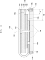
- FIG. 10 is a view illustrating an electronic device 1000 according to certain embodiments of the disclosure.
- magnetic components 1060 are disposed at the ends of the bracket to fix the electronic device 1000 in a folded state.
- the electronic device 1000 may include an electronic pen (e.g., the electronic pen 360 in FIGS. 6 and 8 ) (e.g., a stylus pen), a display 1010 (e.g., the display 200 in FIGS. 2 and 3 ), a flexible plate 1020, a digitizer 1030, a plate 1040, a bracket 1050, a magnetic component 1060, and a printed circuit board 1070.
- an electronic pen e.g., the electronic pen 360 in FIGS. 6 and 8
- a stylus pen e.g., a stylus pen
- a display 1010 e.g., the display 200 in FIGS. 2 and 3
- a flexible plate 1020 e.g., the display 200 in FIGS. 2 and 3
- a digitizer 1030 e.g., the display 200 in FIGS. 2 and 3
- a bracket 1050 e.g., a bracket 1050
- a magnetic component 1060 e.g., the magnetic component 1060,
- FIG. 10 is not drawn to scale. Certain elements are drawing larger for emphasis of certain features.
- magnetic components 1060 may be disposed on opposite sides of the bracket 1050.
- the bracket 1050 is bent at the folding area 1001, such that magnetic components are close enough to be magnetically attracted.
- a groove or hole may be formed in at least a portion of each of the opposite sides of the bracket 1050, and the magnetic components 1060 may be disposed in the grooves or holes formed on the opposite sides of the bracket 1050.
- a flexible plate 1020 may be disposed under the display 1010 to support the display 1010.
- the flexible plate 1020 may include the lattice portion 1022 so that when the electronic device 1000 is folded, the display 1010 can be smoothly supported, folded, and unfolded in the folding area 1001.
- the electronic device 1000 is folded by the lattice portion 1022 of the flexible plate 1020, operations according to folding and unfolding may be stably provided.
- the digitizer 1030 may be disposed under the flexible plate 1020.
- the plate 1040 may be disposed between the digitizer 1030 and the bracket 1050.
- the display 1010 and the digitizer 1030 may be electrically connected to the printed circuit board 1070.
- the printed circuit board 1070 may include a processor (e.g., the processor 120 in FIG. 1 ), a memory (e.g., the memory 130 in FIG. 1 ), a digitizer controller that drives the digitizer 1030, and a display driver IC that drives the display 1010.
- the digitizer 1030 may include a coil array layer 1032, a magnetic layer 1034 (e.g., a ferromagnetic sheet), and a conductive layer 1036.
- the coil array layer 1032 may include a flexible circuit board (FPCB) on which coils are disposed.
- the magnetic layer 1034 may include magnetic metal powder (MMP).
- MMP magnetic metal powder
- the conductive layer 1036 may be disposed to overlap the bracket 1050 and the magnetic component 1060.
- the display 1010 may have a thickness of about 400 ⁇ m.
- the flexible plate 1020 may have a thickness of about 170 ⁇ m.
- the coil array layer 1032 may have a thickness of about 100 ⁇ m.
- the magnetic layer 1034 (e.g., a ferromagnetic sheet) may have a thickness of about 25 ⁇ m.
- the conductive layer 1036 may have a thickness of about 12 ⁇ m.
- the plate 1040 may be disposed between the digitizer 1030 and the bracket 1050.
- the plate 1040 may be formed of a conductive metal material (e.g., aluminum, stainless steel, or a copper alloy).
- the plate 1040 may be formed of fiber reinforced plastics (FRP) or carbon fiber reinforced plastics (CFRP).
- the plate 1040 may include an opening 1040a in which at least a portion of the plate is cut.
- the opening 1040a may overlap at least a portion of the conductive layer 1036 of the digitizer 1030.
- the opening 1040a may overlap at least a portion of the bracket 1050 and at least a portion of the magnetic component 1060.
- the plate 1040 When a portion of the plate 1040 is not cut, the plate 1040 is located between the magnetic component 1060 and the conductive layer 1036 of the digitizer 1030. At least a portion of the plate 1040 is cut to form an opening 1040a, so that the magnetic component 1060 can directly affect the conductive layer 1036 of the digitizer 1030.
- the electronic pen e.g., the electronic pen 360 in FIGS. 6 and 8
- an electromagnetic induction phenomenon may occur, and the magnetic field of the electronic pen 360 (e.g., a stylus pen) may be induced into the magnetic layer 1034 of the digitizer 1030.
- the magnetic component 1060 may be located under the digitizer 1030.
- FIG. 11 is a view illustrating an electronic device 1100 according to certain embodiments of the disclosure.
- the electronic device 1100 may include an electronic pen (e.g., the electronic pen 360 in FIGS. 6 and 8 ) (e.g., a stylus pen), a display 1110 (e.g., the display 200 in FIGS. 2 and 3 ), a flexible plate 1120, a digitizer 1130, a plate 1140, a bracket 1150, a magnetic component 1160, and a printed circuit board 1170.
- an electronic pen e.g., the electronic pen 360 in FIGS. 6 and 8
- a stylus pen e.g., a stylus pen
- magnetic components 1160 may be disposed on opposite sides of the bracket 1150.
- the bracket 1150 is bent at the folding area 1101, such that magnetic components 1160 are close enough to be magnetically attracted.
- a groove or hole may be formed in at least a portion of each of the opposite sides of the bracket 1150, and the magnetic components 1160 may be disposed in the grooves or holes formed on the opposite sides of the bracket 1050.
- a flexible plate 1120 may be disposed under the display 1110 to support the display 1110.
- the flexible plate 1120 may include the lattice portion 1122 so that when the electronic device 1100 is folded, the display 1110 can be smoothly supported, folded, and unfolded in the folding area 1101.
- the electronic device 1100 is folded by the portion 1122 of the flexible plate 1120, operations according to folding and unfolding may be stably provided.
- the digitizer 1130 may be disposed under the flexible plate 1120.
- the plate 1140 may be disposed between the digitizer 1130 and the bracket 1150.
- the display 1110 and the digitizer 1130 may be electrically connected to the printed circuit board 1170.
- the printed circuit board 1170 may include a processor (e.g., the processor 120 in FIG. 1 ), a memory (e.g., the memory 130 in FIG. 1 ), a digitizer controller that drives the digitizer 1130, and a display driver IC that drives the display 1110.
- the digitizer 1130 may include a coil array layer 1132, a magnetic layer 1134 (e.g., a ferromagnetic sheet), and a conductive layer 1136.
- the coil array layer 1132 may include a flexible circuit board (FPCB) on which coils are disposed.
- the magnetic layer 1134 may include magnetic metal powder (MMP).
- the conductive layer 1136 of the digitizer 1130 may include an opening 1136a in which at least a portion of the conductive layer is cut. The opening 1136a of the conductive layer 1136 may overlap the bracket 1150 and the magnetic component 1160.
- the plate 1140 may be disposed at a level or height that is above the magnetic components 1160 and below the digitizer 1130.
- the plate 1140 may be formed of a conductive metal material (e.g., aluminum).
- the plate 1140 may include an opening 1140a in which at least a portion of the plate is cut.
- the opening 1140a of the plate 1140 may overlap at least a portion of the conductive layer 1136 of the digitizer 1130.
- the opening 1140a of the plate 1140 may overlap at least a portion of the bracket 1150 and at least a portion of the magnetic component 1160. At least a portion of the plate 1140 is cut to form the opening 1140a, so that the magnetic component 1160 may overlap the digitizer 1130.
- the opening 1136a of the conductive layer 1136 may have a first width w1
- the opening 1140a of the plate 1140 may have a second width w2 wider than the first width w1.
- the disclosure is not limited thereto, and the first width of the opening 1136a of the conductive layer 1136 and the second width of the opening 1140a of the plate 1140 may have the same size.
- the display 1110 may have a thickness of about 400 ⁇ m.
- the flexible plate 1120 may have a thickness of about 170 ⁇ m.
- the coil array layer 1132 may have a thickness of about 100 ⁇ m.
- the magnetic layer 1134 (e.g., a ferromagnetic sheet) may have a thickness of about 25 ⁇ m.
- the conductive layer 1136 may have a thickness of about 12 ⁇ m.
- the electronic pen e.g., the electronic pen 360 in FIGS. 6 and 8
- the magnetic field of the electronic pen 360 e.g., a stylus pen
- a magnetic component 1160 may be located under the digitizer 1130. Since at least a portion of the conductive layer 1136 of the digitizer 1130 is cut to form the opening 1 136a, an eddy current formed in the conductive layer 1036 of the digitizer 1030 due to a magnetic field generated by the electronic pen 360 (e.g., a stylus pen) can be reduced.
- the digitizer 1130 and the magnetic component 1160 are disposed to be spaced apart from each other by a predetermined distance, and thus it is possible to prevent or reduce the saturation of magnetic metal powder (MMP) included in the magnetic layer 1134 by the magnetic field of the magnetic component 1160. Through this, distortion of coordinates due to a nonuniform pen pressure of the electronic pen 360 (e.g., a stylus pen) or signal distortion can be prevented or reduced.
- MMP magnetic metal powder
- FIG. 12 is a view illustrating an electronic device 1200 according to certain embodiments of the disclosure.
- the electronic device 1200 may include an electronic pen (e.g., the electronic pen 360 in FIGS. 6 and 8 ) (e.g., a stylus pen), a display 1210 (e.g., the display 200 in FIGS. 2 and 3 ), a flexible plate 1220, a digitizer 1230, a plate 1240, a bracket 1250, a magnetic component 1260, and a printed circuit board 1270.
- an electronic pen e.g., the electronic pen 360 in FIGS. 6 and 8
- a stylus pen e.g., a stylus pen
- a display 1210 e.g., the display 200 in FIGS. 2 and 3
- a flexible plate 1220 e.g., the display 200 in FIGS. 2 and 3
- a digitizer 1230 e.g., the display 200 in FIGS. 2 and 3
- a bracket 1250 e.g., a bracket 1250
- a magnetic component 1260 e.g., a magnetic component 12
- magnetic components 1260 may be disposed on opposite sides of the bracket 1250.
- the bracket 1250 is bent at the folding area 1201, such that magnetic components 1260 are close enough to be magnetically attracted.
- a groove or hole may be formed in at least a portion of each of the opposite sides of the bracket 1250, and the magnetic components 1260 may be disposed in the grooves or holes formed on the opposite sides of the bracket 1250.
- a flexible plate 1220 may be disposed under the display 1210 to support the display 1210.
- the flexible plate 1220 may include the lattice portion 1222 so that when the electronic device 1200 is folded, the display 1210 can be smoothly supported, folded, and unfolded in the folding area 1201.
- the electronic device 1200 is folded by the lattice portion 1222 of the flexible plate 1220, operations according to folding and unfolding may be stably provided.
- the digitizer 1230 may be disposed under the flexible plate 1220.
- the plate 1240 may be disposed between the digitizer 1230 and the bracket 1250.
- the display 1210 and the digitizer 1230 may be electrically connected to the printed circuit board 1270.
- the printed circuit board 1270 may include a processor (e.g., the processor 120 in FIG. 1 ), a memory (e.g., the memory 130 in FIG. 1 ), a digitizer controller that drives the digitizer 1230, and a display driver IC that drives the display 1210.
- the digitizer 1230 may include a coil array layer 1232, a magnetic layer 1234 (e.g., a ferromagnetic sheet), a conductive layer 1236, and a magnetic shield layer 1238.
- the coil array layer 1232 may include a flexible circuit board (FPCB) on which coils are disposed.
- the magnetic layer 1234 may include magnetic metal powder (MMP).
- MMP magnetic metal powder
- the conductive layer 1236 of the digitizer 1230 may include an opening 1236a in which at least a portion of the conductive layer is cut.
- the magnetic shield layer 1238 may be disposed in the opening 1236a of the conductive layer 1236.
- the magnetic shield layer 1238 may also be disposed above the printed circuit board 1270.
- the magnetic shield layer 1238 may include amorphous silicon, steel plate cold commercial (SPCC), and/or permalloy.
- the magnetic shield layer 1238 may overlap the bracket 1250 and the magnetic component 1260.
- the display 1210 may have a thickness of about 400 ⁇ m.
- the flexible plate 1220 may have a thickness of about 170 ⁇ m.
- the coil array layer 1232 may have a thickness of about 100 ⁇ m.
- the magnetic layer 1234 (e.g., a ferromagnetic sheet) may have a thickness of about 25 ⁇ m.
- the conductive layer 1236 may have a thickness of about 12 ⁇ m.
- the magnetic shield layer 1238 may have a thickness of about 200 ⁇ m.
- the plate 1240 may be disposed at a level or height that is above the magnetic components 1260 and below the digitizer 1230.
- the plate 1240 may be formed of a conductive metal material (e.g., aluminum).
- the plate 1240 may include an opening 1240a in which at least a portion of the plate is cut.
- the opening 1240a of the plate 1240 may overlap at least a portion of the conductive layer 1236 of the digitizer 1230 and the magnetic shield layer 1238.
- the opening 1240a of the plate 1240 may overlap at least a portion of the bracket 1250 and at least a portion of the magnetic component 1260. At least a portion of the plate 1240 is cut to form the opening 1240a, so that the magnetic component 1260 may overlap the digitizer 1230.
- the opening 1236a of the conductive layer 1236 may have a first width w1
- the opening 1240a of the plate 1240 may have a second width w2 wider than the first width w1.
- the electronic pen e.g., the electronic pen 360 in FIGS. 6 and 8
- the electronic pen e.g., the electronic pen 360 in FIGS. 6 and 8
- an electromagnetic induction phenomenon may occur, and the magnetic field of the electronic pen 360 (e.g., a stylus pen) may be induced into the magnetic layer 1234 of the digitizer 1230.
- the magnetic component 1260 may be located under the digitizer 1230.
- the conductive layer 1236 of the digitizer 1230 may be cut to form an opening, and the magnetic shield layer 1238 is disposed in the opening, it is possible to reduce the eddy current formed in the conductive layer 1236 of the digitizer 1230 due to the magnetic field generated from the electronic pen 360 (e.g., a stylus pen). Through this, distortion of coordinates due to a nonuniform pen pressure of the electronic pen 360 (e.g., a stylus pen) or signal distortion can be prevented or reduced.
- FIG. 13 is a view illustrating an electronic device according to certain embodiments of the disclosure.
- the electronic device 1300 may include an electronic pen (e.g., the electronic pen 360 in FIGS. 6 and 8 ) (e.g., a stylus pen), a display 1310 (e.g., the display 200 in FIGS. 2 and 3 ), a flexible plate 1320, a digitizer 1330, a plate 1340, a bracket 1350, a magnetic component 1360, and a printed circuit board 1370.
- an electronic pen e.g., the electronic pen 360 in FIGS. 6 and 8
- a stylus pen e.g., a stylus pen
- a display 1310 e.g., the display 200 in FIGS. 2 and 3
- a flexible plate 1320 e.g., the display 200 in FIGS. 2 and 3
- a digitizer 1330 e.g., the display 200 in FIGS. 2 and 3
- a bracket 1350 e.g., a bracket 1350
- a magnetic component 1360 e.g., a magnetic component 13
- magnetic components 1360 may be disposed on opposite sides of the bracket 1350.
- the bracket 1350 is bent at the folding area 1301, such that magnetic components 1360 are close enough to be magnetically attracted.
- a groove or hole may be formed in at least a portion of each of the opposite sides of the bracket 1350, and the magnetic components 1360 may be disposed in the grooves or holes formed on the opposite sides of the bracket 1050.
- a flexible plate 1320 may be disposed under the display 1310 to support the display 1310.
- the flexible plate 1320 may include the lattice portion 1322 so that when the electronic device 1300 is folded, the display 1310 can be smoothly supported, folded, and unfolded in the folding area 1301.
- the electronic device 1300 is folded by the lattice portion 1322 of the flexible plate 1320, operations according to folding and unfolding may be stably provided.
- the digitizer 1330 may be disposed under the flexible plate 1320.
- the plate 1340 may be disposed between the digitizer 1330 and the bracket 1350.
- the display 1310 and the digitizer 1330 may be electrically connected to the printed circuit board 1370.
- the printed circuit board 1370 may include a processor (e.g., the processor 120 in FIG. 1 ), a memory (e.g., the memory 130 in FIG. 1 ), a digitizer controller that drives the digitizer 1330, and a display driver IC that drives the display 1310.
- the digitizer 1330 may include a coil array layer 1332, a magnetic layer 1334 (e.g., a ferromagnetic sheet), a conductive layer 1336, and a magnetic shield layer 1338.
- the coil array layer 1332 may include a flexible circuit board (FPCB) on which coils are disposed.
- the magnetic layer 1334 may include magnetic metal powder (MMP).
- MMP magnetic metal powder
- the conductive layer 1336 of the digitizer 1330 may include an opening 1336a in which at least a portion of the conductive layer is cut.
- the magnetic shield layer 1338 may be disposed in the opening 1336a of the conductive layer 1336.
- the magnetic shield layer 1338 may also be disposed above the printed circuit board 1370.
- the magnetic shield layer 1338 may include amorphous silicon, steel plate cold commercial (SPCC), and/or permalloy.
- the magnetic shield layer 1338 may overlap the bracket 1350 and the magnetic component 1360.
- the magnetic shield layer 1338 is spaced apart from the end 1336b of the magnetic layer 1334 by a predetermined distance d1 so that the magnetic shield layer 1338 may overlap a portion of the magnetic component 1360.
- the plate 1340 may be disposed at a level or height that is above the magnetic components 1360 and below the digitizer 1330.
- the plate 1340 may be formed of a conductive metal material (e.g., aluminum).
- the plate 1340 may include an opening 1340a in which at least a portion of the plate is cut.
- the opening 1340a of the plate 1340 may overlap at least a portion of the conductive layer 1336 of the digitizer 1330 and the magnetic shield layer 1338.
- the opening 1340a of the plate 1340 may overlap at least a portion of the bracket 1350 and at least a portion of the magnetic component 1360. At least a portion of the plate 1340 is cut to form the opening 1340a, so that the magnetic component 1360 may overlap the digitizer 1330.
- the electronic pen e.g., the electronic pen 360 in FIGS. 6 and 8
- an electromagnetic induction phenomenon may occur, and the magnetic field of the electronic pen 360 (e.g., a stylus pen) may be induced into the magnetic layer 1334 of the digitizer 1330.
- the magnetic component 1360 may be located under the digitizer 1330. At least a portion of the conductive layer 1336 of the digitizer 1330 may be cut to form an opening 1336a, and a magnetic shield layer 1338 may be disposed in the opening 1336a so that the saturation 1334a of the magnetic layer 1334 can be reduced.
- an eddy current formed in the conductive layer 1336 of the digitizer 1330 due to a magnetic field generated by the electronic pen 360 can be reduced.
- distortion of coordinates due to a nonuniform pen pressure of the electronic pen 360 (e.g., a stylus pen) or signal distortion can be prevented or reduced.
- FIG. 14 is a view illustrating an electronic device 1400 according to certain embodiments of the disclosure.
- the electronic device 1400 may include an electronic pen (e.g., the electronic pen 360 in FIGS. 6 and 8 ) (e.g., a stylus pen), a display 1410 (e.g., the display 200 in FIGS. 2 and 3 ), a flexible plate 1420, a digitizer 1430, a bracket 1450, a magnetic component 1460, a printed circuit board 1470, and a magnetic shield part 1480.
- an electronic pen e.g., the electronic pen 360 in FIGS. 6 and 8
- a stylus pen e.g., a stylus pen
- a display 1410 e.g., the display 200 in FIGS. 2 and 3
- a digitizer 1430 e.g., the display 200 in FIGS. 2 and 3
- a bracket 1450 e.g., the bracket 1450
- a magnetic component 1460 e.g., the magnetic component 1460
- printed circuit board 1470 e.g., a printed circuit board 1470
- magnetic components 1460 may be disposed on opposite sides of the bracket 1450.
- the bracket 1450 is bent at the folding area 1401, such that magnetic components 1460 are close enough to be magnetically attracted.
- a groove or hole may be formed in at least a portion of each of the opposite sides of the bracket 1450, and the magnetic components 1460 may be disposed in the grooves or holes formed on the opposite sides of the bracket 1450.
- a flexible plate 1420 may be disposed under the display 1410 to support the display 1410.
- the flexible plate 1420 may include the lattice portion 1422 so that when the electronic device 1400 is folded, the display 1410 can be smoothly supported, folded, and unfolded in the folding area 1401.
- the electronic device 1400 is folded by the lattice portion 1422 of the flexible plate 1420, operations according to folding and unfolding may be stably provided.
- the digitizer 1430 may be disposed under the flexible plate 1420.
- the magnetic shield part 1480 may be disposed between the digitizer 1430 and the bracket 1450.
- the display 1410 and the digitizer 1430 may be electrically connected to the printed circuit board 1470.
- the printed circuit board 1470 may include a processor (e.g., the processor 120 in FIG. 1 ), a memory (e.g., the memory 130 in FIG. 1 ), a digitizer controller that drives the digitizer 1430, and a display driver IC that drives the display 1410.
- the digitizer 1430 may include a coil array layer 1432, a magnetic layer 1434 (e.g., a ferromagnetic sheet), and a conductive layer 1436.
- the coil array layer 1432 may include a flexible circuit board (FPCB) on which coils are disposed.
- the magnetic layer 1434 may include magnetic metal powder (MMP).
- the conductive layer 1436 of the digitizer 1430 may include slits 1438 in which at least a portion of the conductive layer is cut. The slits 1438 may be formed to at least partially overlap the magnetic shield part 1480.
- the magnetic shield part 1480 may be disposed to overlap the entire upper end of the magnetic component 1460.
- the magnetic shield layer 1480 may also be disposed under the printed circuit board 1470.
- the magnetic shield part 1480 may include amorphous silicon, steel plate cold commercial (SPCC), and/or permalloy.
- the electronic pen e.g., the electronic pen 360 in FIGS. 6 and 8
- an electromagnetic induction phenomenon may occur, and the magnetic field of the electronic pen 360 (e.g., a stylus pen) may be induced into the magnetic layer 1434 of the digitizer 1430.
- the magnetic component 1460 may be located under the digitizer 1430. At least a portion of the conductive layer 1436 of the digitizer 1430 may be cut to form slits 1438, thereby reducing saturation of the magnetic layer 1434.
- the magnetic shield part 1480 is disposed to overlap the magnetic component 1460, an eddy current formed in the conductive layer 1436 of the digitizer 1430 due to a magnetic field generated by the electronic pen 360 (e.g., a stylus pen) can be reduced. Through this, distortion of coordinates due to a nonuniform pen pressure of the electronic pen 360 (e.g., a stylus pen) or signal distortion can be prevented or reduced.
- FIG. 15 is a view illustrating an electronic device 1500 according to certain embodiments of the disclosure.
- the electronic device 1500 may include an electronic pen (e.g., the electronic pen 360 in FIGS. 6 and 8 ) (e.g., a stylus pen), a display 1510 (e.g., the display 200 in FIGS. 2 and 3 ), a flexible plate 1520, a digitizer 1530, a bracket 1550, a magnetic component 1560, a printed circuit board 1570, and a magnetic shield part 1580.
- an electronic pen e.g., the electronic pen 360 in FIGS. 6 and 8
- a stylus pen e.g., a stylus pen
- magnetic components 1560 may be disposed on opposite sides of the bracket 1550.
- a groove or hole may be formed in at least a portion of each of the opposite sides of the bracket 1550, and the magnetic components 1560 may be disposed in the grooves or holes formed on the opposite sides of the bracket 1550.
- a flexible plate 1520 may be disposed under the display 1510 to support the display 1510.
- the flexible plate 1520 may include the lattice portion 1522 so that when the electronic device 1500 is folded, the display 1510 can be smoothly supported, folded, and unfolded in the folding area 1501.
- the electronic device 1500 is folded by the lattice portion 1522 of the flexible plate 1520, operations according to folding and unfolding may be stably provided.
- the digitizer 1530 may be disposed under the flexible plate 1520.
- the magnetic shield part 1580 may be disposed between the digitizer 1530 and the bracket 1550.
- the display 1510 and the digitizer 1530 may be electrically connected to the printed circuit board 1570.
- the printed circuit board 1570 may include a processor (e.g., the processor 120 in FIG. 1 ), a memory (e.g., the memory 130 in FIG. 1 ), a digitizer controller that drives the digitizer 1530, and a display driver IC that drives the display 1510.
- the digitizer 1530 may include a coil array layer 1532, a magnetic layer 1534 (e.g., a ferromagnetic sheet), and a conductive layer 1536.
- the coil array layer 1532 may include a flexible circuit board (FPCB) on which coils are disposed.
- the magnetic layer 1534 may include magnetic metal powder (MMP).
- the conductive layer 1536 of the digitizer 1530 may include slits 1538 in which at least a portion of the conductive layer is cut. The slits 1538 may be formed to at least partially overlap the magnetic shield part 1580 and the magnetic component 1560.
- the magnetic shield part 1580 is disposed to be spaced apart from an end of the magnetic layer 1534 by a predetermined distance d1 so that the magnetic shield part 1580 can be disposed to overlap a portion of the upper end of the magnetic component 1560.
- the magnetic shield layer 1580 may also be disposed under the printed circuit board 1570.
- the magnetic shield part 1580 may include amorphous silicon, steel plate cold commercial (SPCC), and/or permalloy.
- the electronic pen e.g., the electronic pen 360 in FIGS. 6 and 8
- an electromagnetic induction phenomenon may occur, and the magnetic field of the electronic pen 360 (e.g., a stylus pen) may be induced into the magnetic layer 1534 of the digitizer 1530.
- the magnetic component 1560 may be located under the digitizer 1530. At least a portion of the conductive layer 1536 of the digitizer 1530 may be cut to form slits 1538, thereby reducing saturation of the magnetic layer 1534.
- the magnetic shield part 1580 is disposed to at least partially overlap the magnetic component 1560, an eddy current formed in the conductive layer 1536 of the digitizer 1530 due to a magnetic field generated by the electronic pen 360 (e.g., a stylus pen) can be reduced. Through this, distortion of coordinates due to a nonuniform pen pressure of the electronic pen 360 (e.g., a stylus pen) or signal distortion can be prevented or reduced.
- FIG. 16 is a view illustrating an electronic device 1600 according to certain embodiments of the disclosure.
- the electronic device 1600 may include an electronic pen (e.g., the electronic pen 360 in FIGS. 6 and 8 ) (e.g., a stylus pen), a display 1610 (e.g., the display 200 in FIGS. 2 and 3 ), a flexible plate 1620, a digitizer 1630, a bracket 1650, a magnetic component 1660, a printed circuit board 1670, and a magnetic shield part 1680.
- an electronic pen e.g., the electronic pen 360 in FIGS. 6 and 8
- a stylus pen e.g., a stylus pen
- magnetic components 1660 may be disposed on opposite sides of the bracket 1650.
- a groove or hole may be formed in at least a portion of each of the opposite sides of the bracket 1650, and the magnetic components 1660 may be disposed in the grooves or holes formed on the opposite sides of the bracket 1650.
- a flexible plate 1620 may be disposed under the display 1610 to support the display 1610.
- the flexible plate 1620 may include the lattice portion 1622 so that when the electronic device 1600 is folded, the display 1610 can be smoothly supported, folded, and unfolded in the folding area 1601.
- the electronic device 1600 is folded by the lattice portion 1622 of the flexible plate 1620, operations according to folding and unfolding may be stably provided.
- the digitizer 1630 may be disposed under the flexible plate 1620.
- the magnetic shield part 1680 may be disposed between the digitizer 1630 and the bracket 1650.
- the display 1610 and the digitizer 1630 may be electrically connected to the printed circuit board 1670.
- the printed circuit board 1670 may include a processor (e.g., the processor 120 in FIG. 1 ), a memory (e.g., the memory 130 in FIG. 1 ), a digitizer controller that drives the digitizer 1630, and a display driver IC that drives the display 1610.
- the digitizer 1630 may include a coil array layer 1632, a magnetic layer 1634 (e.g., a ferromagnetic sheet), and a conductive layer 1636.
- the coil array layer 1632 may include a flexible circuit board (FPCB) on which coils are disposed.
- the magnetic layer 1634 may include magnetic metal powder (MMP).
- the conductive layer 1636 of the digitizer 1630 may include an opening 1636a in which a portion of the conductive layer is cut. The opening 1636a of the conductive layer 1636 may be formed to at least partially overlap the magnetic shield part 1680 and the magnetic component 1660.
- the magnetic shield part 1680 may be disposed to surround the side surface 1662 and the bottom surface 1664 of the magnetic component 1660.
- the magnetic shield part 1680 may be disposed to cover at least a portion of the top surface 1652 of the bracket 1650.
- the magnetic shield part 1680 may also be disposed on a portion overlapping the printed circuit board 1670.
- the magnetic shield part 1680 may include amorphous silicon, steel plate cold commercial (SPCC), and/or permalloy.
- the electronic pen e.g., the electronic pen 360 in FIGS. 6 and 8
- an electromagnetic induction phenomenon may occur, and the magnetic field of the electronic pen 360 (e.g., a stylus pen) may be induced into the magnetic layer 1634 of the digitizer 1630.
- the magnetic component 1660 may be located under the digitizer 1630. At least a portion of the conductive layer 1636 of the digitizer 1630 may be cut to form an opening 1636a. Since the opening 1636a is formed in at least a portion of the conductive layer 1636, saturation of the magnetic layer 1634 can be reduced.
- the magnetic shield part 1680 is around the magnetic component 1660, an eddy current formed in the conductive layer 1636 of the digitizer 1630 due to a magnetic field generated by the electronic pen 360 (e.g., a stylus pen) can be reduced. Through this, distortion of coordinates due to a nonuniform pen pressure of the electronic pen 360 (e.g., a stylus pen) or signal distortion can be prevented or reduced.
- FIG. 17 is a view illustrating an electronic device 1700 according to certain embodiments of the disclosure.
- the electronic device 1700 may include an electronic pen (e.g., the electronic pen 360 in FIGS. 6 and 8 ) (e.g., a stylus pen), a display 1710 (e.g., the display 200 in FIGS. 2 and 3 ), a flexible plate 1720, a digitizer 1705, a bracket 1750, a magnetic component 1760, a printed circuit board 1770, a plate 1780, and a magnetic shield part 1790.
- an electronic pen e.g., the electronic pen 360 in FIGS. 6 and 8
- a stylus pen e.g., a stylus pen
- a display 1710 e.g., the display 200 in FIGS. 2 and 3
- a digitizer 1705 e.g., the display 200 in FIGS. 2 and 3
- a bracket 1750 e.g., the bracket 1750
- a magnetic component 1760 e.g., a printed circuit board 1770
- plate 1780 e.g., a plate 17
- magnetic components 1760 may be disposed on opposite sides of the bracket 1750.
- a groove or hole may be formed in at least a portion of each of the opposite sides of the bracket 1750, and the magnetic components 1760 may be disposed in the grooves or holes formed on the opposite sides of the bracket 1750.
- a flexible plate 1720 may be disposed under the display 1710 to support the display 1710.
- the flexible plate 1720 may include the lattice portion 1722 so that when the electronic device 1700 is folded, the display 1710 can be smoothly supported, folded, and unfolded in the folding area 1701.
- the electronic device 1700 is folded by the lattice portion 1722 of the flexible plate 1720, operations according to folding and unfolding may be stably provided.
- the digitizer 1705 may be disposed under the flexible plate 1720.
- the digitizer 1705 may include a coil array layer 1730, a magnetic plate 1740 (e.g., magnetic metal powder (MMP)), and a plate 1780.
- the magnetic plate 1740 may be disposed under the coil array layer 1730.
- the plate 1780 may be disposed under the magnetic plate 1740.
- the magnetic shield part 1790 may be disposed under the plate 1780.
- the digitizer 1705 may be configured to include the magnetic shield part 1790.
- the display 1710 and the digitizer 1705 may be electrically connected to the printed circuit board 1770.
- the printed circuit board 1770 may include a processor (e.g., the processor 120 in FIG. 1 ), a memory (e.g., the memory 130 in FIG. 1 ), a digitizer controller that drives the digitizer 1705, and a display driver IC that drives the display 1710.
- the plate 1780 may include an opening 1780a in which at least a portion of the plate is cut.
- the opening 1780a of the plate 1780 may overlap the magnetic component 1760.
- the magnetic shield part 1790 may be disposed between the plate 1780 and the magnetic component 1760.
- the electronic pen e.g., the electronic pen 360 in FIGS. 6 and 8
- the magnetic field of the electronic pen 360 e.g., a stylus pen
- the magnetic shield part 1790 By disposing the magnetic shield part 1790 on the entire bottom surface of the digitizer 1705 and forming an opening 1780a of the plate 1780 in a portion overlapping the magnetic component 1760, the influence of the magnetic field of the magnetic component 1760 on the digitizer 1705 can be reduced.
- an eddy current formed in the digitizer 1705 due to a magnetic field generated by the electronic pen 360 e.g., a stylus pen
- saturation of the magnetic plate 1740 e.g., magnetic metal powder (MMP)
- MMP magnetic metal powder
- FIG. 18 is a view illustrating an electronic device 1800 according to certain embodiments of the disclosure.
- the electronic device 1800 may include an electronic pen (e.g., the electronic pen 360 in FIGS. 6 and 8 ) (e.g., a stylus pen), a display 1810 (e.g., the display 200 in FIGS. 2 and 3 ), a flexible plate 1820, a digitizer 1805, a bracket 1850, a magnetic component 1860, and a printed circuit board 1870.
- the digitizer 1805 may include a coil array layer 1830, a magnetic plate 1840 (e.g., magnetic metal powder (MMP)), a plate 1880 (e.g., a conductive plate), and a magnetic shield part 1890.
- MMP magnetic metal powder
- magnetic components 1860 may be disposed on opposite sides of the bracket 1850.
- a groove or hole may be formed in at least a portion of each of the opposite sides of the bracket 1850, and the magnetic components 1860 may be disposed in the grooves or holes formed on the opposite sides of the bracket 1850.
- a flexible plate 1820 may be disposed under the display 1810 to support the display 1810.
- the flexible plate 1820 may include the lattice portion 1822 so that when the electronic device 1800 is folded, the display 1810 can be smoothly supported, folded, and unfolded in the folding area 1801.
- the electronic device 1800 is folded by the lattice portion 1822 of the flexible plate 1820, operations according to folding and unfolding may be stably provided.
- the digitizer 1805 may be disposed under the flexible plate 1820.
- the magnetic plate 1840 may be disposed under the digitizer 1805.
- the magnetic shield part 1890 may be disposed under the magnetic plate 1840.
- the plate 1880 may be disposed under the magnetic shield part 1890.
- the display 1810 and the digitizer 1805 may be electrically connected to the printed circuit board 1870.
- the printed circuit board 1870 may include a processor (e.g., the processor 120 in FIG. 1 ), a memory (e.g., the memory 130 in FIG. 1 ), a digitizer controller that drives the digitizer 1805, and a display driver IC that drives the display 1810.
- the magnetic shield part 1890 may be disposed between the magnetic plate 1840 and the plate 1780.
- the magnetic shield part 1890 may overlap the digitizer 1805 and the plate 1880.
- the plate 1880 may be disposed between the magnetic shield part 1890 and the bracket 1850.
- the plate 1880 may overlap the magnetic shield part 1890 and the magnetic component 1860.
- the electronic pen e.g., the electronic pen 360 in FIGS. 6 and 8
- the electronic pen e.g., the electronic pen 360 in FIGS. 6 and 8
- an electromagnetic induction phenomenon may occur, and the magnetic field of the electronic pen 360 (e.g., a stylus pen) may be induced into the digitizer 1805.
- the magnetic shield part 1890 By disposing the magnetic shield part 1890 on the entire bottom surface of the digitizer 1805 and disposing the plate 1880 on the entire bottom surface of the magnetic shield part 1890, the influence of the magnetic field of the magnetic component 1860 on the digitizer 1805 can be reduced.
- an eddy current formed in the digitizer 1805 due to a magnetic field generated by the electronic pen 360 e.g., a stylus pen
- saturation of the magnetic plate 1840 e.g., magnetic metal powder (MMP)
- MMP magnetic metal powder
- FIG. 19 is a view illustrating a bracket (e.g., an aluminum bracket) disposed to surround a magnetic component.
- a bracket e.g., an aluminum bracket
- a bracket 1910 of an electronic device 1900 may be formed of a metal material such as aluminum, and a display module (e.g., the display module 160 in FIG. 1 ) may be attached to the bracket 1910.
- a groove or hole 1912 may be formed in a portion of the bracket 1910, and a magnetic component 1920 may be disposed in the groove or hole 1912 of the bracket 1910.
- an eddy current 1930 may be generated.
- FIG. 20 is a view illustrating a bracket (e.g., an aluminum bracket) disposed to surround a magnetic component according to certain embodiments of the disclosure.
- the bracket 2010 includes a slit 2014 to reduce eddy currents.
- a groove or hole 2012 may be formed in the bracket 2010 of the electronic device 2000, and a magnetic component 2020 may be disposed in the groove or hole 2012 of the bracket 2010.
- a slit 2014 may be formed in at least a portion of the bracket 2010 so that a closed loop is not formed in the bracket 2010.
- the slit 2014 may be formed in a portion adjacent to the magnetic component 2020 in the entire area of the bracket 2010.
- the slit 2014 may be formed in a portion adjacent to one side surface of the magnetic component 2020.
- the disclosure is not limited thereto, and a plurality of slits may be formed in portions adjacent to a plurality of side surfaces of the magnetic component 2020.
- An electronic device (e.g., the electronic device 101 in FIGS. 2 and 3 , the electronic device 1000 in FIG. 10 , the electronic device 1100 in FIG. 11 , the electronic device 1200 in FIG. 12 , the electronic device 1300 in FIG. 13 , the electronic device 1400 in FIG. 14 , the electronic device 1500 in FIG. 15 , the electronic device 1600 in FIG. 16 , the electronic device 1700 in FIG. 17 , the electronic device 1800 in FIG. 18 , the electronic device 1900 in FIG. 19 , or the electronic device 2000 of FIG. 20 ) according to certain embodiments of the disclosure may include a display (e.g., the display 200 in FIGS. 2 and 3 , the display 1010 in FIG. 10 , the display 1110 in FIG.
- a display e.g., the display 200 in FIGS. 2 and 3 , the display 1010 in FIG. 10 , the display 1110 in FIG.
- a coil array layer e.g., the coil array layer 410 in FIG. 4 , the coil array 610 in FIG. 6 , the coil array layer 810 in FIG. 8 , the coil array layer 1032 in FIG. 10 , the coil array layer 1132 in FIG. 11 , the coil array layer 1232 in FIG. 12 , the coil array 1332 in FIG. 13 , the coil array layer 1432 in FIG. 14 , the coil array layer 1532 in FIG.
- a magnetic layer e.g., the magnetic layer 420 in FIG. 4 , the magnetic layer 620 in FIG. 6 , the magnetic layer 820 in FIG. 8 , the magnetic layer 1034 in FIG. 10 , the magnetic layer 1134 in FIG. 11 , the magnetic layer 1234 in FIG. 12 , the magnetic layer 1334 in FIG. 13 , the magnetic layer 1434 in FIG. 14 , the magnetic layer 1534 in FIG. 15 , or the magnetic layer 1634 in FIG.
- a magnetic layer e.g., the magnetic layer 420 in FIG. 4 , the magnetic layer 620 in FIG. 6 , the magnetic layer 820 in FIG. 8 , the magnetic layer 1034 in FIG. 10 , the magnetic layer 1134 in FIG. 11 , the magnetic layer 1234 in FIG. 12 , the magnetic layer 1334 in FIG. 13 , the magnetic layer 1434 in FIG. 14 , the magnetic layer 1534 in FIG. 15 , or the magnetic layer 1634 in FIG.
- a conductive layer e.g., the conductive layer 430 in FIG. 4 , the conductive layer 630 in FIG. 6 , the conductive layer 830 in FIG. 8 , and the conductive layer 1036 in FIG. 10 , the conductive layer 1136 in FIG. 11 , the conductive layer 1236 in FIG. 12 , the conductive layer 1336 in FIG. 13 , the conductive layer 1436 in FIG. 14 , conductive layer 1536 in FIG. 15 , or the conductive layer 1636 in FIG.
- a conductive layer e.g., the conductive layer 430 in FIG. 4 , the conductive layer 630 in FIG. 6 , the conductive layer 830 in FIG. 8 , and the conductive layer 1036 in FIG. 10 , the conductive layer 1136 in FIG. 11 , the conductive layer 1236 in FIG. 12 , the conductive layer 1336 in FIG. 13 , the conductive layer 1436 in FIG. 14 , conductive layer 1536 in FIG. 15 , or the conductive
- a conductive plate e.g., the plate 640 in FIG. 6 , the plate 840 in FIG. 8 , the plate 1040 in FIG. 10 , the plate 1140 in FIG. 11 , the plate 1240 in FIG. 12 , the plate 1340 in FIG. 13 , the plate 1780 in FIG. 17 , or the plate 1880 in FIG. 18 ) disposed under the conductive layer, a bracket (e.g., the bracket 1050 in FIG. 10 , the bracket 1150 in FIG. 11 , the bracket 1250 in FIG. 12 , the bracket 1350 in FIG.
- a bracket e.g., the bracket 1050 in FIG. 10 , the bracket 1150 in FIG. 11 , the bracket 1250 in FIG. 12 , the bracket 1350 in FIG.
- the bracket 1450 in FIG. 14 the bracket 1550 in FIG. 15 , the bracket 1650 in FIG. 16 , the bracket 1750 of FIG. 17 , the bracket 1850 in FIG. 18 , the bracket 1910 in FIG. 19 , or the bracket 2010 of FIG. 20 ), and a magnetic component (e.g., the magnetic component 440 in FIG. 4 , the magnetic component 650 in FIG. 6 , the magnetic component 850 in FIG. 8 , the magnetic component 1060 in FIG. 10 , the magnetic component 1160 in FIG. 11 , the magnetic component 1260 in FIG. 12 , the magnetic component 1360 in FIG. 13 , the magnetic component 1460 in FIG. 14 , the magnetic component 1560 in FIG. 15 , the magnetic component 1660 in FIG.
- a magnetic component e.g., the magnetic component 440 in FIG. 4 , the magnetic component 650 in FIG. 6 , the magnetic component 850 in FIG. 8 , the magnetic component 1060 in FIG. 10 , the magnetic component 1160 in FIG. 11 , the magnetic
- the conductive plate 640, 840, 1040, 1140, 1240, 1340, 1780, or 1880 may be disposed under the digitizer 400, 600, 800, 1030, 1130, 1230, 1330, 1430, 1530, 1630, 1705, or 1805.
- the bracket 1050, 1150, 1250, 1350, 1450, 1550, 1650, 1750, 1850, 1910, or 2010 may be disposed under the conductive plate 640, 840, 1040, 1140, 1240, 1340, 1780, or 1880.
- the magnetic component 440, 650, 850, 1060, 1160, 1260, 1360, 1460, 1560, 1660, 1760, 1860, 1920, or 2020 may be disposed under the bracket 1050, 1150, 1250, 1350, 1450, 1550, 1650, 1750, 1850, 1910, or 2010.
- the digitizer 400, 600, 800, 1030, 1130, 1230, 1330, 1430, 1530, 1630, 1705, or 1805 may include wherein the conductive layer 430, 630, 830, 1036, 1136, 1236, 1336, 1436, 1536, or 1636 has a first opening, and the first opening and the magnetic component 440, 650, 850, 1060, 1160, 1260, 1360, 1460, 1560, 1660, 1760, 1860, 1920, or 2020 may at least partially overlap each other.
- At least a portion of the conductive plates 640, 840, 1040, 1140, 1240, 1340, 1780, or 1880 may have a second opening.
- the second opening and the magnetic components 440, 650, 850, 1060, 1160, 1260, 1360, 1460, 1560, 1660, 1760, 1860, 1920, or 2020 at least partially overlap each other.
- the first opening may have a first width.
- the second opening may have a second width wider than the first width.
- the electronic device 101, 1000, 1100, 1200, 1300, 1400, 1500, 1600, 1700, 1800, 1900, or 2000 may further include a magnetic shield layer disposed in the first opening.
- the magnetic shield layer may include amorphous silicon, steel plate cold commercial (SPCC), or permalloy.
- the magnetic shield layer may overlap the entire top surface of the magnetic component 440, 650, 850, 1060, 1160, 1260, 1360, 1460, 1560, 1660, 1760, 1860, 1920, or 2020.
- the magnetic shield layer may be spaced apart from an end of the magnetic layer 420, 620, 820, 1034, 1134, 1234, 1334, 1434, 1534, or 1634 by a predetermined distance, and may overlap a portion of the top surface of the magnetic component 440, 650, 850, 1060, 1160, 1260, 1360, 1460, 1560, 1660, 1760, 1860, 1920, or 2020.
- the magnetic component 440, 650, 850, 1060, 1160, 1260, 1360, 1460, 1560, 1660, 1760, 1860, 1920, or 2020 may be disposed in a groove or hole formed in the bracket 1050, 1150, 1250, 1350, 1450, 1550, 1650, 1750, 1850, 1910, or 2010).
- a slit may be formed in at least a portion of the bracket 1050, 1150, 1250, 1350, 1450, 1550, 1650, 1750, 1850, 1910, or 2010 located adjacent to the magnetic component 440, 650, 850, 1060, 1160, 1260, 1360, 1460, 1560, 1660, 1760, 1860, 1920, or 2020.
- An electronic device (e.g., the electronic device 101 in FIGS. 2 and 3 , the electronic device 1000 in FIG. 10 , the electronic device 1100 in FIG. 11 , the electronic device 1200 in FIG. 12 , the electronic device 1300 in FIG. 13 , the electronic device 1400 in FIG. 14 , the electronic device 1500 in FIG. 15 , the electronic device 1600 in FIG. 16 , the electronic device 1700 in FIG. 17 , the electronic device 1800 in FIG. 18 , the electronic device 1900 in FIG. 19 , or the electronic device 2000 of FIG. 20 ) according to certain embodiments of the disclosure may include a display (e.g., the display 200 in FIGS. 2 and 3 , the display 1010 in FIG. 10 , the display 1110 in FIG.
- a display e.g., the display 200 in FIGS. 2 and 3 , the display 1010 in FIG. 10 , the display 1110 in FIG.
- a coil array layer e.g., the coil array layer 410 in FIG. 4 , the coil array 610 in FIG. 6 , the coil array layer 810 in FIG. 8 , the coil array layer 1032 in FIG. 10 , the coil array layer 1132 in FIG. 11 , the coil array layer 1232 in FIG. 12 , the coil array 1332 in FIG. 13 , the coil array layer 1432 in FIG. 14 , the coil array layer 1532 in FIG.
- the coil array layer 1632 in FIG. 16 the coil array layer 1730 in FIG. 17 , or the coil array 1830 in FIG. 18
- a magnetic layer e.g., the magnetic layer 420 in FIG. 4 , the magnetic layer 620 in FIG. 6 , the magnetic layer 820 in FIG. 8 , the magnetic layer 1034 in FIG. 10 , the magnetic layer 1134 in FIG. 11 , the magnetic layer 1234 in FIG. 12 , the magnetic layer 1334 in FIG. 13 , the magnetic layer 1434 in FIG. 14 , the magnetic layer 1534 in FIG. 15 , or the magnetic layer 1634 in FIG.
- a conductive layer e.g., the conductive layer 430 in FIG. 4 , the conductive layer 630 in FIG. 6 , the conductive layer 830 in FIG. 8 , and the conductive layer 1036 in FIG. 10 , the conductive layer 1136 in FIG. 11 , the conductive layer 1236 in FIG. 12 , the conductive layer 1336 in FIG. 13 , the conductive layer 1436 in FIG. 14 , conductive layer 1536 in FIG. 15 , or the conductive layer 1636 in FIG.
- a conductive layer e.g., the conductive layer 430 in FIG. 4 , the conductive layer 630 in FIG. 6 , the conductive layer 830 in FIG. 8 , and the conductive layer 1036 in FIG. 10 , the conductive layer 1136 in FIG. 11 , the conductive layer 1236 in FIG. 12 , the conductive layer 1336 in FIG. 13 , the conductive layer 1436 in FIG. 14 , conductive layer 1536 in FIG. 15 , or the conductive
- a conductive plate e.g., the plate 640 in FIG. 6 , the plate 840 in FIG. 8 , the plate 1040 in FIG. 10 , the plate 1140 in FIG. 11 , the plate 1240 in FIG. 12 , the plate 1340 in FIG. 13 , the plate 1780 in FIG. 17 , or the plate 1880 in FIG. 18
- a bracket e.g., the bracket 1050 in FIG. 10 , the bracket 1150 in FIG. 11 , the bracket 1250 in FIG. 12 , the bracket 1350 in FIG. 13 , the bracket 1450 in FIG.
- a magnetic component e.g., the magnetic component 440 in FIG. 4 , the magnetic component 650 in FIG. 6 , the magnetic component 850 in FIG. 8 , the magnetic component 1060 in FIG. 10 , the magnetic component 1160 in FIG. 11 , the magnetic component 1260 in FIG. 12 , the magnetic component 1360 in FIG. 13 , the magnetic component 1460 in FIG. 14 , the magnetic component 1560 in FIG. 15 , the magnetic component 1660 in FIG.
- a magnetic component e.g., the magnetic component 440 in FIG. 4 , the magnetic component 650 in FIG. 6 , the magnetic component 850 in FIG. 8 , the magnetic component 1060 in FIG. 10 , the magnetic component 1160 in FIG. 11 , the magnetic component 1260 in FIG. 12 , the magnetic component 1360 in FIG. 13 , the magnetic component 1460 in FIG. 14 , the magnetic component 1560 in FIG. 15 , the magnetic component 1660 in FIG.
- the conductive plate 640, 840, 1040, 1140, 1240, 1340, 1780, or 1880 may be disposed under the conductive layer.
- the bracket 1050, 1150, 1250, 1350, 1450, 1550, 1650, 1750, 1850, 1910, or 2010 may be disposed under the conductive plate 640, 840, 1040, 1140, 1240, 1340, 1780, or 1880.
- the magnetic component 440, 650, 850, 1060, 1160, 1260, 1360, 1460, 1560, 1660, 1760, 1860, 1920, or 2020 may be disposed on/under the bracket 1050, 1150, 1250, 1350, 1450, 1550, 1650, 1750, 1850, 1910, or 2010 and under the conductive plate.
- the magnetic shield part may be disposed between the digitizer 400, 600, 800, 1030, 1130, 1230, 1330, 1430, 1530, 1630, 1705, or 1805 and the bracket 1050, 1150, 1250, 1350, 1450, 1550, 1650, 1750, 1850, 1910, or 2010), and may overlap at least a portion of the top surface of the magnetic component 440, 650, 850, 1060, 1160, 1260, 1360, 1460, 1560, 1660, 1760, 1860, 1920, or 2020.
- the conductive layer 430, 630, 830, 1036, 1136, 1236, 1336, 1436, 1536, or 1636 has a first opening, and the first opening and the magnetic component 440, 650, 850, 1060, 1160, 1260, 1360, 1460, 1560, 1660, 1760, 1860, 1920, or 2020 may be disposed to at least partially overlap each other.
- the conductive layer 430, 630, 830, 1036, 1136, 1236, 1336, 1436, 1536, or 1636 may include a plurality of slits .
- the magnetic shield part 1480, 1580, 1680, 1790, or 1890 may include amorphous silicon, a steel plate cold commercial (SPCC), or permalloy.
- SPCC steel plate cold commercial
- the magnetic shield part 1480, 1580, 1680, 1790, or 1890 may overlap the entire top surface of the magnetic component 440, 650, 850, 1060, 1160, 1260, 1360, 1460, 1560, 1660, 1760, 1860, 1920, or 2020.
- the magnetic shield part 1480, 1580, 1680, 1790, or 1890 may be spaced apart from an end of the magnetic layer 420, 620, 820, 1034, 1134, 1234, 1334, 1434, 1534, or 1634, and may overlap a portion of the top surface of the magnetic component 440, 650, 850, 1060, 1160, 1260, 1360, 1460, 1560, 1660, 1760, 1860, 1920, or 2020.
- the magnetic component 440, 650, 850, 1060, 1160, 1260, 1360, 1460, 1560, 1660, 1760, 1860, 1920, or 2020 may be disposed in a groove or hole formed in the bracket 1050, 1150, 1250, 1350, 1450, 1550, 1650, 1750, 1850, 1910, or 2010).
- a slit may be formed in at least a portion of the bracket 1050, 1150, 1250, 1350, 1450, 1550, 1650, 1750, 1850, 1910, or 2010 located adjacent to the magnetic component 440, 650, 850, 1060, 1160, 1260, 1360, 1460, 1560, 1660, 1760, 1860, 1920, or 2020.
- An electronic device (e.g., the electronic device 101 in FIGS. 2 and 3 , the electronic device 1000 in FIG. 10 , the electronic device 1100 in FIG. 11 , the electronic device 1200 in FIG. 12 , the electronic device 1300 in FIG. 13 , the electronic device 1400 in FIG. 14 , the electronic device 1500 in FIG. 15 , the electronic device 1600 in FIG. 16 , the electronic device 1700 in FIG. 17 , the electronic device 1800 in FIG. 18 , the electronic device 1900 in FIG. 19 , or the electronic device 2000 of FIG. 20 ) according to certain embodiments of the disclosure may include a display (e.g., the display 200 in FIGS. 2 and 3 , the display 1010 in FIG. 10 , the display 1110 in FIG.
- a display e.g., the display 200 in FIGS. 2 and 3 , the display 1010 in FIG. 10 , the display 1110 in FIG.
- a coil array layer e.g., the coil array layer 410 in FIG. 4 , the coil array 610 in FIG. 6 , the coil array layer 810 in FIG. 8 , the coil array layer 1032 in FIG. 10 , the coil array layer 1132 in FIG. 11 , the coil array layer 1232 in FIG. 12 , the coil array 1332 in FIG. 13 , the coil array layer 1432 in FIG. 14 , the coil array layer 1532 in FIG.
- the coil array layer 1632 in FIG. 16 the coil array layer 1730 in FIG. 17 , or the coil array 1830 in FIG. 18
- a magnetic layer e.g., the magnetic layer 420 in FIG. 4 , the magnetic layer 620 in FIG. 6 , the magnetic layer 820 in FIG. 8 , the magnetic layer 1034 in FIG. 10 , the magnetic layer 1134 in FIG. 11 , the magnetic layer 1234 in FIG. 12 , the magnetic layer 1334 in FIG. 13 , the magnetic layer 1434 in FIG. 14 , the magnetic layer 1534 in FIG. 15 , or the magnetic layer 1634 in FIG.
- a conductive layer e.g., the conductive layer 430 in FIG. 4 , the conductive layer 630 in FIG. 6 , the conductive layer 830 in FIG. 8 , and the conductive layer 1036 in FIG. 10 , the conductive layer 1136 in FIG. 11 , the conductive layer 1236 in FIG. 12 , the conductive layer 1336 in FIG. 13 , the conductive layer 1436 in FIG. 14 , conductive layer 1536 in FIG. 15 , or the conductive layer 1636 in FIG.
- a conductive layer e.g., the conductive layer 430 in FIG. 4 , the conductive layer 630 in FIG. 6 , the conductive layer 830 in FIG. 8 , and the conductive layer 1036 in FIG. 10 , the conductive layer 1136 in FIG. 11 , the conductive layer 1236 in FIG. 12 , the conductive layer 1336 in FIG. 13 , the conductive layer 1436 in FIG. 14 , conductive layer 1536 in FIG. 15 , or the conductive
- a conductive plate e.g., the plate 640 in FIG. 6 , the plate 840 in FIG. 8 , the plate 1040 in FIG. 10 , the plate 1140 in FIG. 11 , the plate 1240 in FIG. 12 , the plate 1340 in FIG. 13 , the plate 1780 in FIG. 17 , or the plate 1880 in FIG. 18
- a bracket e.g., the bracket 1050 in FIG. 10 , the bracket 1150 in FIG. 11 , the bracket 1250 in FIG. 12 , the bracket 1350 in FIG. 13 , the bracket 1450 in FIG.
- a magnetic component e.g., the magnetic component 440 in FIG. 4 , the magnetic component 650 in FIG. 6 , the magnetic component 850 in FIG. 8 , the magnetic component 1060 in FIG. 10 , the magnetic component 1160 in FIG. 11 , the magnetic component 1260 in FIG. 12 , the magnetic component 1360 in FIG. 13 , the magnetic component 1460 in FIG. 14 , the magnetic component 1560 in FIG. 15 , the magnetic component 1660 in FIG. 16 , the magnetic component 1760 in FIG.
- a magnetic component e.g., the magnetic component 440 in FIG. 4 , the magnetic component 650 in FIG. 6 , the magnetic component 850 in FIG. 8 , the magnetic component 1060 in FIG. 10 , the magnetic component 1160 in FIG. 11 , the magnetic component 1260 in FIG. 12 , the magnetic component 1360 in FIG. 13 , the magnetic component 1460 in FIG. 14 , the magnetic component 1560 in FIG. 15 , the magnetic component 1660 in FIG. 16 , the magnetic component 17
- the digitizer 400, 600, 800, 1030, 1130, 1230, 1330, 1430, 1530, 1630, 1705, or 1805 may be disposed under the display 200, 1010, 1110, 1210, 1310, 1410, 1510, 1610, 1710, or 1810.
- the conductive plate 640, 840, 1040, 1140, 1240, 1340, 1780, or 1880 may be disposed under the digitizer 400, 600, 800, 1030, 1130, 1230, 1330, 1430, 1530, 1630, 1705, or 1805.
- the bracket 1050, 1150, 1250, 1350, 1450, 1550, 1650, 1750, 1850, 1910, or 2010 may be disposed under the conductive plate 640, 840, 1040, 1140, 1240, 1340, 1780, or 1880.
- the magnetic component 440, 650, 850, 1060, 1160, 1260, 1360, 1460, 1560, 1660, 1760, 1860, 1920, or 2020 may be disposed under the bracket 1050, 1150, 1250, 1350, 1450, 1550, 1650, 1750, 1850, 1910, or 2010.
- the magnetic shield part 1480, 1580, 1680, 1790, or 1890 may be disposed to cover at least one surface of the magnetic component 440, 650, 850, 1060, 1160, 1260, 1360, 1460, 1560, 1660, 1760, 1860, 1920, or 2020.
- the conductive layer 430, 630, 830, 1036, 1136, 1236, 1336, 1436, 1536, or 1636 has a first opening.
- the first opening and the magnetic components 440, 650, 850, 1060, 1160, 1260, 1360, 1460, 1560, 1660, 1760, 1860, 1920, or 2020 may be disposed to at least partially overlap each other.
- the magnetic shield part 1480, 1580, 1680, 1790, or 1890 may surround one side surface and the bottom surface of the magnetic component 440, 650, 850, 1060, 1160, 1260, 1360, 1460, 1560, 1660, 1760, 1860, 1920, or 2020.
- the magnetic shield part 1480, 1580, 1680, 1790, or 1890 may cover the top surface of the bracket 1050, 1150, 1250, 1350, 1450, 1550, 1650, 1750, 1850, 1910, or 2010.
- the conductive plates 640, 840, 1040, 1140, 1240, 1340, 1780, or 1880 may have a second opening.
- the second opening and the magnetic components 440, 650, 850, 1060, 1160, 1260, 1360, 1460, 1560, 1660, 1760, 1860, 1920, or 2020 may be disposed to at least partially overlap each other.
- the first opening may have a first width.
- the second opening may have a second width wider than the first width.
- the magnetic shield part 1480, 1580, 1680, 1790, or 1890 may include amorphous silicon, a steel plate cold commercial (SPCC), or permalloy.
- SPCC steel plate cold commercial
- An electronic device is capable of reducing the influence of a magnetic field of a magnetic component and the generation of an eddy current, thereby preventing or reducing distortion of coordinates due to a nonuniform pen pressure of an electronic pen (e.g., a stylus pen) or nonuniform.
Abstract
According to certain embodiments, an electronic device comprises: a display; a coil array layer disposed under the display; a magnetic layer disposed under the coil array layer; a conductive layer disposed under the magnetic layer; a conductive plate disposed under the conductive layer; a bracket disposed under the conductive plate; and a magnetic component disposed on the bracket and under the conductive plate, wherein the conductive layer has a first opening, and the first opening and the magnetic component at least partially overlap each other.
Description
- Certain embodiments of the disclosure relate to a digitizer and an electronic device including the same.
- Electronic devices are becoming thinner, lighter, smaller, and more multifunctional. For this purpose, displays and various components are disposed in the electronic devices. Since flexible displays can be folded, bent, rolled, or unfolded, the flexible displays are expected to greatly contribute to a reduction in the size of electronic devices and result in a change of design of electronic devices.
- An electronic device may include a flexible display, and a digitizer may be applied to convert analog coordinates of contact by an input device (e.g., a stylus pen) into digital data.
- A foldable electronic device may include a magnetic component (e.g., a magnet) for fixing a folded state. That is, when the foldable electronic device is in the folded state, there may be two housings connected by a hinge. The foldable electronic device may fold like a book, where the edges of each housing are brought together. The magnetic component can hold the hold the edges together and, at the least, prevent gravity from allowing one housing to freely move about the hinge.
- When the magnetic component is located under a digitizer, a magnetic field generated from the magnetic component may affect the digitizer. In addition, the foldable electronic device may include other magnetic components, such as a speaker, a camera, and a vibration motor, to name a few. The magnetic field generated from these magnetic components (e.g., the speaker, the camera, and the vibration motor) may also affect the digitizer. In an electronic device according to certain embodiments of the disclosure, in order to reduce the magnetic field affecting a digitizer, a magnetic shield layer (or a magnetic shield agent) may be disposed under a digitizer. The magnetic shield layer may be capable of reducing the influence of the magnetic force of magnetic components.
- In order to reduce the effect of the magnetic field on the digitizer, in the electronic device according to certain embodiments of the disclosure, at least a portion of a conductive layer of the digitizer may be removed to form an opening or slits. In the electronic device according to certain embodiments of the disclosure, in order to reduce a magnetic field affecting the digitizer, a slit may be formed, but not in a bracket on which a magnetic component is disposed.
- The technical problems to be addressed by this disclosure are not limited to those described above, and other technical problems, which are not described above, may be clearly understood by a person ordinarily skilled in the related art to which this disclosure belongs.
- According to certain embodiments, an electronic device comprises: a display; a coil array layer disposed under the display; a magnetic layer disposed under the coil array layer; a conductive layer disposed under the magnetic layer; a conductive plate disposed under the conductive layer; a bracket disposed under the conductive plate; and a magnetic component disposed on the bracket and under the conductive plate, wherein the conductive layer has a first opening, and the first opening and the magnetic component at least partially overlap each other.
- According to certain embodiments, an electronic device comprises: a display; a coil array layer disposed under the display; a magnetic layer disposed under the coil array layer; a conductive layer disposed under the magnetic layer, a conductive plate disposed under the conductive layer; a bracket disposed under the conductive plate; a magnetic component disposed on the bracket and under the conductive plate; and a magnetic shield part disposed between the digitizer and the bracket and overlapping at least a portion of a top surface of the magnetic component, wherein the conductive layer has a first opening, and the first opening and the magnetic component are disposed to at least partially overlap each other.
- According to certain embodiments, an electronic device comprises: a display; a coil array layer under the display; a magnetic layer disposed under the coil array layer; a conductive layer disposed under the magnetic layer; a conductive plate disposed under the digitizer; a bracket disposed under the conductive plate; a magnetic component disposed on the bracket; and a magnetic shield part disposed to cover at least one surface of the magnetic component, wherein the conductive layer has a first opening, and the first opening and the magnetic component are disposed to at least partially overlap each other.
- An electronic device according to certain embodiments of the disclosure is capable of reducing the influence of a magnetic field of a magnetic component and the generation of an eddy current so that distortion of coordinates due to a nonuniform pen pressure of an electronic pen (e.g., a stylus pen) or signal distortion can be prevented or reduced.
- In addition, various effects directly or indirectly identified through the disclosure may be provided.
-
-
FIG. 1 is a block diagram illustrating an electronic device according to certain embodiments of the disclosure within a network environment. -
FIG. 2 is a view illustrating an unfolded (e.g., opened) state of an electronic device according to certain embodiments of the disclosure. -
FIG. 3 is a view illustrating a folded (e.g., closed) state of the electronic device according to certain embodiments of the disclosure. -
FIG. 4 is a view illustrating an electronic device according to certain embodiments of the disclosure. -
FIG. 5 is a view illustrating an electronic device according to a comparative embodiment. -
FIG. 6 is a view illustrating an electronic device according to certain embodiments of the disclosure. -
FIG. 7 is a view illustrating reducing the influence of an eddy current by forming a slit in a conductive layer of a digitizer according to certain embodiments of the disclosure. -
FIG. 8 is a view illustrating an electronic device according to certain embodiments of the disclosure. -
FIG. 9 is a view illustrating inductance when a conductive layer is disposed to overlap the upper portion of a magnetic component and a change in inductance when removing a portion of the conductive layer overlapping the magnetic component. -
FIG. 10 is a view illustrating an electronic device according to certain embodiments of the disclosure. -
FIG. 11 is a view illustrating an electronic device according to certain embodiments of the disclosure. -
FIG. 12 is a view illustrating an electronic device according to certain embodiments of the disclosure. -
FIG. 13 is a view illustrating an electronic device according to certain embodiments of the disclosure. -
FIG. 14 is a view illustrating an electronic device according to certain embodiments of the disclosure. -
FIG. 15 is a view illustrating an electronic device according to certain embodiments of the disclosure. -
FIG. 16 is a view illustrating an electronic device according to certain embodiments of the disclosure. -
FIG. 17 is a view illustrating an electronic device according to certain embodiments of the disclosure. -
FIG. 18 is a view illustrating an electronic device according to certain embodiments of the disclosure. -
FIG. 19 is a view illustrating a bracket (e.g., an aluminum bracket) disposed to surround a magnetic component. -
FIG. 20 is a view illustrating a bracket (e.g., an aluminum bracket) disposed to surround a magnetic component according to certain embodiments of the disclosure. - This disclosure will begin with a description of an electronic device in
FIG. 1 .FIGS. 2 and3 will then describe the housing of a foldable electronic device. -
Fig. 1 is a block diagram illustrating anelectronic device 101 in anetwork environment 100 according to certain embodiments. - Referring to
Fig. 1 , theelectronic device 101 in thenetwork environment 100 may communicate with anelectronic device 102 via a first network 198 (e.g., a short-range wireless communication network), or at least one of anelectronic device 104 or aserver 108 via a second network 199 (e.g., a long-range wireless communication network). According to an embodiment, theelectronic device 101 may communicate with theelectronic device 104 via theserver 108. According to an embodiment, theelectronic device 101 may include aprocessor 120,memory 130, aninput module 150, asound output module 155, adisplay module 160, anaudio module 170, asensor module 176, aninterface 177, aconnecting terminal 178, ahaptic module 179, acamera module 180, apower management module 188, abattery 189, acommunication module 190, a subscriber identification module(SIM) 196, or anantenna module 197. In some embodiments, at least one of the components (e.g., the connecting terminal 178) may be omitted from theelectronic device 101, or one or more other components may be added in theelectronic device 101. In some embodiments, some of the components (e.g., thesensor module 176, thecamera module 180, or the antenna module 197) may be implemented as a single component (e.g., the display module 160). - The
processor 120 may execute, for example, software (e.g., a program 140) to control at least one other component (e.g., a hardware or software component) of theelectronic device 101 coupled with theprocessor 120, and may perform various data processing or computation. According to one embodiment, as at least part of the data processing or computation, theprocessor 120 may store a command or data received from another component (e.g., thesensor module 176 or the communication module 190) involatile memory 132, process the command or the data stored in thevolatile memory 132, and store resulting data innon-volatile memory 134. According to an embodiment, theprocessor 120 may include a main processor 121 (e.g., a central processing unit (CPU) or an application processor (AP)), or an auxiliary processor 123 (e.g., a graphics processing unit (GPU), a neural processing unit (NPU), an image signal processor (ISP), a sensor hub processor, or a communication processor (CP)) that is operable independently from, or in conjunction with, themain processor 121. For example, when theelectronic device 101 includes themain processor 121 and theauxiliary processor 123, theauxiliary processor 123 may be adapted to consume less power than themain processor 121, or to be specific to a specified function. Theauxiliary processor 123 may be implemented as separate from, or as part of themain processor 121. - The
auxiliary processor 123 may control at least some of functions or states related to at least one component (e.g., thedisplay module 160, thesensor module 176, or the communication module 190) among the components of theelectronic device 101, instead of themain processor 121 while themain processor 121 is in an inactive (e.g., sleep) state, or together with themain processor 121 while themain processor 121 is in an active state (e.g., executing an application). According to an embodiment, the auxiliary processor 123 (e.g., an image signal processor or a communication processor) may be implemented as part of another component (e.g., thecamera module 180 or the communication module 190) functionally related to theauxiliary processor 123. According to an embodiment, the auxiliary processor 123 (e.g., the neural processing unit) may include a hardware structure specified for artificial intelligence model processing. An artificial intelligence model may be generated by machine learning. Such learning may be performed, e.g., by theelectronic device 101 where the artificial intelligence is performed or via a separate server (e.g., the server 108). Learning algorithms may include, but are not limited to, e.g., supervised learning, unsupervised learning, semi-supervised learning, or reinforcement learning. The artificial intelligence model may include a plurality of artificial neural network layers. The artificial neural network may be a deep neural network (DNN), a convolutional neural network (CNN), a recurrent neural network (RNN), a restricted boltzmann machine (RBM), a deep belief network (DBN), a bidirectional recurrent deep neural network (BRDNN), deep Q-network or a combination of two or more thereof but is not limited thereto. The artificial intelligence model may, additionally or alternatively, include a software structure other than the hardware structure. - The
memory 130 may store various data used by at least one component (e.g., theprocessor 120 or the sensor module 176) of theelectronic device 101. The various data may include, for example, software (e.g., the program 140) and input data or output data for a command related thererto. Thememory 130 may include thevolatile memory 132 or thenon-volatile memory 134. - The
program 140 may be stored in thememory 130 as software, and may include, for example, an operating system (OS) 142,middleware 144, or anapplication 146. - The
input module 150 may receive a command or data to be used by another component (e.g., the processor 120) of theelectronic device 101, from the outside (e.g., a user) of theelectronic device 101. Theinput module 150 may include, for example, a microphone, a mouse, a keyboard, a key (e.g., a button), or a digital pen (e.g., a stylus pen). - The
sound output module 155 may output sound signals to the outside of theelectronic device 101. Thesound output module 155 may include, for example, a speaker or a receiver. The speaker may be used for general purposes, such as playing multimedia or playing record. The receiver may be used for receiving incoming calls. According to an embodiment, the receiver may be implemented as separate from, or as part of the speaker. - The
display module 160 may visually provide information to the outside (e.g., a user) of theelectronic device 101. Thedisplay module 160 may include, for example, a display, a hologram device, or a projector and control circuitry to control a corresponding one of the display, hologram device, and projector. According to an embodiment, thedisplay module 160 may include a touch sensor adapted to detect a touch, or a pressure sensor adapted to measure the intensity of force incurred by the touch. - The
audio module 170 may convert a sound into an electrical signal and vice versa. According to an embodiment, theaudio module 170 may obtain the sound via theinput module 150, or output the sound via thesound output module 155 or a headphone of an external electronic device (e.g., an electronic device 102) directly (e.g., wiredly) or wirelessly coupled with theelectronic device 101. - The
sensor module 176 may detect an operational state (e.g., power or temperature) of theelectronic device 101 or an environmental state (e.g., a state of a user) external to theelectronic device 101, and then generate an electrical signal or data value corresponding to the detected state. According to an embodiment, thesensor module 176 may include, for example, a gesture sensor, a gyro sensor, an atmospheric pressure sensor, a magnetic sensor, an acceleration sensor, a grip sensor, a proximity sensor, a color sensor, an infrared (IR) sensor, a biometric sensor, a temperature sensor, a humidity sensor, or an illuminance sensor. - The
interface 177 may support one or more specified protocols to be used for theelectronic device 101 to be coupled with the external electronic device (e.g., the electronic device 102) directly (e.g., wiredly) or wirelessly. According to an embodiment, theinterface 177 may include, for example, a high definition multimedia interface (HDMI), a universal serial bus (USB) interface, a secure digital (SD) card interface, or an audio interface. - A connecting
terminal 178 may include a connector via which theelectronic device 101 may be physically connected with the external electronic device (e.g., the electronic device 102). According to an embodiment, the connectingterminal 178 may include, for example, a HDMI connector, a USB connector, a SD card connector, or an audio connector (e.g., a headphone connector). - The
haptic module 179 may convert an electrical signal into a mechanical stimulus (e.g., a vibration or a movement) or electrical stimulus which may be recognized by a user via his tactile sensation or kinesthetic sensation. According to an embodiment, thehaptic module 179 may include, for example, a motor, a piezoelectric element, or an electric stimulator. - The
camera module 180 may capture a still image or moving images. According to an embodiment, thecamera module 180 may include one or more lenses, image sensors, image signal processors, or flashes. - The
power management module 188 may manage power supplied to theelectronic device 101. According to one embodiment, thepower management module 188 may be implemented as at least part of, for example, a power management integrated circuit (PMIC). - The
battery 189 may supply power to at least one component of theelectronic device 101. According to an embodiment, thebattery 189 may include, for example, a primary cell which is not rechargeable, a secondary cell which is rechargeable, or a fuel cell. - The
communication module 190 may support establishing a direct (e.g., wired) communication channel or a wireless communication channel between theelectronic device 101 and the external electronic device (e.g., theelectronic device 102, theelectronic device 104, or the server 108) and performing communication via the established communication channel. Thecommunication module 190 may include one or more communication processors that are operable independently from the processor 120 (e.g., the application processor (AP)) and supports a direct (e.g., wired) communication or a wireless communication. According to an embodiment, thecommunication module 190 may include a wireless communication module 192 (e.g., a cellular communication module, a short-range wireless communication module, or a global navigation satellite system (GNSS) communication module) or a wired communication module 194 (e.g., a local area network (LAN) communication module or a power line communication (PLC) module). A corresponding one of these communication modules may communicate with the external electronic device via the first network 198 (e.g., a short-range communication network, such as Bluetooth™, wireless-fidelity (Wi-Fi) direct, or infrared data association (IrDA)) or the second network 199 (e.g., a long-range communication network, such as a legacy cellular network, a 5G network, a next-generation communication network, the Internet, or a computer network (e.g., LAN or wide area network (WAN)). These various types of communication modules may be implemented as a single component (e.g., a single chip), or may be implemented as multi components (e.g., multi chips) separate from each other. Thewireless communication module 192 may identify and authenticate theelectronic device 101 in a communication network, such as thefirst network 198 or thesecond network 199, using subscriber information (e.g., international mobile subscriber identity (IMSI)) stored in thesubscriber identification module 196. - The
wireless communication module 192 may support a 5G network, after a 4G network, and next-generation communication technology, e.g., new radio (NR) access technology. The NR access technology may support enhanced mobile broadband (eMBB), massive machine type communications (mMTC), or ultrareliable and low-latency communications (URLLC). Thewireless communication module 192 may support a high-frequency band (e.g., the mmWave band) to achieve, e.g., a high data transmission rate. Thewireless communication module 192 may support various technologies for securing performance on a high-frequency band, such as, e.g., beamforming, massive multiple-input and multiple-output (massive MIMO), full dimensional MIMO (FD-MIMO), array antenna, analog beam-forming, or large scale antenna. Thewireless communication module 192 may support various requirements specified in theelectronic device 101, an external electronic device (e.g., the electronic device 104), or a network system (e.g., the second network 199). According to an embodiment, thewireless communication module 192 may support a peak data rate (e.g., 20Gbps or more) for implementing eMBB, loss coverage (e.g., 164dB or less) for implementing mMTC, or U-plane latency (e.g., 0.5ms or less for each of downlink (DL) and uplink (LTL), or a round trip of 1ms or less) for implementing URLLC. - The
antenna module 197 may transmit or receive a signal or power to or from the outside (e.g., the external electronic device) of theelectronic device 101. According to an embodiment, theantenna module 197 may include an antenna including a radiating element composed of a conductive material or a conductive pattern formed in or on a substrate (e.g., a printed circuit board (PCB)). According to an embodiment, theantenna module 197 may include a plurality of antennas (e.g., array antennas). In such a case, at least one antenna appropriate for a communication scheme used in the communication network, such as thefirst network 198 or thesecond network 199, may be selected, for example, by the communication module 190 (e.g., the wireless communication module 192) from the plurality of antennas. The signal or the power may then be transmitted or received between thecommunication module 190 and the external electronic device via the selected at least one antenna. According to an embodiment, another component (e.g., a radio frequency integrated circuit (RFIC)) other than the radiating element may be additionally formed as part of theantenna module 197. - According to certain embodiments, the
antenna module 197 may form a mmWave antenna module. According to an embodiment, the mmWave antenna module may include a printed circuit board, a RFIC disposed on a first surface (e.g., the bottom surface) of the printed circuit board, or adjacent to the first surface and capable of supporting a designated high-frequency band (e.g., the mmWave band), and a plurality of antennas (e.g., array antennas) disposed on a second surface (e.g., the top or a side surface) of the printed circuit board, or adjacent to the second surface and capable of transmitting or receiving signals of the designated high-frequency band. - At least some of the above-described components may be coupled mutually and communicate signals (e.g., commands or data) therebetween via an interperipheral communication scheme (e.g., a bus, general purpose input and output (GPIO), serial peripheral interface (SPI), or mobile industry processor interface (MIPI)).
- According to an embodiment, commands or data may be transmitted or received between the
electronic device 101 and the externalelectronic device 104 via theserver 108 coupled with thesecond network 199. Each of theelectronic devices electronic device 101. According to an embodiment, all or some of operations to be executed at theelectronic device 101 may be executed at one or more of the externalelectronic devices electronic device 101 should perform a function or a service automatically, or in response to a request from a user or another device, theelectronic device 101, instead of, or in addition to, executing the function or the service, may request the one or more external electronic devices to perform at least part of the function or the service. The one or more external electronic devices receiving the request may perform the at least part of the function or the service requested, or an additional function or an additional service related to the request, and transfer an outcome of the performing to theelectronic device 101. Theelectronic device 101 may provide the outcome, with or without further processing of the outcome, as at least part of a reply to the request. To that end, a cloud computing, distributed computing, mobile edge computing (MEC), or client-server computing technology may be used, for example. Theelectronic device 101 may provide ultra low-latency services using, e.g., distributed computing or mobile edge computing. In another embodiment, the externalelectronic device 104 may include an internet-of-things (IoT) device. Theserver 108 may be an intelligent server using machine learning and/or a neural network. According to an embodiment, the externalelectronic device 104 or theserver 108 may be included in thesecond network 199. Theelectronic device 101 may be applied to intelligent services (e.g., smart home, smart city, smart car, or healthcare) based on 5G communication technology or IoT-related technology. - The electronic device according to certain embodiments may be one of various types of electronic devices. The electronic devices may include, for example, a portable communication device (e.g., a smartphone), a computer device, a portable multimedia device, a portable medical device, a camera, a wearable device, or a home appliance. According to an embodiment of the disclosure, the electronic devices are not limited to those described above.
- It should be appreciated that certain embodiments of the present disclosure and the terms used therein are not intended to limit the technological features set forth herein to particular embodiments and include various changes, equivalents, or replacements for a corresponding embodiment. With regard to the description of the drawings, similar reference numerals may be used to refer to similar or related elements. It is to be understood that a singular form of a noun corresponding to an item may include one or more of the things, unless the relevant context clearly indicates otherwise. As used herein, each of such phrases as "A or B," "at least one of A and B," "at least one of A or B," "A, B, or C," "at least one of A, B, and C," and "at least one of A, B, or C," may include any one of, or all possible combinations of the items enumerated together in a corresponding one of the phrases. As used herein, such terms as "1st" and "2nd," or "first" and "second" may be used to simply distinguish a corresponding component from another, and does not limit the components in other aspect (e.g., importance or order). It is to be understood that if an element (e.g., a first element) is referred to, with or without the term "operatively" or "communicatively", as "coupled with," "coupled to," "connected with," or "connected to" another element (e.g., a second element), it means that the element may be coupled with the other element directly (e.g., wiredly), wirelessly, or via a third element.
- As used in connection with certain embodiments of the disclosure, the term "module" may include a unit implemented in hardware, software, or firmware, and may interchangeably be used with other terms, for example, "logic," "logic block," "part," or "circuitry". A module may be a single integral component, or a minimum unit or part thereof, adapted to perform one or more functions. For example, according to an embodiment, the module may be implemented in a form of an applicationspecific integrated circuit (ASIC).
- Certain embodiments as set forth herein may be implemented as software (e.g., the program 140) including one or more instructions that are stored in a storage medium (e.g.,
internal memory 136 or external memory 138) that is readable by a machine (e.g., the electronic device 101). For example, a processor (e.g., the processor 120) of the machine (e.g., the electronic device 101) may invoke at least one of the one or more instructions stored in the storage medium, and execute it, with or without using one or more other components under the control of the processor. This allows the machine to be operated to perform at least one function according to the at least one instruction invoked. The one or more instructions may include a code generated by a complier or a code executable by an interpreter. The machine-readable storage medium may be provided in the form of a non-transitory storage medium. Wherein, the term "non-transitory" simply means that the storage medium is a tangible device, and does not include a signal (e.g., an electromagnetic wave), but this term does not differentiate between where data is semi-permanently stored in the storage medium and where the data is temporarily stored in the storage medium. - According to an embodiment, a method according to certain embodiments of the disclosure may be included and provided in a computer program product. The computer program product may be traded as a product between a seller and a buyer. The computer program product may be distributed in the form of a machine-readable storage medium (e.g., compact disc read only memory (CD-ROM)), or be distributed (e.g., downloaded or uploaded) online via an application store (e.g., PlayStore™), or between two user devices (e.g., smart phones) directly. If distributed online, at least part of the computer program product may be temporarily generated or at least temporarily stored in the machine-readable storage medium, such as memory of the manufacturer's server, a server of the application store, or a relay server.
- According to certain embodiments, each component (e.g., a module or a program) of the above-described components may include a single entity or multiple entities, and some of the multiple entities may be separately disposed in different components. According to certain embodiments, one or more of the above-described components may be omitted, or one or more other components may be added. Alternatively or additionally, a plurality of components (e.g., modules or programs) may be integrated into a single component. In such a case, according to certain embodiments, the integrated component may still perform one or more functions of each of the plurality of components in the same or similar manner as they are performed by a corresponding one of the plurality of components before the integration. According to certain embodiments, operations performed by the module, the program, or another component may be carried out sequentially, in parallel, repeatedly, or heuristically, or one or more of the operations may be executed in a different order or omitted, or one or more other operations may be added.
- It may be desirable for the
electronic device 101 to be reduced in size to allow portability. However, a smaller size also results in a smaller display that may reduce the quality of the user experience. An increased display causes at least one dimension to be increased, and thereby makes it difficult for the user to carry in a pocket or hold in one hand. - A flexible display on a foldable electronic device allows the user fold the device to a smaller size when the user is carrying it. The user can unfold the foldable electronic device when the user is actively using the device, because when the user is actively using the device, the user is usually stationary.
- According to an embodiment, a
display module 160 illustrated inFIG. 1 may include a display configured to be foldable or unfoldable. In an electronic device including a display, a flexible circuit board (e.g., an FRC cable) may be folded and unfolded in a folding area in which the display is folded at the time of folding. - According to an embodiment, the
display module 160 illustrated inFIG. 1 may include a display that is slidably arranged to provide a screen (e.g., a display screen). - For example, the display area of the
electronic device 101 is an area that is visually exposed to output an image, and theelectronic device 101 may be configured such that the display area can be adjusted according to the movement of the sliding plate (not illustrated) or the movement of the display. A rollable-type electronic device configured to selectively expand a display area by at least partially operating at least a part (e.g., the housing) of theelectronic device 101 in a sliding manner may be an example that includes such adisplay module 160. For example, thedisplay module 160 may be referred to as a slide-out display or an expandable display. -
FIG. 2 is a view illustrating an unfolded (e.g., opened) state of anelectronic device 101 according to certain embodiments of the disclosure.FIG. 3 is a view illustrating a folded (e.g., closed) state of theelectronic device 101 according to certain embodiments of the disclosure. - Referring to
FIGS. 2 and3 , theelectronic device 101 may include ahousing 300, ahinge cover 330 that covers a foldable portion of thehousing 300, an electronic pen 360 (e.g., a stylus pen or theelectronic pen 360 inFIG. 4 , and a flexible or foldable display 200 (hereinafter, simply referred to as a "display 200") disposed within the space defined by thehousing 300. Herein, the surface on which thedisplay 200 is disposed is defined as a first surface or the front surface of theelectronic device 101. The surface opposite to the front surface is defined as a second surface or the rear surface of theelectronic device 101. In addition, a surface surrounding the space between the front surface and the rear surface is defined as a third surface or the side surface of theelectronic device 101. For example, theelectronic device 101 may be folded or unfolded in a first direction (e.g., an X-axis direction) with respect to thefolding area 203. - In an embodiment, the
housing 300 may include afirst housing structure 310, asecond housing structure 320 including asensor area 324, a firstrear cover 380, and a secondrear cover 390. Thehousing 300 of theelectronic device 101 is not limited to the shape and assembly illustrated inFIGS. 2 and3 , but may be implemented by combinations and/or assemblies of other shapes or components. For example, in another embodiment, thefirst housing structure 310 and the firstrear cover 380 may be integrated with each other, and thesecond housing structure 320 and the secondrear cover 390 may be integrated with each other. - In the illustrated embodiment, the
first housing structure 310 and thesecond housing structure 320 may be arranged on opposite sides about the folding axis A, and may have generally symmetrical shapes with respect to the folding axis A. As will be described later, thefirst housing structure 310 and thesecond housing structure 320 may have different angles or distances therebetween depending on whether theelectronic device 101 is in the unfolded state, in the folded state, or in the intermediate state. In the illustrated state, unlike thefirst housing structure 310, thesecond housing structure 320 may further include thesensor area 324 in which various sensors are disposed, but the first housing structure and the second housing structure may have mutually symmetrical shapes in other areas. - In an embodiment, the
first housing structure 310 and thesecond housing structure 320 may define together a recess that accommodates thedisplay 200. In the illustrated embodiment, due to thesensor area 324, the recess may have two or more different widths in a direction perpendicular to the folding axis A. - For example, the recess may have a first width W1 between a
first portion 310a of thefirst housing structure 310 and afirst portion 320a of thesecond housing structure 320 that is provided at an edge of thesensor area 324 of thesecond housing structure 320. The recess may have a second width W2 formed by asecond portion 310b of thefirst housing structure 310 that is parallel to the folding axis A in thefirst housing structure 310 and asecond portion 320b of thesecond housing structure 320 that does not correspond to thesensor area 324 in thesecond housing structure 320 and is parallel to the folding axis A. In this case, the second width W2 may be greater than thefirst width W 1. In other words, thefirst portion 310a of thefirst housing structure 310 and thefirst portion 320a of thesecond housing structure 320, which have mutually asymmetric shapes, may form the first width W1 of the recess. Thesecond portion 310b of thefirst housing structure 310 and thesecond portion 320b of thesecond housing structure 320, which have mutually symmetrical shapes, may form the second width W2 of the recess. In an embodiment, the distance from the folding axis A to thefirst portion 320a of thesecond housing structure 320 and the distance from the folding axis A thesecond portion 320b of thesecond housing structure 320 may be different from each other. The widths of the recess are not limited to the illustrated example. In certain embodiments, the recess may have multiple widths due to the shape of thesensor area 324 or due to the asymmetric portions of thefirst housing structure 310 and thesecond housing structure 320. - In an embodiment, at least a portion of the
first housing structure 310 and at least a portion of thesecond housing structure 320 may be formed of a metal material or a non-metal material having a rigidity of a level selected in order to support thedisplay 200. - According to an embodiment, the
sensor area 324 may have a predetermined area adjacent to one corner of thesecond housing structure 320. However, the arrangement, shape, and size of thesensor area 324 are not limited to those in the illustrated example. For example, in another embodiment, thesensor area 324 may be provided at another corner of thesecond housing structure 320 or in any area between the upper and lower end corners. In an embodiment, components embedded in theelectronic device 101 to perform various functions may be exposed to the front surface of theelectronic device 101 through thesensor area 324 or one or more openings provided in thesensor area 324. In certain embodiments, the components may include various types of sensors. The sensors may include at least one of, for example, a front camera, a receiver, or a proximity sensor. - The first
rear cover 380 may be arranged at one side of the folding axis A on the rear surface of the electronic device, and may have, for example, a substantially rectangular periphery, which may be enclosed by thefirst housing structure 310. Similarly, the secondrear cover 390 may be arranged on the other side of the folding axis A in the rear surface of the electronic device, and the periphery of the secondrear cover 390 may be enclosed by thesecond housing structure 320. - In the illustrated embodiment, the first
rear cover 380 and the secondrear cover 390 may have substantially symmetrical shapes about the folding axis A. However, the firstrear cover 380 and the secondrear cover 390 do not necessarily have mutually symmetrical shapes. In another embodiment, theelectronic device 101 may include the firstrear cover 380 and the secondrear cover 390 having various shapes. In another embodiment, the firstrear cover 380 may be integrated with thefirst housing structure 310, and the secondrear cover 390 may be integrated with thesecond housing structure 320. - In an embodiment, the first
rear cover 380, the secondrear cover 390, thefirst housing structure 310, and thesecond housing structure 320 may define a space in which various components (e.g., a printed circuit board or a battery) of theelectronic device 101 may be arranged. - In an embodiment, an electronic pen 360 (e.g., a stylus pen) may be inserted into and disposed on one side of the space of the
electronic device 101. Theelectronic pen 360 may be inserted (e.g., pushed in) or removed (e.g., pulled out) through a pen hole (not illustrated) formed on a side surface of theelectronic device 101. An input by theelectronic pen 360 may be detected using a digitizer (e.g., thedigitizer 400 ofFIG. 4 ) disposed under thedisplay 200. - The
electronic pen 360 can be used to manipulate a user interface displayed on thedisplay 200. The user can take theelectronic pen 360 and make contact with thedisplay 200. Theelectronic device 101 can detect the coordinates that theelectronic pen 360 makes contact with on thedisplay 200. - In an embodiment, one or more components may be disposed or visually exposed on the rear surface of the
electronic device 101. For example, at least a portion of a sub-display 290 may be visually exposed through a firstrear area 382 of the firstrear cover 380. In another embodiment, one or more components or sensors may be visually exposed through a secondrear area 392 of the secondrear cover 390. In certain embodiments, the sensors may include at least one of a proximity sensor, a fingerprint sensor, and/or a rear camera. - The
hinge cover 330 may be disposed between thefirst housing structure 310 and thesecond housing structure 320 and configured to cover an internal component (e.g., the hinge structure). In an embodiment, thehinge cover 330 may be covered by a portion of thefirst housing structure 310 and a portion of thesecond housing structure 320, or may be exposed to the outside depending on whether theelectronic device 101 is in the unfolded state (flat state) or in the folded state. - As an example, as illustrated in
FIG. 2 , when theelectronic device 101 is in the unfolded state, thehinge cover 330 may not be exposed by being covered by thefirst housing structure 310 and thesecond housing structure 320. As an example, as illustrated inFIG. 3 , when theelectronic device 101 is in the folded state (e.g., the fully folded state), thehinge cover 330 may be exposed to the outside in the space between thefirst housing structure 310 and thesecond housing structure 320. As an example, when thefirst housing structure 310 and thesecond housing structure 320 are in the intermediate state of being folded with a certain angle therebetween, thehinge cover 330 may be exposed to the outside in the space between thefirst housing structure 310 and thesecond housing structure 320. In this case, however, the exposed area may be smaller than that in the fully folded state. In an embodiment, thehinge cover 330 may include a curved surface. - The
display 200 may be disposed in a space defined by thehousing 300. For example, thedisplay 200 may be seated in the recess defined by thehousing 300, and may constitute most of the front surface of theelectronic device 101. - Accordingly, the front surface of the
electronic device 101 may include thedisplay 200, and a partial area of thefirst housing structure 310 and a partial area of thesecond housing structure 320, which are adjacent to thedisplay 200. In addition, the rear surface of theelectronic device 101 may include the firstrear cover 380, a partial area of thefirst housing structure 310 adjacent to the firstrear cover 380, the secondrear cover 390, and a partial area of thesecond housing structure 320 adjacent to the secondrear cover 390. - The
display 200 may be a display in which at least a partial area is deformable into a planar surface or a curved surface. In an embodiment, thedisplay 200 may include afolding area 203, afirst area 201 disposed on one side of the folding area 203 (e.g., the left side (e.g., the -X-axis direction) of thefolding area 203 illustrated inFIG. 2 ) and asecond area 202 disposed on the other side of the folding area 203 (e.g., the right side (e.g., the X-axis direction) of the folding area 103 illustrated inFIG. 2 ). Thedisplay 200 may include a polarizing film (or a polarizing layer), window glass (e.g., an ultra-thin glass (UTG) or polymer window), and an optical compensation film (e.g., an optical compensation film (OCF). - As an embodiment, the
display 200 may be coupled or disposed adjacent to a touch sensing circuit, a pressure sensor capable of measuring the intensity (pressure) of a touch, and/or a digitizer (e.g., thedigitizer 400 inFIG. 4 ) capable of detecting an input of theelectronic pen 360. - As an embodiment, the area division of the
display 200 is exemplary, and thedisplay 200 may be divided into multiple areas (e.g., four or more areas or two areas) depending on the structure or functions thereof. As an example, in the embodiment illustrated inFIG. 2 , the area of thedisplay 200 may be divided by thefolding area 203 or the folding axis A extending parallel to the y axis. However, in another embodiment, the area of thedisplay 200 may be divided based on another folding area (e.g., a folding area parallel to the x axis) or another folding axis (e.g., a folding axis parallel to the x axis). - The
first area 201 and thesecond area 202 may have generally symmetrical shapes about thefolding area 203. However, unlike thefirst area 201, thesecond area 202 may include a notch cut due to the presence of thesensor area 324, but may have a shape symmetrical to thefirst area 201 in areas other than the sensor area. In other words, thefirst area 201 and thesecond area 202 may include portions having mutually symmetrical shapes and portions having mutually asymmetrical shapes. - Hereinafter, the operations of the
first housing structure 310 and thesecond housing structure 320 and respective areas of thedisplay 200 according to the states of the electronic device 101 (e.g., the unfolded state (flat state) and the folded state) will be described. - In an embodiment, when the
electronic device 101 is in the unfolded state (flat state) (e.g.,FIG. 2 ), thefirst housing structure 310 and thesecond housing structure 320 may be disposed to form an angle of about 180 degrees therebetween and to face the same direction. The surface of thefirst area 201 and the surface of thesecond area 202 of thedisplay 200 may form about 180 degrees relative to each other and may face the same direction (e.g., the front direction of the electronic device). Thefolding area 203 may form the same plane as thefirst area 201 and thesecond area 202. - In an embodiment, when the
electronic device 101 is in the folded state (e.g.,FIG. 3 ), thefirst housing structure 310 and thesecond housing structure 320 may be disposed to face each other. The surface of thefirst area 201 and the surface of thesecond area 202 of thedisplay 200 may face each other while forming a narrow angle (e.g., an angle between 0 and 10 degrees) relative to each other. At least a portion of thefolding area 203 may be configured as a curved surface having a predetermined curvature. - In an embodiment, when the
electronic device 101 is in the intermediate state (a half-folded state), thefirst housing structure 310 and thesecond housing structure 320 may be arranged to form a certain angle relative to each other. -
FIG. 4 is a view illustrating an electronic device according to certain embodiments of the disclosure. InFIG. 4 , anelectronic pen 360 comes in proximity with adigitizer 400 that is disposed under adisplay 200. Thedigitizer 400 may detect a position by scanning the strength of a magnetic field applied from theelectronic pen 360. Referring toFIG. 4 , an electronic device (e.g., theelectronic device 101 ofFIGS. 2 and3 ) according to certain embodiments of the disclosure may include a display (e.g., thedisplay 200 inFIGS. 2 and3 ), adigitizer 400, and an electronic pen 360 (e.g., a stylus pen). - As an embodiment, the
digitizer 400 may be disposed under the display (e.g., thedisplay 200 inFIGS. 2 and3 ), and an input of the electronic pen 360 (e.g., a stylus pen) may be detected using thedigitizer 400. - As an embodiment, the electronic pen 360 (e.g., a stylus pen) may include a resonance circuit for generating resonance. The resonant circuit may include a magnetic core 362 (e.g., a ferrite core) and a coil 364 (e.g., a coil or inductor for electromagnetic resonance (induction) operation) disposed to surround the
magnetic core 362. In addition, the resonance circuit may include a capacitor. The electronic pen 360 (e.g., a stylus pen) may generate a current through interaction with the digitizer 400 (e.g., electromagnetic induction), and may form a magnetic field using the generated current. The resonance circuit may be used to change the strength or frequency of the electromagnetic field according to a user's manipulation state. For example, the resonant circuit may provide various frequencies for recognizing a hovering input, a drawing input, a button input, or an erasing input. For example, the resonance circuit may provide various resonance frequencies by connecting a plurality of capacitors in various combinations, or may provide various resonance frequencies based on a variable inductor and/or a variable capacitor. - As an embodiment, the
digitizer 400 may include acoil array layer 410, a magnetic layer 420 (e.g., a ferromagnetic sheet), and aconductive layer 430. As an example, thecoil array layer 410 may include a flexible circuit board (FPCB) on which coils are disposed. Themagnetic layer 420 may include magnetic metal powder (MMP). - As an embodiment, the
digitizer 400 may detect an input (e.g., a touch input or a hovering input) through the electronic pen 360 (e.g., a stylus pen) using an electromagnetic field. For example, a digitizer controller (not illustrated) may provide a current to thedigitizer 400, and thedigitizer 400 may generate an electromagnetic field. When the electronic pen 360 (e.g., a stylus pen) approaches the electromagnetic field of thedigitizer 400, an electromagnetic induction phenomenon may occur, and the resonance circuit of the electronic pen may generate a current. - When the electronic pen 360 (e.g., a stylus pen) approaches the electromagnetic field of the
digitizer 400, an electromagnetic induction phenomenon may occur, and the resonance circuit of the electronic pen 360 (e.g., a stylus pen) may generate a current. The resonance circuit of the electronic pen 360 (e.g., a stylus pen) may form a magnetic field using the generated current. The digitizer controller may detect a position by scanning the strength of a magnetic field applied from the electronic pen 360 (e.g., a stylus pen) to thedigitizer 400 over the entire area. The digitizer controller provides the detected position to the host device (e.g., theprocessor 120 inFIG. 1 ), and the host device may operate in response thereto, for example, may output image information on a display (e.g., thedisplay 200 inFIGS. 2 and3 ). - As an embodiment, when the electronic pen 360 (e.g., a stylus pen) is located over the
digitizer 400, a magnetic generated from themagnetic core 362 of the electronic pen 360 (e.g., a stylus pen) is induced to thedigitizer 400, and when there is no magnetic body outside thedigitizer 400, themagnetic layer 420 of the digitizer 400 (e.g., a stylus pen) and theelectronic pen 360 may form a closed loop. - To accurately determine the location of the
electronic pen 360, it may be beneficial to avoid magnetic fields from other sources. -
FIG. 5 is a view illustrating an electronic device withEddy currents 442 frommagnetic components 440 disposed under the digitizer. InFIG. 5 Eddy currents 442 from themagnetic components 440 interfere with the electromagnetic field formed from theelectronic pen 360 and thedigitizer 400. - Referring to
FIG. 5 , an electronic device (e.g., theelectronic device 101 ofFIGS. 2 and3 ) may include amagnetic component 440 for fixing the folded state. Thedigitizer 400 may include acoil array layer 410, a magnetic layer 420 (e.g., a ferromagnetic sheet), and aconductive layer 430. As an example, thecoil array layer 410 may include a flexible circuit board (FPCB) on which coils are disposed. Themagnetic layer 420 may include magnetic metal powder (MMP). As an example, themagnetic component 440 may include a magnet, a speaker, a camera, or a vibration motor. - When the electronic pen 360 (e.g., a stylus pen) approaches the electromagnetic field of the
digitizer 400, an electromagnetic induction phenomenon may occur, and the magnetic field of the electronic pen 360 (e.g., a stylus pen) may be induced into themagnetic layer 420 of thedigitizer 400. Amagnetic component 440 may be located under thedigitizer 400, and amagnetic field 442 generated by themagnetic component 440 may affect thedigitizer 400. Magnetic metal powder (MMP) included in themagnetic layer 420 of thedigitizer 400 is easily saturated (422) even when exposed to a low-magnitude magnetic field. The permeability thereof may drop sharply and the MMP may not function normally as a magnetic material. The magnetic field generated by the electronic pen 360 (e.g., a stylus pen) goes down to theconductive layer 430 of thedigitizer 400, and aneddy current 432 may be generated in a conductive plane around theelectronic pen 360. The magnetic field generated by theeddy current 432 may formed in a direction opposite to the magnetic field generated by the electronic pen 360 (e.g., a stylus pen), and the strength of the magnetic field of the electronic pen 360 (e.g., a stylus pen) decreases, distortion of coordinates may be generated due to a nonuniform pen pressure of the electronic pen 360 (e.g., a stylus pen) or signal distortion. - The
eddy current 432 is due to the saturation of the magnetic metal powder (MMP). When the generation of theeddy current 432 is reduced, distortion of coordinates due to a nonuniform pen pressure of the electronic pen 360 (e.g., a stylus pen) or signal distortion can be prevented or reduced. -
FIG. 6 is a view illustrating an electronic device according to certain embodiments of the disclosure. Aplate 640 is disposed between thedigitizer 600 and themagnetic component 650. Theplate 640 can include amagnetic shield part 642 capable of blocking a magnetic field, such as a magnetic field frommagnetic component 650. - Referring to
FIG. 6 , an electronic device (e.g., theelectronic device 101 ofFIGS. 2 and3 ) according to certain embodiments of the disclosure may include adigitizer 600, a display (e.g., thedisplay 200 inFIGS. 2 and3 ), an electronic pen 360 (e.g., a stylus pen), aplate 640, and amagnetic component 650 for fixing the electronic device in a folded state. - As an embodiment, the
digitizer 600 may be disposed under a display (e.g., thedisplay 200 inFIGS. 2 and3 ). Theplate 640 may be disposed between thedigitizer 600 and themagnetic component 650. An input of the electronic pen 360 (e.g., a stylus pen) may be detected using thedigitizer 600. - As an embodiment, the
digitizer 600 may include acoil array layer 610, a magnetic layer 620 (e.g., a ferromagnetic sheet), and aconductive layer 630. As an example, thecoil array layer 610 may include a flexible circuit board (FPCB) on which coils are disposed. Themagnetic layer 620 may include magnetic metal powder (MMP). - As an embodiment, the
conductive layer 630 may include anopening 632 in which at least a portion is cut. Theopening 632 may be formed to at least partially overlap themagnetic component 650. - As an example, the
plate 640 may be disposed between thedigitizer 600 and themagnetic component 650. Theplate 640 may be formed of a conductive metal material (e.g., aluminum). Theplate 640 may include amagnetic shield part 642 capable of blocking a magnetic field. Themagnetic shield part 642 of theplate 640 may be disposed to overlap theopening 632 and themagnetic component 650. - As an embodiment, when the electronic pen 360 (e.g., a stylus pen) approaches the electromagnetic field of the
digitizer 600, an electromagnetic induction phenomenon may occur, and the magnetic field of the electronic pen 360 (e.g., a stylus pen) may be induced into themagnetic layer 620 of thedigitizer 600. Themagnetic component 650 may be located under thedigitizer 600. The magnetic field of themagnetic component 650 may be prevented from affecting themagnetic layer 620 of thedigitizer 600 by themagnetic shield part 642 of theplate 640. Even though themagnetic shield part 642 blocks the magnetic field, themagnetic shield part 642 may be partially saturated 622, but since at least a portion of theconductive layer 630 of thedigitizer 600 is cut to form anopening 632, it is possible to reduce an eddy current formed in theconductive layer 630 of thedigitizer 600 due to the magnetic field generated by the electronic pen 360 (e.g., a stylus pen). -
FIG. 7 is a view illustrating reducing the influence of an eddy current by forming a slit in a conductive layer according to certain embodiments of the disclosure. - Referring to
FIGS. 6 and7 , in order to reduce the magnitude of an eddy current, aslit 634 may be formed in at least a portion of theconductive layer 630 so that a closed loop is not formed in theconductive layer 630. In this way, by forming theslit 634 in theconductive layer 630, the magnitude of the eddy current can be reduced. Through this, the influence of the magnetic field of themagnetic component 650 and the generated eddy current can be reduced so that distortion of coordinates due to a nonuniform pen pressure of the electronic pen 360 (e.g., a stylus pen) or signal distortion can be prevented or reduced. -
FIG. 8 is a view illustrating an electronic device according to certain embodiments of the disclosure. Theconductive layer 830 includesslits 834 resulting inportions 832. Additionally,plate 842 is disposed abovemagnetic component 850. Theplate 842 may block a magnetic field generated by themagnetic component 850. Moreover, inclusion ofslits 834 reduces eddy currents formed in theconductive layer 830 due to the magnetic field generated by the electronic pen 360 (e.g., a stylus pen). The foregoing prevent or reduce saturation in thearea 822 of themagnetic layer 820 that is directly above themagnetic components 850. - Referring to
FIG. 8 , an electronic device (e.g., theelectronic device 101 ofFIGS. 2 and3 ) according to certain embodiments of the disclosure may include adigitizer 800, a display (e.g., thedisplay 200 inFIGS. 2 and3 ), an electronic pen 360 (e.g., a stylus pen), aplate 840, and amagnetic component 850 for fixing the electronic device in a folded state. - As an embodiment, the
digitizer 800 may be disposed under a display (e.g., thedisplay 200 inFIGS. 2 and3 ). Theplate 840 may be disposed between thedigitizer 800 and themagnetic component 850. An input of the electronic pen 360 (e.g., a stylus pen) may be detected using thedigitizer 800. - As an embodiment, the
digitizer 800 may include acoil array layer 810, a magnetic layer 820 (e.g., a ferromagnetic sheet), and aconductive layer 830. As an example, thecoil array layer 810 may include a flexible circuit board (FPCB) on which coils are disposed. Themagnetic layer 820 may include magnetic metal powder (MMP). As an embodiment, theconductive layer 830 may includeslits 834 in which at least a portion the conductive layer is cut. Since theslits 834 are formed in a portion of theconductive layer 830,portions 832 of theconductive layer 830 may be left, and theportions 832 of theconductive layer 830 may be formed at least partially overlap themagnetic component 850. - As an example, the
plate 840 may be disposed between thedigitizer 800 and themagnetic component 850. Theplate 840 may be formed of a conductive metal material (e.g., aluminum). Theplate 840 may include amagnetic shield part 842 capable of blocking a magnetic field. Themagnetic shield part 842 of theplate 840 may be disposed to overlap theportions 832 of theconductive layer 830 and themagnetic component 850. - As an embodiment, when the electronic pen 360 (e.g., a stylus pen) approaches the electromagnetic field of the
digitizer 800, an electromagnetic induction phenomenon may occur, and the magnetic field of the electronic pen 360 (e.g., a stylus pen) may be induced into themagnetic layer 820 of thedigitizer 800. Themagnetic component 850 may be located under thedigitizer 800. The magnetic field of themagnetic component 850 may be prevented from affecting themagnetic layer 820 of thedigitizer 800 by themagnetic shield part 842 of theplate 840. Accordingly, an area of the magnetic metal powder (MMP) included in themagnetic layer 820 that is directly above themagnetic component 850 that would be susceptible to saturation by the magnetic field of themagnetic component 850 may be prevented from saturation or have reduced saturation. In addition, since at least a portion of theconductive layer 830 of thedigitizer 800 is cut to form theslits 834, an eddy current formed in theconductive layer 830 of thedigitizer 800 due to a magnetic field generated by the electronic pen 360 (e.g., a stylus pen) can be reduced. - Referring to
FIGS. 6 and8 , in order to reduce the magnitude of an eddy current, aslit 634 orslits 834 may be formed in at least a portion of theconductive layer conductive layer slit 634 or theslits 834 in theconductive layer digitizer slit 634 or theslits 834, it is possible to perform adjustment such that the difference between the area in which theconductive layer conductive layer magnetic component 850 and the generated eddy current can be reduced so that distortion of coordinates due to a nonuniform pen pressure of the electronic pen 360 (e.g., a stylus pen) or signal distortion can be prevented or reduced. -
FIG. 9 is a view illustrating inductance when a conductive layer is disposed to overlap the upper portion of a magnetic component and a change in inductance when removing a portion of the conductive layer overlapping the magnetic component. - Referring to
FIGS. 6 ,8 , and9 , compares a change ininductance 920 when themagnetic components digitizer conductive layer digitizer opening 632 or theslits 834 and to a change ininductance 910 when the conductive layer is not removed. - On the left, there is a graph of the inductance as a function of the two-dimensional coordinates of the display when no portion of the conductive layer is cut. On the right, there is a graph of the inductance as a function of the two-dimensional coordinates of the display when slits 834 of the conductive layer are cut. The graph at the bottom shows inductance as a function of x-coordinate, for a constant y (along lines A and B).
- The change in
inductance 920 when at least a portion of theconductive layer digitizer opening 632 or theslits 834 is smaller, than when no portion of the conductive layer is cut. Accordingly, distortion of coordinates due to a nonuniform pen pressure of the electronic pen 360 (e.g., a stylus pen) or signal distortion can be prevented or reduced. -
FIG. 10 is a view illustrating anelectronic device 1000 according to certain embodiments of the disclosure. InFIG. 10 ,magnetic components 1060 are disposed at the ends of the bracket to fix theelectronic device 1000 in a folded state. - Referring to
FIG. 10 , the electronic device 1000 (e.g., theelectronic device 101 inFIGS. 2 and3 ) according to certain embodiments of the disclosure may include an electronic pen (e.g., theelectronic pen 360 inFIGS. 6 and8 ) (e.g., a stylus pen), a display 1010 (e.g., thedisplay 200 inFIGS. 2 and3 ), a flexible plate 1020, adigitizer 1030, aplate 1040, abracket 1050, amagnetic component 1060, and a printedcircuit board 1070. - It is noted that
FIG. 10 is not drawn to scale. Certain elements are drawing larger for emphasis of certain features. - In order to fix the
electronic device 1000 in a folded state,magnetic components 1060 may be disposed on opposite sides of thebracket 1050. When theelectronic device 1000 is in a folded state, thebracket 1050 is bent at thefolding area 1001, such that magnetic components are close enough to be magnetically attracted. A groove or hole may be formed in at least a portion of each of the opposite sides of thebracket 1050, and themagnetic components 1060 may be disposed in the grooves or holes formed on the opposite sides of thebracket 1050. - As an embodiment, a flexible plate 1020 may be disposed under the
display 1010 to support thedisplay 1010. The flexible plate 1020 may include thelattice portion 1022 so that when theelectronic device 1000 is folded, thedisplay 1010 can be smoothly supported, folded, and unfolded in thefolding area 1001. When theelectronic device 1000 is folded by thelattice portion 1022 of the flexible plate 1020, operations according to folding and unfolding may be stably provided. - As an embodiment, the
digitizer 1030 may be disposed under the flexible plate 1020. Theplate 1040 may be disposed between thedigitizer 1030 and thebracket 1050. - As an embodiment, the
display 1010 and thedigitizer 1030 may be electrically connected to the printedcircuit board 1070. The printedcircuit board 1070 may include a processor (e.g., theprocessor 120 inFIG. 1 ), a memory (e.g., thememory 130 inFIG. 1 ), a digitizer controller that drives thedigitizer 1030, and a display driver IC that drives thedisplay 1010. - As an embodiment, the
digitizer 1030 may include a coil array layer 1032, a magnetic layer 1034 (e.g., a ferromagnetic sheet), and aconductive layer 1036. As an example, the coil array layer 1032 may include a flexible circuit board (FPCB) on which coils are disposed. Themagnetic layer 1034 may include magnetic metal powder (MMP). Theconductive layer 1036 may be disposed to overlap thebracket 1050 and themagnetic component 1060. - As an embodiment, the
display 1010 may have a thickness of about 400 µm. The flexible plate 1020 may have a thickness of about 170 µm. The coil array layer 1032 may have a thickness of about 100 µm. The magnetic layer 1034 (e.g., a ferromagnetic sheet) may have a thickness of about 25 µm. Theconductive layer 1036 may have a thickness of about 12 µm. - As an example, the
plate 1040 may be disposed between thedigitizer 1030 and thebracket 1050. For example, theplate 1040 may be formed of a conductive metal material (e.g., aluminum, stainless steel, or a copper alloy). As an example, theplate 1040 may be formed of fiber reinforced plastics (FRP) or carbon fiber reinforced plastics (CFRP). Theplate 1040 may include anopening 1040a in which at least a portion of the plate is cut. Theopening 1040a may overlap at least a portion of theconductive layer 1036 of thedigitizer 1030. In addition, theopening 1040a may overlap at least a portion of thebracket 1050 and at least a portion of themagnetic component 1060. When a portion of theplate 1040 is not cut, theplate 1040 is located between themagnetic component 1060 and theconductive layer 1036 of thedigitizer 1030. At least a portion of theplate 1040 is cut to form anopening 1040a, so that themagnetic component 1060 can directly affect theconductive layer 1036 of thedigitizer 1030. - As an embodiment, when the electronic pen (e.g., the
electronic pen 360 inFIGS. 6 and8 ) (e.g., a stylus pen) approaches the electromagnetic field of thedigitizer 1030, an electromagnetic induction phenomenon may occur, and the magnetic field of the electronic pen 360 (e.g., a stylus pen) may be induced into themagnetic layer 1034 of thedigitizer 1030. Themagnetic component 1060 may be located under thedigitizer 1030. By removing a portion, such as making slits, of theplate 1040 disposed under themagnetic layer 1034, the generated amount of eddy current is reduced, so that distortion of coordinates due to an uneven pen pressure of the electronic pen 360 (e.g., a stylus pen) or signal distortion can be prevented or reduced. -
FIG. 11 is a view illustrating anelectronic device 1100 according to certain embodiments of the disclosure. - Referring to
FIG. 11 , the electronic device 1100 (e.g., theelectronic device 101 inFIGS. 2 and3 ) according to certain embodiments of the disclosure may include an electronic pen (e.g., theelectronic pen 360 inFIGS. 6 and8 ) (e.g., a stylus pen), a display 1110 (e.g., thedisplay 200 inFIGS. 2 and3 ), a flexible plate 1120, adigitizer 1130, aplate 1140, abracket 1150, amagnetic component 1160, and a printedcircuit board 1170. - In order to fix the
electronic device 1100 in a folded state,magnetic components 1160 may be disposed on opposite sides of thebracket 1150. When theelectronic device 1100 is in a folded state, thebracket 1150 is bent at thefolding area 1101, such thatmagnetic components 1160 are close enough to be magnetically attracted. A groove or hole may be formed in at least a portion of each of the opposite sides of thebracket 1150, and themagnetic components 1160 may be disposed in the grooves or holes formed on the opposite sides of thebracket 1050. - As an embodiment, a flexible plate 1120 may be disposed under the display 1110 to support the display 1110. The flexible plate 1120 may include the
lattice portion 1122 so that when theelectronic device 1100 is folded, the display 1110 can be smoothly supported, folded, and unfolded in thefolding area 1101. When theelectronic device 1100 is folded by theportion 1122 of the flexible plate 1120, operations according to folding and unfolding may be stably provided. - As an embodiment, the
digitizer 1130 may be disposed under the flexible plate 1120. Theplate 1140 may be disposed between thedigitizer 1130 and thebracket 1150. - As an embodiment, the display 1110 and the
digitizer 1130 may be electrically connected to the printedcircuit board 1170. The printedcircuit board 1170 may include a processor (e.g., theprocessor 120 inFIG. 1 ), a memory (e.g., thememory 130 inFIG. 1 ), a digitizer controller that drives thedigitizer 1130, and a display driver IC that drives the display 1110. - As an embodiment, the
digitizer 1130 may include acoil array layer 1132, a magnetic layer 1134 (e.g., a ferromagnetic sheet), and aconductive layer 1136. As an example, thecoil array layer 1132 may include a flexible circuit board (FPCB) on which coils are disposed. Themagnetic layer 1134 may include magnetic metal powder (MMP). Theconductive layer 1136 of thedigitizer 1130 may include anopening 1136a in which at least a portion of the conductive layer is cut. Theopening 1136a of theconductive layer 1136 may overlap thebracket 1150 and themagnetic component 1160. - As an example, the
plate 1140 may be disposed at a level or height that is above themagnetic components 1160 and below thedigitizer 1130. . Theplate 1140 may be formed of a conductive metal material (e.g., aluminum). Theplate 1140 may include anopening 1140a in which at least a portion of the plate is cut. Theopening 1140a of theplate 1140 may overlap at least a portion of theconductive layer 1136 of thedigitizer 1130. In addition, theopening 1140a of theplate 1140 may overlap at least a portion of thebracket 1150 and at least a portion of themagnetic component 1160. At least a portion of theplate 1140 is cut to form theopening 1140a, so that themagnetic component 1160 may overlap thedigitizer 1130. - As an embodiment, the
opening 1136a of theconductive layer 1136 may have a first width w1, and theopening 1140a of theplate 1140 may have a second width w2 wider than the first width w1. The disclosure is not limited thereto, and the first width of theopening 1136a of theconductive layer 1136 and the second width of theopening 1140a of theplate 1140 may have the same size. - As an embodiment, the display 1110 may have a thickness of about 400 µm. The flexible plate 1120 may have a thickness of about 170 µm. The
coil array layer 1132 may have a thickness of about 100 µm. The magnetic layer 1134 (e.g., a ferromagnetic sheet) may have a thickness of about 25 µm. Theconductive layer 1136 may have a thickness of about 12 µm. - As an embodiment, when the electronic pen (e.g., the
electronic pen 360 inFIGS. 6 and8 ) (e.g., a stylus pen) approaches the electromagnetic field of thedigitizer 1130, an electromagnetic induction phenomenon may occur, and the magnetic field of the electronic pen 360 (e.g., a stylus pen) may be induced into themagnetic layer 1134 of thedigitizer 1130. Amagnetic component 1160 may be located under thedigitizer 1130. Since at least a portion of theconductive layer 1136 of thedigitizer 1130 is cut to form theopening 1 136a, an eddy current formed in theconductive layer 1036 of thedigitizer 1030 due to a magnetic field generated by the electronic pen 360 (e.g., a stylus pen) can be reduced. In addition, thedigitizer 1130 and themagnetic component 1160 are disposed to be spaced apart from each other by a predetermined distance, and thus it is possible to prevent or reduce the saturation of magnetic metal powder (MMP) included in themagnetic layer 1134 by the magnetic field of themagnetic component 1160. Through this, distortion of coordinates due to a nonuniform pen pressure of the electronic pen 360 (e.g., a stylus pen) or signal distortion can be prevented or reduced. -
FIG. 12 is a view illustrating anelectronic device 1200 according to certain embodiments of the disclosure. - Referring to
FIG. 12 , the electronic device 1200 (e.g., theelectronic device 101 inFIGS. 2 and3 ) according to certain embodiments of the disclosure may include an electronic pen (e.g., theelectronic pen 360 inFIGS. 6 and8 ) (e.g., a stylus pen), a display 1210 (e.g., thedisplay 200 inFIGS. 2 and3 ), aflexible plate 1220, adigitizer 1230, aplate 1240, abracket 1250, amagnetic component 1260, and a printedcircuit board 1270. - In order to fix the
electronic device 1200 in a folded state,magnetic components 1260 may be disposed on opposite sides of thebracket 1250. When theelectronic device 1200 is in a folded state, thebracket 1250 is bent at thefolding area 1201, such thatmagnetic components 1260 are close enough to be magnetically attracted. A groove or hole may be formed in at least a portion of each of the opposite sides of thebracket 1250, and themagnetic components 1260 may be disposed in the grooves or holes formed on the opposite sides of thebracket 1250. - As an embodiment, a
flexible plate 1220 may be disposed under thedisplay 1210 to support thedisplay 1210. Theflexible plate 1220 may include thelattice portion 1222 so that when theelectronic device 1200 is folded, thedisplay 1210 can be smoothly supported, folded, and unfolded in thefolding area 1201. When theelectronic device 1200 is folded by thelattice portion 1222 of theflexible plate 1220, operations according to folding and unfolding may be stably provided. - As an embodiment, the
digitizer 1230 may be disposed under theflexible plate 1220. Theplate 1240 may be disposed between thedigitizer 1230 and thebracket 1250. - As an embodiment, the
display 1210 and thedigitizer 1230 may be electrically connected to the printedcircuit board 1270. The printedcircuit board 1270 may include a processor (e.g., theprocessor 120 inFIG. 1 ), a memory (e.g., thememory 130 inFIG. 1 ), a digitizer controller that drives thedigitizer 1230, and a display driver IC that drives thedisplay 1210. - As an embodiment, the
digitizer 1230 may include acoil array layer 1232, a magnetic layer 1234 (e.g., a ferromagnetic sheet), aconductive layer 1236, and amagnetic shield layer 1238. As an example, thecoil array layer 1232 may include a flexible circuit board (FPCB) on which coils are disposed. Themagnetic layer 1234 may include magnetic metal powder (MMP). Theconductive layer 1236 of thedigitizer 1230 may include anopening 1236a in which at least a portion of the conductive layer is cut. Themagnetic shield layer 1238 may be disposed in theopening 1236a of theconductive layer 1236. Themagnetic shield layer 1238 may also be disposed above the printedcircuit board 1270. As an example, themagnetic shield layer 1238 may include amorphous silicon, steel plate cold commercial (SPCC), and/or permalloy. Themagnetic shield layer 1238 may overlap thebracket 1250 and themagnetic component 1260. - As an embodiment, the
display 1210 may have a thickness of about 400 µm. Theflexible plate 1220 may have a thickness of about 170 µm. Thecoil array layer 1232 may have a thickness of about 100 µm. The magnetic layer 1234 (e.g., a ferromagnetic sheet) may have a thickness of about 25 µm. Theconductive layer 1236 may have a thickness of about 12 µm. Themagnetic shield layer 1238 may have a thickness of about 200 µm. - As an example, the
plate 1240 may be disposed at a level or height that is above themagnetic components 1260 and below thedigitizer 1230. . Theplate 1240 may be formed of a conductive metal material (e.g., aluminum). Theplate 1240 may include anopening 1240a in which at least a portion of the plate is cut. Theopening 1240a of theplate 1240 may overlap at least a portion of theconductive layer 1236 of thedigitizer 1230 and themagnetic shield layer 1238. In addition, theopening 1240a of theplate 1240 may overlap at least a portion of thebracket 1250 and at least a portion of themagnetic component 1260. At least a portion of theplate 1240 is cut to form theopening 1240a, so that themagnetic component 1260 may overlap thedigitizer 1230. - As an embodiment, the
opening 1236a of theconductive layer 1236 may have a first width w1, and theopening 1240a of theplate 1240 may have a second width w2 wider than the first width w1. - As an embodiment, when the electronic pen (e.g., the
electronic pen 360 inFIGS. 6 and8 ) (e.g., a stylus pen) approaches the electromagnetic field of thedigitizer 1230, an electromagnetic induction phenomenon may occur, and the magnetic field of the electronic pen 360 (e.g., a stylus pen) may be induced into themagnetic layer 1234 of thedigitizer 1230. Themagnetic component 1260 may be located under thedigitizer 1230. Since at least a portion of theconductive layer 1236 of thedigitizer 1230 may be cut to form an opening, and themagnetic shield layer 1238 is disposed in the opening, it is possible to reduce the eddy current formed in theconductive layer 1236 of thedigitizer 1230 due to the magnetic field generated from the electronic pen 360 (e.g., a stylus pen). Through this, distortion of coordinates due to a nonuniform pen pressure of the electronic pen 360 (e.g., a stylus pen) or signal distortion can be prevented or reduced. -
FIG. 13 is a view illustrating an electronic device according to certain embodiments of the disclosure. - Referring to
FIG. 13 , the electronic device 1300 (e.g., theelectronic device 101 inFIGS. 2 and3 ) according to certain embodiments of the disclosure may include an electronic pen (e.g., theelectronic pen 360 inFIGS. 6 and8 ) (e.g., a stylus pen), a display 1310 (e.g., thedisplay 200 inFIGS. 2 and3 ), aflexible plate 1320, adigitizer 1330, aplate 1340, abracket 1350, amagnetic component 1360, and a printedcircuit board 1370. - In order to fix the
electronic device 1300 in a folded state,magnetic components 1360 may be disposed on opposite sides of thebracket 1350. When theelectronic device 1300 is in a folded state, thebracket 1350 is bent at thefolding area 1301, such thatmagnetic components 1360 are close enough to be magnetically attracted. A groove or hole may be formed in at least a portion of each of the opposite sides of thebracket 1350, and themagnetic components 1360 may be disposed in the grooves or holes formed on the opposite sides of thebracket 1050. - As an embodiment, a
flexible plate 1320 may be disposed under thedisplay 1310 to support thedisplay 1310. Theflexible plate 1320 may include thelattice portion 1322 so that when theelectronic device 1300 is folded, thedisplay 1310 can be smoothly supported, folded, and unfolded in thefolding area 1301. When theelectronic device 1300 is folded by thelattice portion 1322 of theflexible plate 1320, operations according to folding and unfolding may be stably provided. - As an embodiment, the
digitizer 1330 may be disposed under theflexible plate 1320. Theplate 1340 may be disposed between thedigitizer 1330 and thebracket 1350. - As an embodiment, the
display 1310 and thedigitizer 1330 may be electrically connected to the printedcircuit board 1370. The printedcircuit board 1370 may include a processor (e.g., theprocessor 120 inFIG. 1 ), a memory (e.g., thememory 130 inFIG. 1 ), a digitizer controller that drives thedigitizer 1330, and a display driver IC that drives thedisplay 1310. - As an embodiment, the
digitizer 1330 may include acoil array layer 1332, a magnetic layer 1334 (e.g., a ferromagnetic sheet), aconductive layer 1336, and amagnetic shield layer 1338. As an example, thecoil array layer 1332 may include a flexible circuit board (FPCB) on which coils are disposed. Themagnetic layer 1334 may include magnetic metal powder (MMP). Theconductive layer 1336 of thedigitizer 1330 may include anopening 1336a in which at least a portion of the conductive layer is cut. Themagnetic shield layer 1338 may be disposed in theopening 1336a of theconductive layer 1336. Themagnetic shield layer 1338 may also be disposed above the printedcircuit board 1370. As an example, themagnetic shield layer 1338 may include amorphous silicon, steel plate cold commercial (SPCC), and/or permalloy. Themagnetic shield layer 1338 may overlap thebracket 1350 and themagnetic component 1360. - For example, the
magnetic shield layer 1338 is spaced apart from theend 1336b of themagnetic layer 1334 by a predetermined distance d1 so that themagnetic shield layer 1338 may overlap a portion of themagnetic component 1360. - As an example, the
plate 1340 may be disposed at a level or height that is above themagnetic components 1360 and below thedigitizer 1330. . Theplate 1340 may be formed of a conductive metal material (e.g., aluminum). Theplate 1340 may include anopening 1340a in which at least a portion of the plate is cut. Theopening 1340a of theplate 1340 may overlap at least a portion of theconductive layer 1336 of thedigitizer 1330 and themagnetic shield layer 1338. In addition, theopening 1340a of theplate 1340 may overlap at least a portion of thebracket 1350 and at least a portion of themagnetic component 1360. At least a portion of theplate 1340 is cut to form theopening 1340a, so that themagnetic component 1360 may overlap thedigitizer 1330. - As an embodiment, when the electronic pen (e.g., the
electronic pen 360 inFIGS. 6 and8 ) (e.g., a stylus pen) approaches the electromagnetic field of thedigitizer 1330, an electromagnetic induction phenomenon may occur, and the magnetic field of the electronic pen 360 (e.g., a stylus pen) may be induced into themagnetic layer 1334 of thedigitizer 1330. Themagnetic component 1360 may be located under thedigitizer 1330. At least a portion of theconductive layer 1336 of thedigitizer 1330 may be cut to form anopening 1336a, and amagnetic shield layer 1338 may be disposed in theopening 1336a so that thesaturation 1334a of themagnetic layer 1334 can be reduced. Accordingly, an eddy current formed in theconductive layer 1336 of thedigitizer 1330 due to a magnetic field generated by the electronic pen 360 (e.g., a stylus pen) can be reduced. Through this, distortion of coordinates due to a nonuniform pen pressure of the electronic pen 360 (e.g., a stylus pen) or signal distortion can be prevented or reduced. -
FIG. 14 is a view illustrating anelectronic device 1400 according to certain embodiments of the disclosure. - Referring to
FIG. 14 , the electronic device 1400 (e.g., theelectronic device 101 inFIGS. 2 and3 ) according to certain embodiments of the disclosure may include an electronic pen (e.g., theelectronic pen 360 inFIGS. 6 and8 ) (e.g., a stylus pen), a display 1410 (e.g., thedisplay 200 inFIGS. 2 and3 ), aflexible plate 1420, adigitizer 1430, abracket 1450, amagnetic component 1460, a printedcircuit board 1470, and amagnetic shield part 1480. - In order to fix the
electronic device 1400 in a folded state,magnetic components 1460 may be disposed on opposite sides of thebracket 1450. When theelectronic device 1400 is in a folded state, thebracket 1450 is bent at thefolding area 1401, such thatmagnetic components 1460 are close enough to be magnetically attracted. A groove or hole may be formed in at least a portion of each of the opposite sides of thebracket 1450, and themagnetic components 1460 may be disposed in the grooves or holes formed on the opposite sides of thebracket 1450. - As an embodiment, a
flexible plate 1420 may be disposed under thedisplay 1410 to support thedisplay 1410. Theflexible plate 1420 may include thelattice portion 1422 so that when theelectronic device 1400 is folded, thedisplay 1410 can be smoothly supported, folded, and unfolded in thefolding area 1401. When theelectronic device 1400 is folded by thelattice portion 1422 of theflexible plate 1420, operations according to folding and unfolding may be stably provided. - As an embodiment, the
digitizer 1430 may be disposed under theflexible plate 1420. Themagnetic shield part 1480 may be disposed between thedigitizer 1430 and thebracket 1450. - As an embodiment, the
display 1410 and thedigitizer 1430 may be electrically connected to the printedcircuit board 1470. The printedcircuit board 1470 may include a processor (e.g., theprocessor 120 inFIG. 1 ), a memory (e.g., thememory 130 inFIG. 1 ), a digitizer controller that drives thedigitizer 1430, and a display driver IC that drives thedisplay 1410. - As an embodiment, the
digitizer 1430 may include acoil array layer 1432, a magnetic layer 1434 (e.g., a ferromagnetic sheet), and aconductive layer 1436. As an example, thecoil array layer 1432 may include a flexible circuit board (FPCB) on which coils are disposed. Themagnetic layer 1434 may include magnetic metal powder (MMP). Theconductive layer 1436 of thedigitizer 1430 may includeslits 1438 in which at least a portion of the conductive layer is cut. Theslits 1438 may be formed to at least partially overlap themagnetic shield part 1480. - As an embodiment, the
magnetic shield part 1480 may be disposed to overlap the entire upper end of themagnetic component 1460. Themagnetic shield layer 1480 may also be disposed under the printedcircuit board 1470. As an example, themagnetic shield part 1480 may include amorphous silicon, steel plate cold commercial (SPCC), and/or permalloy. - As an embodiment, when the electronic pen (e.g., the
electronic pen 360 inFIGS. 6 and8 ) (e.g., a stylus pen) approaches the electromagnetic field of thedigitizer 1430, an electromagnetic induction phenomenon may occur, and the magnetic field of the electronic pen 360 (e.g., a stylus pen) may be induced into themagnetic layer 1434 of thedigitizer 1430. Themagnetic component 1460 may be located under thedigitizer 1430. At least a portion of theconductive layer 1436 of thedigitizer 1430 may be cut to formslits 1438, thereby reducing saturation of themagnetic layer 1434. In addition, since themagnetic shield part 1480 is disposed to overlap themagnetic component 1460, an eddy current formed in theconductive layer 1436 of thedigitizer 1430 due to a magnetic field generated by the electronic pen 360 (e.g., a stylus pen) can be reduced. Through this, distortion of coordinates due to a nonuniform pen pressure of the electronic pen 360 (e.g., a stylus pen) or signal distortion can be prevented or reduced. -
FIG. 15 is a view illustrating anelectronic device 1500 according to certain embodiments of the disclosure. - Referring to
FIG. 15 , the electronic device 1500 (e.g., theelectronic device 101 inFIGS. 2 and3 ) according to certain embodiments of the disclosure may include an electronic pen (e.g., theelectronic pen 360 inFIGS. 6 and8 ) (e.g., a stylus pen), a display 1510 (e.g., thedisplay 200 inFIGS. 2 and3 ), aflexible plate 1520, adigitizer 1530, abracket 1550, amagnetic component 1560, a printedcircuit board 1570, and amagnetic shield part 1580. - In order to fix the
electronic device 1500 in a folded state,magnetic components 1560 may be disposed on opposite sides of thebracket 1550. A groove or hole may be formed in at least a portion of each of the opposite sides of thebracket 1550, and themagnetic components 1560 may be disposed in the grooves or holes formed on the opposite sides of thebracket 1550. - As an embodiment, a
flexible plate 1520 may be disposed under thedisplay 1510 to support thedisplay 1510. Theflexible plate 1520 may include thelattice portion 1522 so that when theelectronic device 1500 is folded, thedisplay 1510 can be smoothly supported, folded, and unfolded in thefolding area 1501. When theelectronic device 1500 is folded by thelattice portion 1522 of theflexible plate 1520, operations according to folding and unfolding may be stably provided. - As an embodiment, the
digitizer 1530 may be disposed under theflexible plate 1520. Themagnetic shield part 1580 may be disposed between thedigitizer 1530 and thebracket 1550. - As an embodiment, the
display 1510 and thedigitizer 1530 may be electrically connected to the printedcircuit board 1570. The printedcircuit board 1570 may include a processor (e.g., theprocessor 120 inFIG. 1 ), a memory (e.g., thememory 130 inFIG. 1 ), a digitizer controller that drives thedigitizer 1530, and a display driver IC that drives thedisplay 1510. - As an embodiment, the
digitizer 1530 may include acoil array layer 1532, a magnetic layer 1534 (e.g., a ferromagnetic sheet), and aconductive layer 1536. As an example, thecoil array layer 1532 may include a flexible circuit board (FPCB) on which coils are disposed. Themagnetic layer 1534 may include magnetic metal powder (MMP). Theconductive layer 1536 of thedigitizer 1530 may includeslits 1538 in which at least a portion of the conductive layer is cut. Theslits 1538 may be formed to at least partially overlap themagnetic shield part 1580 and themagnetic component 1560. - As an embodiment, the
magnetic shield part 1580 is disposed to be spaced apart from an end of themagnetic layer 1534 by a predetermined distance d1 so that themagnetic shield part 1580 can be disposed to overlap a portion of the upper end of themagnetic component 1560. Themagnetic shield layer 1580 may also be disposed under the printedcircuit board 1570. As an example, themagnetic shield part 1580 may include amorphous silicon, steel plate cold commercial (SPCC), and/or permalloy. - As an embodiment, when the electronic pen (e.g., the
electronic pen 360 inFIGS. 6 and8 ) (e.g., a stylus pen) approaches the electromagnetic field of thedigitizer 1530, an electromagnetic induction phenomenon may occur, and the magnetic field of the electronic pen 360 (e.g., a stylus pen) may be induced into themagnetic layer 1534 of thedigitizer 1530. Themagnetic component 1560 may be located under thedigitizer 1530. At least a portion of theconductive layer 1536 of thedigitizer 1530 may be cut to formslits 1538, thereby reducing saturation of themagnetic layer 1534. In addition, since themagnetic shield part 1580 is disposed to at least partially overlap themagnetic component 1560, an eddy current formed in theconductive layer 1536 of thedigitizer 1530 due to a magnetic field generated by the electronic pen 360 (e.g., a stylus pen) can be reduced. Through this, distortion of coordinates due to a nonuniform pen pressure of the electronic pen 360 (e.g., a stylus pen) or signal distortion can be prevented or reduced. -
FIG. 16 is a view illustrating anelectronic device 1600 according to certain embodiments of the disclosure. - Referring to
FIG. 16 , the electronic device 1600 (e.g., theelectronic device 101 inFIGS. 2 and3 ) according to certain embodiments of the disclosure may include an electronic pen (e.g., theelectronic pen 360 inFIGS. 6 and8 ) (e.g., a stylus pen), a display 1610 (e.g., thedisplay 200 inFIGS. 2 and3 ), a flexible plate 1620, adigitizer 1630, abracket 1650, amagnetic component 1660, a printedcircuit board 1670, and amagnetic shield part 1680. - In order to fix the
electronic device 1600 in a folded state,magnetic components 1660 may be disposed on opposite sides of thebracket 1650. A groove or hole may be formed in at least a portion of each of the opposite sides of thebracket 1650, and themagnetic components 1660 may be disposed in the grooves or holes formed on the opposite sides of thebracket 1650. - As an embodiment, a flexible plate 1620 may be disposed under the display 1610 to support the display 1610. The flexible plate 1620 may include the
lattice portion 1622 so that when theelectronic device 1600 is folded, the display 1610 can be smoothly supported, folded, and unfolded in thefolding area 1601. When theelectronic device 1600 is folded by thelattice portion 1622 of the flexible plate 1620, operations according to folding and unfolding may be stably provided. - As an embodiment, the
digitizer 1630 may be disposed under the flexible plate 1620. Themagnetic shield part 1680 may be disposed between thedigitizer 1630 and thebracket 1650. - As an embodiment, the display 1610 and the
digitizer 1630 may be electrically connected to the printedcircuit board 1670. The printedcircuit board 1670 may include a processor (e.g., theprocessor 120 inFIG. 1 ), a memory (e.g., thememory 130 inFIG. 1 ), a digitizer controller that drives thedigitizer 1630, and a display driver IC that drives the display 1610. - As an embodiment, the
digitizer 1630 may include acoil array layer 1632, a magnetic layer 1634 (e.g., a ferromagnetic sheet), and aconductive layer 1636. As an example, thecoil array layer 1632 may include a flexible circuit board (FPCB) on which coils are disposed. Themagnetic layer 1634 may include magnetic metal powder (MMP). Theconductive layer 1636 of thedigitizer 1630 may include anopening 1636a in which a portion of the conductive layer is cut. Theopening 1636a of theconductive layer 1636 may be formed to at least partially overlap themagnetic shield part 1680 and themagnetic component 1660. - As an embodiment, the
magnetic shield part 1680 may be disposed to surround theside surface 1662 and thebottom surface 1664 of themagnetic component 1660. Themagnetic shield part 1680 may be disposed to cover at least a portion of thetop surface 1652 of thebracket 1650. - As an embodiment, the
magnetic shield part 1680 may also be disposed on a portion overlapping the printedcircuit board 1670. As an example, themagnetic shield part 1680 may include amorphous silicon, steel plate cold commercial (SPCC), and/or permalloy. - As an embodiment, when the electronic pen (e.g., the
electronic pen 360 inFIGS. 6 and8 ) (e.g., a stylus pen) approaches the electromagnetic field of thedigitizer 1630, an electromagnetic induction phenomenon may occur, and the magnetic field of the electronic pen 360 (e.g., a stylus pen) may be induced into themagnetic layer 1634 of thedigitizer 1630. Themagnetic component 1660 may be located under thedigitizer 1630. At least a portion of theconductive layer 1636 of thedigitizer 1630 may be cut to form anopening 1636a. Since theopening 1636a is formed in at least a portion of theconductive layer 1636, saturation of themagnetic layer 1634 can be reduced. In addition, since themagnetic shield part 1680 is around themagnetic component 1660, an eddy current formed in theconductive layer 1636 of thedigitizer 1630 due to a magnetic field generated by the electronic pen 360 (e.g., a stylus pen) can be reduced. Through this, distortion of coordinates due to a nonuniform pen pressure of the electronic pen 360 (e.g., a stylus pen) or signal distortion can be prevented or reduced. -
FIG. 17 is a view illustrating anelectronic device 1700 according to certain embodiments of the disclosure. - Referring to
FIG. 17 , the electronic device 1700 (e.g., theelectronic device 101 inFIGS. 2 and3 ) according to certain embodiments of the disclosure may include an electronic pen (e.g., theelectronic pen 360 inFIGS. 6 and8 ) (e.g., a stylus pen), a display 1710 (e.g., thedisplay 200 inFIGS. 2 and3 ), aflexible plate 1720, adigitizer 1705, abracket 1750, amagnetic component 1760, a printedcircuit board 1770, aplate 1780, and amagnetic shield part 1790. - In order to fix the
electronic device 1700 in a folded state,magnetic components 1760 may be disposed on opposite sides of thebracket 1750. A groove or hole may be formed in at least a portion of each of the opposite sides of thebracket 1750, and themagnetic components 1760 may be disposed in the grooves or holes formed on the opposite sides of thebracket 1750. - As an embodiment, a
flexible plate 1720 may be disposed under thedisplay 1710 to support thedisplay 1710. Theflexible plate 1720 may include thelattice portion 1722 so that when theelectronic device 1700 is folded, thedisplay 1710 can be smoothly supported, folded, and unfolded in thefolding area 1701. When theelectronic device 1700 is folded by thelattice portion 1722 of theflexible plate 1720, operations according to folding and unfolding may be stably provided. - As an embodiment, the
digitizer 1705 may be disposed under theflexible plate 1720. Thedigitizer 1705 may include acoil array layer 1730, a magnetic plate 1740 (e.g., magnetic metal powder (MMP)), and aplate 1780. Themagnetic plate 1740 may be disposed under thecoil array layer 1730. Theplate 1780 may be disposed under themagnetic plate 1740. Themagnetic shield part 1790 may be disposed under theplate 1780. As an example, thedigitizer 1705 may be configured to include themagnetic shield part 1790. - As an embodiment, the
display 1710 and thedigitizer 1705 may be electrically connected to the printedcircuit board 1770. The printedcircuit board 1770 may include a processor (e.g., theprocessor 120 inFIG. 1 ), a memory (e.g., thememory 130 inFIG. 1 ), a digitizer controller that drives thedigitizer 1705, and a display driver IC that drives thedisplay 1710. - As an embodiment, the
plate 1780 may include anopening 1780a in which at least a portion of the plate is cut. Theopening 1780a of theplate 1780 may overlap themagnetic component 1760. - As an embodiment, the
magnetic shield part 1790 may be disposed between theplate 1780 and themagnetic component 1760. - As an embodiment, when the electronic pen (e.g., the
electronic pen 360 inFIGS. 6 and8 ) (e.g., a stylus pen) approaches the electromagnetic field of thedigitizer 1705, an electromagnetic induction phenomenon may occur, and the magnetic field of the electronic pen 360 (e.g., a stylus pen) may be induced into thedigitizer 1705. By disposing themagnetic shield part 1790 on the entire bottom surface of thedigitizer 1705 and forming anopening 1780a of theplate 1780 in a portion overlapping themagnetic component 1760, the influence of the magnetic field of themagnetic component 1760 on thedigitizer 1705 can be reduced. By reducing an eddy current formed in thedigitizer 1705 due to a magnetic field generated by the electronic pen 360 (e.g., a stylus pen), saturation of the magnetic plate 1740 (e.g., magnetic metal powder (MMP)) can be prevented or reduced. Through this, distortion of coordinates due to a nonuniform pen pressure of the electronic pen 360 (e.g., a stylus pen) or signal distortion can be prevented or reduced. -
FIG. 18 is a view illustrating anelectronic device 1800 according to certain embodiments of the disclosure. - Referring to
FIG. 18 , the electronic device 1800 (e.g., theelectronic device 101 inFIGS. 2 and3 ) according to certain embodiments of the disclosure may include an electronic pen (e.g., theelectronic pen 360 inFIGS. 6 and8 ) (e.g., a stylus pen), a display 1810 (e.g., thedisplay 200 inFIGS. 2 and3 ), aflexible plate 1820, adigitizer 1805, abracket 1850, amagnetic component 1860, and a printedcircuit board 1870. Thedigitizer 1805 may include acoil array layer 1830, a magnetic plate 1840 (e.g., magnetic metal powder (MMP)), a plate 1880 (e.g., a conductive plate), and amagnetic shield part 1890. - In order to fix the
electronic device 1800 in a folded state,magnetic components 1860 may be disposed on opposite sides of thebracket 1850. A groove or hole may be formed in at least a portion of each of the opposite sides of thebracket 1850, and themagnetic components 1860 may be disposed in the grooves or holes formed on the opposite sides of thebracket 1850. - As an embodiment, a
flexible plate 1820 may be disposed under the display 1810 to support the display 1810. Theflexible plate 1820 may include thelattice portion 1822 so that when theelectronic device 1800 is folded, the display 1810 can be smoothly supported, folded, and unfolded in thefolding area 1801. When theelectronic device 1800 is folded by thelattice portion 1822 of theflexible plate 1820, operations according to folding and unfolding may be stably provided. - As an embodiment, the
digitizer 1805 may be disposed under theflexible plate 1820. Themagnetic plate 1840 may be disposed under thedigitizer 1805. Themagnetic shield part 1890 may be disposed under themagnetic plate 1840. Theplate 1880 may be disposed under themagnetic shield part 1890. - As an embodiment, the display 1810 and the
digitizer 1805 may be electrically connected to the printedcircuit board 1870. The printedcircuit board 1870 may include a processor (e.g., theprocessor 120 inFIG. 1 ), a memory (e.g., thememory 130 inFIG. 1 ), a digitizer controller that drives thedigitizer 1805, and a display driver IC that drives the display 1810. - As an embodiment, the
magnetic shield part 1890 may be disposed between themagnetic plate 1840 and theplate 1780. Themagnetic shield part 1890 may overlap thedigitizer 1805 and theplate 1880. Theplate 1880 may be disposed between themagnetic shield part 1890 and thebracket 1850. Theplate 1880 may overlap themagnetic shield part 1890 and themagnetic component 1860. - As an embodiment, when the electronic pen (e.g., the
electronic pen 360 inFIGS. 6 and8 ) (e.g., a stylus pen) approaches the electromagnetic field of thedigitizer 1805, an electromagnetic induction phenomenon may occur, and the magnetic field of the electronic pen 360 (e.g., a stylus pen) may be induced into thedigitizer 1805. By disposing themagnetic shield part 1890 on the entire bottom surface of thedigitizer 1805 and disposing theplate 1880 on the entire bottom surface of themagnetic shield part 1890, the influence of the magnetic field of themagnetic component 1860 on thedigitizer 1805 can be reduced. By reducing an eddy current formed in thedigitizer 1805 due to a magnetic field generated by the electronic pen 360 (e.g., a stylus pen), saturation of the magnetic plate 1840 (e.g., magnetic metal powder (MMP)) can be prevented or reduced. Through this, distortion of coordinates due to a nonuniform pen pressure of the electronic pen 360 (e.g., a stylus pen) or signal distortion can be prevented or reduced. -
FIG. 19 is a view illustrating a bracket (e.g., an aluminum bracket) disposed to surround a magnetic component. - Referring to
FIG. 19 , abracket 1910 of anelectronic device 1900 may be formed of a metal material such as aluminum, and a display module (e.g., thedisplay module 160 inFIG. 1 ) may be attached to thebracket 1910. A groove orhole 1912 may be formed in a portion of thebracket 1910, and amagnetic component 1920 may be disposed in the groove orhole 1912 of thebracket 1910. At this time, when thebracket 1910 is formed in a closed loop, aneddy current 1930 may be generated. -
FIG. 20 is a view illustrating a bracket (e.g., an aluminum bracket) disposed to surround a magnetic component according to certain embodiments of the disclosure. Thebracket 2010 includes aslit 2014 to reduce eddy currents. - Referring to
FIG. 20 , a groove orhole 2012 may be formed in thebracket 2010 of theelectronic device 2000, and amagnetic component 2020 may be disposed in the groove orhole 2012 of thebracket 2010. At this time, in order to reduce the magnitude of an eddy current, aslit 2014 may be formed in at least a portion of thebracket 2010 so that a closed loop is not formed in thebracket 2010. - As an example, the
slit 2014 may be formed in a portion adjacent to themagnetic component 2020 in the entire area of thebracket 2010. Theslit 2014 may be formed in a portion adjacent to one side surface of themagnetic component 2020. The disclosure is not limited thereto, and a plurality of slits may be formed in portions adjacent to a plurality of side surfaces of themagnetic component 2020. In this way, by forming theslits 2014 in thebracket 2010, the magnitude of an eddy current can be reduced, and the influence of the eddy current on the digitizer can be reduced. Through this, distortion of coordinates due to a nonuniform pen pressure of the electronic pen 360 (e.g., a stylus pen) or signal distortion can be prevented or reduced. - An electronic device (e.g., the electronic device 101 in
FIGS. 2 and3 , the electronic device 1000 inFIG. 10 , the electronic device 1100 inFIG. 11 , the electronic device 1200 inFIG. 12 , the electronic device 1300 inFIG. 13 , the electronic device 1400 inFIG. 14 , the electronic device 1500 inFIG. 15 , the electronic device 1600 inFIG. 16 , the electronic device 1700 inFIG. 17 , the electronic device 1800 inFIG. 18 , the electronic device 1900 inFIG. 19 , or the electronic device 2000 ofFIG. 20 ) according to certain embodiments of the disclosure may include a display (e.g., the display 200 inFIGS. 2 and3 , the display 1010 inFIG. 10 , the display 1110 inFIG. 11 , the display 1210 inFIG. 12 , the display 1310 inFIG. 13 , the display 1410 inFIG. 14 , the display 1510 inFIG. 15 , the display 1610 inFIG. 16 , the display 1710 inFIG. 17 , or the display 1810 inFIG. 18 , a coil array layer (e.g., the coil array layer 410 inFIG. 4 , the coil array 610 inFIG. 6 , the coil array layer 810 inFIG. 8 , the coil array layer 1032 inFIG. 10 , the coil array layer 1132 inFIG. 11 , the coil array layer 1232 inFIG. 12 , the coil array 1332 inFIG. 13 , the coil array layer 1432 inFIG. 14 , the coil array layer 1532 inFIG. 15 , the coil array layer 1632 inFIG. 16 , the coil array layer 1730 inFIG. 17 , or the coil array 1830 inFIG. 18 ) disposed under the display, a magnetic layer (e.g., the magnetic layer 420 inFIG. 4 , the magnetic layer 620 inFIG. 6 , the magnetic layer 820 inFIG. 8 , the magnetic layer 1034 inFIG. 10 , the magnetic layer 1134 inFIG. 11 , the magnetic layer 1234 inFIG. 12 , the magnetic layer 1334 inFIG. 13 , the magnetic layer 1434 inFIG. 14 , the magnetic layer 1534 inFIG. 15 , or the magnetic layer 1634 inFIG. 16 ) disposed below the coil array layer 410, 610, 810, 1032, 1132, 1232, 1332, 1432, 1532, 1632, 1730, or 1830, and a conductive layer (e.g., the conductive layer 430 inFIG. 4 , the conductive layer 630 inFIG. 6 , the conductive layer 830 inFIG. 8 , and the conductive layer 1036 inFIG. 10 , the conductive layer 1136 inFIG. 11 , the conductive layer 1236 inFIG. 12 , the conductive layer 1336 inFIG. 13 , the conductive layer 1436 inFIG. 14 , conductive layer 1536 inFIG. 15 , or the conductive layer 1636 inFIG. 16 ) disposed under the magnetic layer 420, 620, 820, 1034, 1134, 1234, 1334, 1434, 1534, or 1634,, a conductive plate (e.g., the plate 640 inFIG. 6 , the plate 840 inFIG. 8 , the plate 1040 inFIG. 10 , the plate 1140 inFIG. 11 , the plate 1240 inFIG. 12 , the plate 1340 inFIG. 13 , the plate 1780 inFIG. 17 , or the plate 1880 inFIG. 18 ) disposed under the conductive layer, a bracket (e.g., the bracket 1050 inFIG. 10 , the bracket 1150 inFIG. 11 , the bracket 1250 inFIG. 12 , the bracket 1350 inFIG. 13 , the bracket 1450 inFIG. 14 , the bracket 1550 inFIG. 15 , the bracket 1650 inFIG. 16 , the bracket 1750 ofFIG. 17 , the bracket 1850 inFIG. 18 , the bracket 1910 inFIG. 19 , or the bracket 2010 ofFIG. 20 ), and a magnetic component (e.g., the magnetic component 440 inFIG. 4 , the magnetic component 650 inFIG. 6 , the magnetic component 850 inFIG. 8 , the magnetic component 1060 inFIG. 10 , the magnetic component 1160 inFIG. 11 , the magnetic component 1260 inFIG. 12 , the magnetic component 1360 inFIG. 13 , the magnetic component 1460 inFIG. 14 , the magnetic component 1560 inFIG. 15 , the magnetic component 1660 inFIG. 16 , the magnetic component 1760 inFIG. 17 , the magnetic component 1860 inFIG. 18 , the magnetic component 1920 inFIG. 19 , or the magnetic component 2020 inFIG. 20 ) disposed on the bracket. Theconductive plate digitizer bracket conductive plate magnetic component bracket digitizer conductive layer magnetic component - According to an embodiment, at least a portion of the
conductive plates magnetic components - According to an embodiment, the first opening may have a first width. The second opening may have a second width wider than the first width.
- According to an embodiment, the
electronic device - According to an embodiment, the magnetic shield layer may include amorphous silicon, steel plate cold commercial (SPCC), or permalloy.
- According to an embodiment, the magnetic shield layer may overlap the entire top surface of the
magnetic component - According to an embodiment, the magnetic shield layer may be spaced apart from an end of the
magnetic layer magnetic component - According to an embodiment, the
magnetic component bracket bracket magnetic component - An electronic device (e.g., the electronic device 101 in
FIGS. 2 and3 , the electronic device 1000 inFIG. 10 , the electronic device 1100 inFIG. 11 , the electronic device 1200 inFIG. 12 , the electronic device 1300 inFIG. 13 , the electronic device 1400 inFIG. 14 , the electronic device 1500 inFIG. 15 , the electronic device 1600 inFIG. 16 , the electronic device 1700 inFIG. 17 , the electronic device 1800 inFIG. 18 , the electronic device 1900 inFIG. 19 , or the electronic device 2000 ofFIG. 20 ) according to certain embodiments of the disclosure may include a display (e.g., the display 200 inFIGS. 2 and3 , the display 1010 inFIG. 10 , the display 1110 inFIG. 11 , the display 1210 inFIG. 12 , the display 1310 inFIG. 13 , the display 1410 inFIG. 14 , the display 1510 inFIG. 15 , the display 1610 inFIG. 16 , the display 1710 inFIG. 17 , or the display 1810 inFIG. 18 ), a coil array layer (e.g., the coil array layer 410 inFIG. 4 , the coil array 610 inFIG. 6 , the coil array layer 810 inFIG. 8 , the coil array layer 1032 inFIG. 10 , the coil array layer 1132 inFIG. 11 , the coil array layer 1232 inFIG. 12 , the coil array 1332 inFIG. 13 , the coil array layer 1432 inFIG. 14 , the coil array layer 1532 inFIG. 15 , the coil array layer 1632 inFIG. 16 , the coil array layer 1730 inFIG. 17 , or the coil array 1830 inFIG. 18 ), a magnetic layer (e.g., the magnetic layer 420 inFIG. 4 , the magnetic layer 620 inFIG. 6 , the magnetic layer 820 inFIG. 8 , the magnetic layer 1034 inFIG. 10 , the magnetic layer 1134 inFIG. 11 , the magnetic layer 1234 inFIG. 12 , the magnetic layer 1334 inFIG. 13 , the magnetic layer 1434 inFIG. 14 , the magnetic layer 1534 inFIG. 15 , or the magnetic layer 1634 inFIG. 16 ) disposed below the coil array layer 410, 610, 810, 1032, 1132, 1232, 1332, 1432, 1532, 1632, 1730, or 1830, and a conductive layer (e.g., the conductive layer 430 inFIG. 4 , the conductive layer 630 inFIG. 6 , the conductive layer 830 inFIG. 8 , and the conductive layer 1036 inFIG. 10 , the conductive layer 1136 inFIG. 11 , the conductive layer 1236 inFIG. 12 , the conductive layer 1336 inFIG. 13 , the conductive layer 1436 inFIG. 14 , conductive layer 1536 inFIG. 15 , or the conductive layer 1636 inFIG. 16 ) disposed under the magnetic layer 420, 620, 820, 1034, 1134, 1234, 1334, 1434, 1534, or 1634, a conductive plate (e.g., the plate 640 inFIG. 6 , the plate 840 inFIG. 8 , the plate 1040 inFIG. 10 , the plate 1140 inFIG. 11 , the plate 1240 inFIG. 12 , the plate 1340 inFIG. 13 , the plate 1780 inFIG. 17 , or the plate 1880 inFIG. 18 ), a bracket (e.g., the bracket 1050 inFIG. 10 , the bracket 1150 inFIG. 11 , the bracket 1250 inFIG. 12 , the bracket 1350 inFIG. 13 , the bracket 1450 inFIG. 14 , the bracket 1550 inFIG. 15 , the bracket 1650 inFIG. 16 , the bracket 1750 ofFIG. 17 , the bracket 1850 inFIG. 18 , the bracket 1910 inFIG. 19 , or the bracket 2010 ofFIG. 20 ) under the conductive layer, a magnetic component (e.g., the magnetic component 440 inFIG. 4 , the magnetic component 650 inFIG. 6 , the magnetic component 850 inFIG. 8 , the magnetic component 1060 inFIG. 10 , the magnetic component 1160 inFIG. 11 , the magnetic component 1260 inFIG. 12 , the magnetic component 1360 inFIG. 13 , the magnetic component 1460 inFIG. 14 , the magnetic component 1560 inFIG. 15 , the magnetic component 1660 inFIG. 16 , the magnetic component 1760 inFIG. 17 , the magnetic component 1860 inFIG. 18 , the magnetic component 1920 inFIG. 19 , or the magnetic component 2020 inFIG. 20 ), and a magnetic shield part (e.g., the magnetic shield part 1480 inFIG. 14 , the magnetic shield part 1580 inFIG. 15 , the magnetic shield part 1680 inFIG. 16 , the magnetic shield part 1790 inFIG. 7 , or the magnetic shield part 1890 inFIG. 18 ). Theconductive plate bracket conductive plate magnetic component bracket digitizer bracket magnetic component conductive layer magnetic component - According to an embodiment, the
electronic device conductive layer - According to an embodiment, the plurality of slits, the
magnetic shield part magnetic component - According to an embodiment, the
magnetic shield part - According to an embodiment, the
magnetic shield part magnetic component - According to an embodiment, the
magnetic shield part magnetic layer magnetic component - According to an embodiment, the
magnetic component bracket bracket magnetic component - An electronic device (e.g., the electronic device 101 in
FIGS. 2 and3 , the electronic device 1000 inFIG. 10 , the electronic device 1100 inFIG. 11 , the electronic device 1200 inFIG. 12 , the electronic device 1300 inFIG. 13 , the electronic device 1400 inFIG. 14 , the electronic device 1500 inFIG. 15 , the electronic device 1600 inFIG. 16 , the electronic device 1700 inFIG. 17 , the electronic device 1800 inFIG. 18 , the electronic device 1900 inFIG. 19 , or the electronic device 2000 ofFIG. 20 ) according to certain embodiments of the disclosure may include a display (e.g., the display 200 inFIGS. 2 and3 , the display 1010 inFIG. 10 , the display 1110 inFIG. 11 , the display 1210 inFIG. 12 , the display 1310 inFIG. 13 , the display 1410 inFIG. 14 , the display 1510 inFIG. 15 , the display 1610 inFIG. 16 , the display 1710 inFIG. 17 , or the display 1810 inFIG. 18 ), a coil array layer (e.g., the coil array layer 410 inFIG. 4 , the coil array 610 inFIG. 6 , the coil array layer 810 inFIG. 8 , the coil array layer 1032 inFIG. 10 , the coil array layer 1132 inFIG. 11 , the coil array layer 1232 inFIG. 12 , the coil array 1332 inFIG. 13 , the coil array layer 1432 inFIG. 14 , the coil array layer 1532 inFIG. 15 , the coil array layer 1632 inFIG. 16 , the coil array layer 1730 inFIG. 17 , or the coil array 1830 inFIG. 18 ), a magnetic layer (e.g., the magnetic layer 420 inFIG. 4 , the magnetic layer 620 inFIG. 6 , the magnetic layer 820 inFIG. 8 , the magnetic layer 1034 inFIG. 10 , the magnetic layer 1134 inFIG. 11 , the magnetic layer 1234 inFIG. 12 , the magnetic layer 1334 inFIG. 13 , the magnetic layer 1434 inFIG. 14 , the magnetic layer 1534 inFIG. 15 , or the magnetic layer 1634 inFIG. 16 ) disposed below the coil array layer 410, 610, 810, 1032, 1132, 1232, 1332, 1432, 1532, 1632, 1730, or 1830, and a conductive layer (e.g., the conductive layer 430 inFIG. 4 , the conductive layer 630 inFIG. 6 , the conductive layer 830 inFIG. 8 , and the conductive layer 1036 inFIG. 10 , the conductive layer 1136 inFIG. 11 , the conductive layer 1236 inFIG. 12 , the conductive layer 1336 inFIG. 13 , the conductive layer 1436 inFIG. 14 , conductive layer 1536 inFIG. 15 , or the conductive layer 1636 inFIG. 16 ) disposed under the magnetic layer 420, 620, 820, 1034, 1134, 1234, 1334, 1434, 1534, or 1634 a conductive plate (e.g., the plate 640 inFIG. 6 , the plate 840 inFIG. 8 , the plate 1040 inFIG. 10 , the plate 1140 inFIG. 11 , the plate 1240 inFIG. 12 , the plate 1340 inFIG. 13 , the plate 1780 inFIG. 17 , or the plate 1880 inFIG. 18 ), a bracket (e.g., the bracket 1050 inFIG. 10 , the bracket 1150 inFIG. 11 , the bracket 1250 inFIG. 12 , the bracket 1350 inFIG. 13 , the bracket 1450 inFIG. 14 , the bracket 1550 inFIG. 15 , the bracket 1650 inFIG. 16 , the bracket 1750 ofFIG. 17 , the bracket 1850 inFIG. 18 , the bracket 1910 inFIG. 19 , or the bracket 2010 ofFIG. 20 ), a magnetic component (e.g., the magnetic component 440 inFIG. 4 , the magnetic component 650 inFIG. 6 , the magnetic component 850 inFIG. 8 , the magnetic component 1060 inFIG. 10 , the magnetic component 1160 inFIG. 11 , the magnetic component 1260 inFIG. 12 , the magnetic component 1360 inFIG. 13 , the magnetic component 1460 inFIG. 14 , the magnetic component 1560 inFIG. 15 , the magnetic component 1660 inFIG. 16 , the magnetic component 1760 inFIG. 17 , the magnetic component 1860 inFIG. 18 , the magnetic component 1920 inFIG. 19 , or the magnetic component 2020 inFIG. 20 ), and a magnetic shield part (e.g., the magnetic shield part 1480 inFIG. 14 , the magnetic shield part 1580 inFIG. 15 , the magnetic shield part 1680 inFIG. 16 , the magnetic shield part 1790 inFIG. 7 , or the magnetic shield part 1890 inFIG. 18 ). Thedigitizer display conductive plate digitizer bracket conductive plate magnetic component bracket magnetic shield part magnetic component conductive layer magnetic components - According to an embodiment, the
magnetic shield part magnetic component - According to an embodiment, the
magnetic shield part bracket - According to an embodiment, the
conductive plates magnetic components - According to an embodiment, the
magnetic shield part - An electronic device according to certain embodiments of the disclosure is capable of reducing the influence of a magnetic field of a magnetic component and the generation of an eddy current, thereby preventing or reducing distortion of coordinates due to a nonuniform pen pressure of an electronic pen (e.g., a stylus pen) or nonuniform.
- Although certain embodiments have been described, it shall be understood that this disclosure is not limited to the foregoing embodiments. Moreover, although a certain degree of particularity has been used to describe embodiments herein, it shall be understood that the embodiments may be modified, and certain features may be omitted or modified without depart from the scope of this document.
Claims (8)
- An electronic device comprising:a display;a coil array layer disposed under the display;a magnetic layer disposed under the coil array layer;a conductive layer disposed under the magnetic layer;a conductive plate disposed under the conductive layer;a bracket disposed under the conductive plate; anda magnetic component disposed on the bracket and under the conductive plate,wherein the conductive layer has a first opening, andthe first opening and the magnetic component at least partially overlap each other.
- The electronic device of claim 1, wherein the conductive plate has a second opening, and
the second opening and the magnetic component at least partially overlap each other. - The electronic device of claim 2, wherein the first opening has a first width, and
the second opening has a second width wider than the first width. - The electronic device of claim 1, further comprising:
a magnetic shield layer disposed in the first opening. - The electronic device of claim 4, wherein the magnetic shield layer includes amorphous silicon, steel plate cold commercial (SPCC), or permalloy.
- The electronic device of claim 4, wherein the magnetic shield layer overlaps an entire top surface of the magnetic component.
- The electronic device of claim 4, wherein the magnetic shield layer is spaced apart from an end of the magnetic layer, and overlaps a portion of a top surface of the magnetic component.
- The electronic device of claim 4, wherein the magnetic component is disposed in a groove or hole formed in the bracket, and
a slit is formed in at least a portion of the bracket located adjacent to the magnetic component.
Applications Claiming Priority (2)
| Application Number | Priority Date | Filing Date | Title |
|---|---|---|---|
| KR1020210098751A KR20230017034A (en) | 2021-07-27 | 2021-07-27 | Digitizer and electronic device including the same |
| PCT/KR2022/011013 WO2023008899A1 (en) | 2021-07-27 | 2022-07-27 | Digitizer and electronic device comprising same |
Publications (1)
| Publication Number | Publication Date |
|---|---|
| EP4332737A1 true EP4332737A1 (en) | 2024-03-06 |
Family
ID=85037755
Family Applications (1)
| Application Number | Title | Priority Date | Filing Date |
|---|---|---|---|
| EP22849875.4A Pending EP4332737A1 (en) | 2021-07-27 | 2022-07-27 | Digitizer and electronic device comprising same |
Country Status (3)
| Country | Link |
|---|---|
| US (1) | US20230036968A1 (en) |
| EP (1) | EP4332737A1 (en) |
| CN (1) | CN117751343A (en) |
Family Cites Families (4)
| Publication number | Priority date | Publication date | Assignee | Title |
|---|---|---|---|---|
| KR101975596B1 (en) * | 2012-08-29 | 2019-05-07 | 삼성전자주식회사 | Touch screen device for compensating distortion of input sensing signal |
| KR102309164B1 (en) * | 2015-02-03 | 2021-10-06 | 삼성전자주식회사 | Transmutable wearable electronic device |
| KR102495239B1 (en) * | 2016-07-29 | 2023-02-03 | 삼성전자주식회사 | Electronic device including electronic pen and method for recognizing insertion of the electronic pen therein |
| KR102577249B1 (en) * | 2019-01-21 | 2023-09-12 | 삼성전자주식회사 | Electronic device including magnet and magnetic shielding member |
-
2022
- 2022-07-27 EP EP22849875.4A patent/EP4332737A1/en active Pending
- 2022-07-27 CN CN202280052798.7A patent/CN117751343A/en active Pending
- 2022-09-20 US US17/948,422 patent/US20230036968A1/en active Pending
Also Published As
| Publication number | Publication date |
|---|---|
| US20230036968A1 (en) | 2023-02-02 |
| CN117751343A (en) | 2024-03-22 |
Similar Documents
| Publication | Publication Date | Title |
|---|---|---|
| US11493956B2 (en) | Electronic device including electronic component arrangement structure | |
| US11543859B2 (en) | Electronic device including friction reducing structure | |
| US11720147B2 (en) | Electronic device including flexible display | |
| US20230318173A1 (en) | Electronic device including coil antenna | |
| US20230188879A1 (en) | Electronic device comprising microphone module | |
| US20230363098A1 (en) | Foldable electronic device including flexible display | |
| US11935445B2 (en) | Electronic device including flexible display and method of operating the same | |
| US20230213978A1 (en) | Electronic device for outputting content, and electronic device operating method | |
| EP4332737A1 (en) | Digitizer and electronic device comprising same | |
| EP4148908A1 (en) | Electronic device and method for increasing antenna efficiency | |
| EP4242803A1 (en) | Slidable electronic apparatus having digitizer separation structure, and touch driving method of slidable electronic apparatus | |
| KR20230017034A (en) | Digitizer and electronic device including the same | |
| EP4293474A1 (en) | Electronic apparatus comprising flexible display | |
| US20220336944A1 (en) | Electronic device including an antenna | |
| EP4242823A1 (en) | Electronic device comprising flexible display, and method for operating same | |
| US20230011107A1 (en) | Support member supporting slidable display and electronic device including the same | |
| US20230029681A1 (en) | Electronic device including sound unit | |
| US20230196821A1 (en) | Electronic device including fingerprint sensor | |
| US20230195182A1 (en) | Electronic device comprising coaxial cable | |
| EP4220862A1 (en) | Substrate on which conductive pattern is arranged, and electronic device comprising same | |
| US20220164093A1 (en) | Electronic device with expandable display | |
| US20230400886A1 (en) | Electronic device comprising flexible display and method for detecting state of electronic device | |
| EP4336651A1 (en) | Electronic device comprising antenna | |
| US20230144003A1 (en) | Rollable electronic device | |
| US20230376083A1 (en) | Electronic device including touchpad assembly |
Legal Events
| Date | Code | Title | Description |
|---|---|---|---|
| STAA | Information on the status of an ep patent application or granted ep patent |
Free format text: STATUS: THE INTERNATIONAL PUBLICATION HAS BEEN MADE |
|
| PUAI | Public reference made under article 153(3) epc to a published international application that has entered the european phase |
Free format text: ORIGINAL CODE: 0009012 |
|
| STAA | Information on the status of an ep patent application or granted ep patent |
Free format text: STATUS: REQUEST FOR EXAMINATION WAS MADE |
|
| 17P | Request for examination filed |
Effective date: 20231128 |
|
| AK | Designated contracting states |
Kind code of ref document: A1 Designated state(s): AL AT BE BG CH CY CZ DE DK EE ES FI FR GB GR HR HU IE IS IT LI LT LU LV MC MK MT NL NO PL PT RO RS SE SI SK SM TR |