EP4328668A1 - Écran d'encre électronique et appareil d'affichage - Google Patents
Écran d'encre électronique et appareil d'affichage Download PDFInfo
- Publication number
- EP4328668A1 EP4328668A1 EP22897230.3A EP22897230A EP4328668A1 EP 4328668 A1 EP4328668 A1 EP 4328668A1 EP 22897230 A EP22897230 A EP 22897230A EP 4328668 A1 EP4328668 A1 EP 4328668A1
- Authority
- EP
- European Patent Office
- Prior art keywords
- ink
- electrode
- layer
- accommodating cavity
- electric field
- Prior art date
- Legal status (The legal status is an assumption and is not a legal conclusion. Google has not performed a legal analysis and makes no representation as to the accuracy of the status listed.)
- Pending
Links
- 239000002245 particle Substances 0.000 claims abstract description 219
- 239000000758 substrate Substances 0.000 claims abstract description 124
- 230000005684 electric field Effects 0.000 claims description 162
- 239000003094 microcapsule Substances 0.000 claims description 24
- 239000011159 matrix material Substances 0.000 claims description 23
- 229910052751 metal Inorganic materials 0.000 claims description 15
- 239000002184 metal Substances 0.000 claims description 15
- 239000007788 liquid Substances 0.000 claims description 11
- 230000004044 response Effects 0.000 abstract description 16
- 239000003086 colorant Substances 0.000 description 32
- 238000010586 diagram Methods 0.000 description 23
- 239000004973 liquid crystal related substance Substances 0.000 description 14
- 238000005516 engineering process Methods 0.000 description 13
- 239000000463 material Substances 0.000 description 9
- 230000000694 effects Effects 0.000 description 7
- AMGQUBHHOARCQH-UHFFFAOYSA-N indium;oxotin Chemical compound [In].[Sn]=O AMGQUBHHOARCQH-UHFFFAOYSA-N 0.000 description 7
- 239000010409 thin film Substances 0.000 description 5
- 230000003760 hair shine Effects 0.000 description 4
- 238000000034 method Methods 0.000 description 4
- 239000011651 chromium Substances 0.000 description 3
- 241001270131 Agaricus moelleri Species 0.000 description 2
- VYZAMTAEIAYCRO-UHFFFAOYSA-N Chromium Chemical compound [Cr] VYZAMTAEIAYCRO-UHFFFAOYSA-N 0.000 description 2
- 229910052782 aluminium Inorganic materials 0.000 description 2
- XAGFODPZIPBFFR-UHFFFAOYSA-N aluminium Chemical group [Al] XAGFODPZIPBFFR-UHFFFAOYSA-N 0.000 description 2
- 230000008901 benefit Effects 0.000 description 2
- HVYWMOMLDIMFJA-DPAQBDIFSA-N cholesterol Chemical compound C1C=C2C[C@@H](O)CC[C@]2(C)[C@@H]2[C@@H]1[C@@H]1CC[C@H]([C@H](C)CCCC(C)C)[C@@]1(C)CC2 HVYWMOMLDIMFJA-DPAQBDIFSA-N 0.000 description 2
- 229910052804 chromium Inorganic materials 0.000 description 2
- 238000012986 modification Methods 0.000 description 2
- 230000004048 modification Effects 0.000 description 2
- 230000008569 process Effects 0.000 description 2
- 239000011347 resin Substances 0.000 description 2
- 229920005989 resin Polymers 0.000 description 2
- 238000007789 sealing Methods 0.000 description 2
- 229910052709 silver Inorganic materials 0.000 description 2
- 239000004332 silver Substances 0.000 description 2
- 238000002834 transmittance Methods 0.000 description 2
- 238000012800 visualization Methods 0.000 description 2
- 239000011358 absorbing material Substances 0.000 description 1
- 235000012000 cholesterol Nutrition 0.000 description 1
- 238000004891 communication Methods 0.000 description 1
- 239000007772 electrode material Substances 0.000 description 1
- 230000003993 interaction Effects 0.000 description 1
- 238000004519 manufacturing process Methods 0.000 description 1
- 238000002310 reflectometry Methods 0.000 description 1
- 238000011160 research Methods 0.000 description 1
- 238000005096 rolling process Methods 0.000 description 1
- 230000003068 static effect Effects 0.000 description 1
Images


Classifications
-
- G—PHYSICS
- G02—OPTICS
- G02F—OPTICAL DEVICES OR ARRANGEMENTS FOR THE CONTROL OF LIGHT BY MODIFICATION OF THE OPTICAL PROPERTIES OF THE MEDIA OF THE ELEMENTS INVOLVED THEREIN; NON-LINEAR OPTICS; FREQUENCY-CHANGING OF LIGHT; OPTICAL LOGIC ELEMENTS; OPTICAL ANALOGUE/DIGITAL CONVERTERS
- G02F1/00—Devices or arrangements for the control of the intensity, colour, phase, polarisation or direction of light arriving from an independent light source, e.g. switching, gating or modulating; Non-linear optics
- G02F1/01—Devices or arrangements for the control of the intensity, colour, phase, polarisation or direction of light arriving from an independent light source, e.g. switching, gating or modulating; Non-linear optics for the control of the intensity, phase, polarisation or colour
- G02F1/165—Devices or arrangements for the control of the intensity, colour, phase, polarisation or direction of light arriving from an independent light source, e.g. switching, gating or modulating; Non-linear optics for the control of the intensity, phase, polarisation or colour based on translational movement of particles in a fluid under the influence of an applied field
- G02F1/166—Devices or arrangements for the control of the intensity, colour, phase, polarisation or direction of light arriving from an independent light source, e.g. switching, gating or modulating; Non-linear optics for the control of the intensity, phase, polarisation or colour based on translational movement of particles in a fluid under the influence of an applied field characterised by the electro-optical or magneto-optical effect
- G02F1/167—Devices or arrangements for the control of the intensity, colour, phase, polarisation or direction of light arriving from an independent light source, e.g. switching, gating or modulating; Non-linear optics for the control of the intensity, phase, polarisation or colour based on translational movement of particles in a fluid under the influence of an applied field characterised by the electro-optical or magneto-optical effect by electrophoresis
-
- G—PHYSICS
- G02—OPTICS
- G02F—OPTICAL DEVICES OR ARRANGEMENTS FOR THE CONTROL OF LIGHT BY MODIFICATION OF THE OPTICAL PROPERTIES OF THE MEDIA OF THE ELEMENTS INVOLVED THEREIN; NON-LINEAR OPTICS; FREQUENCY-CHANGING OF LIGHT; OPTICAL LOGIC ELEMENTS; OPTICAL ANALOGUE/DIGITAL CONVERTERS
- G02F1/00—Devices or arrangements for the control of the intensity, colour, phase, polarisation or direction of light arriving from an independent light source, e.g. switching, gating or modulating; Non-linear optics
- G02F1/01—Devices or arrangements for the control of the intensity, colour, phase, polarisation or direction of light arriving from an independent light source, e.g. switching, gating or modulating; Non-linear optics for the control of the intensity, phase, polarisation or colour
- G02F1/165—Devices or arrangements for the control of the intensity, colour, phase, polarisation or direction of light arriving from an independent light source, e.g. switching, gating or modulating; Non-linear optics for the control of the intensity, phase, polarisation or colour based on translational movement of particles in a fluid under the influence of an applied field
- G02F1/1675—Constructional details
- G02F1/16757—Microcapsules
-
- G—PHYSICS
- G02—OPTICS
- G02F—OPTICAL DEVICES OR ARRANGEMENTS FOR THE CONTROL OF LIGHT BY MODIFICATION OF THE OPTICAL PROPERTIES OF THE MEDIA OF THE ELEMENTS INVOLVED THEREIN; NON-LINEAR OPTICS; FREQUENCY-CHANGING OF LIGHT; OPTICAL LOGIC ELEMENTS; OPTICAL ANALOGUE/DIGITAL CONVERTERS
- G02F1/00—Devices or arrangements for the control of the intensity, colour, phase, polarisation or direction of light arriving from an independent light source, e.g. switching, gating or modulating; Non-linear optics
- G02F1/01—Devices or arrangements for the control of the intensity, colour, phase, polarisation or direction of light arriving from an independent light source, e.g. switching, gating or modulating; Non-linear optics for the control of the intensity, phase, polarisation or colour
- G02F1/165—Devices or arrangements for the control of the intensity, colour, phase, polarisation or direction of light arriving from an independent light source, e.g. switching, gating or modulating; Non-linear optics for the control of the intensity, phase, polarisation or colour based on translational movement of particles in a fluid under the influence of an applied field
- G02F1/1675—Constructional details
- G02F1/1677—Structural association of cells with optical devices, e.g. reflectors or illuminating devices
-
- G—PHYSICS
- G02—OPTICS
- G02F—OPTICAL DEVICES OR ARRANGEMENTS FOR THE CONTROL OF LIGHT BY MODIFICATION OF THE OPTICAL PROPERTIES OF THE MEDIA OF THE ELEMENTS INVOLVED THEREIN; NON-LINEAR OPTICS; FREQUENCY-CHANGING OF LIGHT; OPTICAL LOGIC ELEMENTS; OPTICAL ANALOGUE/DIGITAL CONVERTERS
- G02F1/00—Devices or arrangements for the control of the intensity, colour, phase, polarisation or direction of light arriving from an independent light source, e.g. switching, gating or modulating; Non-linear optics
- G02F1/01—Devices or arrangements for the control of the intensity, colour, phase, polarisation or direction of light arriving from an independent light source, e.g. switching, gating or modulating; Non-linear optics for the control of the intensity, phase, polarisation or colour
- G02F1/165—Devices or arrangements for the control of the intensity, colour, phase, polarisation or direction of light arriving from an independent light source, e.g. switching, gating or modulating; Non-linear optics for the control of the intensity, phase, polarisation or colour based on translational movement of particles in a fluid under the influence of an applied field
- G02F1/1685—Operation of cells; Circuit arrangements affecting the entire cell
-
- G—PHYSICS
- G02—OPTICS
- G02F—OPTICAL DEVICES OR ARRANGEMENTS FOR THE CONTROL OF LIGHT BY MODIFICATION OF THE OPTICAL PROPERTIES OF THE MEDIA OF THE ELEMENTS INVOLVED THEREIN; NON-LINEAR OPTICS; FREQUENCY-CHANGING OF LIGHT; OPTICAL LOGIC ELEMENTS; OPTICAL ANALOGUE/DIGITAL CONVERTERS
- G02F1/00—Devices or arrangements for the control of the intensity, colour, phase, polarisation or direction of light arriving from an independent light source, e.g. switching, gating or modulating; Non-linear optics
- G02F1/01—Devices or arrangements for the control of the intensity, colour, phase, polarisation or direction of light arriving from an independent light source, e.g. switching, gating or modulating; Non-linear optics for the control of the intensity, phase, polarisation or colour
- G02F1/165—Devices or arrangements for the control of the intensity, colour, phase, polarisation or direction of light arriving from an independent light source, e.g. switching, gating or modulating; Non-linear optics for the control of the intensity, phase, polarisation or colour based on translational movement of particles in a fluid under the influence of an applied field
- G02F1/1675—Constructional details
- G02F2001/1678—Constructional details characterised by the composition or particle type
Definitions
- Embodiments of this application relate to the technical field of electronic paper display technologies, and in particular, to an electronic ink screen and a display apparatus.
- a common electronic ink screen includes two substrates, and an electronic ink layer including a large quantity of microcapsule structures is disposed between the two substrates.
- the electronic ink layer is formed by sealing many positively charged black ink particles and many negatively charged white ink particles within the microcapsule structure that is liquid inside. Because the ink particles of different colors move to different directions due to different applied electric fields, the ink particles of different colors are arranged in an orderly manner, so that the electronic ink screen presents a clear black and white visualization effect.
- the black ink particles and the white ink particles carry different charges, the black ink particles and the white ink particles interfere with each other when moving, resulting in a slow refreshing speed of the electronic ink screen and a long response time of the electronic ink screen.
- Embodiments of this application provide an electronic ink screen and a display apparatus, which can improve a refreshing speed of the electronic ink screen, thereby reducing a response time of the electronic ink screen.
- an embodiment of this application provides an electronic ink screen.
- the electronic ink screen includes at least the following which are stacked: a first conductive substrate, an ink display layer and a second conductive substrate.
- the ink display layer is located between the first conductive substrate and the second conductive substrate.
- the second conductive substrate is located above the first conductive substrate.
- the ink display layer has a plurality of ink accommodating cavities that are mutually independent.
- a plurality of ink particles that have a same color are provided in the ink accommodating cavity.
- the ink particles are used for displaying a first color.
- the electronic ink screen further includes a function layer.
- the function layer is configured to display a second color.
- the function layer is located at a side that is of the ink display layer and that faces away from the second conductive substrate.
- the function layer is disposed at the side that is of the ink display layer and that faces away from the second conductive substrate.
- the plurality of ink particles in each ink accommodating cavity move to an inner top wall or an inner bottom wall close to the ink accommodating cavity.
- a color displayed by the electronic ink screen is a color presented by the ink particles in the ink accommodating cavity (that is, the first color).
- an electric field in a parallel direction is applied, the plurality of ink particles in each ink accommodating cavity move to an inner side wall close to the ink accommodating cavity.
- a color displayed by the electronic ink screen is a color generated by the function layer (that is, the second color).
- the plurality of ink particles in each ink accommodating cavity are dispersedly provided in the ink accommodating cavity.
- a color displayed by the electronic ink screen is between the first color and the second color. That is, the electronic ink screen displays in a gray state. Therefore, in this embodiment of this application, it only needs to provide the plurality of ink particles with a same color in each ink accommodating cavity, and apply the electric fields in different directions, to enable the electronic ink screen to present states of different colors. This avoids a problem of motion interference generated by switches between ink particles of two different colors in the prior art, so that a refreshing speed of the electronic ink screen can be improved, thereby reducing a response time of the electronic ink screen.
- the first conductive substrate includes a drive layer and an electrode layer.
- the drive layer provides a voltage for the electrode layer, to form the electric field in the vertical direction and an electric field in a horizontal direction.
- the electrode layer includes at least one electrode group.
- Each ink accommodating cavity corresponds to one electrode group.
- the electrode group includes a first electrode and a second electrode.
- the first electrode and the second electrode are disposed relative to each other in a thickness direction perpendicular to the electronic ink screen.
- the drive layer provides a voltage for the electrode layer, to form the electric field in the vertical direction between the electrode layer and the second conductive substrate, and to form the electric field in the horizontal direction between the first electrode and the second electrode.
- the electric field in the vertical direction is used for controlling the ink particles to move in the vertical direction in the ink accommodating cavity.
- the electric field in the horizontal direction is used for controlling the ink particles to move in the horizontal direction in the ink accommodating cavity.
- the drive layer provides a voltage for the electrode layer, to enable an electric potential difference to be formed between the electrode layer and the second conductive substrate, to form the electric field in the vertical direction between the electrode layer and the second conductive substrate.
- the drive layer provides a voltage for the first electrode separately, to enable an electric potential difference to be formed between the first electrode and the second conductive substrate, to form the electric field in the vertical direction between the electrode layer and the second conductive substrate.
- the drive layer provides a voltage for the second electrode separately, to enable an electric potential difference to be formed between the second electrode and the second conductive substrate, to form the electric field in the vertical direction between the electrode layer and the second conductive substrate.
- the drive layer provides voltages for both the first electrode and the second electrode, to enable electric potential differences to be formed between the first electrode and the second conductive substrate and between the second electrode and the second conductive substrate, to form the electric field in the vertical direction between the electrode layer and the second conductive substrate.
- the first electrode and the second electrode are disposed relative to each other in the thickness direction perpendicular to the electronic ink screen. That is, the first electrode and the second electrode are disposed relative to each other in the horizontal direction.
- the drive layer provides a voltage for the electrode layer
- the drive layer provides a voltage for the first electrode separately
- an electric potential difference is enabled to be formed between the first electrode and the second electrode, to form the electric field in the horizontal direction between the first electrode and the second electrode.
- the drive layer provides a voltage for the second electrode separately, to enable an electric potential difference to be formed between the first electrode and the second electrode, to form the electric field in the horizontal direction between the first electrode and the second electrode.
- the drive layer provides voltages in different magnitudes for both the first electrode and the second electrode, to enable an electric potential difference to be formed between the first electrode and the second electrode, to form the electric field in the horizontal direction between the first electrode and the second electrode.
- the drive layer includes a substrate layer and at least one drive switch that is located on the substrate layer.
- the at least one drive switch provides a voltage for the electrode layer.
- each ink accommodating cavity corresponds to a drive switch.
- the drive switch provides a voltage for the first electrode, or the drive switch provides a voltage for the second electrode.
- each ink accommodating cavity corresponds to two drive switches.
- One of the two drive switches provides a voltage for the first electrode, and the other of the two drive switches provides a voltage for the second electrode.
- the function layer is a black matrix layer.
- the ink particles are white ink particles.
- the black matrix layer is disposed at the side that is of the ink display layer and that faces away from the second conductive substrate.
- a plurality of white ink particles in each ink accommodating cavity move to the inner side wall close to the ink accommodating cavity.
- a color displayed by the electronic ink screen is a color of the black matrix layer. That is, the electronic ink screen is in a black state.
- the electric field in the vertical direction is applied, the plurality of white ink particles in each ink accommodating cavity move to the inner top wall or the inner bottom wall close to the ink accommodating cavity.
- a color displayed by the electronic ink screen is a color presented by the white ink particles. That is, the electronic ink screen is in a white state.
- the electronic ink screen displays in a gray state.
- it only needs to provide the plurality of white ink particles in each ink accommodating cavity, and apply the electric fields in different directions, to enable the electronic ink screen present states of different colors. This avoids a problem of motion interference generated by switches between ink particles of two different colors in the prior art, so that a refreshing speed of the electronic ink screen can be improved, thereby reducing a response time of the electronic ink screen.
- a material used by the black matrix layer is any one or more of chromium or black resin.
- the electric field in the horizontal direction is formed between the first electrode and the second electrode, the white ink particles move to the inner side wall close to the ink accommodating cavity, and the electronic ink screen displays a black color.
- the electric field in the vertical direction is formed between the electrode layer and the second conductive substrate, the white ink particles move to the inner top wall or the inner bottom wall close to the ink accommodating cavity, and the electronic ink screen displays a white color.
- the electric field in the horizontal direction is formed between the first electrode and the second electrode
- the electric field in the vertical direction is formed between the electrode layer and the second conductive substrate
- the white ink particles are dispersedly provided in the ink accommodating cavity
- the black matrix layer is located between the ink display layer and the first conductive substrate.
- the black matrix layer is located between the electrode layer and the drive layer.
- the function layer is a reflective metal layer.
- the ink particles are black ink particles.
- the reflective metal layer is disposed at the side that is of the ink display layer and that faces away from the second conductive substrate.
- a plurality of black ink particles in each ink accommodating cavity move to the inner side wall close to the ink accommodating cavity.
- a color displayed by the electronic ink screen is a white color. That is, the electronic ink screen is in a white state.
- the electric field in the vertical direction is applied, the plurality of black ink particles in each ink accommodating cavity move to the inner top wall or the inner bottom wall close to the ink accommodating cavity.
- a color displayed by the electronic ink screen is a color presented by the black ink particles. That is, the electronic ink screen is in a black state.
- the electronic ink screen displays in a gray state.
- it only needs to provide the plurality of black ink particles in each ink accommodating cavity, and apply the electric fields in different directions, to enable the electronic ink screen to present states of different colors. This avoids a problem of motion interference generated by switches between ink particles of two different colors in the prior art, so that a refreshing speed of the electronic ink screen can be improved, thereby reducing a response time of the electronic ink screen.
- a material used by the reflective metal layer is aluminum or silver.
- the electric field in the horizontal direction is formed between the first electrode and the second electrode, the black ink particles move to the inner side wall close to the ink accommodating cavity, and the electronic ink screen displays a white color.
- the electric field in the vertical direction is formed between the electrode layer and the second conductive substrate, the black ink particles move to the inner top wall or the inner bottom wall close to the ink accommodating cavity, and the electronic ink screen displays a black color.
- the electric field in the horizontal direction is formed between the first electrode and the second electrode
- the electric field in the vertical direction is formed between the electrode layer and the second conductive substrate
- the black ink particles are dispersedly provided in the ink accommodating cavity
- the reflective metal layer is located between the electrode layer and the drive layer.
- the function layer is a display screen.
- the display screen is an organic light-emitting diode display screen or a liquid crystal display.
- the ink particles are white ink particles.
- the display screen is in a black state.
- the organic light-emitting diode display screen or the liquid crystal display in a black state is disposed at the side that is of the ink display layer and that faces away from the second conductive substrate.
- a plurality of white ink particles in each ink accommodating cavity move to the inner side wall close to the ink accommodating cavity.
- a color displayed by the electronic ink screen is a color displayed by the organic light-emitting diode display screen or the liquid crystal display. That is, the electronic ink screen is in a black state.
- a color displayed by the electronic ink screen is a color presented by the white ink particles. That is, the electronic ink screen is in a white state.
- the plurality of white ink particles in each ink accommodating cavity are dispersedly provided in the ink accommodating cavity. In this case, the electronic ink screen displays in a gray state.
- the electric field in the horizontal direction is formed between the first electrode and the second electrode, the white ink particles move to the inner side wall close to the ink accommodating cavity, and the electronic ink screen displays a black color.
- the electric field in the vertical direction is formed between the electrode layer and the second conductive substrate, the white ink particles move to the inner top wall or the inner bottom wall close to the ink accommodating cavity, and the electronic ink screen displays a white color.
- the electric field in the horizontal direction is formed between the first electrode and the second electrode
- the electric field in the vertical direction is formed between the electrode layer and the second conductive substrate
- the white ink particles are dispersedly provided in the ink accommodating cavity
- the ink particles are black ink particles.
- the display screen is in a display state.
- the organic light-emitting diode display screen or the liquid crystal display in a display state is disposed at the side that is of the ink display layer and that faces away from the second conductive substrate.
- a plurality of black ink particles in each ink accommodating cavity move to the inner side wall close to the ink accommodating cavity.
- a color displayed by the electronic ink screen is a color displayed by the organic light-emitting diode display screen or the liquid crystal display. That is, the electronic ink screen is in a display state (for example, a white state).
- a color displayed by the electronic ink screen is a color presented by the black ink particles. That is, the electronic ink screen is in a black state.
- the plurality of black ink particles in each ink accommodating cavity are dispersedly provided in the ink accommodating cavity. In this case, the electronic ink screen displays in a gray state.
- the electric field in the horizontal direction is formed between the first electrode and the second electrode, the black ink particles move to the inner side wall close to the ink accommodating cavity, and the electronic ink screen displays a white color.
- the electric field in the vertical direction is formed between the electrode layer and the second conductive substrate, the black ink particles move to the inner top wall or the inner bottom wall close to the ink accommodating cavity, and the electronic ink screen displays a black color.
- the electric field in the horizontal direction is formed between the first electrode and the second electrode
- the electric field in the vertical direction is formed between the electrode layer and the second conductive substrate
- the black ink particles are dispersedly provided in the ink accommodating cavity
- the display screen is located at a side that is of the first conductive substrate and that faces away from the ink display layer.
- the ink display layer includes a plurality of microcapsule structures, and internal space of each microcapsule structure forms the ink accommodating cavity.
- the ink display layer includes a plurality of microcup structures, and internal space of each microcup structure forms the ink accommodating cavity.
- electrophoretic base liquid is further provided in the ink accommodating cavity, and the ink particles move in the electrophoretic base liquid.
- materials of the second conductive substrate and the electrode layer are indium tin oxide.
- the drive switch is a thin film transistor.
- an embodiment of this application provides a display apparatus, including at least any one of the foregoing electronic ink screens.
- the display apparatus includes an ink display screen.
- a function layer is disposed at a side that is of a ink display layer and that faces away from a second conductive substrate.
- a color displayed by the electronic ink screen is a color presented by the ink particles in the ink accommodating cavity (that is, a first color).
- an electric field in a parallel direction is applied, the plurality of ink particles in each ink accommodating cavity move to an inner side wall close to the ink accommodating cavity.
- a color displayed by the electronic ink screen is a color generated by the function layer (that is, a second color).
- the plurality of ink particles in each ink accommodating cavity are dispersedly provided in the ink accommodating cavity.
- a color displayed by the electronic ink screen is between the first color and the second color. That is, the electronic ink screen displays in a gray state. Therefore, in this embodiment of this application, it only needs to provide the plurality of ink particles with a same color in each ink accommodating cavity, and apply the electric fields in different directions, to enable the electronic ink screen to present states of different colors. This avoids a problem of motion interference generated by switches between ink particles of two different colors in the prior art, so that a refreshing speed of the electronic ink screen can be improved, thereby reducing a response time of the electronic ink screen.
- electrophoretic display technology mainly include an electrophoretic display technology, a cholesterol liquid crystal technology, an electrowetting technology, a rolling ball technology, an electrochromic technology, a micro-electro-mechanical technology, and the like.
- the electrophoretic display technology has advantages such as a wide viewing angle, high contrast, high reflectivity, and becomes the most mature electronic ink screen technology at present.
- a black and white electrophoretic display technology has been applied in mass production.
- An existing electronic ink screen is a bistable display screen.
- a drive circuit does not consume power.
- the drive circuit consumes a particular amount of power.
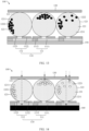
- a common electronic ink screen includes two substrates 210, and electronic ink including a large quantity of microcapsule structures 123 is provided between the two substrates 210.
- the electronic ink is formed by sealing many positively charged black ink particles 1222 and many negatively charged white ink particles 1221 within the microcapsule structure 123 that is liquid inside. Because the ink particles of different colors move to different directions due to different applied electric fields, the ink particles of different colors are arranged in an orderly manner, so that a clear black and white visualization effect is presented.
- the black ink particles 1222 and the white ink particles 1221 carry different charges, when moving in the microcapsule structure 123 that is liquid inside, the black ink particles and the white ink particles interfere with each other, resulting in a slow refreshing speed of the electronic ink screen and a long response time of the electronic ink screen.
- embodiments of this application provide a new electronic ink screen 100 to resolve the foregoing technical problem.
- the electronic ink screen 100 may be applicable to a solution of a microcapsule structure 123 (refer to FIG. 2 ), and may alternatively be applicable to a solution of a microcup structure 124 (refer to FIG. 3 ). This is not limited in embodiments of this application.
- an ink display layer may include a plurality of microcapsule structures 123. Internal space of each microcapsule structure 123 forms an ink accommodating cavity 121, and a plurality of white ink particles 1221 are provided in each ink accommodating cavity 121.
- an ink display layer may include a plurality of microcup structures 124. Internal space of each microcup structure 124 forms an ink accommodating cavity 121, and a plurality of white ink particles 1221 are provided in each ink accommodating cavity 121.
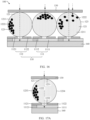
- the electronic ink screen 100 may include at least the following which are stacked: a first conductive substrate 110, an ink display layer and a second conductive substrate 130.
- the ink display layer is located between the first conductive substrate 110 and the second conductive substrate 130, and the second conductive substrate 130 is located above the first conductive substrate 110.
- a material of the second conductive substrate 130 may be indium tin oxide (Indium tin oxide, ITO).
- ITO indium tin oxide
- the indium tin oxide has good conductivity and transparency.
- the ink display layer may have a plurality of ink accommodating cavities 121 that are mutually independent.
- a plurality of ink particles that have a same color are provided in the ink accommodating cavity 121.
- the ink particles are used for displaying a first color.
- a plurality of black ink particles 1222 may be provided in each ink accommodating cavity 121.
- a plurality of white ink particles 1221 may be provided in each ink accommodating cavity 121 (refer to FIG. 2 ).
- electrophoretic base liquid 1211 may also be provided in the ink accommodating cavity 121.
- the electrophoretic base liquid 1211 is in a transparent state.
- the ink particles (for example, the white ink particles in FIG. 2 ) move freely in the electrophoretic base liquid 1211.
- the electronic ink screen 100 may further include a function layer.
- the function layer is configured to display a second color.
- the function layer may be located at a side that is of the ink display layer and that faces away from the second conductive substrate 130.
- a color displayed by the electronic ink screen 100 is a color presented by the ink particles in the ink accommodating cavity 121 (that is, the first color).
- a color displayed by the electronic ink screen 100 is a color generated by the function layer (that is, a second color).
- the plurality of ink particles in each ink accommodating cavity 121 are dispersedly provided in the ink accommodating cavity 121.
- a color displayed by the electronic ink screen 100 is between the first color and the second color. That is, the electronic ink screen 100 displays in a gray state.
- the function layer may be a black matrix layer 140.
- the ink particles may be white ink particles 1221.
- the plurality of white ink particles 1221 in each ink accommodating cavity 121 move to the inner side wall (for example, an inner front side wall, an inner back side wall, an inner left side wall 1233, or inner right side wall 1234) close to the ink accommodating cavity 121.
- the plurality of white ink particles 1221 in the ink accommodating cavity 121 move to the inner left side wall 1233 close to the ink accommodating cavity 121.
- sunlight passes through the microcapsule structure 123, shines downward, and is absorbed by the black matrix layer 140.
- a color displayed by the electronic ink screen 100 is a color of the black matrix layer 140. That is, the electronic ink screen 100 in is a black state.
- the plurality of white ink particles 1221 in each ink accommodating cavity 121 move to the inner top wall 1231 or the inner bottom wall 1232 close to the ink accommodating cavity 121.
- the plurality of white ink particles 1221 in the ink accommodating cavity 121 move to the inner top wall 1231 close to the ink accommodating cavity 121.
- the sunlight passes through the microcapsule structure 123, shines downward, and is reflected by the white ink particles 1221.
- a color displayed by the electronic ink screen 100 is a color presented by the white ink particles 1221. That is, the electronic ink screen 100 in is a white state.
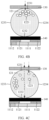
- the plurality of white ink particles 1221 in each ink accommodating cavity 121 are dispersedly provided in the ink accommodating cavity 121 (refer to FIG. 4C ).
- the electronic ink screen 100 displays in a gray state.
- this embodiment of this application it only needs to provide the plurality of white ink particles 1221 in each ink accommodating cavity 121, and apply the electric fields in different directions, to enable the electronic ink screen 100 to present states of different colors.
- a black matrix is a light-absorbing material
- a material used by the black matrix (Black Matrix, BM) layer may be any one or more of chromium (Cr, Crox) or black resin (Black Resin).
- the first conductive substrate 110 may include a drive layer 111 and an electrode layer.
- the drive layer 111 provides a voltage for the electrode layer, to form an electric field in the vertical direction and an electric field in the horizontal direction.
- a material of the electrode layer may be indium tin oxide.
- the indium tin oxide is used as a transparent electrode material, and light transmittance of the indium tin oxide may be at least 90%.
- the electrode layer may include at least one electrode group 112, and each ink accommodating cavity 121 corresponds to one electrode group 112.
- each electrode group 112 may include a first electrode 1121 and a second electrode 1122.
- the first electrode 1121 and the second electrode 1122 are disposed relative to each other in a thickness direction perpendicular to the electronic ink screen 100.
- the drive layer 111 provides a voltage for the electrode group 112, so that an electric field in the vertical direction is formed between the electrode group 112 and the second conductive substrate 130, and an electric field in the horizontal direction is formed between the first electrode 1121 and the second electrode 1122.
- the electric field in the vertical direction is used for controlling the white ink particles 1221 to move in the vertical direction in the ink accommodating cavity 121.
- the electric field in the horizontal direction is used for controlling the white ink particles 1221 to move in the horizontal direction in the ink accommodating cavity 121.
- the drive layer 111 provides a voltage for the electrode group 112, to enable an electric potential difference to be formed between the electrode group 112 and the second conductive substrate 130, to form the electric field in the vertical direction between the electrode group 112 and the second conductive substrate 130.
- the drive layer 111 provides a voltage for the first electrode 1121 separately, to enable an electric potential difference to be formed between the first electrode 1121 and the second conductive substrate 130, to form the electric field in the vertical direction between the electrode group 112 and the second conductive substrate 130.
- the drive layer 111 provides a voltage for the second electrode 1122 separately, to enable an electric potential difference to be formed between the second electrode 1122 and the second conductive substrate 130, to form the electric field in the vertical direction between the electrode group 112 and the second conductive substrate 130.
- the drive layer 111 provides voltages for both the first electrode 1121 and the second electrode 1122, to enable electric potential differences to be formed between the first electrode 1121 and the second conductive substrate 130 and between the second electrode 1122 and the second conductive substrate 130, to form the electric field in the vertical direction between the electrode group 112 and the second conductive substrate 130.
- the drive layer 111 provides voltages for both the first electrode 1121 and the second electrode 1122, so that the white ink particles 1221 move to the inner top wall 1231 or the inner bottom wall 1232 close to the ink accommodating cavity 121 is used, and when all of the white ink particles 1221 need to be located at the inner top wall 1231 or the inner bottom wall 1232 close to the ink accommodating cavity 1021, that is, the electronic ink screen 100 is in a black state, the voltages applied to the first electrode 1121 and the second electrode 1122 may be same.
- the voltages applied to the first electrode 1121 and the second electrode 1122 may be different.
- the first electrode 1121 and the second electrode 1122 are disposed relative to each other in the thickness direction perpendicular to the electronic ink screen 100. That is, the first electrode 1121 and the second electrode 1122 are disposed relative to each other in the horizontal direction.
- the drive layer 111 provides a voltage for the electrode group 112
- the drive layer 111 provides a voltage for the first electrode 1121 separately
- an electric potential difference is enabled to be formed between the first electrode 1121 and the second electrode 1122, to form the electric field in the horizontal direction between the first electrode 1121 and the second electrode 1122.
- the drive layer 111 provides a voltage for the second electrode 1122 separately, to enable an electric potential difference to be formed between the first electrode 1121 and the second electrode 1122, to form the electric field in the horizontal direction between the first electrode 1121 and the second electrode 1122.
- the drive layer 111 provides voltages in different magnitudes for both the first electrode 1121 and the second electrode 1122, to enable an electric potential difference to be formed between the first electrode 1121 and the second electrode 1122, to form the electric field in the horizontal direction between the first electrode 1121 and the second electrode 1122.
- an electric potential difference is enabled to be formed between the first electrode 1121 and the second conductive substrate 130, to form the electric field in the vertical direction between the electrode group 112 and the second conductive substrate 130, and an electric potential difference is alternatively enabled to be formed between the first electrode 1121 and the second electrode 1122, to form the electric field in the horizontal direction between the first electrode 1121 and the second electrode 1122.
- a voltage value may be flexibly adjusted based on an actual distance between the first electrode 1121 and the second conductive substrate 130 and an actual distance between the first electrode 1121 and the second electrode 1122, to enable the electric field in the vertical direction to be formed only between the electrode group 112 and the second conductive substrate 130, or to enable the electric field in the horizontal direction to be formed only between the first electrode 1121 and the second electrode 1122.
- a distance between the first electrode 1121 and the second conductive substrate 130 is large, and a distance between the first electrode 1121 and the second electrode 1122 is small.
- the electric field in the horizontal direction is formed between the first electrode 1121 and the second electrode 1122.
- the electric field in the vertical direction is formed between the electrode group 112 and the second conductive substrate 130.
- positive polarity and negative polarity of the voltage provided by the drive layer 111 for the electrode group 112 may affect an actual state of motion of the white ink particles 1221.
- the white ink particles 1221 carry negative charges.
- An example in which the electric field in the vertical direction is formed between the electrode group 112 and the second conductive substrate 130 is used.
- the voltage provided by the drive layer 111 for the electrode group 112 is a positive voltage
- an electric potential value of the electrode group 112 is larger than an electric potential value of the second conductive substrate 130.
- an electric potential difference is formed between the electrode group 112 and the second conductive substrate 130
- the electric field in the vertical direction is formed between the electrode group 112 and the second conductive substrate 130.
- the electric field is generated starting from the electrode group 112 and extending in a direction toward the second conductive substrate 130 (that is, from bottom to top). Because the white ink particles 1221 carry the negative charges, the white ink particles 1221 move to the inner bottom wall 1232 close to the ink accommodating cavity 121. In this case, the electronic ink screen 100 is in a white state.
- an electric potential value of the electrode group 112 is smaller than an electric potential value of the second conductive substrate 130. In this way, an electric potential difference is formed between the electrode group 112 and the second conductive substrate 130, and the electric field in the vertical direction is formed between the electrode group 112 and the second conductive substrate 130.
- the electric field is generated starting from the second conductive substrate 130 and extending in a direction toward the electrode group 112 (that is, from top to bottom). Because the white ink particles 1221 carry the negative charges, the white ink particles 1221 move to the inner top wall 1231 close to the ink accommodating cavity 121. in this case, the electronic ink screen 100 is also in a white state.
- the electric field in the horizontal direction is formed between the first electrode 1121 and the second electrode 1122 .
- the voltage provided by the drive layer 111 for the first electrode 1121 is a positive voltage
- an electric potential value of the first electrode 1121 is larger than an electric potential value of the second electrode 1122.
- an electric potential difference is formed between the first electrode 1121 and the second electrode 1122
- the electric field in the horizontal direction is formed between the first electrode 1121 and the second electrode 1122.
- the electric field is generated starting from the first electrode 1121 and extending in a direction toward the second electrode 1122 (that is, from left to right). Because the white ink particles 1221 carry the negative charges, the white ink particles 1221 move to a left side wall close to the ink accommodating cavity 121. In this case, the electronic ink screen 100 is in a black state.
- an electric potential value of the first electrode 1121 is smaller than an electric potential value of the second electrode 1122. In this way, an electric potential difference is formed between the first electrode 1121 and the second electrode 1122, and the electric field in the horizontal direction is formed between the first electrode 1121 and the second electrode 1122.
- the electric field is generated starting from the second electrode 1122 and extending in a direction toward the first electrode 1121 (that is, from right to left). Because the white ink particles 1221 carry the negative charges, the white ink particles 1221 move to a right side wall close to the ink accommodating cavity 121. In this case, the electronic ink screen 100 is also in a black state.
- the drive layer 111 may include a substrate layer 1111 and at least one drive switch 1112.
- the at least one drive switch 1112 is located above the substrate layer 1111, and the at least one drive switch 1112 is configured to provide a voltage for the electrode group 112.
- the drive switch 1112 may be a thin film transistor (Thin Film Transistor, TFT).
- TFT Thin Film Transistor
- the thin film transistor means that each liquid crystal pixel point on a liquid crystal display is driven by the thin film transistor integrated behind the liquid crystal pixel point. In this way, screen information can be displayed in high speed, high brightness, and high contrast.
- a quantity of the drive switches 1112 corresponding to each microcapsule structure 123 is one.
- the drive switch 1112 provides a voltage for the first electrode 1121.
- the drive switch 1112 provides a voltage for the second electrode 1122.
- the drive switch 1112 provides a voltage for the first electrode 1121 separately, to enable an electric potential difference to be formed between the first electrode 1121 and the second electrode 1122, to form the electric field in the horizontal direction between the first electrode 1121 and the second electrode 1122.
- the drive switch 1112 provides a voltage for the second electrode 1122 separately, to enable an electric potential difference to be also formed between the first electrode 1121 and the second electrode 1122, to form the electric field in the horizontal direction between the first electrode 1121 and the second electrode 1122.
- a quantity of the drive switch 1112 corresponding to each microcapsule structure 123 is two.
- One of the two drive switches 1112 provides a voltage for the first electrode 1121
- the other of the two drive switches 1112 provides a voltage for the second electrode 1122.
- the opened drive switch 1112 may provide a voltage for the first electrode 1121 separately, to enable an electric potential difference to be formed between the first electrode 1121 and the second electrode 1122, to form the electric field in the horizontal direction between the first electrode 1121 and the second electrode 1122.
- the opening drive switch 1112 may provide a voltage for the second electrode 1122 separately, to enable an electric potential difference to be formed between the first electrode 1121 and the second electrode 1122, to form the electric field in the horizontal direction between the first electrode 1121 and the second electrode 1122.
- the two drive switches 1112 may provide voltages in different magnitudes for the first electrode 1121 and the second electrode 1122 respectively, to enable the electric potential difference to be formed between the first electrode 1121 and the second electrode 1122, to form the electric field in the horizontal direction between the first electrode 1121 and the second electrode 1122.
- the drive layer 111 in a first drive state, that is, the drive layer 111 provides a voltage for the electrode group 112 (at least one of the first electrode 1121 and the second electrode 1122), the electric field in the horizontal direction may be formed between the first electrode 1121 and the second electrode 1122.
- the white ink particles 1221 move to the inner side wall close to the ink accommodating cavity 121, and the electronic ink screen 100 displays a black color.
- the drive layer 111 provides a voltage for the electrode group 112 (at least one of the first electrode 1121 and the second electrode 1122), the electric field in the vertical direction is formed between the electrode group 112 and the second conductive substrate 130, and the white ink particles 1221 move to the inner top wall 1231 or the inner bottom wall 1232 close to the ink accommodating cavity 121.
- the electronic ink screen 100 displays a white color.
- the drive layer 111 provides a voltage for the electrode group 112 (at least one of the first electrode 1121 and the second electrode 1122), the electric field in the horizontal direction is formed between the first electrode 1121 and the second electrode 1122, the electric field in the vertical direction is formed between the electrode group 112 and the second conductive substrate 130, the white ink particles 1221 are dispersedly provided in the ink accommodating cavity 121, and the electronic ink screen 100 displays in a gray state.
- the black matrix layer 140 may be located between the ink display layer and the first conductive substrate 110 (refer to FIG. 2 ). Alternatively, as shown in FIG. 6 , the black matrix layer 140 may be located between the electrode layer and the drive layer 111.
- the electrode group 112 is connected to the drive layer 111 by an electrode lead (not shown), and the drive layer 111 provides a voltage for the electrode group 112 through the electrode lead.
- first through holes 141 (refer to FIG. 7 ) are needed to be provided on the black matrix layer 140, so that the electrode lead passes through the first through holes 141 on the black matrix layer 140 to implement providing, by the drive layer 111, a voltage for the electrode group 112.
- the black matrix layer 140 may alternatively be located at a side that is of the first conductive substrate 110 and that faces away from the second conductive substrate 130. This is not limited in this embodiment of this application.
- the electronic ink screen 100 when displaying in the gray state, may present various different forms of gray scale. Specifically, a magnitude of intensity of the electric field may be adjusted based on quantitative control on an applied voltage, to enable the electronic ink screen 100 to display different shades of gray states.
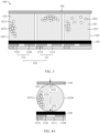
- FIG. 9 shows three different forms of gray scale (that is, a first gray state D 1, a second gray state D2, and a third gray state D3). As shown in FIG. 9 , from left to right, a color of the gray state displayed by the electronic ink screen 100 becomes increasingly dark.
- An embodiment of this application further provides an electronic ink screen 100 with another structure.
- Embodiment 2 Compared with Embodiment 2, a difference between Embodiment 2 and Embodiment 2 lies in that specific materials of function layers are different.
- a function layer may be a reflective metal layer 150, and ink particles may be black ink particles 1222.
- a plurality of black ink particles 1222 in each ink accommodating cavity 121 move to an inner side wall close to the ink accommodating cavity 121.
- the plurality of black ink particles 1222 in the ink accommodating cavity 121 move to an inner left side wall 1233 close to the ink accommodating cavity 121.
- sunlight passes through a microcapsule structure 123, shines downward, and is absorbed by the reflective metal layer 150.
- a color displayed by the electronic ink screen 100 is a white color, that is, the electronic ink screen 100 in is a white state.
- the plurality of black ink particles 1222 in each ink accommodating cavity 121 move to an inner top wall 1231 or an inner bottom wall 1232 close to the ink accommodating cavity 121.
- the plurality of black ink particles 1222 in the ink accommodating cavity 121 move to the inner top wall 1231 close to the ink accommodating cavity 121.
- the sunlight passes through the microcapsule structure 123, and shines downward, and is absorbed by the black ink particles 1222.
- a color displayed by the electronic ink screen 100 is a color presented by the black ink particles 1222. That is, the electronic ink screen 100 in is a black state.
- the plurality of black ink particles 1222 in each ink accommodating cavity 121 are dispersedly provided in the ink accommodating cavity 121 (refer to FIG. 11C ).
- the electronic ink screen 100 displays in a gray state.
- the reflective metal layer 150 may be located between an electrode layer and a drive layer 111 (refer to FIG. 10 ).
- An electrode group 112 is connected to the drive layer 111 by an electrode lead (not shown), and the drive layer 111 provides a voltage for the electrode group 112 through the electrode lead.
- second through holes 151 are needed to be provided on the reflective metal layer 150 (refer to FIG. 12 ), so that the electrode lead passes through the second through holes 151 on the reflective metal layer 150 to implement providing, by the drive layer 111, a voltage for the electrode group 112.
- the reflective metal layer 150 may be located at a side that is of the first conductive substrate 110 and that faces away from a second conductive substrate 130. This is not limited in this embodiment of this application.
- a material used by the reflective metal layer 150 may be aluminum or silver.
- a first drive state that is, the drive layer 111 provides a voltage for the electrode group 112 (at least one of a first electrode 1121 and a second electrode 1122)
- an electric field in a horizontal direction may be formed between the first electrode 1121 and the second electrode 1122.
- the black ink particles 1222 move to the inner side wall close to the ink accommodating cavity 121, and the electronic ink screen 100 displays a white color.
- the drive layer 111 provides a voltage for the electrode group 112 (at least one of the first electrode 1121 and the second electrode 1122)
- the electric field in the vertical direction is formed between the electrode group 112 and a second conductive substrate 130.
- the black ink particles 1222 move to the inner top wall 1231 or the inner bottom wall 1232 close to the ink accommodating cavity 121, and the electronic ink screen 100 displays a black color.
- the drive layer 111 provides a voltage for the electrode group 112 (at least one of the first electrode 1121 and the second electrode 1122), the electric field in the horizontal direction is formed between the first electrode 1121 and the second electrode 1122, the electric field in the vertical direction is formed between the electrode group 112 and the second conductive substrate 130, the black ink particles 1222 are dispersedly provided in the ink accommodating cavity 121, and the electronic ink screen displays 100 in a gray state.
- An embodiment of this application further provides an electronic ink screen 100 with another structure.
- Embodiment 1 and Embodiment 2 Compared with Embodiment 1 and Embodiment 2, a difference between Embodiment 3 and Embodiment 1 and Embodiment 2 lies in that specific materials of function layers are different.
- a function layer may be a display screen 160.
- the display screen 160 may be an organic light-emitting diode display screen 160 (Organic Light-Emitting Diode, OLED), or a liquid crystal display 160 (Liquid Crystal Display, LCD).
- OLED Organic Light-Emitting Diode
- LCD Liquid Crystal Display
- ink particles may be white ink particles 1221, and the display screen 160 may be in a black state.
- a color displayed by the electronic ink screen 100 is a color displayed by the organic light-emitting diode display screen 160 or the liquid crystal display 160. That is, the electronic ink screen 100 is in a black state.
- the plurality of white ink particles 1221 in each ink accommodating cavity 121 move to an inner top wall 1231 or an inner bottom wall 1232 close to the ink accommodating cavity 121.
- the plurality of white ink particles 1221 in each ink accommodating cavity 121 move to the inner top wall 1231 close to the ink accommodating cavity 121.
- a color displayed by the electronic ink screen 100 is a color presented by the white ink particles 1221. That is, the electronic ink screen 100 in is a white state.
- the plurality of white ink particles 1221 in each ink accommodating cavity 121 are dispersedly provided in the ink accommodating cavity 121 (refer to FIG. 15C ).
- the electronic ink screen 100 displays in a gray state.
- the display screen 160 may be located at a side that is of the first conductive substrate 110 and that faces away from an ink display layer.
- a drive layer 111 provides a voltage for an electrode group 112 (at least one of a first electrode 1121 and a second electrode 1122), an electric field in a horizontal direction is formed between the first electrode 1121 and a second electrode 1122, the white ink particles 1221 move to the inner side wall close to the ink accommodating cavity 121, and the electronic ink screen 100 displays a black color.
- the drive layer 111 provides a voltage for the electrode group 112 (at least one of the first electrode 1121 and the second electrode 1122), the electric field in the vertical direction is formed between the electrode group 112 and a second conductive substrate 130, the white ink particles 1221 move to the inner top wall 1231 or the inner bottom wall 1232 close to the ink accommodating cavity 121, and the electronic ink screen 100 displays a white color.
- the drive layer 111 provides a voltage for the electrode group 112 (at least one of the first electrode 1121 and the second electrode 1122), the electric field in the horizontal direction is formed between the first electrode 1121 and the second electrode 1122, the electric field in the vertical direction is formed between the electrode group 112 and the second conductive substrate 130, the white ink particles 1221 are dispersedly provided in the ink accommodating cavity 121, and the electronic ink screen 100 displays in a gray state.
- An embodiment of this application further provides an electronic ink screen 100 with another structure.
- a difference between Embodiment 4 and Embodiment 3 lies in that when a function layer is a display screen 160, a display state of the display screen 160 is not the same.
- ink particles may be black ink particles 1222, and the display screen 160 may be in a display state.
- a color displayed by the electronic ink screen 100 is a color displayed by an organic light-emitting diode display screen 160 or a liquid crystal display 160. That is, the electronic ink screen 100 is in the display state (for example, a white state).
- the plurality of black ink particles 1222 in each ink accommodating cavity 121 move to an inner top wall 1231 or an inner bottom wall 1232 close to the ink accommodating cavity 121.
- the plurality of black ink particles 1222 in the ink accommodating cavity 121 move to the inner top wall 1231 close to the ink accommodating cavity 121.
- a color displayed by the electronic ink screen 100 is a color presented by the black ink particles 1222. That is, the electronic ink screen 100 in is a black state.
- the plurality of black ink particles 1222 in each ink accommodating cavity 121 are dispersedly provided in the ink accommodating cavity 121 (refer to FIG. 17C ).
- the electronic ink screen 100 displays in a gray state.
- a drive layer 111 provides a voltage for an electrode group 112 (at least one of a first electrode 1121 and a second electrode 1122), an electric field in a horizontal direction is formed between the first electrode 1121 and the second electrode 1122, the black ink particles 1222 move to the inner side wall close to the ink accommodating cavity 121, and the electronic ink screen 100 displays a white color.
- the drive layer 111 provides a voltage for the electrode group 112 (at least one of the first electrode 1121 and the second electrode 1122), the electric field in the vertical direction is formed between the electrode group 112 and a second conductive substrate 130, the black ink particles 1222 move to the inner top wall 1231 or the inner bottom wall 1232 close to the ink accommodating cavity 121, and the electronic ink screen 100 displays a black color.
- the drive layer 111 provides a voltage for the electrode group 112 (at least one of the first electrode 1121 and the second electrode 1122), the electric field in the horizontal direction is formed between the first electrode 1121 and the second electrode 1122, the electric field in the vertical direction is formed between the electrode group 112 and the second conductive substrate 130, the black ink particles 1222 are dispersedly provided in the ink accommodating cavity 121, and the electronic ink screen displays 100 in a gray state.
- the electronic ink screen 100 can only support simple colors and gray scales.
- the electronic ink screen 100 can only display two colors of black and white, but cannot display rich colors, resulting poor user experience.
- a display color of the display screen 160 may be designed to different colors, such as light yellow, light blue and light green, to enlarge a display color gamut of the ink display screen 160.
- display states of an ink display layer and the display screen 160 are flexibly switched, which facilitates the ink display screen 160 to achieve a display effect of a full color gamut.
- an embodiment of this application provides a display apparatus.
- the display apparatus may includes at least the electronic ink screen 100 in any one of the foregoing embodiments.
- the display apparatus may be various products or components that have a display function, such as an electronic label, an electronic book, a wearable device (for example, a watch), an electronic reader, a navigator, an electronic photo frame, a home appliance (for example, an alarm clock in a double-sided display or a transparent display manner), and a billboard of a supermarket.
- a display function such as an electronic label, an electronic book, a wearable device (for example, a watch), an electronic reader, a navigator, an electronic photo frame, a home appliance (for example, an alarm clock in a double-sided display or a transparent display manner), and a billboard of a supermarket.
- a specific application scenario of an ink display screen 160 is not limited in this embodiment of this application.
- the display apparatus may include the ink display screen 160.
- a function layer is disposed at a side that is of an ink display layer and that faces away from a second conductive substrate 130.
- a plurality of ink particles of each ink accommodating cavity 121 move to an inner side wall close to the ink accommodating cavity 121.
- a color displayed by the electronic ink screen 100 is a color generated by the function layer.
- the plurality of ink particles in each ink accommodating cavity 121 move to an inner top wall 1231 or an inner bottom wall 1232 close to the ink accommodating cavity 121.
- a color displayed by the electronic ink screen 100 is a color presented by the ink particles in the ink accommodating cavity 121.
- the electronic ink screen 100 displays in a gray state. Therefore, in this embodiment of this application, it only needs to provide the plurality of ink particles with a same color in each ink accommodating cavity 121, and apply the electric fields in different directions, to enable the electronic ink screen 100 to present states of different colors. This avoids a problem of motion interference generated by switches between ink particles of two different colors in the prior art, so that a refreshing speed of the electronic ink screen 100 can be improved, thereby reducing a response time of the electronic ink screen 100.
- the display apparatus also has an advantage of low power consumption compared with a liquid crystal display apparatus, an OLED display apparatus, and the like in the prior art.
- Embodiment 1 Embodiment 1, Embodiment 2, Embodiment 3, and Embodiment 4, and a same technical effect can be achieved. Details are not described herein again.
- connection should be understood broadly.
- the connection may be a fixed connection, an indirect connection through an intermediary, or internal communication between two components or mutual interaction relationship between two components.
- a person of ordinary skill in the art may understand specific meanings of the foregoing terms in embodiments of this application based on specific situations.
Landscapes
- Physics & Mathematics (AREA)
- Nonlinear Science (AREA)
- General Physics & Mathematics (AREA)
- Optics & Photonics (AREA)
- Health & Medical Sciences (AREA)
- Life Sciences & Earth Sciences (AREA)
- Chemical & Material Sciences (AREA)
- Chemical Kinetics & Catalysis (AREA)
- Electrochemistry (AREA)
- Molecular Biology (AREA)
- Electrochromic Elements, Electrophoresis, Or Variable Reflection Or Absorption Elements (AREA)
- Devices For Indicating Variable Information By Combining Individual Elements (AREA)
Applications Claiming Priority (2)
| Application Number | Priority Date | Filing Date | Title |
|---|---|---|---|
| CN202111408661.4A CN115047686B (zh) | 2021-11-24 | 2021-11-24 | 电子墨水屏及显示装置 |
| PCT/CN2022/112207 WO2023093135A1 (fr) | 2021-11-24 | 2022-08-12 | Écran d'encre électronique et appareil d'affichage |
Publications (1)
| Publication Number | Publication Date |
|---|---|
| EP4328668A1 true EP4328668A1 (fr) | 2024-02-28 |
Family
ID=83156262
Family Applications (1)
| Application Number | Title | Priority Date | Filing Date |
|---|---|---|---|
| EP22897230.3A Pending EP4328668A1 (fr) | 2021-11-24 | 2022-08-12 | Écran d'encre électronique et appareil d'affichage |
Country Status (3)
| Country | Link |
|---|---|
| EP (1) | EP4328668A1 (fr) |
| CN (1) | CN115047686B (fr) |
| WO (1) | WO2023093135A1 (fr) |
Families Citing this family (1)
| Publication number | Priority date | Publication date | Assignee | Title |
|---|---|---|---|---|
| CN116794895B (zh) * | 2023-08-28 | 2023-11-28 | 苏州华星光电技术有限公司 | 显示面板及显示装置 |
Family Cites Families (11)
| Publication number | Priority date | Publication date | Assignee | Title |
|---|---|---|---|---|
| ATE320022T1 (de) * | 2002-10-18 | 2006-03-15 | Koninkl Philips Electronics Nv | Elektrophoretische anzeigevorrichtung |
| WO2006015044A1 (fr) * | 2004-07-27 | 2006-02-09 | E Ink Corporation | Affichages electro-optiques |
| KR101437164B1 (ko) * | 2007-12-20 | 2014-09-03 | 삼성전자주식회사 | 전기영동 표시 소자 및 그 구동 방법 |
| US8797634B2 (en) * | 2010-11-30 | 2014-08-05 | E Ink Corporation | Multi-color electrophoretic displays |
| CN103576405A (zh) * | 2012-08-09 | 2014-02-12 | 余志刚 | 电子墨水纸与液晶显示器混合使用的显示装置 |
| KR20140039570A (ko) * | 2012-09-24 | 2014-04-02 | 한국전자통신연구원 | 컬러 전자종이 디스플레이 및 그 제조 방법 |
| CN103353701B (zh) * | 2013-07-22 | 2015-08-19 | 京东方科技集团股份有限公司 | 一种显示面板、显示装置、显示面板制作方法及显示方法 |
| CN105652552A (zh) * | 2015-12-30 | 2016-06-08 | 联想(北京)有限公司 | 一种电子墨水屏和电子设备 |
| CN106773016B (zh) * | 2017-01-03 | 2019-01-18 | 京东方科技集团股份有限公司 | 一种显示面板及其刷屏方法 |
| CN110967889A (zh) * | 2019-12-23 | 2020-04-07 | Tcl华星光电技术有限公司 | 显示面板 |
| CN113156732A (zh) * | 2021-05-31 | 2021-07-23 | 京东方科技集团股份有限公司 | 反射式显示面板及其制备方法、及显示装置 |
-
2021
- 2021-11-24 CN CN202111408661.4A patent/CN115047686B/zh active Active
-
2022
- 2022-08-12 WO PCT/CN2022/112207 patent/WO2023093135A1/fr active Application Filing
- 2022-08-12 EP EP22897230.3A patent/EP4328668A1/fr active Pending
Also Published As
| Publication number | Publication date |
|---|---|
| WO2023093135A9 (fr) | 2023-09-21 |
| CN115047686A (zh) | 2022-09-13 |
| CN115047686B (zh) | 2023-05-09 |
| WO2023093135A1 (fr) | 2023-06-01 |
Similar Documents
| Publication | Publication Date | Title |
|---|---|---|
| Bai et al. | Review of paper-like display technologies (invited review) | |
| US9881565B2 (en) | Method for driving electro-optic displays | |
| US8902152B2 (en) | Dual sided electrophoretic display | |
| US20170200424A1 (en) | Transparent display assembly and display device | |
| CN102289127B (zh) | 显示装置及其制造方法 | |
| US20240027835A1 (en) | Display panel and electronic device | |
| CN109920831B (zh) | 一种显示面板及其驱动方法、显示装置 | |
| JP2013041099A (ja) | 透明ディスプレイ装置 | |
| US20190206307A1 (en) | Display with switchable background appearance | |
| EP4328668A1 (fr) | Écran d'encre électronique et appareil d'affichage | |
| CN105676444B (zh) | 一种电润湿双稳态电流体显示装置 | |
| US6556334B2 (en) | Flat panel display using microelectromechanical device | |
| CN105223726B (zh) | 彩色滤光片基板及制作方法和液晶显示装置及驱动方法 | |
| CN102262327A (zh) | 图像显示系统 | |
| JP2004341156A (ja) | ディスプレイ装置 | |
| US8797635B2 (en) | Color electrophoretic display | |
| JP2013041100A (ja) | 透明ディスプレイ装置 | |
| US20060256421A1 (en) | Electrophoretic display device | |
| CN101154008A (zh) | 电子纸装置 | |
| Rawert et al. | 15.2: Bistable D3 Electrowetting Display Products and Applications | |
| US20210405467A1 (en) | Display device | |
| CN202383397U (zh) | 双面显示电子纸及电子纸显示器 | |
| CN211016463U (zh) | 一种显示装置 | |
| WO2011070769A1 (fr) | Panneau d'affichage d'informations et son procédé de fabrication | |
| CN217561884U (zh) | 一种显示装置 |
Legal Events
| Date | Code | Title | Description |
|---|---|---|---|
| STAA | Information on the status of an ep patent application or granted ep patent |
Free format text: STATUS: THE INTERNATIONAL PUBLICATION HAS BEEN MADE |
|
| PUAI | Public reference made under article 153(3) epc to a published international application that has entered the european phase |
Free format text: ORIGINAL CODE: 0009012 |
|
| STAA | Information on the status of an ep patent application or granted ep patent |
Free format text: STATUS: REQUEST FOR EXAMINATION WAS MADE |
|
| 17P | Request for examination filed |
Effective date: 20231123 |
|
| AK | Designated contracting states |
Kind code of ref document: A1 Designated state(s): AL AT BE BG CH CY CZ DE DK EE ES FI FR GB GR HR HU IE IS IT LI LT LU LV MC MK MT NL NO PL PT RO RS SE SI SK SM TR |