EP4326015A1 - Pcb pad for smt process - Google Patents
Pcb pad for smt process Download PDFInfo
- Publication number
- EP4326015A1 EP4326015A1 EP22206714.2A EP22206714A EP4326015A1 EP 4326015 A1 EP4326015 A1 EP 4326015A1 EP 22206714 A EP22206714 A EP 22206714A EP 4326015 A1 EP4326015 A1 EP 4326015A1
- Authority
- EP
- European Patent Office
- Prior art keywords
- pcb
- insulation body
- metal
- pcb pad
- disclosure
- Prior art date
- Legal status (The legal status is an assumption and is not a legal conclusion. Google has not performed a legal analysis and makes no representation as to the accuracy of the status listed.)
- Pending
Links
Images




Classifications
-
- H—ELECTRICITY
- H05—ELECTRIC TECHNIQUES NOT OTHERWISE PROVIDED FOR
- H05K—PRINTED CIRCUITS; CASINGS OR CONSTRUCTIONAL DETAILS OF ELECTRIC APPARATUS; MANUFACTURE OF ASSEMBLAGES OF ELECTRICAL COMPONENTS
- H05K1/00—Printed circuits
- H05K1/02—Details
- H05K1/11—Printed elements for providing electric connections to or between printed circuits
- H05K1/111—Pads for surface mounting, e.g. lay-out
-
- H—ELECTRICITY
- H05—ELECTRIC TECHNIQUES NOT OTHERWISE PROVIDED FOR
- H05K—PRINTED CIRCUITS; CASINGS OR CONSTRUCTIONAL DETAILS OF ELECTRIC APPARATUS; MANUFACTURE OF ASSEMBLAGES OF ELECTRICAL COMPONENTS
- H05K3/00—Apparatus or processes for manufacturing printed circuits
- H05K3/30—Assembling printed circuits with electric components, e.g. with resistors
- H05K3/32—Assembling printed circuits with electric components, e.g. with resistors electrically connecting electric components or wires to printed circuits
- H05K3/34—Assembling printed circuits with electric components, e.g. with resistors electrically connecting electric components or wires to printed circuits by soldering
- H05K3/341—Surface mounted components
-
- H—ELECTRICITY
- H05—ELECTRIC TECHNIQUES NOT OTHERWISE PROVIDED FOR
- H05K—PRINTED CIRCUITS; CASINGS OR CONSTRUCTIONAL DETAILS OF ELECTRIC APPARATUS; MANUFACTURE OF ASSEMBLAGES OF ELECTRICAL COMPONENTS
- H05K1/00—Printed circuits
- H05K1/02—Details
- H05K1/0271—Arrangements for reducing stress or warp in rigid printed circuit boards, e.g. caused by loads, vibrations or differences in thermal expansion
-
- H—ELECTRICITY
- H05—ELECTRIC TECHNIQUES NOT OTHERWISE PROVIDED FOR
- H05K—PRINTED CIRCUITS; CASINGS OR CONSTRUCTIONAL DETAILS OF ELECTRIC APPARATUS; MANUFACTURE OF ASSEMBLAGES OF ELECTRICAL COMPONENTS
- H05K1/00—Printed circuits
- H05K1/18—Printed circuits structurally associated with non-printed electric components
- H05K1/181—Printed circuits structurally associated with non-printed electric components associated with surface mounted components
-
- H—ELECTRICITY
- H05—ELECTRIC TECHNIQUES NOT OTHERWISE PROVIDED FOR
- H05K—PRINTED CIRCUITS; CASINGS OR CONSTRUCTIONAL DETAILS OF ELECTRIC APPARATUS; MANUFACTURE OF ASSEMBLAGES OF ELECTRICAL COMPONENTS
- H05K2201/00—Indexing scheme relating to printed circuits covered by H05K1/00
- H05K2201/09—Shape and layout
- H05K2201/09209—Shape and layout details of conductors
- H05K2201/09654—Shape and layout details of conductors covering at least two types of conductors provided for in H05K2201/09218 - H05K2201/095
- H05K2201/09781—Dummy conductors, i.e. not used for normal transport of current; Dummy electrodes of components
-
- H—ELECTRICITY
- H05—ELECTRIC TECHNIQUES NOT OTHERWISE PROVIDED FOR
- H05K—PRINTED CIRCUITS; CASINGS OR CONSTRUCTIONAL DETAILS OF ELECTRIC APPARATUS; MANUFACTURE OF ASSEMBLAGES OF ELECTRICAL COMPONENTS
- H05K2201/00—Indexing scheme relating to printed circuits covered by H05K1/00
- H05K2201/10—Details of components or other objects attached to or integrated in a printed circuit board
- H05K2201/10007—Types of components
- H05K2201/10204—Dummy component, dummy PCB or template, e.g. for monitoring, controlling of processes, comparing, scanning
-
- H—ELECTRICITY
- H05—ELECTRIC TECHNIQUES NOT OTHERWISE PROVIDED FOR
- H05K—PRINTED CIRCUITS; CASINGS OR CONSTRUCTIONAL DETAILS OF ELECTRIC APPARATUS; MANUFACTURE OF ASSEMBLAGES OF ELECTRICAL COMPONENTS
- H05K2201/00—Indexing scheme relating to printed circuits covered by H05K1/00
- H05K2201/10—Details of components or other objects attached to or integrated in a printed circuit board
- H05K2201/10227—Other objects, e.g. metallic pieces
- H05K2201/1031—Surface mounted metallic connector elements
- H05K2201/10318—Surface mounted metallic pins
-
- H—ELECTRICITY
- H05—ELECTRIC TECHNIQUES NOT OTHERWISE PROVIDED FOR
- H05K—PRINTED CIRCUITS; CASINGS OR CONSTRUCTIONAL DETAILS OF ELECTRIC APPARATUS; MANUFACTURE OF ASSEMBLAGES OF ELECTRICAL COMPONENTS
- H05K2201/00—Indexing scheme relating to printed circuits covered by H05K1/00
- H05K2201/10—Details of components or other objects attached to or integrated in a printed circuit board
- H05K2201/10431—Details of mounted components
- H05K2201/10507—Involving several components
- H05K2201/10522—Adjacent components
-
- H—ELECTRICITY
- H05—ELECTRIC TECHNIQUES NOT OTHERWISE PROVIDED FOR
- H05K—PRINTED CIRCUITS; CASINGS OR CONSTRUCTIONAL DETAILS OF ELECTRIC APPARATUS; MANUFACTURE OF ASSEMBLAGES OF ELECTRICAL COMPONENTS
- H05K2201/00—Indexing scheme relating to printed circuits covered by H05K1/00
- H05K2201/20—Details of printed circuits not provided for in H05K2201/01 - H05K2201/10
- H05K2201/2036—Permanent spacer or stand-off in a printed circuit or printed circuit assembly
-
- H—ELECTRICITY
- H05—ELECTRIC TECHNIQUES NOT OTHERWISE PROVIDED FOR
- H05K—PRINTED CIRCUITS; CASINGS OR CONSTRUCTIONAL DETAILS OF ELECTRIC APPARATUS; MANUFACTURE OF ASSEMBLAGES OF ELECTRICAL COMPONENTS
- H05K3/00—Apparatus or processes for manufacturing printed circuits
- H05K3/30—Assembling printed circuits with electric components, e.g. with resistors
- H05K3/303—Assembling printed circuits with electric components, e.g. with resistors with surface mounted components
Definitions
- the technical field relates to a supporting pad, and more particularly relates to a printed circuit board (PCB) pad for a surface mount technology (SMT) process.
- PCB printed circuit board
- SMT surface mount technology
- some PCBs may be disposed with a plurality of PCB pads/bumpers to support the electronic components on the PCB to prevent the electronic components from being pressed.
- the related-art PCB pads/bumpers may be fixed on the PCBs by dispensing or combined with the PCB through adhering by hand after adding adhesive.
- the related-art PCB pads/bumpers fixed by adhesive may not be used in a high-temperature reflow soldering.
- the related-art PCB pads/bumpers may not be combined with the PCB by an automated machine during the soldering process.
- One object of this disclosure is to provide a PCB pad for a SMT process to support the electronic components disposed on the PCB, so that the electronic components may be prevented from damaging by the external force.
- this disclosure is a PCB pad for a SMT process and is combined on a PCB.
- the PCB pad includes an insulation body and a metal reflow portion disposed on the insulation body.
- the metal reflow portion is located on a side of the insulation body adjacent to the PCB.
- the metal reflow portion is not electrically connected with the PCB.
- the PCB pad for the SMT process in this disclosure is disposed the metal reflow portion on the insulation body, and the PCB pad is disposed on the PCB by placing the metal reflow portion in a direction close to the PCB.
- the insulation body of the PCB pad has a pick-up plane for vacuum suction by an automatic machine or an automatic arm.
- the solder may be attached on the metal reflow portion to solder the PCB pad on the PCB.
- the PCB pads may be attached to two sides of electronic components, such as surface mount device (SMD) components, for supporting. As a result, the electronic components may be prevented from being damaged by the external pressure.
- SMD surface mount device
- FIG. 1 and FIG. 2 depict a perspective exploded schematic view and a cross-sectional view of the PCB pad for the SMT process in this disclosure.
- This disclosure is a PCB pad 1 for a SMT process, the PCB pad 1 includes an insulation body 10 and a metal reflow portion 20 disposed on the insulation body 10.
- the insulation body 10 has a pick-up plane 11 used for vacuum suction by an automatic machine or an automatic arm.
- the metal reflow portion 20 includes at least one metal pin 21.
- the metal pin 21 is inserted in the insulation body 10 and exposed from the bottom 101 of the insulation body 10.
- the metal pin 21 is substantially in an L shape and the number thereof is multiple.
- the insulation body 10 is a cuboid. Additionally, the metal reflow portion 20 includes a pair of metal pins 21 in L-shape. The pair of metal pins 21 are disposed spacedly on two sides of the insulation body 10 opposite to each other.
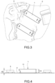
- FIG. 3 and FIG. 4 depict an application schematic view and a side view of the PCB pad for the SMT process in this disclosure.
- the PCB pad 1 of this disclosure is combined on a PCB 2 for supporting at least one electronic component 3, such as an SMD component and the like, disposed thereon.
- the PCB pads 1 may be attached to two sides of the electronic component 3, such as an SMD, component for supporting and to prevent the electronic component 3 from being damaged by an external pressure.
- the PCB pad 1 is fixed on the PCB 2.
- the insulation body 10 has a pick-up plane 11 on the side thereof away from the PCB 2.
- the automatic machine or the automatic arm may pick the PCB pad 1 by sucking the pick-up plane 11 to place the PCB pad 1 on the PCB 2.
- the PCB pad 1 is disposed on the PCB 2 by placing the metal reflow portion 20 in a direction close to the PCB 2. Since the metal reflow portion 20 is not electrically connected with the PCB 2, the arrangement of the PCB pad 1 may not affect the electrical connection of the PCB 2.
- the solder may be attached on the metal reflow portion 20 of the PCB pad 1 to solder the PCB pad 1 on the PCB 2.
- the PCB pads 1 are attached to both sides of the electronic component 3.
- the PCB pad 1 of this disclosure has an overall height H1 (the overall height is defined as the height of the PCB pad from the PCB).
- the electronic component 3 has an arranging height H2 (the arranging height is defined as the height of the electronic component from the PCB).
- the overall height H1 is greater than the arranging height H2. Accordingly, the PCB pad 1 may provide the supporting force to prevent the electronic component 3 from being damaged by an external pressure.
- the PCB pad 1a includes an insulation body 10a and a metal reflow portion 20a disposed on the insulation body 10a.
- the insulation body 10a is a cylinder and has a pick-up plane 11a.
- the metal reflow portion 20a includes a pair of L-shaped metal pins 21a. The pair of L-shaped metal pins 21a are inserted in the insulation body 10a and exposed from the bottom 101a.
- the PCB pad 1b includes an insulation body 10b and a metal reflow portion 20b disposed on the insulation body 10b.
- the insulation body 10b is a cylinder and has a pick-up plane 11b.
- the metal reflow portion 20b includes a metal pin 21b and a metal plate 22b connected to the metal pin 21b.
- the metal pin 21b is one piece formed with the metal plate 22b by punching the metal plate 22b. Additionally, a groove 102b and a slot 103b located in the groove 102b are disposed on the bottom 101b of the insulation body 10b. The metal plate 22b is attached in the groove 102b, and the metal pin 21b is inserted in the slot 103b and exposed from the bottom 101b.
- the PCB pad 1c includes an insulation body 10c and a metal reflow portion 20c disposed on the insulation body 10c.
- the insulation body 10c has a pick-up plane 11c.
- the metal reflow portion 20c is disposed on the bottom 101c of the insulation body 10c and includes a metal pin 21c disposed singly.
- the metal pins21c is in an L shape.
- the PCB pad 1d includes an insulation body 10d and a metal reflow portion 20d disposed on the insulation body 10d.
- the insulation body 10d is a cylinder and has a pick-up plane 11d.
- the metal reflow portion 20d includes an electroplating layer 21d, and the electroplating layer 21d is disposed on the bottom 101d of the insulation body 10d and extended to the side periphery 102d of the insulation body 10d.
- the PCB pad 1e includes an insulation body 10e and a metal reflow portion 20e disposed on the insulation body 10e.
- the insulation body 10e is a cube and has a pick-up plane 11e.
- the metal reflow portion 20e includes an electroplating layer 21e, and the electroplating layer 21e is only disposed on the bottom 101e of the insulation body 10e.
Landscapes
- Engineering & Computer Science (AREA)
- Microelectronics & Electronic Packaging (AREA)
- Manufacturing & Machinery (AREA)
- Electric Connection Of Electric Components To Printed Circuits (AREA)
Abstract
A PCB pad (1) for a SMT process is combined on a PCB (2). The PCB pad (1) includes an insulation body (10) and a metal reflow portion (20) disposed on the insulation body (10). The metal reflow portion (20) is located on the side of the insulation body (10) adjacent to the PCB (2). The metal reflow portion (20) is not electrically connected with the PCB (2). Thus, the PCB pad (1) may support electronic components (3) of the PCB (2) and prevent the electronic components from being damaged by an external pressure.
Description
- The technical field relates to a supporting pad, and more particularly relates to a printed circuit board (PCB) pad for a surface mount technology (SMT) process.
- In the manufacturing process of the PCB, it is usually necessary to dispose electronic components such as resistors and capacitors to achieve specific functions. In recent years, electronic components may be fixed on the PCB by SMT process.
- Moreover, some PCBs may be disposed with a plurality of PCB pads/bumpers to support the electronic components on the PCB to prevent the electronic components from being pressed. Additionally, the related-art PCB pads/bumpers may be fixed on the PCBs by dispensing or combined with the PCB through adhering by hand after adding adhesive. However, the related-art PCB pads/bumpers fixed by adhesive may not be used in a high-temperature reflow soldering. Thus, the related-art PCB pads/bumpers may not be combined with the PCB by an automated machine during the soldering process.
- In view of the above drawbacks, the inventor proposes this disclosure based on his expert knowledge and elaborate researches in order to solve the problems of related art.
- One object of this disclosure is to provide a PCB pad for a SMT process to support the electronic components disposed on the PCB, so that the electronic components may be prevented from damaging by the external force.
- In the embodiment of this disclosure, this disclosure is a PCB pad for a SMT process and is combined on a PCB. The PCB pad includes an insulation body and a metal reflow portion disposed on the insulation body. The metal reflow portion is located on a side of the insulation body adjacent to the PCB. The metal reflow portion is not electrically connected with the PCB.
- In comparison with the related art, the PCB pad for the SMT process in this disclosure is disposed the metal reflow portion on the insulation body, and the PCB pad is disposed on the PCB by placing the metal reflow portion in a direction close to the PCB. Additionally, the insulation body of the PCB pad has a pick-up plane for vacuum suction by an automatic machine or an automatic arm. Moreover, when the PCB passes the soldering machine, the solder may be attached on the metal reflow portion to solder the PCB pad on the PCB. Accordingly, the PCB pads may be attached to two sides of electronic components, such as surface mount device (SMD) components, for supporting. As a result, the electronic components may be prevented from being damaged by the external pressure.
- The features of the disclosure believed to be novel are set forth with particularity in the appended claims. The disclosure itself, however, may be best understood by reference to the following detailed description of the disclosure, which describes a number of exemplary embodiments of the disclosure, taken in conjunction with the accompanying drawings, in which:
-
FIG. 1 is a perspective exploded schematic view of the PCB pad for the SMT process in this disclosure. -
FIG. 2 is a cross-sectional view of the PCB pad for the SMT process in this disclosure. -
FIG. 3 is an application schematic view of the PCB pad for the SMT process in this disclosure. -
FIG. 4 is a side view of the PCB pad for the SMT process in this disclosure. -
FIG. 5 is a perspective exploded schematic view of another embodiment of the PCB pad for the SMT process in this disclosure. -
FIG. 6 is a cross-sectional view of another embodiment of the PCB pad for the SMT process in this disclosure. -
FIG. 7 is a perspective exploded schematic view of still another embodiment of the PCB pad for the SMT process in this disclosure. -
FIG. 8 is a cross-sectional view of still another embodiment of the PCB pad for the SMT process in this disclosure. -
FIG. 9 is a perspective exploded view of another embodiment of the PCB pad for the SMT process in this disclosure. -
FIG. 10 is a cross-sectional view of another embodiment of the PCB pad for the SMT process in this disclosure. -
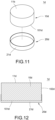
FIG. 11 is a perspective exploded view of still another embodiment of the PCB pad for the SMT process in this disclosure. -
FIG. 12 is a cross-sectional view of still another embodiment of the PCB pad for the SMT process in this disclosure. -
FIG. 13 is a perspective exploded view of another embodiment of the PCB pad for the SMT process in this disclosure. -
FIG. 14 is cross-sectional view of another embodiment of the PCB pad for the SMT process in this disclosure. - The technical contents of this disclosure will become apparent with the detailed description of embodiments accompanied with the illustration of related drawings as follows. It is intended that the embodiments and drawings disclosed herein are to be considered illustrative rather than restrictive.
- Please refer to
FIG. 1 and FIG. 2 , which depict a perspective exploded schematic view and a cross-sectional view of the PCB pad for the SMT process in this disclosure. This disclosure is aPCB pad 1 for a SMT process, thePCB pad 1 includes aninsulation body 10 and ametal reflow portion 20 disposed on theinsulation body 10. Theinsulation body 10 has a pick-up plane 11 used for vacuum suction by an automatic machine or an automatic arm. - Moreover, the
metal reflow portion 20 includes at least onemetal pin 21. Themetal pin 21 is inserted in theinsulation body 10 and exposed from thebottom 101 of theinsulation body 10. Specifically, themetal pin 21 is substantially in an L shape and the number thereof is multiple. - In one embodiment of this disclosure, the
insulation body 10 is a cuboid. Additionally, themetal reflow portion 20 includes a pair ofmetal pins 21 in L-shape. The pair ofmetal pins 21 are disposed spacedly on two sides of theinsulation body 10 opposite to each other. - Please refer to
FIG. 3 and FIG. 4 , which depict an application schematic view and a side view of the PCB pad for the SMT process in this disclosure. ThePCB pad 1 of this disclosure is combined on aPCB 2 for supporting at least oneelectronic component 3, such as an SMD component and the like, disposed thereon. In some embodiments, thePCB pads 1 may be attached to two sides of theelectronic component 3, such as an SMD, component for supporting and to prevent theelectronic component 3 from being damaged by an external pressure. - In more detail, the
PCB pad 1 is fixed on thePCB 2. Theinsulation body 10 has a pick-up plane 11 on the side thereof away from thePCB 2. Furthermore, the automatic machine or the automatic arm may pick thePCB pad 1 by sucking the pick-up plane 11 to place thePCB pad 1 on thePCB 2. - Further, in some embodiments, the
PCB pad 1 is disposed on thePCB 2 by placing themetal reflow portion 20 in a direction close to thePCB 2. Since themetal reflow portion 20 is not electrically connected with thePCB 2, the arrangement of thePCB pad 1 may not affect the electrical connection of thePCB 2. - Moreover, when the
PCB 2 passes the soldering machine, the solder may be attached on themetal reflow portion 20 of thePCB pad 1 to solder thePCB pad 1 on thePCB 2. - As shown in
FIG. 4 , in some embodiments, thePCB pads 1 are attached to both sides of theelectronic component 3. ThePCB pad 1 of this disclosure has an overall height H1 (the overall height is defined as the height of the PCB pad from the PCB). Additionally, theelectronic component 3 has an arranging height H2 (the arranging height is defined as the height of the electronic component from the PCB). The overall height H1 is greater than the arranging height H2. Accordingly, thePCB pad 1 may provide the supporting force to prevent theelectronic component 3 from being damaged by an external pressure. - Please further refer to
FIG. 5 and FIG. 6 , which depict a perspective exploded schematic view and a cross-sectional view of another embodiment of the PCB pad for the SMT process in this disclosure. In this embodiment, thePCB pad 1a includes aninsulation body 10a and ametal reflow portion 20a disposed on theinsulation body 10a. Theinsulation body 10a is a cylinder and has a pick-upplane 11a. Themetal reflow portion 20a includes a pair of L-shapedmetal pins 21a. The pair of L-shapedmetal pins 21a are inserted in theinsulation body 10a and exposed from the bottom 101a. - Please further refer to
FIG. 7 and FIG. 8 , which depict a perspective exploded schematic view and a cross-sectional view of still another embodiment of the PCB pad for the SMT process in this disclosure. In this embodiment, thePCB pad 1b includes aninsulation body 10b and ametal reflow portion 20b disposed on theinsulation body 10b. Theinsulation body 10b is a cylinder and has a pick-upplane 11b. Themetal reflow portion 20b includes ametal pin 21b and ametal plate 22b connected to themetal pin 21b. - Specifically, the
metal pin 21b is one piece formed with themetal plate 22b by punching themetal plate 22b. Additionally, agroove 102b and aslot 103b located in thegroove 102b are disposed on the bottom 101b of theinsulation body 10b. Themetal plate 22b is attached in thegroove 102b, and themetal pin 21b is inserted in theslot 103b and exposed from the bottom 101b. - Please further refer to
FIG. 9 and FIG. 10 , which depict a perspective exploded schematic view and a cross-sectional view of another embodiment of the PCB pad for the SMT process in this disclosure. In this embodiment, thePCB pad 1c includes aninsulation body 10c and ametal reflow portion 20c disposed on theinsulation body 10c. Theinsulation body 10c has a pick-upplane 11c. Themetal reflow portion 20c is disposed on the bottom 101c of theinsulation body 10c and includes ametal pin 21c disposed singly. The metal pins21c is in an L shape. - Please further refer to
FIG. 11 and FIG. 12 , which depict a perspective exploded schematic view and a cross-sectional view of still another embodiment of the PCB pad for the SMT process in this disclosure. In this embodiment, thePCB pad 1d includes aninsulation body 10d and ametal reflow portion 20d disposed on theinsulation body 10d. Theinsulation body 10d is a cylinder and has a pick-upplane 11d. Themetal reflow portion 20d includes anelectroplating layer 21d, and theelectroplating layer 21d is disposed on the bottom 101d of theinsulation body 10d and extended to theside periphery 102d of theinsulation body 10d. - Please further refer to
FIG. 13 and FIG. 14 , which depict a perspective exploded schematic view and a cross-sectional view of another embodiment of the PCB pad for the SMT process in this disclosure. In this embodiment, thePCB pad 1e includes aninsulation body 10e and ametal reflow portion 20e disposed on theinsulation body 10e. Theinsulation body 10e is a cube and has a pick-upplane 11e. Themetal reflow portion 20e includes anelectroplating layer 21e, and theelectroplating layer 21e is only disposed on the bottom 101e of theinsulation body 10e.
Claims (10)
- A printed circuit board (PCB) pad for a surface mount technology (SMT) process, the PCB pad combined on a PCB (2), the PCB pad (1) comprising:an insulation body (10); anda metal reflow portion (20), disposed on the insulation body (10),wherein the metal reflow portion (20) is located on a side of the insulation body adjacent to the PCB (2), and the metal reflow portion (20) is free from electrical connection with the PCB (2).
- The PCB pad according to claim 1, wherein an electronic component (3) is disposed on the PCB (2), and an overall height (HI) of the PCB pad (1) is greater than an arranging height (H2) of the electronic component (3).
- The PCB pad according to claim 1, wherein the insulation body (10) comprises a pick-up plane (11) on a side thereof away from the PCB (2).
- The PCB pad according to claim 1, wherein the metal reflow portion (20) comprises at least one metal pin (21), and the at least one metal pin (21) is inserted in the insulation body (10) and exposed from a bottom (101) of the insulation body (10).
- The PCB pad according to claim 4, wherein the at least one metal pin (21) is in an L shape.
- The PCB pad according to claim 4, wherein a number of the at least one metal pin (21) is multiple, and a plurality of metal pins (21) are disposed spacedly on two sides of the insulation body (10) opposite to each other.
- The PCB pad according to claim 1, wherein the metal reflow portion (20b) comprises a metal pin (21b) and a metal plate (22b) connected to the metal pin (21b), and the metal plate (22b) is one piece formed with the metal plate (22b) by punching the metal plate (22b).
- The PCB pad according to claim 7, wherein a groove (102b) and a slot (103b) located in the groove (102b) are disposed on a bottom (101b) of the insulation body (10b); and
the metal plate (22b) is attached in the groove (102b), and the metal pin (21b) is inserted in the slot (103b). - The PCB pad according to claim 1, wherein the metal reflow portion (20d, 20e) comprises an electroplating layer (21d, 21e), and the electroplating layer (21d, 21e) is arranged on a bottom (101d, 101e) of the insulation body (10d, 10e).
- The PCB pad according to claim 9, wherein the electroplating layer (21e) is arranged on the bottom (101e) of the insulation body (10e) and extended to a side periphery of the insulation body (10e).
Applications Claiming Priority (1)
| Application Number | Priority Date | Filing Date | Title |
|---|---|---|---|
| CN202210989383.4A CN117641759A (en) | 2022-08-17 | 2022-08-17 | Circuit board support block for SMT process |
Publications (1)
| Publication Number | Publication Date |
|---|---|
| EP4326015A1 true EP4326015A1 (en) | 2024-02-21 |
Family
ID=84331505
Family Applications (1)
| Application Number | Title | Priority Date | Filing Date |
|---|---|---|---|
| EP22206714.2A Pending EP4326015A1 (en) | 2022-08-17 | 2022-11-10 | Pcb pad for smt process |
Country Status (3)
| Country | Link |
|---|---|
| US (1) | US12324097B2 (en) |
| EP (1) | EP4326015A1 (en) |
| CN (1) | CN117641759A (en) |
Citations (3)
| Publication number | Priority date | Publication date | Assignee | Title |
|---|---|---|---|---|
| JPH04112597A (en) * | 1990-09-03 | 1992-04-14 | Hitachi Ltd | Protective system of printed board |
| US20150096794A1 (en) * | 2013-10-08 | 2015-04-09 | Inventec Corporation | Electronic device and electronic component thereof |
| KR101600514B1 (en) * | 2014-09-18 | 2016-03-07 | 조인셋 주식회사 | Spacer being capable for reflow-soldering by surface mount |
Family Cites Families (1)
| Publication number | Priority date | Publication date | Assignee | Title |
|---|---|---|---|---|
| TWI388070B (en) | 2008-04-23 | 2013-03-01 | Fusheng Electronics Corp | Led frame structure and its forming method |
-
2022
- 2022-08-17 CN CN202210989383.4A patent/CN117641759A/en active Pending
- 2022-11-08 US US17/982,964 patent/US12324097B2/en active Active
- 2022-11-10 EP EP22206714.2A patent/EP4326015A1/en active Pending
Patent Citations (3)
| Publication number | Priority date | Publication date | Assignee | Title |
|---|---|---|---|---|
| JPH04112597A (en) * | 1990-09-03 | 1992-04-14 | Hitachi Ltd | Protective system of printed board |
| US20150096794A1 (en) * | 2013-10-08 | 2015-04-09 | Inventec Corporation | Electronic device and electronic component thereof |
| KR101600514B1 (en) * | 2014-09-18 | 2016-03-07 | 조인셋 주식회사 | Spacer being capable for reflow-soldering by surface mount |
Also Published As
| Publication number | Publication date |
|---|---|
| US12324097B2 (en) | 2025-06-03 |
| US20240064896A1 (en) | 2024-02-22 |
| CN117641759A (en) | 2024-03-01 |
Similar Documents
| Publication | Publication Date | Title |
|---|---|---|
| US6227870B1 (en) | Connecting terminal and a connecting terminal assembly | |
| US6493240B2 (en) | Interposer for connecting two substrates and resulting assembly | |
| US5607313A (en) | Surface mounted holes for printed circuit boards | |
| US7261569B2 (en) | Connection structure of printed wiring board | |
| WO2008085599A2 (en) | Electrocoated contacts compatible with surface mount technology | |
| EP1065751A3 (en) | Mounting electronic components on circuit boards | |
| US7563104B2 (en) | Printed circuit board having connectors | |
| EP0804059A1 (en) | Structure for mounting an electrical module on a board | |
| US12324097B2 (en) | PCB pad for SMT process | |
| US6295726B1 (en) | Method of manufacturing surface-mountable SIL hybrid circuit | |
| TWI834248B (en) | Pcb pad for smt process | |
| TWI403231B (en) | Surface-mounted circuit board module and fabrication method thereof | |
| US6326554B1 (en) | Surface mount flexible interconnect and component carrier | |
| US6815614B1 (en) | Arrangement for co-planar vertical surface mounting of subassemblies on a mother board | |
| EP2134146A1 (en) | Printed circuit board assembly and a method of assembling thereof | |
| KR101170774B1 (en) | Mounting Method for Shield Apparatus for EMI shielding | |
| KR101151689B1 (en) | Clip for fixing shield case for shielding emi and shield apparatus using the same | |
| EP1416778A3 (en) | Small and securely-soldered electronic unit | |
| US7145085B2 (en) | Enhanced connection arrangement for co-planar vertical surface mounting of subassemblies on a mother board | |
| JP3703322B2 (en) | Electronic components | |
| CN223699593U (en) | A circuit board welding fixture | |
| WO2005025006A1 (en) | Connector for surface mounting subassemblies vertically on a mother board and assemblies comprising the same | |
| CN1988756A (en) | Substrate structure, substrate manufacturing method and electronic device | |
| CN210723446U (en) | Electrical connector | |
| JP3006571U (en) | Substrate connection mechanism for surface mount type electrical connector |
Legal Events
| Date | Code | Title | Description |
|---|---|---|---|
| PUAI | Public reference made under article 153(3) epc to a published international application that has entered the european phase |
Free format text: ORIGINAL CODE: 0009012 |
|
| STAA | Information on the status of an ep patent application or granted ep patent |
Free format text: STATUS: REQUEST FOR EXAMINATION WAS MADE |
|
| 17P | Request for examination filed |
Effective date: 20231130 |
|
| AK | Designated contracting states |
Kind code of ref document: A1 Designated state(s): AL AT BE BG CH CY CZ DE DK EE ES FI FR GB GR HR HU IE IS IT LI LT LU LV MC ME MK MT NL NO PL PT RO RS SE SI SK SM TR |
|
| STAA | Information on the status of an ep patent application or granted ep patent |
Free format text: STATUS: EXAMINATION IS IN PROGRESS |
|
| 17Q | First examination report despatched |
Effective date: 20260203 |