EP4325710A1 - Electronic transformer and three-phase four-wire power system thereof - Google Patents
Electronic transformer and three-phase four-wire power system thereof Download PDFInfo
- Publication number
- EP4325710A1 EP4325710A1 EP23150236.0A EP23150236A EP4325710A1 EP 4325710 A1 EP4325710 A1 EP 4325710A1 EP 23150236 A EP23150236 A EP 23150236A EP 4325710 A1 EP4325710 A1 EP 4325710A1
- Authority
- EP
- European Patent Office
- Prior art keywords
- rectifier
- power source
- phase power
- forward rectifier
- coupled
- Prior art date
- Legal status (The legal status is an assumption and is not a legal conclusion. Google has not performed a legal analysis and makes no representation as to the accuracy of the status listed.)
- Pending
Links
- 230000007935 neutral effect Effects 0.000 claims abstract description 35
- 239000003990 capacitor Substances 0.000 claims description 12
- 238000010586 diagram Methods 0.000 description 22
- 238000013461 design Methods 0.000 description 4
- 230000009466 transformation Effects 0.000 description 4
- 230000001131 transforming effect Effects 0.000 description 3
- 238000006243 chemical reaction Methods 0.000 description 2
- 230000005670 electromagnetic radiation Effects 0.000 description 2
- 238000005265 energy consumption Methods 0.000 description 2
- 238000005516 engineering process Methods 0.000 description 2
- 239000010410 layer Substances 0.000 description 2
- 238000012360 testing method Methods 0.000 description 2
- 230000005540 biological transmission Effects 0.000 description 1
- 239000007795 chemical reaction product Substances 0.000 description 1
- 230000007423 decrease Effects 0.000 description 1
- 238000011161 development Methods 0.000 description 1
- 230000005674 electromagnetic induction Effects 0.000 description 1
- 230000007613 environmental effect Effects 0.000 description 1
- 238000001914 filtration Methods 0.000 description 1
- 238000009434 installation Methods 0.000 description 1
- 230000007774 longterm Effects 0.000 description 1
- 238000011017 operating method Methods 0.000 description 1
- 239000000047 product Substances 0.000 description 1
- 238000011084 recovery Methods 0.000 description 1
- 230000000630 rising effect Effects 0.000 description 1
- 239000002344 surface layer Substances 0.000 description 1
- 238000013024 troubleshooting Methods 0.000 description 1
Images





Classifications
-
- H—ELECTRICITY
- H02—GENERATION; CONVERSION OR DISTRIBUTION OF ELECTRIC POWER
- H02M—APPARATUS FOR CONVERSION BETWEEN AC AND AC, BETWEEN AC AND DC, OR BETWEEN DC AND DC, AND FOR USE WITH MAINS OR SIMILAR POWER SUPPLY SYSTEMS; CONVERSION OF DC OR AC INPUT POWER INTO SURGE OUTPUT POWER; CONTROL OR REGULATION THEREOF
- H02M7/00—Conversion of AC power input into DC power output; Conversion of DC power input into AC power output
- H02M7/02—Conversion of AC power input into DC power output without possibility of reversal
- H02M7/04—Conversion of AC power input into DC power output without possibility of reversal by static converters
- H02M7/12—Conversion of AC power input into DC power output without possibility of reversal by static converters using discharge tubes with control electrode or semiconductor devices with control electrode
- H02M7/21—Conversion of AC power input into DC power output without possibility of reversal by static converters using discharge tubes with control electrode or semiconductor devices with control electrode using devices of a triode or transistor type requiring continuous application of a control signal
- H02M7/217—Conversion of AC power input into DC power output without possibility of reversal by static converters using discharge tubes with control electrode or semiconductor devices with control electrode using devices of a triode or transistor type requiring continuous application of a control signal using semiconductor devices only
- H02M7/2173—Conversion of AC power input into DC power output without possibility of reversal by static converters using discharge tubes with control electrode or semiconductor devices with control electrode using devices of a triode or transistor type requiring continuous application of a control signal using semiconductor devices only in a biphase or polyphase circuit arrangement
-
- H—ELECTRICITY
- H02—GENERATION; CONVERSION OR DISTRIBUTION OF ELECTRIC POWER
- H02M—APPARATUS FOR CONVERSION BETWEEN AC AND AC, BETWEEN AC AND DC, OR BETWEEN DC AND DC, AND FOR USE WITH MAINS OR SIMILAR POWER SUPPLY SYSTEMS; CONVERSION OF DC OR AC INPUT POWER INTO SURGE OUTPUT POWER; CONTROL OR REGULATION THEREOF
- H02M7/00—Conversion of AC power input into DC power output; Conversion of DC power input into AC power output
- H02M7/02—Conversion of AC power input into DC power output without possibility of reversal
- H02M7/04—Conversion of AC power input into DC power output without possibility of reversal by static converters
- H02M7/06—Conversion of AC power input into DC power output without possibility of reversal by static converters using discharge tubes without control electrode or semiconductor devices without control electrode
-
- H—ELECTRICITY
- H02—GENERATION; CONVERSION OR DISTRIBUTION OF ELECTRIC POWER
- H02M—APPARATUS FOR CONVERSION BETWEEN AC AND AC, BETWEEN AC AND DC, OR BETWEEN DC AND DC, AND FOR USE WITH MAINS OR SIMILAR POWER SUPPLY SYSTEMS; CONVERSION OF DC OR AC INPUT POWER INTO SURGE OUTPUT POWER; CONTROL OR REGULATION THEREOF
- H02M1/00—Details of apparatus for conversion
- H02M1/32—Means for protecting converters other than automatic disconnection
- H02M1/327—Means for protecting converters other than automatic disconnection against abnormal temperatures
-
- H—ELECTRICITY
- H02—GENERATION; CONVERSION OR DISTRIBUTION OF ELECTRIC POWER
- H02M—APPARATUS FOR CONVERSION BETWEEN AC AND AC, BETWEEN AC AND DC, OR BETWEEN DC AND DC, AND FOR USE WITH MAINS OR SIMILAR POWER SUPPLY SYSTEMS; CONVERSION OF DC OR AC INPUT POWER INTO SURGE OUTPUT POWER; CONTROL OR REGULATION THEREOF
- H02M1/00—Details of apparatus for conversion
- H02M1/42—Circuits or arrangements for compensating for or adjusting power factor in converters or inverters
- H02M1/4208—Arrangements for improving power factor of AC input
- H02M1/4216—Arrangements for improving power factor of AC input operating from a three-phase input voltage
-
- H—ELECTRICITY
- H02—GENERATION; CONVERSION OR DISTRIBUTION OF ELECTRIC POWER
- H02M—APPARATUS FOR CONVERSION BETWEEN AC AND AC, BETWEEN AC AND DC, OR BETWEEN DC AND DC, AND FOR USE WITH MAINS OR SIMILAR POWER SUPPLY SYSTEMS; CONVERSION OF DC OR AC INPUT POWER INTO SURGE OUTPUT POWER; CONTROL OR REGULATION THEREOF
- H02M1/00—Details of apparatus for conversion
- H02M1/44—Circuits or arrangements for compensating for electromagnetic interference in converters or inverters
-
- H—ELECTRICITY
- H02—GENERATION; CONVERSION OR DISTRIBUTION OF ELECTRIC POWER
- H02M—APPARATUS FOR CONVERSION BETWEEN AC AND AC, BETWEEN AC AND DC, OR BETWEEN DC AND DC, AND FOR USE WITH MAINS OR SIMILAR POWER SUPPLY SYSTEMS; CONVERSION OF DC OR AC INPUT POWER INTO SURGE OUTPUT POWER; CONTROL OR REGULATION THEREOF
- H02M7/00—Conversion of AC power input into DC power output; Conversion of DC power input into AC power output
- H02M7/02—Conversion of AC power input into DC power output without possibility of reversal
- H02M7/04—Conversion of AC power input into DC power output without possibility of reversal by static converters
- H02M7/12—Conversion of AC power input into DC power output without possibility of reversal by static converters using discharge tubes with control electrode or semiconductor devices with control electrode
- H02M7/21—Conversion of AC power input into DC power output without possibility of reversal by static converters using discharge tubes with control electrode or semiconductor devices with control electrode using devices of a triode or transistor type requiring continuous application of a control signal
- H02M7/217—Conversion of AC power input into DC power output without possibility of reversal by static converters using discharge tubes with control electrode or semiconductor devices with control electrode using devices of a triode or transistor type requiring continuous application of a control signal using semiconductor devices only
- H02M7/219—Conversion of AC power input into DC power output without possibility of reversal by static converters using discharge tubes with control electrode or semiconductor devices with control electrode using devices of a triode or transistor type requiring continuous application of a control signal using semiconductor devices only in a bridge configuration
-
- H—ELECTRICITY
- H02—GENERATION; CONVERSION OR DISTRIBUTION OF ELECTRIC POWER
- H02M—APPARATUS FOR CONVERSION BETWEEN AC AND AC, BETWEEN AC AND DC, OR BETWEEN DC AND DC, AND FOR USE WITH MAINS OR SIMILAR POWER SUPPLY SYSTEMS; CONVERSION OF DC OR AC INPUT POWER INTO SURGE OUTPUT POWER; CONTROL OR REGULATION THEREOF
- H02M7/00—Conversion of AC power input into DC power output; Conversion of DC power input into AC power output
- H02M7/02—Conversion of AC power input into DC power output without possibility of reversal
- H02M7/04—Conversion of AC power input into DC power output without possibility of reversal by static converters
- H02M7/06—Conversion of AC power input into DC power output without possibility of reversal by static converters using discharge tubes without control electrode or semiconductor devices without control electrode
- H02M7/066—Conversion of AC power input into DC power output without possibility of reversal by static converters using discharge tubes without control electrode or semiconductor devices without control electrode particular circuits having a special characteristic
-
- H—ELECTRICITY
- H02—GENERATION; CONVERSION OR DISTRIBUTION OF ELECTRIC POWER
- H02M—APPARATUS FOR CONVERSION BETWEEN AC AND AC, BETWEEN AC AND DC, OR BETWEEN DC AND DC, AND FOR USE WITH MAINS OR SIMILAR POWER SUPPLY SYSTEMS; CONVERSION OF DC OR AC INPUT POWER INTO SURGE OUTPUT POWER; CONTROL OR REGULATION THEREOF
- H02M7/00—Conversion of AC power input into DC power output; Conversion of DC power input into AC power output
- H02M7/02—Conversion of AC power input into DC power output without possibility of reversal
- H02M7/04—Conversion of AC power input into DC power output without possibility of reversal by static converters
- H02M7/06—Conversion of AC power input into DC power output without possibility of reversal by static converters using discharge tubes without control electrode or semiconductor devices without control electrode
- H02M7/068—Conversion of AC power input into DC power output without possibility of reversal by static converters using discharge tubes without control electrode or semiconductor devices without control electrode mounted on a transformer
Definitions
- the present disclosure relates to an electronic transformer, and more particularly to an electronic transformer and a three-phase four-wire power system thereof.
- Electronic transformers or coil transformers are devices that combine power electronic conversion technology and high-frequency electric energy conversion technology based on the principle of electromagnetic induction to realize electric energy transformation from one electric characteristic into another one.
- AC alternating current
- DC direct current
- conventional coil transformers have the drawbacks of high heat consumption, high power consumption, hard installation, low efficiency and inconvenient transportation.
- the industry is now working on development of a miniaturized electronic transformer in replace of conventional coil transformers.
- One aspect of the present disclosure directs to an electronic transformer which includes a first forward rectifier, a second forward rectifier, a third forward rectifier and a backward rectifier.
- the first forward rectifier is coupled between a first-phase power source and a first output terminal;
- the second forward rectifier is coupled between a second-phase power source and the first output terminal;
- the third forward rectifier is coupled between a third-phase power source and the first output terminal;
- the backward rectifier is coupled between a neutral line and a second output terminal.
- the first forward rectifier, the second forward rectifier and the third forward rectifier are configured to perform half-wave rectification on the first-phase power source, the second-phase power source and the third-phase power source to generate a rectified first-phase power source, a rectified second-phase power source and a rectified third-phase power source, and to superpose the rectified first-phase power source, the rectified second-phase power source and the rectified third-phase power source at the first output terminal as an output voltage of the electronic transformer.
- a three-phase four-wire power system which includes a power supply and a load as well as the aforementioned electronic transformer.
- the power supply includes a neutral line, and is configured to provide a first-phase power source, a second-phase power source and a third-phase power source.
- the electronic transformer is coupled between the power supply and the load, and is configured to convert the first-phase power source, the second-phase power source and the third-phase power source into an output voltage to the load.
- the electronic transformer and the three-phase four-wire power supply system thereof perform half-wave rectification on the three-phase power sources respectively through three forward rectifiers to generate an output current with balanced distribution at the first output end.
- the return current generated by the load returns to the power supply through the neutral line, such that a complete current loop is formed between the power supply, the electronic transformer and the load, and the operations of the forward output current and the backward return current are symmetrical and balanced, thereby improving the operational efficiency of the three-phase four-wire power supply system. Therefore, the present disclosure solves the problem that certain components are damaged in a short time due to unbalanced current distribution.
- the present disclosure does not need to be configured as a three-phase three-wire structure for the use of back-end products, and the design of the electronic transformer of the present disclosure is simpler than that of a conventional electronic transformer.
- the electronic transformer and the three-phase four-wire power supply system thereof according to the present disclosure have the following advantages: (1) stable output voltage; (2) output current with balanced distribution; (3) simplified circuit design as well as less layout area and cost; and (4) stable and time-invariant operating temperature.
- FIG. 1 is a schematic diagram of a three-phase four-wire power system (hereinafter abbreviated "system") 1.
- the system 1 includes a power supply VS, an electronic transformer 10 and a load LD.
- the power supply VS transmits three-phase power sources R, S, T to the electronic transformer 10 respectively through three live lines.
- the electronic transformer 10 performs rectification on the first phase power source R, the second phase power source S and the third phase power source T respectively through three bridge rectifiers for supplying power to the load LD.
- the electronic transformer 10 includes a front-end bridge transforming circuit and back-end six-phase inverters.
- the bridge transforming circuit is configured to perform rectifying transformation on the first phase power source R, the second phase power source S and the third phase power source T before the node L1, L2, L3; the six-phase inverters perform a secondary rectification after the nodes L1, L2, L3; the capacitor 15 is connected between the first output terminal OUT1 and the second output terminal OUT2, and is used to store energy and filter the rectified voltage, so as to provide the smoothened (i.e. filtered) voltage to the load LD.
- the design of the bridge transforming circuit results in unbalanced voltage distribution.
- the two bridge rectifiers which respectively receive the first phase power source R and the second phase power source S are connected to the node L1; the bridge rectifier which receives the third phase power source T is connected to the node L2; and the neutral line N is directly connected to the node L3. Therefore, the transformed voltages respectively from the first phase power source R and the second phase power source S are simultaneously transmitted to the six-phase inverters through the node L1; the transformed voltage from the third phase power source T is transmitted to the six-phase inverters through the node L2; and the neutral line N is connected to the six-phase inverters through the node L3.
- the power supply VS does not provide any energy to the neutral line N. Unbalanced currents would be induced if the unbalanced voltages are transmitted to the six-phase inverters for rectification.
- specific elements e.g., the diode connected to the node L1
- the lines of the three-phase power sources R, S, T may not be adapted in order, and thus the elements heated due to high current are not fixed, resulting in difficulty of product troubleshooting in the future.
- FIG. 2 is a voltage waveform diagram of the three-phase power sources R, S, T and the nodes L1, L2, L3 of the electronic transformer 10 in FIG. 1 .
- the three-phase power sources R, S, T are alternating-current voltages with the same amplitude and frequency as well as phases displaced with respect to each other by 120 degrees; the line voltage of each may be such as 380 volts, and the phase voltage of each may be such as 220 volts, but the present disclosure is not limited thereto.
- the transformed voltages respectively from the first phase power source R and the second phase power source S are simultaneously transmitted through the node L1, and thus the node L1 bears a doubled current stress.
- the transformed voltage from the third phase power source T is transmitted through the node L2, and thus the node L2 bears a normal current stress. Moreover, the power supply VS does not provide energy to the neutral line N, and thus the voltage of the node L3 originates from the backward voltage of the load LD. As can be seen from FIG. 2 , the voltages and the currents distributed to the nodes L1, L2, L3 are unbalanced.
- FIG. 3 is a current waveform diagram of the first output terminal OUT1 of the electronic transformer 10 in FIG. 1 .
- the currents I31, I32, I33 are the currents flowing to the first output terminal OUT1 respectively from the nodes L1, L2, L3 through the diodes.
- the current I31 is generated according to the transformed voltages of the first phase power source R and the second phase power source S, and thus has a sawtooth waveform of two phases
- the current I32 is generated according to the transformed voltage of the third phase power source T, and thus has a sawtooth waveform of one phase
- the current I33 is generated according to the transformed voltage of the neutral line N, and thus keeps at zero current without having any sawtooth waveform with one phase.
- the electronic transformer 10 has the problem of unbalanced currents during operation.
- specific elements for generating the current I31 are damaged faster than the other elements because of heat and rising temperature due to more frequent high current.
- more electrical components are needed to be arranged for the electronic transformer 10 in FIG. 1 , and thus more layout area is needed.
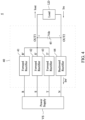
- FIG. 4 is a schematic diagram of a three-phase four-wire power system 4 in accordance with some embodiments of the present disclosure.
- the three-phase four-wire power system 4 includes a power supply VS, an electronic transformer 40 and a load LD.
- the electronic transformer 40 is coupled between the power supply VS and the load LD, and is configured to receive the first phase power source R, the second phase power source S and he third phase power source T from the power supply VS and then to supply power to the load LD by preforming a rectifying transformation on the first phase power source R, the second phase power source S and the third phase power source T as well as being stored and filtered by the capacitor.
- the electronic transformer 40 includes a first forward rectifier 41, a second forward rectifier 42, a third forward rectifier 43, a backward rectifier 44 and a capacitor 45.
- the first forward rectifier 41 is coupled between the first phase power R of the power supply VS and the first output terminal OUT1;
- the second forward rectifier 42 is coupled between the second phase power S of the power supply VS and the first output terminal OUT1;
- the third forward rectifier 43 is coupled between the third phase power T of the power supply VS and the first output terminal OUT1;
- the backward rectifier 44 is coupled between the neutral line N of the power supply VS and the second output terminal OUT2.
- the capacitor 45 is connected between the first output terminal OUT1 and the second output terminal OUT2.
- the second output terminal OUT2 is grounded.
- the first forward rectifier 41, the second forward rectifier 42 and the third forward rectifier 43 are configured to perform half-wave rectification respectively on the first phase power source R, the second phase power source S and the third phase power source T to generate a rectified first phase power source R', a rectified second phase power source S' and a rectified third phase power source T', and the rectified first phase power source R', the rectified second phase power source S' and the rectified third phase power source T' are superposed at the first output terminal OUT1.
- the capacitor 45 is used to smoothen (i.e. filter) the superposed power at the first output terminal OUT1 as the output voltage Vdc that is provided to the load LD.
- the current distribution is balanced because the first forward rectifier 41, the second forward rectifier 42 and the third forward rectifier 43 perform half-wave rectifications respectively on the first phase power source R, the second phase power source S and the third phase power source T.
- the electronic transformer 40 and the three-phase four-wire power system 4 of the present disclosure solves the problems of specific elements being damaged in a short time due to more frequent high current (i.e. unbalanced current distribution).
- the backward rectifier 44 is configured to perform half-wave rectification on the return current Ire to generate the rectified return current Ire', and transmits the rectified return current Ire' back to the power supply VS through the neutral line N.
- the half-wave rectification is performed on the first phase power source R, the second phase power source S and the third phase power source T respectively through the first forward rectifier 41, the second forward rectifier 42 and the third forward rectifier 43, and the rectified first phase power source R', the rectified second phase power source S' and the rectified third phase power source T' are superposed at the first output terminal OUT1, and then the superposed voltage at the first output terminal OUT1 is smoothened (i.e. filtered) through the capacitor 45 as the output voltage Vdc provided to the load LD. Thereafter, the backward rectifier 44 performs half-wave rectification on the return current Ire generated by the load LD, and returns the rectified return current Ire' to the power supply VS through the neutral line N.
- the three-phase power sources R, S, T generated by the power supply VS and rectified respectively through the three forward rectifiers 41, 42, 43 of the electronic transformer 40 are aggregated via the first output terminal OUT1 to form the output current lout that flows into the load LD; thereafter, the return current Ire generated by the load LD and rectified by the backward rectifier 44 of the electronic transformer 40 returns to the power supply VS through the neutral line N.
- a complete current loop is formed between the power supply VS, the electronic transformer 40 and the load LD, and the operations on the forward output current lout and the backward return current Ire are symmetrical and balanced, thereby improving the operational efficiency of the three-phase four-wire power system 4.
- FIG. 5 is a schematic diagram of an electronic transformer 50 in accordance with some embodiments of the present disclosure.
- the electronic transformer 50 is applicable to the three-phase four-wire power system 4 in FIG. 4 in replace of the electronic transformer 40.
- the electronic transformer 50 includes a first forward rectifier 51, a second forward rectifier 52, a third forward rectifier 53, a backward rectifier 54 and a capacitor 55.
- the first forward rectifier 51 includes diodes D1, D2;
- the second forward rectifier 52 includes diodes D3, D4;
- the third forward rectifier 53 includes diodes D5, D6;
- the backward rectifier 54 includes diodesD7, D8.
- each of the rectifiers 51, 52, 53, 54 includes two diodes that are connected in parallel (e.g., in the rectifier 51, the diodes D1, D2 are connected in parallel).
- the cathode of each of the diodes D1, D2 is coupled to the first phase power source R; in the first forward rectifier 51, the cathode of each of the diodes D3, D4 is coupled to the second phase power source S; in the third forward rectifier 53, the cathode of each of the diodes D5, D6 is coupled to the third phase power source T; and the anode of each of the diodes D1, D2, D3, D4, D5, D6 in the first forward rectifier 51, the second forward rectifier 52 and the third forward rectifier 53 is coupled to the first output terminal OUT1.
- the anode of each of the diodes D7, D8 in the backward rectifier 54 is coupled to the neutral line N, and the cathode of each of the diodes D7, D8 in the backward rectifier 54 is coupled to the second output terminal OUT2.
- the capacitor 55 is connected between the first output terminal OUT1 and the second output terminal OUT2.
- DK are all I_D, and the resistivity of each of the diodes D1, D2, ... , DK is R_D.
- the total power P_TOTAL is in reverse proportion to the number of diodes K (because the total current remains unchanged). That is, the overall power loss of the rectifier is reduced as the number of diodes K connected in parallel increases.
- Table 1 Number of Diodes K Diode Current 1 1.00*I_TOTAL 2 0.50*I_TOTAL 3 0.33*I_TOTAL 4 0.25*I_TOTAL 5 0.20*I_TOTAL 6 0.17*I_TOTAL
- the two currents respectively corresponding to the number K of 5 and 6 differ by 3%, and the degree of current drop is already insignificant.
- the number of diodes K connected in parallel in each of the rectifiers 51, 52, 53, 54 may be 2 to 5.
- the electronic transformer 40 shown in FIG. 4 has less electrical elements disposed therein for saving the layout area.
- each of the diodes D1, D2, D3, D4, D5, D6, D7, D8 is a PN junction diode or a fast recovery diode.
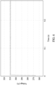
- FIG. 6 is a waveform diagram of the output voltage Vdc of the electronic transformer 50 shown in FIG. 5 .
- selecting a suitable energy storing and filtering capacitor 55 obtains a relatively stable output voltage in comparison with the conventional electronic transformer with two-stage rectification and has advantages.
- FIG. 7 is a waveform diagram of the output current lout of the electronic transformer 50 shown in FIG. 5 , in which currents I71, I72, I73 are the currents respectively outputted by the forward rectifiers 51, 52, 53.
- the currents I71, I72, I73 are aggregated at the first output terminal OUT1 to form the output current lout of the electronic transformer 50.
- a half-wave rectification is performed on the three-phase power sources R, S, T balancedly passing through the forward rectifiers 51, 52, 53, and therefore the currents I71, I72, I73 with balanced distribution can be generated.
- the electronic transformer 50 of the present disclosure solves the problem of specific elements being damaged in a short time due to more frequent high current (i.e. unbalanced current distribution).
- FIG. 8 is a temperature change diagram of the electronic transformer 50 shown in FIG. 5 in 100% load and 150% load operating conditions, in which curves 81, 82 respectively correspond to temperature changes of 100% load and 150% load.
- the temperature of the electronic transformer 50 can be kept in a specific range (e.g. 71 to 77 °C) rather than gradually increasing with time.
- the temperature of the electronic transformer 50 can be kept in a specific range (e.g. 78 to 84 °C) rather than gradually increasing with time. Therefore, the electronic transformer 50 of the present disclosure has the advantage of stable and time-invariant temperature.
- Table 2 Test Condition Output Voltage Highest Temperature Environmental Temperature 100% Load 310 V 81 °C 55 °C 150% Load 310 V 86 °C 55 °C
- FIG. 9 is a schematic diagram of an electronic transformer 90 in accordance with some embodiments of the present disclosure.
- the electronic transformer 90 is applicable to the three-phase four-wire power system 4 in FIG. 4 in replace of the electronic transformer 40.
- the electronic transformer 90 includes a first forward rectifier 91, a second forward rectifier 92, a third forward rectifier 93, a backward rectifier 94 and a capacitor 95.
- the first forward rectifier 91 includes a diode D91;
- the second forward rectifier 92 includes a diode D92;
- the third forward rectifier 93 includes a diode D93; and the backward rectifier 94 includes diodes D94, D95, D96.
- the ratio of the number of diodes in each forward rectifier to the number of diodes in the backward rectifier is 1:3. That is, each of the first forward rectifier, the second forward rectifier and the third forward rectifier includes K diodes that are connected in parallel, and the reverse rectifier includes three groups of K diodes that are connected in parallel.
- the forward rectifier 91/92/93 includes one diode D91/D92/D93
- the backward rectifier 94 includes three diodes D94, D95, D96, and thus the ratio of the number of diodes in the forward rectifier 91/92/93 to the number of diodes in the backward rectifier 94 is 1:3.
- the number of diodes in the three forward rectifiers 91, 92, 93 is identical to the number of diodes in the backward rectifier 94 (i.e. the three backward biased diodes D94, D95, D96).
- the average current through each of the three forward biased diodes D94, D92, D96 is (1/3)*!out
- the average current through each of the three backward diodes D94, D95, D96 is (1/3)*Ire. Therefore, the output current lout is balancedly distributed to the three forward biased diodes D94, D95, D96, and the return current Ire is balancedly distributed to the three backward biased diodes D94, D95, D96, and as such the problem of specific elements being damaged in a short time due to more frequent high current (i.e. unbalanced current distribution), so as to let the operating temperature of the electronic transformer 90 more stable.
- each diode decreases as the number of diodes K connected in parallel increases, such that the loss of each diode is reduced.
- the number K of diodes in parallel connection is 2, then each of the forward rectifiers 91, 92, 93 includes two diodes in parallel connection, and the backward rectifier 94 includes six diodes in parallel connection, and so on.
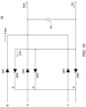
- FIG. 10 is a schematic diagram of an electronic transformer 99 in accordance with some embodiments of the present disclosure.
- the electronic transformer 99 and 90 include the same elements as well as the same connection relationship between elements.
- the difference between the electronic transformers 99 and 90 is that, in the electronic transformers 99, the diodes D91, D92 and D93 are respectively adjacent to the diodes D94, D95 and D96.
- the amplitudes of the forward current (1/3)*lout and the backward current (1/3)*Ire are identical, the directions of the forward current (1/3)*lout and the backward current (1/3)*Ire are opposite, and a differential pair is formed when a forward biased diode is disposed adjacent to a backward biased diode and its circuit. As such, the energy transmission efficiency of the three-phase power sources can be improved.
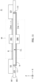
- FIG. 11 is a layout diagram of the electronic transformer 99 and the three-phase four-wire power system 11 shown in FIG. 10 .
- the three-phase four-wire power system 11 includes a circuit board 110 formed in the XY plane; the circuit board 110 includes a first surface SF1 and a second surface SF2.
- a first through via 111 is formed in the circuit board 110 and extends in the Z direction for connecting the power supply VS and the neutral line N.
- a second through via 112 is formed in the circuit board 110 and extends in the Z direction, and is configured to connect the load L and the neutral line N.
- a connector may be disposed on the circuit board 110 to connect the power supply VS, and another connector may be disposed on the circuit board 110 to connect the load LD, and thus the power supply VS and the load LD may be external devices.
- the backward current (1/3)*Ire generated by the load LD is provided to the backward diode D94, and then returns to the power supply VS through the neutral line N.
- a complete current loop CL is formed between the power supply VS, the electronic transformer 99 and the load LD, and the operations of the forward output current and the backward return current are symmetrical and balanced, thereby improving the operational efficiency of the three-phase four-wire power system 11.
- the projections of the live lines for transmitting the first-phase power source, the second-phase power source and the third-phase power source and the forward biased diodes (including the diodes D91, D92, D93) on the first surface SF1 and the projections of the neutral line and the diodes (including the diodes D94, D95, D96) on the second surface SF2 are staggered in the XY plane.
- the area of the current loop CL is approximately the thickness of the circuit board 110 in the Z direction and the line length of neutral line N (or the live lines) along the X direction, such that the area of current loop CL is approximately the minimum value for minimizing the electromagnetic radiation (i.e. energy consumption) generated by the current loop CL.
- the circuit board 110 is a multilayer board (e.g. with four, six or more layers)
- at least one of the live lines for transmitting the three-phase power sources R, S, T and the neutral line N may be formed in the internal layers of the circuit board 110, so as to further reduce the area of the current loop CL and achieves electromagnetic shielding by the surface layer of the circuit board 110 for minimizing the electromagnetic radiation (i.e. energy consumption) generated by the current loop CL.
- the electronic transformer and the three-phase four-wire power supply system thereof perform half-wave rectification respectively on the three-phase power sources through three forward rectifiers to generate an output current with balanced distribution at the first output end. Therefore, the present disclosure solves the problem of specific elements being damaged in a short time due to more frequent high current (i.e. unbalanced current distribution).
- the return current generated by the load returns to the power supply through the neutral line, such that a complete current loop is formed between the power supply, the electronic transformer and the load, and the operations of the forward output current and the backward return current are symmetrical and balanced, thereby improving the operational efficiency of the three-phase four-wire power supply system.
- the electronic transformer and the three-phase four-wire power supply system thereof according to the present disclosure have the following advantages: (1) stable output voltage; (2) output current with balanced distribution; (3) simplified circuit design as well as less layout area and cost; and (4) stable and time-invariant operating temperature.
Landscapes
- Engineering & Computer Science (AREA)
- Power Engineering (AREA)
- Physics & Mathematics (AREA)
- Electromagnetism (AREA)
- Rectifiers (AREA)
- Ac-Ac Conversion (AREA)
Abstract
An electronic transformer includes a first forward rectifier, a second forward rectifier, a third forward rectifier and a backward rectifier. The first forward rectifier is coupled between a first-phase power and a first output terminal. The second forward rectifier is coupled between a second-phase power and the first output terminal. The third forward rectifier is coupled between a third-phase power and the first output terminal. The backward rectifier is coupled between a neutral line and a second output terminal. The first forward rectifier, the second forward rectifier, and the third forward rectifier are configured to half-wave rectify the first-phase power, the second-phase power, and the third-phase power to generate rectified first-phase to third-phase power sources, and superimpose the rectified first-phase to third-phase power sources on the first output end to serve as an output voltage of the electronic transformer.
Description
- The present disclosure relates to an electronic transformer, and more particularly to an electronic transformer and a three-phase four-wire power system thereof.
- Electronic transformers or coil transformers are devices that combine power electronic conversion technology and high-frequency electric energy conversion technology based on the principle of electromagnetic induction to realize electric energy transformation from one electric characteristic into another one. However, as to the aspect of transformation from three-phase alternating current (AC) voltages to a direct current (DC) voltage, conventional coil transformers have the drawbacks of high heat consumption, high power consumption, hard installation, low efficiency and inconvenient transportation. In view of this, the industry is now working on development of a miniaturized electronic transformer in replace of conventional coil transformers.
- One aspect of the present disclosure directs to an electronic transformer which includes a first forward rectifier, a second forward rectifier, a third forward rectifier and a backward rectifier. The first forward rectifier is coupled between a first-phase power source and a first output terminal; the second forward rectifier is coupled between a second-phase power source and the first output terminal; the third forward rectifier is coupled between a third-phase power source and the first output terminal; and the backward rectifier is coupled between a neutral line and a second output terminal. The first forward rectifier, the second forward rectifier and the third forward rectifier are configured to perform half-wave rectification on the first-phase power source, the second-phase power source and the third-phase power source to generate a rectified first-phase power source, a rectified second-phase power source and a rectified third-phase power source, and to superpose the rectified first-phase power source, the rectified second-phase power source and the rectified third-phase power source at the first output terminal as an output voltage of the electronic transformer.
- Another aspect of the present disclosure directs to a three-phase four-wire power system which includes a power supply and a load as well as the aforementioned electronic transformer. The power supply includes a neutral line, and is configured to provide a first-phase power source, a second-phase power source and a third-phase power source. The electronic transformer is coupled between the power supply and the load, and is configured to convert the first-phase power source, the second-phase power source and the third-phase power source into an output voltage to the load.
- The electronic transformer and the three-phase four-wire power supply system thereof according to the present disclosure perform half-wave rectification on the three-phase power sources respectively through three forward rectifiers to generate an output current with balanced distribution at the first output end. In addition, after being rectified by the backward rectifier, the return current generated by the load returns to the power supply through the neutral line, such that a complete current loop is formed between the power supply, the electronic transformer and the load, and the operations of the forward output current and the backward return current are symmetrical and balanced, thereby improving the operational efficiency of the three-phase four-wire power supply system. Therefore, the present disclosure solves the problem that certain components are damaged in a short time due to unbalanced current distribution. Moreover, the present disclosure does not need to be configured as a three-phase three-wire structure for the use of back-end products, and the design of the electronic transformer of the present disclosure is simpler than that of a conventional electronic transformer. The electronic transformer and the three-phase four-wire power supply system thereof according to the present disclosure have the following advantages: (1) stable output voltage; (2) output current with balanced distribution; (3) simplified circuit design as well as less layout area and cost; and (4) stable and time-invariant operating temperature.
- The foregoing aspects and many of the accompanying advantages of this invention will become more readily appreciated as the same becomes better understood by reference to the following detailed description, when taken in conjunction with the accompanying drawings.
-
FIG. 1 is a schematic diagram of a three-phase four-wire power system. -
FIG. 2 is a voltage waveform diagram of the three-phase power sources and the three nodes of the electronic transformer inFIG. 1 . -
FIG. 3 is a current waveform diagram of the first output terminal of the electronic transformer inFIG. 1 . -
FIG. 4 is a schematic diagram of a three-phase four-wire power system in accordance with some embodiments of the present disclosure. -
FIG. 5 is a schematic diagram of an electronic transformer in accordance with some embodiments of the present disclosure. -
FIG. 6 is a waveform diagram of the output voltage of the electronic transformer shown inFIG. 5 . -
FIG. 7 is a waveform diagram of the output current of the electronic transformer shown inFIG. 5 . -
FIG. 8 is a temperature change diagram of the electronic transformer shown inFIG. 5 in 100% load and 150% load operating conditions. -
FIG. 9 is a schematic diagram of an electronic transformer in accordance with some embodiments of the present disclosure. -
FIG. 10 is a schematic diagram of an electronic transformer in accordance with some embodiments of the present disclosure. -
FIG. 11 is a layout diagram of the electronic transformer and the three-phase four-wire power system shown inFIG. 10 . - The detailed explanation of the invention is described as following. The described preferred embodiments are presented for purposes of illustrations and description, and they are not intended to limit the scope of the invention.
-
FIG. 1 is a schematic diagram of a three-phase four-wire power system (hereinafter abbreviated "system") 1. Thesystem 1 includes a power supply VS, anelectronic transformer 10 and a load LD. The power supply VS transmits three-phase power sources R, S, T to theelectronic transformer 10 respectively through three live lines. Theelectronic transformer 10 performs rectification on the first phase power source R, the second phase power source S and the third phase power source T respectively through three bridge rectifiers for supplying power to the load LD. Theelectronic transformer 10 includes a front-end bridge transforming circuit and back-end six-phase inverters. In operation, the bridge transforming circuit is configured to perform rectifying transformation on the first phase power source R, the second phase power source S and the third phase power source T before the node L1, L2, L3; the six-phase inverters perform a secondary rectification after the nodes L1, L2, L3; the capacitor 15 is connected between the first output terminal OUT1 and the second output terminal OUT2, and is used to store energy and filter the rectified voltage, so as to provide the smoothened (i.e. filtered) voltage to the load LD. - However, in the
electronic transformer 10, the design of the bridge transforming circuit results in unbalanced voltage distribution. Specifically, the two bridge rectifiers which respectively receive the first phase power source R and the second phase power source S are connected to the node L1; the bridge rectifier which receives the third phase power source T is connected to the node L2; and the neutral line N is directly connected to the node L3. Therefore, the transformed voltages respectively from the first phase power source R and the second phase power source S are simultaneously transmitted to the six-phase inverters through the node L1; the transformed voltage from the third phase power source T is transmitted to the six-phase inverters through the node L2; and the neutral line N is connected to the six-phase inverters through the node L3. However, the power supply VS does not provide any energy to the neutral line N. Unbalanced currents would be induced if the unbalanced voltages are transmitted to the six-phase inverters for rectification. With the operation time of theelectronic transformer 10 continuously elapses, specific elements (e.g., the diode connected to the node L1) are damaged faster than the other elements because of heat due to more frequent high current. In addition, in the power system, the lines of the three-phase power sources R, S, T may not be adapted in order, and thus the elements heated due to high current are not fixed, resulting in difficulty of product troubleshooting in the future. -
FIG. 2 is a voltage waveform diagram of the three-phase power sources R, S, T and the nodes L1, L2, L3 of theelectronic transformer 10 inFIG. 1 . The three-phase power sources R, S, T are alternating-current voltages with the same amplitude and frequency as well as phases displaced with respect to each other by 120 degrees; the line voltage of each may be such as 380 volts, and the phase voltage of each may be such as 220 volts, but the present disclosure is not limited thereto. The transformed voltages respectively from the first phase power source R and the second phase power source S are simultaneously transmitted through the node L1, and thus the node L1 bears a doubled current stress. The transformed voltage from the third phase power source T is transmitted through the node L2, and thus the node L2 bears a normal current stress. Moreover, the power supply VS does not provide energy to the neutral line N, and thus the voltage of the node L3 originates from the backward voltage of the load LD. As can be seen fromFIG. 2 , the voltages and the currents distributed to the nodes L1, L2, L3 are unbalanced. -
FIG. 3 is a current waveform diagram of the first output terminal OUT1 of theelectronic transformer 10 inFIG. 1 . The currents I31, I32, I33 are the currents flowing to the first output terminal OUT1 respectively from the nodes L1, L2, L3 through the diodes. At the first output terminal OUT1, the current I31 is generated according to the transformed voltages of the first phase power source R and the second phase power source S, and thus has a sawtooth waveform of two phases; the current I32 is generated according to the transformed voltage of the third phase power source T, and thus has a sawtooth waveform of one phase; the current I33 is generated according to the transformed voltage of the neutral line N, and thus keeps at zero current without having any sawtooth waveform with one phase. As can been from the above, theelectronic transformer 10 has the problem of unbalanced currents during operation. In a condition in which theelectronic transformer 10 is used for a long time, specific elements for generating the current I31 are damaged faster than the other elements because of heat and rising temperature due to more frequent high current. In addition, more electrical components are needed to be arranged for theelectronic transformer 10 inFIG. 1 , and thus more layout area is needed. -
FIG. 4 is a schematic diagram of a three-phase four-wire power system 4 in accordance with some embodiments of the present disclosure. The three-phase four-wire power system 4 includes a power supply VS, anelectronic transformer 40 and a load LD. Theelectronic transformer 40 is coupled between the power supply VS and the load LD, and is configured to receive the first phase power source R, the second phase power source S and he third phase power source T from the power supply VS and then to supply power to the load LD by preforming a rectifying transformation on the first phase power source R, the second phase power source S and the third phase power source T as well as being stored and filtered by the capacitor. - Structurally, the
electronic transformer 40 includes a firstforward rectifier 41, a secondforward rectifier 42, a thirdforward rectifier 43, abackward rectifier 44 and acapacitor 45. The firstforward rectifier 41 is coupled between the first phase power R of the power supply VS and the first output terminal OUT1; the secondforward rectifier 42 is coupled between the second phase power S of the power supply VS and the first output terminal OUT1; the thirdforward rectifier 43 is coupled between the third phase power T of the power supply VS and the first output terminal OUT1; and thebackward rectifier 44 is coupled between the neutral line N of the power supply VS and the second output terminal OUT2. Thecapacitor 45 is connected between the first output terminal OUT1 and the second output terminal OUT2. The second output terminal OUT2 is grounded. - In operation, the first
forward rectifier 41, the secondforward rectifier 42 and the thirdforward rectifier 43 are configured to perform half-wave rectification respectively on the first phase power source R, the second phase power source S and the third phase power source T to generate a rectified first phase power source R', a rectified second phase power source S' and a rectified third phase power source T', and the rectified first phase power source R', the rectified second phase power source S' and the rectified third phase power source T' are superposed at the first output terminal OUT1. Thecapacitor 45 is used to smoothen (i.e. filter) the superposed power at the first output terminal OUT1 as the output voltage Vdc that is provided to the load LD. The current distribution is balanced because the firstforward rectifier 41, the secondforward rectifier 42 and the thirdforward rectifier 43 perform half-wave rectifications respectively on the first phase power source R, the second phase power source S and the third phase power source T. As a result, theelectronic transformer 40 and the three-phase four-wire power system 4 of the present disclosure solves the problems of specific elements being damaged in a short time due to more frequent high current (i.e. unbalanced current distribution). - Then, after the load LD receives the output voltage Vdc, the return current Ire generated by the load LD further passes through the second output terminal OUT2 to flow into the
electronic transformer 40. Thebackward rectifier 44 is configured to perform half-wave rectification on the return current Ire to generate the rectified return current Ire', and transmits the rectified return current Ire' back to the power supply VS through the neutral line N. - Simply speaking, in the
electronic transformer 40, the half-wave rectification is performed on the first phase power source R, the second phase power source S and the third phase power source T respectively through the firstforward rectifier 41, the secondforward rectifier 42 and the thirdforward rectifier 43, and the rectified first phase power source R', the rectified second phase power source S' and the rectified third phase power source T' are superposed at the first output terminal OUT1, and then the superposed voltage at the first output terminal OUT1 is smoothened (i.e. filtered) through thecapacitor 45 as the output voltage Vdc provided to the load LD. Thereafter, thebackward rectifier 44 performs half-wave rectification on the return current Ire generated by the load LD, and returns the rectified return current Ire' to the power supply VS through the neutral line N. - From another point of view, the three-phase power sources R, S, T generated by the power supply VS and rectified respectively through the three
forward rectifiers electronic transformer 40 are aggregated via the first output terminal OUT1 to form the output current lout that flows into the load LD; thereafter, the return current Ire generated by the load LD and rectified by thebackward rectifier 44 of theelectronic transformer 40 returns to the power supply VS through the neutral line N. As such, a complete current loop is formed between the power supply VS, theelectronic transformer 40 and the load LD, and the operations on the forward output current lout and the backward return current Ire are symmetrical and balanced, thereby improving the operational efficiency of the three-phase four-wire power system 4. -
FIG. 5 is a schematic diagram of anelectronic transformer 50 in accordance with some embodiments of the present disclosure. Theelectronic transformer 50 is applicable to the three-phase four-wire power system 4 inFIG. 4 in replace of theelectronic transformer 40. Structurally, theelectronic transformer 50 includes a firstforward rectifier 51, a secondforward rectifier 52, a thirdforward rectifier 53, abackward rectifier 54 and acapacitor 55. The firstforward rectifier 51 includes diodes D1, D2; the secondforward rectifier 52 includes diodes D3, D4; the thirdforward rectifier 53 includes diodes D5, D6; and thebackward rectifier 54 includes diodesD7, D8. - In the embodiment, each of the
rectifiers rectifier 51, the diodes D1, D2 are connected in parallel). In the firstforward rectifier 51, the cathode of each of the diodes D1, D2 is coupled to the first phase power source R; in the firstforward rectifier 51, the cathode of each of the diodes D3, D4 is coupled to the second phase power source S; in the thirdforward rectifier 53, the cathode of each of the diodes D5, D6 is coupled to the third phase power source T; and the anode of each of the diodes D1, D2, D3, D4, D5, D6 in the firstforward rectifier 51, the secondforward rectifier 52 and the thirdforward rectifier 53 is coupled to the first output terminal OUT1. The anode of each of the diodes D7, D8 in thebackward rectifier 54 is coupled to the neutral line N, and the cathode of each of the diodes D7, D8 in thebackward rectifier 54 is coupled to the second output terminal OUT2. Thecapacitor 55 is connected between the first output terminal OUT1 and the second output terminal OUT2. The operating method of theelectronic transformer 50 is similar to that of theelectronic transformer 40, and thus the description thereof is not repeated herein. - It is noted that each of the
rectifiers 


- The current through each of the K diodes connected in parallel are listed in Table 1 shown below.
Table 1 Number of Diodes K Diode Current 1 1.00*I_TOTAL 2 0.50*I_TOTAL 3 0.33* I_TOTAL 4 0.25*I_TOTAL 5 0.20*I_TOTAL 6 0.17*I_TOTAL - As can be seen from Table 1, the two currents respectively corresponding to the number K of 5 and 6 differ by 3%, and the degree of current drop is already insignificant. By comprehensively considering the power consumption and the layout area of the
electronic transformer 50, in some embodiments, the number of diodes K connected in parallel in each of therectifiers electronic transformer 10 shown inFIG. 1 in which more electrical components (i.e. three bridge rectifiers and six-phase inverters) are disposed, theelectronic transformer 40 shown inFIG. 4 has less electrical elements disposed therein for saving the layout area. - In one embodiment, each of the diodes D1, D2, D3, D4, D5, D6, D7, D8 is a PN junction diode or a fast recovery diode.
-
FIG. 6 is a waveform diagram of the output voltage Vdc of theelectronic transformer 50 shown inFIG. 5 . With the structure of balanced voltages and currents, selecting a suitable energy storing andfiltering capacitor 55 obtains a relatively stable output voltage in comparison with the conventional electronic transformer with two-stage rectification and has advantages. -
FIG. 7 is a waveform diagram of the output current lout of theelectronic transformer 50 shown inFIG. 5 , in which currents I71, I72, I73 are the currents respectively outputted by theforward rectifiers electronic transformer 50. As can be seen fromFIG. 7 , a half-wave rectification is performed on the three-phase power sources R, S, T balancedly passing through theforward rectifiers electronic transformer 50 of the present disclosure solves the problem of specific elements being damaged in a short time due to more frequent high current (i.e. unbalanced current distribution). -
FIG. 8 is a temperature change diagram of theelectronic transformer 50 shown inFIG. 5 in 100% load and 150% load operating conditions, in which curves 81, 82 respectively correspond to temperature changes of 100% load and 150% load. As can be seen fromFIG. 8 , except the moment in the early stage of powering at which the temperature rises to the maximum temperature, with the operation time continuously elapses, in a full-load (100% load) operating condition, the temperature of theelectronic transformer 50 can be kept in a specific range (e.g. 71 to 77 °C) rather than gradually increasing with time. In addition, in an overload (150% load) operating condition, the temperature of theelectronic transformer 50 can be kept in a specific range (e.g. 78 to 84 °C) rather than gradually increasing with time. Therefore, theelectronic transformer 50 of the present disclosure has the advantage of stable and time-invariant temperature. - The test conditions and the results of the
electronic transformer 50 are summarized in Table 2 shown below.Table 2 Test Condition Output Voltage Highest Temperature Environmental Temperature 100% Load 310 V 81 ° C 55 °C 150% Load 310 V 86 ° C 55 °C -
FIG. 9 is a schematic diagram of anelectronic transformer 90 in accordance with some embodiments of the present disclosure. Theelectronic transformer 90 is applicable to the three-phase four-wire power system 4 inFIG. 4 in replace of theelectronic transformer 40. Structurally, theelectronic transformer 90 includes a firstforward rectifier 91, a secondforward rectifier 92, a thirdforward rectifier 93, abackward rectifier 94 and acapacitor 95. The firstforward rectifier 91 includes a diode D91; the secondforward rectifier 92 includes a diode D92; the thirdforward rectifier 93 includes a diode D93; and thebackward rectifier 94 includes diodes D94, D95, D96. - In some embodiments, the ratio of the number of diodes in each forward rectifier to the number of diodes in the backward rectifier is 1:3. That is, each of the first forward rectifier, the second forward rectifier and the third forward rectifier includes K diodes that are connected in parallel, and the reverse rectifier includes three groups of K diodes that are connected in parallel. For illustration, in this embodiment, the
forward rectifier 91/92/93 includes one diode D91/D92/D93, and thebackward rectifier 94 includes three diodes D94, D95, D96, and thus the ratio of the number of diodes in theforward rectifier 91/92/93 to the number of diodes in thebackward rectifier 94 is 1:3. From another point of view, the number of diodes in the threeforward rectifiers - In the configuration of
FIG. 9 , in the long term, the average current through each of the three forward biased diodes D94, D92, D96 is (1/3)*!out, and the average current through each of the three backward diodes D94, D95, D96 is (1/3)*Ire. Therefore, the output current lout is balancedly distributed to the three forward biased diodes D94, D95, D96, and the return current Ire is balancedly distributed to the three backward biased diodes D94, D95, D96, and as such the problem of specific elements being damaged in a short time due to more frequent high current (i.e. unbalanced current distribution), so as to let the operating temperature of theelectronic transformer 90 more stable. - As can be seen from the embodiment of
FIG. 5 , the current of each diode decreases as the number of diodes K connected in parallel increases, such that the loss of each diode is reduced. Thus, in some embodiments, if the number K of diodes in parallel connection is 2, then each of theforward rectifiers backward rectifier 94 includes six diodes in parallel connection, and so on. -
FIG. 10 is a schematic diagram of anelectronic transformer 99 in accordance with some embodiments of the present disclosure. Theelectronic transformer electronic transformers electronic transformers 99, the diodes D91, D92 and D93 are respectively adjacent to the diodes D94, D95 and D96. For each of the forward biased and backward biased diodes, the amplitudes of the forward current (1/3)*lout and the backward current (1/3)*Ire are identical, the directions of the forward current (1/3)*lout and the backward current (1/3)*Ire are opposite, and a differential pair is formed when a forward biased diode is disposed adjacent to a backward biased diode and its circuit. As such, the energy transmission efficiency of the three-phase power sources can be improved. -
FIG. 11 is a layout diagram of theelectronic transformer 99 and the three-phase four-wire power system 11 shown inFIG. 10 . The three-phase four-wire power system 11 includes acircuit board 110 formed in the XY plane; thecircuit board 110 includes a first surface SF1 and a second surface SF2. Structurally, the power supply VS, the diode D91 in the forward rectifier 91 (the diodes D92, D93 in theforward rectifiers circuit board 110 and extends in the Z direction for connecting the power supply VS and the neutral line N. A second through via 112 is formed in thecircuit board 110 and extends in the Z direction, and is configured to connect the load L and the neutral line N. In one embodiment, a connector may be disposed on thecircuit board 110 to connect the power supply VS, and another connector may be disposed on thecircuit board 110 to connect the load LD, and thus the power supply VS and the load LD may be external devices. - In the configuration of
FIG. 11 , after the forward current (1/3)*lout generated by the forward biased diode D91 is provided to the load LD through the live line, the backward current (1/3)*Ire generated by the load LD is provided to the backward diode D94, and then returns to the power supply VS through the neutral line N. As such, a complete current loop CL is formed between the power supply VS, theelectronic transformer 99 and the load LD, and the operations of the forward output current and the backward return current are symmetrical and balanced, thereby improving the operational efficiency of the three-phase four-wire power system 11. - In one embodiment, the projections of the live lines for transmitting the first-phase power source, the second-phase power source and the third-phase power source and the forward biased diodes (including the diodes D91, D92, D93) on the first surface SF1 and the projections of the neutral line and the diodes (including the diodes D94, D95, D96) on the second surface SF2 are staggered in the XY plane. In this structure, the area of the current loop CL is approximately the thickness of the
circuit board 110 in the Z direction and the line length of neutral line N (or the live lines) along the X direction, such that the area of current loop CL is approximately the minimum value for minimizing the electromagnetic radiation (i.e. energy consumption) generated by the current loop CL. In another embodiment, if thecircuit board 110 is a multilayer board (e.g. with four, six or more layers), then at least one of the live lines for transmitting the three-phase power sources R, S, T and the neutral line N may be formed in the internal layers of thecircuit board 110, so as to further reduce the area of the current loop CL and achieves electromagnetic shielding by the surface layer of thecircuit board 110 for minimizing the electromagnetic radiation (i.e. energy consumption) generated by the current loop CL. - In summary, the electronic transformer and the three-phase four-wire power supply system thereof according to the present disclosure perform half-wave rectification respectively on the three-phase power sources through three forward rectifiers to generate an output current with balanced distribution at the first output end. Therefore, the present disclosure solves the problem of specific elements being damaged in a short time due to more frequent high current (i.e. unbalanced current distribution). In addition, after being rectified by the backward rectifier, the return current generated by the load returns to the power supply through the neutral line, such that a complete current loop is formed between the power supply, the electronic transformer and the load, and the operations of the forward output current and the backward return current are symmetrical and balanced, thereby improving the operational efficiency of the three-phase four-wire power supply system. The electronic transformer and the three-phase four-wire power supply system thereof according to the present disclosure have the following advantages: (1) stable output voltage; (2) output current with balanced distribution; (3) simplified circuit design as well as less layout area and cost; and (4) stable and time-invariant operating temperature.
Claims (15)
- An electronic transformer (40), characterized by comprising:a first forward rectifier (41) coupled between a first-phase power source (R) and a first output terminal (OUT1);a second forward rectifier (42) coupled between a second-phase power source (S) and the first output terminal (OUT1);a third forward rectifier (43) coupled between a third-phase power source (T) and the first output terminal (OUT1); anda backward rectifier (44) coupled between a neutral line (N) and a second output terminal (OUT2);wherein the first forward rectifier (41), the second forward rectifier (42) and the third forward rectifier (43) are configured to perform half-wave rectification on the first-phase power source (R), the second-phase power source (S) and the third-phase power source (T) to generate a rectified first-phase power source (R'), a rectified second-phase power source (S') and a rectified third-phase power source (T'), and to superpose the rectified first-phase power source (R'), the rectified second-phase power source (S') and the rectified third-phase power source (T') at the first output terminal (OUT1) as an output voltage (Vdc) of the electronic transformer (40).
- The electronic transformer (40) of claim 1, characterized by further comprising:
a capacitor (45) coupled between the first output terminal (OUT1) and the second output terminal (OUT2) and configured to store energy and filter the output voltage (Vdc). - The electronic transformer (40) of claim 1, characterized in that the output voltage (Vdc) is supplied to a load to generate a return current (Ire) at the second output terminal; and the backward rectifier (44) is configured to perform half-wave rectification on the return current (Ire) to generate a rectified return current (Ire'), and transmits the rectified return current (Ire') to a power supply (VS) through the neutral line (N).
- The electronic transformer (40) of claim 1, characterized in that each of the first forward rectifier (41), the second forward rectifier (41), the third forward rectifier (43) and the backward rectifier (44) includes 2 to 5 diodes that are connected in parallel.
- The electronic transformer (40, 50) of claim 4, characterized in that:
a cathode of each diode (D1-D2) in the first forward rectifier (41, 51) is coupled to the first-phase power source (R), a cathode of each diode (D3-D4) in the second forward rectifier (42, 52) is coupled to the second-phase power source (S), a cathode of each diode (D5, D6) in the third forward rectifier (43, 53) is coupled to the third-phase power source (T), an anode of each diode (D1-D6) in the first forward rectifier (41, 51), the second forward rectifier (42, 52) and the third forward rectifier (43, 53) is coupled to the first output terminal (OUT1), an anode of each diode (D7-D8) in the backward rectifier (44, 54) is coupled to the neutral line (N), and a cathode of each diode (D7-D8) in the backward rectifier (44, 54) is coupled to the second output terminal (OUT2). - The electronic transformer (40) of claim 1, characterized in that a ratio of the number of diodes in each of the first forward rectifier (41), the second forward rectifier (42) and the third forward rectifier (43) to the number of diodes in the backward rectifier (44) is 1:3.
- The electronic transformer (40) of claim 6, characterized in that diodes in the first forward rectifier (41), the second forward rectifier (42) and the third forward rectifier (43) are respectively adjacent to diodes in the backward rectifier (44).
- The electronic transformer (40) of claim 6, characterized in that each of the first forward rectifier (41), the second forward rectifier (42) and the third forward rectifier (43) comprises K diodes that are connected in parallel, and the backward rectifier (44) comprises three groups of K diodes that are connected in parallel, wherein K is an integer of 2 to 5.
- The electronic transformer (40) of claim 8, characterized in that:
a cathode of each diode in the first forward rectifier (41) is coupled to the first-phase power source (R), a cathode of each diode in the second forward rectifier (42) is coupled to the second-phase power source (S), a cathode of each diode in the third forward rectifier (43) is coupled to the third-phase power source (T), an anode of each diode in the first forward rectifier (41), the second forward rectifier (42) and the third forward rectifier (43) is coupled to the first output terminal (OUT1), an anode of each diode in the backward rectifier (44) is coupled to the neutral line (N), and a cathode of each diode in the backward rectifier (44) is coupled to the second output terminal (OUT2). - A three-phase four-wire power system (4), characterized by comprising:a power supply (VS) configured to provide a first-phase power source (R), a second-phase power source (S) and a third-phase power source (T), the power supply (VS) having a neutral line (N);a load (LD); andan electronic transformer (40) coupled between the power supply (VS) and the load (LD), the electronic transformer (40) comprising:a first forward rectifier (41) coupled between the first-phase power source (R) and a first output terminal (OUT1);a second forward rectifier (42) coupled between the second-phase power source (S) and the first output terminal (OUT1);a third forward rectifier (43) coupled between the third-phase power source (T) and the first output terminal (OUT1); anda backward rectifier (44) coupled between the neutral line (N) and a second output terminal (OUT2);wherein the first forward rectifier (41), the second forward rectifier (42) and the third forward rectifier (43) are configured to perform half-wave rectification on the first-phase power source (R), the second-phase power source (S) and the third-phase power source (T) to generate a rectified first-phase power source (R'), a rectified second-phase power source (S') and a rectified third-phase power source (T'), and to superpose the rectified first-phase power source (R'), the rectified second-phase power source (S') and the rectified third-phase power source (T') at the first output terminal (OUT1) as an output voltage (Vdc) of the electronic transformer (40).
- The three-phase four-wire power system (4) of claim 10, characterized in that the electronic transformer (40) further comprises:
a capacitor (45) coupled between the first output terminal (OUT1) and the second output terminal (OUT2) and configured to store energy and filter the output voltage (Vdc). - The three-phase four-wire power system (4) of claim 10, characterized in that the output voltage (Vdc) is supplied to the load (LD) to generate a return current (Ire) at the second output terminal (OUT2); and the backward rectifier (44) is configured to perform half-wave rectification on the return current (Ire) to generate a rectified return current (Ire'), and transmits the rectified return current (Ire') to the power supply (VS) through the neutral line (N).
- The three-phase four-wire power system (4) of claim 10, characterized in that:each of the first forward rectifier (41), the second forward rectifier (42), the third forward rectifier (43) and the backward rectifier (44) comprises 2 to 5 diodes that are connected in parallel; anda cathode of each diode (D1-D2) in the first forward rectifier (41, 51) is coupled to the first-phase power source (R), a cathode of each diode (D3-D4) in the second forward rectifier (42, 52) is coupled to the second-phase power source (S), a cathode of each diode (D5-D6) in the third forward rectifier (43, 53) is coupled to the third-phase power source (43, 53), an anode of each diode (D1-D6) in the first forward rectifier (41, 51), the second forward rectifier (42, 52) and the third forward rectifier (43, 53) is coupled to the first output terminal (OUT1), an anode of each diode (D7-D8) in the backward rectifier (44, 54) is coupled to the neutral line (N), and a cathode of each diode (D7-D8) in the backward rectifier (44, 54) is coupled to the second output terminal (OUT2).
- The three-phase four-wire power system (4) of claim 10, characterized in that:a ratio of the number of diodes in each of the first forward rectifier (41), the second forward rectifier (42) and the third forward rectifier (43) to the number of diodes in the backward rectifier (44) is 1:3;diodes (D91-D93) in the first forward rectifier (41, 91), the second forward rectifier (42, 92) and the third forward rectifier (43, 93) are respectively adjacent to diodes (D94-D96) in the backward rectifier (44, 94);each of the first forward rectifier (41), the second forward rectifier (42) and the third forward rectifier (43) comprises K diodes that are connected in parallel, and the backward rectifier (44) comprises three groups of K diodes that are connected in parallel, wherein K is an integer of 2 to 5; anda cathode of each diode in the first forward rectifier (41) is coupled to the first-phase power source (R), a cathode of each diode in the second forward rectifier (42) is coupled to the second-phase power source (S), a cathode of each diode in the third forward rectifier (43) is coupled to the third-phase power source (T), an anode of each diode in the first forward rectifier (41), the second forward rectifier (42) and the third forward rectifier (43) is coupled to the first output terminal (OUT1), an anode of each diode in the backward rectifier (44) is coupled to the neutral line (N), and a cathode of each diode in the backward rectifier (44) is coupled to the second output terminal (OUT2).
- The three-phase four-wire power system (4, 11) of claim 14, characterized by further comprising a circuit board (110) that is formed in a plane of a first direction (X) and a second direction (Y), the circuit board (110) comprising:a first surface (SF1) on which the power supply (VS), the diodes of the first forward rectifier (41), the second forward rectifier (42) and the third forward rectifier (43), live lines used for transmitting the first-phase power source (R), the second-phase power source (S) and the third-phase power source (T) and the load (LD) are disposed; anda second surface (SF2) on which diodes in the backward rectifier (44) and the neutral line (N) are disposed,wherein projections of the live lines for transmitting the first-phase power source (R), the second-phase power source (S) and the third-phase power source (T) and diodes in the first forward rectifier (41), the second forward rectifier (42) and the third forward rectifier (43) and projections of the neutral line (N) and the diodes in the backward rectifier (44) are staggered in the plane, and the three-phase four-wire power system (4) further comprises:a first through via (111) disposed in the circuit board (110) and extending in a third direction (Z), the first through via (111) configured to connect the power supply (VS) and the neutral line (N); anda second through via (112) disposed in the circuit board (110) and extending in the third direction (Z), the second through via (112) configured to connect the load (LD) and the neutral line (N).
Applications Claiming Priority (1)
| Application Number | Priority Date | Filing Date | Title |
|---|---|---|---|
| CN202210991062.8A CN117639529A (en) | 2022-08-18 | 2022-08-18 | Electronic transformer and its three-phase four-wire power supply system |
Publications (1)
| Publication Number | Publication Date |
|---|---|
| EP4325710A1 true EP4325710A1 (en) | 2024-02-21 |
Family
ID=84820037
Family Applications (1)
| Application Number | Title | Priority Date | Filing Date |
|---|---|---|---|
| EP23150236.0A Pending EP4325710A1 (en) | 2022-08-18 | 2023-01-04 | Electronic transformer and three-phase four-wire power system thereof |
Country Status (5)
| Country | Link |
|---|---|
| US (1) | US12562652B2 (en) |
| EP (1) | EP4325710A1 (en) |
| JP (1) | JP7772302B2 (en) |
| CN (1) | CN117639529A (en) |
| WO (1) | WO2024037182A1 (en) |
Citations (5)
| Publication number | Priority date | Publication date | Assignee | Title |
|---|---|---|---|---|
| US3081424A (en) * | 1960-01-11 | 1963-03-12 | Ite Circuit Breaker Ltd | Semi-conductor rectifier bridge construction |
| JPS4610331Y1 (en) * | 1965-09-25 | 1971-04-12 | ||
| US4924371A (en) * | 1989-07-10 | 1990-05-08 | General Electric Company | Rectifier circuit provoding compression of the dynamic range of the output voltage |
| CN101369784B (en) * | 2008-06-24 | 2011-02-09 | 何川江 | Electronic servo transformer and servo system |
| CN202602348U (en) * | 2012-05-18 | 2012-12-12 | 徐宁 | Wind and light complementary wind energy generator charging controller |
Family Cites Families (20)
| Publication number | Priority date | Publication date | Assignee | Title |
|---|---|---|---|---|
| JPS4714258Y1 (en) * | 1968-07-23 | 1972-05-23 | ||
| JPS4714258U (en) | 1971-03-19 | 1972-10-19 | ||
| US5051883A (en) * | 1990-07-25 | 1991-09-24 | Cheng Chin Y | Method and an apparatus for full wave rectification of a three-phase signal operating in a wye configuration |
| JPH0731150A (en) | 1993-07-09 | 1995-01-31 | Shindengen Electric Mfg Co Ltd | Switching power supply |
| JPH08228436A (en) | 1995-02-21 | 1996-09-03 | Fuji Electric Co Ltd | Large current rectifier |
| JP2000060130A (en) | 1998-08-18 | 2000-02-25 | Toshiba Corp | DC high voltage generator |
| JP2006180652A (en) | 2004-12-24 | 2006-07-06 | Matsushita Electric Ind Co Ltd | DC power supply |
| CN201409093Y (en) | 2009-01-06 | 2010-02-17 | 青岛四方铁路电气设备有限公司 | Dual-bridge full-wave rectifier cabinet |
| US8664876B2 (en) | 2009-06-29 | 2014-03-04 | Tai-Her Yang | Lighting device with optical pulsation suppression by polyphase-driven electric energy |
| TWI403679B (en) | 2010-04-15 | 2013-08-01 | Delta Electronics Inc | Heating apparatus having plurality of induction coils |
| US20120120697A1 (en) | 2010-11-13 | 2012-05-17 | Cuks, Llc. | Three-phase isolated rectifer with power factor correction |
| CN201976015U (en) | 2011-04-18 | 2011-09-14 | 黄岳胜 | Electronic servo transformer |
| US9712080B2 (en) | 2013-03-14 | 2017-07-18 | Astec International Limited | Reducing phase current imbalances in single phase redundant power supply systems with unbalanced loads |
| JP6361217B2 (en) | 2014-03-26 | 2018-07-25 | ダイキン工業株式会社 | Power converter |
| CN103986345B (en) | 2014-04-30 | 2017-05-03 | 上海汇波智能控制设备有限公司 | Single-phase/three-phase full-voltage power adapter |
| CN104993721A (en) | 2015-06-25 | 2015-10-21 | 西安工程大学 | Three-phase voltage tripling rectifying circuit |
| JP2017112784A (en) | 2015-12-18 | 2017-06-22 | 三菱電機株式会社 | High frequency rectifier circuit |
| CN107748346A (en) | 2017-10-11 | 2018-03-02 | 国网江西省电力公司电力科学研究院 | A kind of high voltage electric energy error detection method under load containing DC component |
| US11601042B2 (en) | 2020-05-14 | 2023-03-07 | Delta Electronics, Inc. | Multi-phase AC/DC converter |
| CN112366962B (en) | 2020-11-03 | 2021-11-09 | 哈尔滨工业大学 | Three-phase three-level rectifier based on three-winding isolation transformer |
-
2022
- 2022-08-18 CN CN202210991062.8A patent/CN117639529A/en active Pending
- 2022-11-15 US US18/055,415 patent/US12562652B2/en active Active
-
2023
- 2023-01-04 EP EP23150236.0A patent/EP4325710A1/en active Pending
- 2023-06-21 WO PCT/CN2023/101967 patent/WO2024037182A1/en not_active Ceased
- 2023-08-08 JP JP2023129303A patent/JP7772302B2/en active Active
Patent Citations (5)
| Publication number | Priority date | Publication date | Assignee | Title |
|---|---|---|---|---|
| US3081424A (en) * | 1960-01-11 | 1963-03-12 | Ite Circuit Breaker Ltd | Semi-conductor rectifier bridge construction |
| JPS4610331Y1 (en) * | 1965-09-25 | 1971-04-12 | ||
| US4924371A (en) * | 1989-07-10 | 1990-05-08 | General Electric Company | Rectifier circuit provoding compression of the dynamic range of the output voltage |
| CN101369784B (en) * | 2008-06-24 | 2011-02-09 | 何川江 | Electronic servo transformer and servo system |
| CN202602348U (en) * | 2012-05-18 | 2012-12-12 | 徐宁 | Wind and light complementary wind energy generator charging controller |
Also Published As
| Publication number | Publication date |
|---|---|
| JP2024028166A (en) | 2024-03-01 |
| US20240063728A1 (en) | 2024-02-22 |
| US12562652B2 (en) | 2026-02-24 |
| JP7772302B2 (en) | 2025-11-18 |
| CN117639529A (en) | 2024-03-01 |
| WO2024037182A1 (en) | 2024-02-22 |
Similar Documents
| Publication | Publication Date | Title |
|---|---|---|
| US9425703B2 (en) | AC/DC converter circuit for common three-phase AC input voltages and method of operating such converter circuit | |
| US6751107B2 (en) | DC power supply device with constant power output level | |
| US4084220A (en) | Power converter | |
| US20090196073A1 (en) | Switching power supply unit | |
| US20140153303A1 (en) | Solar module having a back plane integrated inverter | |
| US20140117769A1 (en) | Master slave architecture for distributed dc to ac power conversion | |
| US20150008748A1 (en) | Power Converter Circuit, Power Supply System and Method | |
| US6501192B1 (en) | Three phase rectifier circuit with virtual neutral | |
| US20220399162A1 (en) | Phase-shift autotransformer, multi-pulse rectifier systems and fast charging | |
| US7375996B2 (en) | Reduced rating T-connected autotransformer for converting three phase AC voltages to nine/six phase shifted AC voltages | |
| US9356537B2 (en) | Slave circuit for distributed power converters in a solar module | |
| EP2120320B1 (en) | Dc power supply device | |
| CN1059521C (en) | DC power supply device with hih voltage and large power handling capability | |
| US9236811B2 (en) | Multiphase transformer rectifier unit | |
| US12562652B2 (en) | Electronic transformer and three-phase four-wire power system thereof | |
| US20260142588A1 (en) | Electronic transformer and three-phase four-wire power system thereof | |
| TWI813418B (en) | Electronic transformer and three-phase four-wire power system thereof | |
| CN214045466U (en) | Distributed high power factor high frequency rectifier device | |
| CN114448273B (en) | 24 Pulse wave rectifier with double single-phase half-wave rectifying circuit | |
| US20250226768A1 (en) | Electric circuit | |
| Lodh | Review of Solar Photovoltaic Microinverter Topologies | |
| CN118137855B (en) | Isolation three-level direct current converter voltage equalizing circuit based on blocking capacitor | |
| CN115664231B (en) | Rectifier circuit with full-wave rectifier power module and its adjustment method | |
| CN220173111U (en) | Rectifier circuit based on synchronous diode | |
| JP2861430B2 (en) | Rectifier circuit |
Legal Events
| Date | Code | Title | Description |
|---|---|---|---|
| PUAI | Public reference made under article 153(3) epc to a published international application that has entered the european phase |
Free format text: ORIGINAL CODE: 0009012 |
|
| STAA | Information on the status of an ep patent application or granted ep patent |
Free format text: STATUS: REQUEST FOR EXAMINATION WAS MADE |
|
| 17P | Request for examination filed |
Effective date: 20240103 |
|
| AK | Designated contracting states |
Kind code of ref document: A1 Designated state(s): AL AT BE BG CH CY CZ DE DK EE ES FI FR GB GR HR HU IE IS IT LI LT LU LV MC ME MK MT NL NO PL PT RO RS SE SI SK SM TR |
|
| STAA | Information on the status of an ep patent application or granted ep patent |
Free format text: STATUS: EXAMINATION IS IN PROGRESS |
|
| 17Q | First examination report despatched |
Effective date: 20250211 |