EP4325656A1 - Package for accommodating electronic element, and electronic device - Google Patents
Package for accommodating electronic element, and electronic device Download PDFInfo
- Publication number
- EP4325656A1 EP4325656A1 EP22788101.8A EP22788101A EP4325656A1 EP 4325656 A1 EP4325656 A1 EP 4325656A1 EP 22788101 A EP22788101 A EP 22788101A EP 4325656 A1 EP4325656 A1 EP 4325656A1
- Authority
- EP
- European Patent Office
- Prior art keywords
- section
- conductor
- signal conductor
- signal
- accommodating
- Prior art date
- Legal status (The legal status is an assumption and is not a legal conclusion. Google has not performed a legal analysis and makes no representation as to the accuracy of the status listed.)
- Pending
Links
- 239000004020 conductor Substances 0.000 claims abstract description 190
- 238000009413 insulation Methods 0.000 claims description 8
- 230000005540 biological transmission Effects 0.000 description 60
- 230000000052 comparative effect Effects 0.000 description 13
- 230000007423 decrease Effects 0.000 description 3
- 239000000463 material Substances 0.000 description 2
- 230000003287 optical effect Effects 0.000 description 2
- 238000004088 simulation Methods 0.000 description 2
- 229910003327 LiNbO3 Inorganic materials 0.000 description 1
- 239000000919 ceramic Substances 0.000 description 1
- 230000037431 insertion Effects 0.000 description 1
- 238000003780 insertion Methods 0.000 description 1
- 239000002184 metal Substances 0.000 description 1
- 239000004065 semiconductor Substances 0.000 description 1
- 230000008054 signal transmission Effects 0.000 description 1
- 239000000758 substrate Substances 0.000 description 1
Images




Classifications
-
- H—ELECTRICITY
- H01—ELECTRIC ELEMENTS
- H01P—WAVEGUIDES; RESONATORS, LINES, OR OTHER DEVICES OF THE WAVEGUIDE TYPE
- H01P5/00—Coupling devices of the waveguide type
- H01P5/08—Coupling devices of the waveguide type for linking dissimilar lines or devices
- H01P5/085—Coaxial-line/strip-line transitions
-
- H—ELECTRICITY
- H01—ELECTRIC ELEMENTS
- H01S—DEVICES USING THE PROCESS OF LIGHT AMPLIFICATION BY STIMULATED EMISSION OF RADIATION [LASER] TO AMPLIFY OR GENERATE LIGHT; DEVICES USING STIMULATED EMISSION OF ELECTROMAGNETIC RADIATION IN WAVE RANGES OTHER THAN OPTICAL
- H01S5/00—Semiconductor lasers
- H01S5/02—Structural details or components not essential to laser action
- H01S5/022—Mountings; Housings
-
- H—ELECTRICITY
- H01—ELECTRIC ELEMENTS
- H01P—WAVEGUIDES; RESONATORS, LINES, OR OTHER DEVICES OF THE WAVEGUIDE TYPE
- H01P3/00—Waveguides; Transmission lines of the waveguide type
- H01P3/02—Waveguides; Transmission lines of the waveguide type with two longitudinal conductors
- H01P3/06—Coaxial lines
Definitions
- the present disclosure relates to a package for accommodating an electronic element and to an electronic device.
- Japanese Unexamined Patent Application Publication No. 2007-123950 discloses a high-frequency signal converter including a coaxial line located in a wall and a planar substrate connected to the coaxial line on a side of the wall.
- a package for accommodating an electronic element according to the present disclosure includes:
- An electronic device includes:
- FIG. 1A is a cross-sectional view of a package for accommodating an electronic element and an electronic device according to an embodiment of the present disclosure.
- FIG. 1B is a plan view of the package for accommodating an electronic element and the electronic device according to the embodiment of the present disclosure.
- FIG. 1A is a cross-sectional view taken along line A-A in FIG. 1B.
- FIG. 1B illustrates a configuration without a lid 5.
- the electronic device 100 includes a package 1 for accommodating an electronic element and an electronic element 6 accommodated in an accommodating portion 3 of the package 1 for accommodating an electronic element.
- the electronic element 6 is configured to perform both or one of receiving and outputting high-frequency signals and is, for example, a semiconductor laser element configured to convert high-frequency electrical signals into optical signals.
- the electronic element 6 may be an LN (LiNbO 3 ) element configured to modulate laser light passing through an optical waveguide with high-frequency electrical signals.
- the electronic element 6 may be any element configured to perform both or one of receiving and outputting high-frequency signals and is not particularly limited.
- the package 1 for accommodating an electronic element includes a base 4 including a wall 2 and the accommodating portion 3 surrounded by the wall 2, a coaxial line 10 located in the wall 2, a signal line 20 located on a side of the wall 2, and the lid 5 closing an opening of the accommodating portion 3.
- the base 4 may be made of a metal.
- the signal line 20 is located inside the wall 2 (on the accommodating portion 3 side), the signal line 20 may be located outside the wall 2.
- transmission line the combination of the coaxial line 10 and the signal line 20 is referred to as "transmission line”.
- FIG. 2 is a cross-sectional perspective view of part of the transmission line of the package for accommodating an electronic element according to the embodiment.
- FIG. 3 is a plan view of the transmission line according to the embodiment.
- the coaxial line 10 includes an inner conductor 11, which is a core line, a dielectric 12 located around the inner conductor 11, a tubular outer conductor 13 covering the radial outer side of the inner conductor 11, and a pin terminal 11a continuous with the inner conductor 11 and protruding from the dielectric 12.
- the pin terminal 11a extends along the center axis of the inner conductor 11. The space between the inner conductor 11 and the outer conductor 13 is sealed with the dielectric 12.
- the coaxial line 10 is located in the wall 2 (specifically, in a through hole 2h of the wall 2) and transmits high-frequency signals between the inside and the outside of the accommodating portion 3.
- the pin terminal 11a protrudes from the wall 2 to the outside of the wall 2 (on the accommodating portion 3 side).
- the signal line 20 is plate-shaped and includes an insulation plate 21 including a first surface S1 and a second surface S2, a signal conductor 22 located on the first surface S1 and connected to the pin terminal 11a, first ground conductors 23 located on the first surface S1 with the signal conductor 22 interposed between the first ground conductors 23, and a second ground conductor 24 located on the second surface S2.
- the first surface S1 is located on a side opposite to the second surface S2.
- the insulation plate 21 is a dielectric and may be a ceramic.
- the signal line 20 may also be referred to as a coplanar line with a backside conductor.
- the signal conductor 22, the first ground conductors 23, and the second ground conductor 24 are film-shaped.
- the second ground conductor 24 is opposed to the signal conductor 22 and the first ground conductors 23 and spreads out on the second surface S2.
- the signal line 20 further includes a plurality of via conductors 25 connecting the first ground conductors 23 and the second ground conductor 24.
- Each via conductor 25 extends from the first surface S1 to the second surface S2 of the insulation plate 21.
- upper end portions of the via conductors 25 are illustrated with dashed lines, and each via conductor 25 extends in the direction perpendicular to the first surface S1 from the first surface S1 to the second surface S2.
- the width and thickness of the signal conductor 22, the distance between the signal conductor 22 and each first ground conductor 23, the distance between the signal conductor 22 and the second ground conductor 24, and the intervals between the plurality of via conductors 25 are set according to the frequency of a transmission signal and the relative permittivity of the insulation plate 21 so as to achieve specified impedance matching.
- the signal frequency is assumed to be in an 80 GHz band or higher.
- the distance H between the signal conductor 22 and the second ground conductor 24 is 1/4 or less of the effective wavelength of a high-frequency signal, and the intervals of the plurality of via conductors 25 are 1/2 or less of the effective wavelength of the high-frequency signal.
- the periphery of the connection portion between the signal line 20 and the coaxial line 10 is a portion where the transmission mode of a high-frequency signal changes, the dimensions and shape of the signal conductor 22 in this portion and the dimensions and shapes of the portions between the signal conductor 22 and the first ground conductors 23 are different from those of the other portions of the signal line 20.
- the signal line 20 includes, in order from the coaxial line 10 side in the direction of the signal conductor 22, a first section U1, a second section U2, and a third section U3.
- the first section U1 is from the end of the signal line 20 on the wall 2 side to the position at which the distal end portion of the pin terminal 11a is present as viewed in the direction perpendicular to the first surface S1.
- the second section U2 has a length of from H/3 to 3H/2 in a direction opposite to the coaxial line 10 from the position at which the distal end portion of the pin terminal 11a is present as viewed in the direction perpendicular to the first surface S1.
- the third section U3 is from the end of the second section U2 on a side opposite to the coaxial line 10 to the end of the signal line 20 on the side opposite to the coaxial line 10.
- the length H mentioned above is the distance between the signal conductor 22 and the second ground conductor 24.
- the distal end portion of the pin terminal 11a corresponds to not only the distal end of the pin terminal 11a in the strict sense but also a portion having a slight width from the distal end toward the proximal end.
- the slight width may be a length to a degree that the influence on high-frequency signal transmission characteristics can be disregarded and corresponds to, for example, a length of 1/16 or less of the effective wavelength ⁇ of a high-frequency signal.
- the width wa3 of the signal conductor 22 is constant, and the distance wb3 between the signal conductor 22 and each first ground conductor 23 is constant.
- the shapes and dimensions of the signal conductor 22 and the first ground conductors 23 may be different from those in a center portion U3c of the third section U3.
- portions adjoining the second section U2 are continuous with the signal conductor 22 and the first ground conductors 23 in the second section U2, these portions may include a slope or a round shape.
- the width wa3 of the signal conductor 22 and the distance wb3 between the signal conductor 22 and each first ground conductor 23 are not constant in a start end portion and a terminal end portion of the third section U3, they are constant in the center portion U3c of the third section U3.
- the width wa1 of the signal conductor 22 is greater than the width wa3 in the center portion U3c of the third section U3, and the distance wb1 between the signal conductor 22 and each first ground conductor 23 is greater than the distance wb3 in the third section U3.
- the left and right sides ha1 and hb1 of the signal conductor 22 may include portions parallel to the longitudinal direction of the signal conductor 22.
- the longitudinal direction of the signal conductor 22 is the direction along the center line passing through the center of the width of the signal conductor 22.
- two inner sides hc1 and hd1 (on the sides closer to the signal conductor 22) of the first ground conductors 23 may include portions parallel to the longitudinal direction of the signal conductor 22.
- the width wa2 of the signal conductor 22 is constant, is less than or equal to the width wa1 in the first section U1, and is greater than the width wa3 in the third section U3.
- the distance wb2 between the signal conductor 22 and each first ground conductor 23 is constant, is less than the distance wb1 mentioned above in the first section U1, and is greater than the distance wb3 mentioned above in the center portion U3c of the third section U3.
- the left and right sides ha2 and hb2 of the signal conductor 22 are parallel to the longitudinal direction of the signal conductor 22.
- the longitudinal direction of the signal conductor 22 is the direction along the center line passing through the center of the width of the signal conductor 22.
- two inner sides hc2 and hd2 (on the sides closer to the signal conductor 22) of the first ground conductors 23 are parallel to the longitudinal direction of the signal conductor 22.
- the width wa2 of the signal conductor 22 is less than the diameter w0 of the pin terminal 11a.
- the width wa1 of the signal conductor 22 in the first section U1 may be less than the diameter w0 of the pin terminal 11a and may be equal to the width wa2 in the second section U2.
- the pin terminal 11a is joined mainly to the signal conductor 22 in the first section U1 with a conductive joining material e interposed therebetween.
- FIG. 4A is a graph illustrating the reflection characteristics of transmission lines of the embodiment and Comparative Examples 1 to 3.
- FIG. 4B is a graph illustrating the transmission characteristics of the transmission lines of the embodiment and Comparative Examples 1 to 3.
- FIGs. 5A to 5C are plan views of transmission lines 81 to 83 of Comparative Examples 1 to 3, respectively.
- the simulation results indicate that the transmission line of the package 1 for accommodating an electronic element according to the present embodiment provides good frequency characteristics in which the return loss and the insertion loss are low, in other words, the reflection coefficient is small and the transmission coefficient is large, in a high frequency range such as 80 GHz.
- the width of the signal conductor 22 and the distance between the signal conductor 22 and each first ground conductor 23 are limited by the requirement with respect to frequency characteristics, except for sections close to the start end or the terminal end.
- the shape and dimensions of the signal conductor 22 and the shapes and dimensions of the portions between the signal conductor 22 and the first ground conductors 23 are limited to meet requirements with respect to the frequency characteristics, the strength, and the like.
- the width of the signal conductor 22 in the first section U1 is designed to be greater than the width in the center portion U3c of the third section U3, and the distance between the signal conductor 22 and each first ground conductor 23 in the first section U1 is designed to be greater than the distance in the center portion U3c of the third section U3.
- the signal conductor 22 and the portions between the signal conductor 22 and the first ground conductors 23 in the first section U1 and the third section U3 have shapes and dimensions that are the same as and/or similar to those in the embodiment in FIG. 3 .
- the shapes and dimensions of the signal conductor 22 and the portions between the signal conductor 22 and the first ground conductors 23 are different from those of the embodiment in FIG. 3 .
- the transmission line 81 in FIG. 5A is an example in which the signal conductor 22 and the first ground conductors 23 have a tapered shape in the second section U2 so that the signal conductor 22 and the first ground conductors 23 in the first section U1 are connected to the signal conductor 22 and the first ground conductors 23 in the third section U3 without a step.
- the transmission line 82 in FIG. 5B is an example in which the width of the signal conductor 22 is large approximately only at a portion connected to the pin terminal 11a, and the distance between the signal conductor 22 and each first ground conductor 23 decreases stepwise.
- the shapes and dimensions of the sides of the first ground conductors 23 facing the signal conductor 22 are the same as and/or similar to those in the embodiment in FIG. 3 .
- the transmission line 83 in FIG. 5C is an example in which the width of the signal conductor 22 is large from the first section U1 to the second section U2 as with the portion connected to the pin terminal 11a, and the distance between the signal conductor 22 and each first ground conductor 23 is also large in the second section U2 as in the first section U1.
- the shape and dimensions of the signal conductor 22 are the same as and/or similar to those in the embodiment in FIG. 3 .
- the transmission line of the package 1 for accommodating an electronic element according to the embodiment is different from the transmission lines 81 to 83 of Comparative Examples 1 to 3 in the shape and dimensions of the signal conductor 22 and the shapes and dimensions of the portions between the signal conductor 22 and the first ground conductors 23 in the second section U2.
- the transmission line of the package 1 for accommodating an electronic element according to the embodiment has significantly good frequency characteristics in a high frequency range such as 80 GHz, even when compared with the transmission lines 81 to 83 of Comparative Examples 1 to 3.
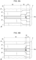
- FIG. 6A is a plan view of a first example in which the second section U2 has a different length.
- FIG. 6B is a plan view of a second example of the transmission line according to the embodiment in which the second section has a different length.
- FIG. 7A is a graph illustrating reflection characteristics in cases in which the second section is shorter.
- FIG. 7B is a graph illustrating the transmission characteristics of transmission lines in the cases in which the second section is shorter.
- FIG. 8A is a graph illustrating reflection characteristics in cases in which the second section is longer.
- FIG. 8B is a graph illustrating the transmission characteristics of transmission lines in the cases in which the second section is longer.
- FIGs. 7A, 7B , 8A, and 8B illustrate the frequency characteristics of the transmission lines in the cases in which the length of the second section U2 is (1/3) ⁇ H, (3/8) ⁇ H, (1/2) ⁇ H, (3/4) ⁇ H, 1 ⁇ H, (5/4) ⁇ H, and (3/2) ⁇ H.
- the length H is the distance between the signal conductor 22 and the second ground conductor 24.
- FIG. 9A is a plan view of variation 1 of the transmission line according to the embodiment.
- FIG. 9B is a graph illustrating the reflection characteristics of variation 1 of the transmission line according to the embodiment.
- FIG. 9C is a graph illustrating the transmission characteristics of variation 1 of the transmission line according to the embodiment.
- a signal line 20A of variation 1 includes step portions 221a and 221b at which the width of the signal conductor 22 decreases stepwise in an end portion of the third section U3 (on the side closer to the second section U2).
- the signal line 20A of variation 1 includes step portions 231a and 231b at which the distance between the signal conductor 22 and each first ground conductor 23 decreases stepwise on the inner sides (on the sides closer to the signal conductor 22) of the first ground conductors 23.
- the second section U2 does not include the step portions 221a, 221b, 231a, and 231b and has a length of from (1/3) ⁇ H to (3/2) ⁇ H.
- the signal line 20A includes the step portions 221a, 221b, 231a, and 23 1b in the third section U3, the signal line 20A provides good frequency characteristics as with the embodiment described above because the second section U2 has a length of from (1/3) ⁇ H to (3/2) ⁇ H.
- FIG. 10A is a cross-sectional perspective view of variation 2 of the transmission line according to the embodiment.
- FIG. 10B is a graph illustrating the reflection characteristics of variation 2 of the transmission line according to the embodiment.
- FIG. 10C is a graph illustrating the transmission characteristics of variation 2 of the transmission line according to the embodiment.
- Variation 2 is an example in which the diameter of an inner conductor 11B and the diameter of a pin terminal 11Ba of the coaxial line 10 are different.
- the pin terminal 11Ba has the same diameter as the pin terminal 11a of the embodiment in FIG. 3
- the inner conductor 11B is narrower than the inner conductor 11 of the embodiment in FIG. 3 .
- the pin terminal 11Ba has a larger diameter than the inner conductor 11.
- This configuration is referred to as variation 2a.
- a configuration in which both the pin terminal 11Ba and the inner conductor 11B are narrower than the pin terminal 11a and the inner conductor 11 of the embodiment in FIG. 3 is referred to as variation 2b.
- the diameter or the relative permittivity of the dielectric 12 is adjusted so that impedance mismatching will not occur in the coaxial line 10 due to the change in the diameter of the inner conductor 11B.
- variation 2b including the pin terminal 11Ba and the inner conductor 11B each having a smaller diameter, also provides good frequency characteristics in a high frequency range such as 80 GHz.
- Variation 2a which includes the pin terminal 11Ba having a larger diameter than the inner conductor 11B, provides better frequency characteristics than the embodiment in FIG. 3 and variation 2b in a high frequency range such as 80 GHz.
- the signal line 20 includes, in order from the coaxial line 10 side, the first section U1, the second section U2, and the third section U3, and the width wa2 of the signal conductor 22 in the second section U2 is constant, is less than or equal to the width wa1 of the signal conductor 22 in the first section U1, and is greater than the width wa3 of the signal conductor 22 in the third section U3.
- the distance wb2 between the signal conductor 22 and each first ground conductor 23 in the second section U2 is constant, is less than the distance wb1 in the first section U1, and is greater than the distance wb3 in the center portion U3c of the third section U3.
- the second section U2 has a length of from (1/3) ⁇ H to (3/2) ⁇ H on the side opposite to the coaxial line 10 from the position at which the distal end portion of the pin terminal 11a of the coaxial line 10 is present as viewed in the direction perpendicular to the first surface S1 of the insulation plate 21.
- This configuration makes it possible to achieve good frequency characteristics with a small reflection coefficient and a large transmission coefficient in a high frequency range such as 80 GHz.
- the width of the signal conductor 22 in the second section U2 is less than the width (the diameter w0) of the pin terminal 11a. This configuration makes it possible to achieve better frequency characteristics in a high frequency range such as 80 GHz.
- both sides ha2 and hb2 of the signal conductor 22 in the second section U2 are parallel to the longitudinal direction of the signal conductor 22.
- the sides hc2 and hd2 of the first ground conductors 23 closer to the signal conductor 22 are parallel to the longitudinal direction of the signal conductor 22.
- This configuration makes it possible to achieve better frequency characteristics in a high frequency range such as 80 GHz.
- the signal conductor 22 may include a curved shape.
- both sides of the signal conductor 22 in the second section U2 and the sides of the first ground conductors 23 closer to the signal conductor 22 may have a curved shape as with the signal conductor 22.
- the diameter of the pin terminal 11Ba of the coaxial line 10 is larger than the diameter of the inner conductor 11B. This configuration makes it possible to achieve better frequency characteristics in a high frequency range such as 80 GHz.
- the electronic device 100 of the present embodiment to which the package 1 for accommodating an electronic element is applied, achieves good frequency characteristics in a high frequency range such as 80 GHz.
- the present disclosure can be applied to packages for accommodating an electronic element and to electronic devices.
Landscapes
- Physics & Mathematics (AREA)
- Condensed Matter Physics & Semiconductors (AREA)
- General Physics & Mathematics (AREA)
- Electromagnetism (AREA)
- Optics & Photonics (AREA)
- Structure Of Printed Boards (AREA)
- Coupling Device And Connection With Printed Circuit (AREA)
Abstract
Description
- The present disclosure relates to a package for accommodating an electronic element and to an electronic device.
-
Japanese Unexamined Patent Application Publication No. 2007-123950 - A package for accommodating an electronic element according to the present disclosure includes:
- a base including a wall and an accommodating portion surrounded by the wall;
- a coaxial line located in the wall; and
- a signal line connected to the coaxial line on a side of the wall,
- the coaxial line includes a pin terminal protruding from the wall,
- the signal line includes an insulation plate including a first surface and a second surface on a side opposite to the first surface, a signal conductor located on the first surface and connected to the pin terminal, first ground conductors located on the first surface with the signal conductor interposed between the first ground conductors, and a second ground conductor located on the second surface,
- the signal line includes, in order from the coaxial line side, a first section, a second section, and a third section,
- a width of the signal conductor in the second section is constant, is less than or equal to a width of the signal conductor in the first section, and is greater than a width of the signal conductor in a center portion of the third section,
- a distance between the signal conductor and each of the first ground conductors is constant in the second section, is less than the distance in the first section, and is greater than the distance in the center portion of the third section, and
- the second section has a length of from 1/3 times to 3/2 times a distance H between the signal conductor and the second ground conductor on a side opposite to the coaxial line from a position at which a distal end portion of the pin terminal is present as viewed in a direction perpendicular to the first surface.
- An electronic device according to the present disclosure includes:
- the package for accommodating an electronic element, described above; and
- an electronic element accommodated in the package for accommodating an electronic element.
-
-
FIG. 1A is a cross-sectional view of a package for accommodating an electronic element and an electronic device according to an embodiment of the present disclosure. -
FIG. 1B is a plan view of the package for accommodating an electronic element and the electronic device according to the embodiment of the present disclosure. -
FIG. 2 is a cross-sectional perspective view of a portion including a transmission line of the package for accommodating an electronic element according to the embodiment. -
FIG. 3 is a plan view of the transmission line according to the embodiment. -
FIG. 4A is a graph illustrating the reflection characteristics of transmission lines of the embodiment and Comparative Examples 1 to 3. -
FIG. 4B is a graph illustrating the transmission characteristics of the transmission lines of the embodiment and Comparative Examples 1 to 3. -
FIG. 5A is a plan view of the transmission line of Comparative Example 1. -
FIG. 5B is a plan view of the transmission line of Comparative Example 2. -
FIG. 5C is a plan view of the transmission line of Comparative Example 3. -
FIG. 6A is a plan view of a first example of the transmission line according to the embodiment in which a second section has a different length. -
FIG. 6B is a plan view of a second example of the transmission line according to the embodiment in which the second section has a different length. -
FIG. 7A is a graph illustrating the reflection characteristics of transmission lines in cases in which the second section is shorter. -
FIG. 7B is a graph illustrating the transmission characteristics of the transmission lines in the cases in which the second section is shorter. -
FIG. 8A is a graph illustrating the reflection characteristics of transmission lines in cases in which the second section is longer. -
FIG. 8B is a graph illustrating the transmission characteristics of the transmission lines in the cases in which the second section is longer. -
FIG. 9A is a plan view ofvariation 1 of the transmission line according to the embodiment. -
FIG. 9B is a graph illustrating the reflection characteristics ofvariation 1 of the transmission line according to the embodiment. -
FIG. 9C is a graph illustrating the transmission characteristics ofvariation 1 of the transmission line according to the embodiment. -
FIG. 10A is a cross-sectional perspective view ofvariation 2 of the transmission line according to the embodiment. -
FIG. 10B is a graph illustrating the reflection characteristics ofvariation 2 of the transmission line according to the embodiment. -
FIG. 10C is a graph illustrating the transmission characteristics ofvariation 2 of the transmission line according to the embodiment. - Hereinafter, embodiments of the present disclosure will be described in detail with reference to the drawings.
-
FIG. 1A is a cross-sectional view of a package for accommodating an electronic element and an electronic device according to an embodiment of the present disclosure.FIG. 1B is a plan view of the package for accommodating an electronic element and the electronic device according to the embodiment of the present disclosure.FIG. 1A is a cross-sectional view taken along line A-A inFIG. 1B. FIG. 1B illustrates a configuration without alid 5. - The
electronic device 100 according to the embodiment of the present disclosure includes apackage 1 for accommodating an electronic element and anelectronic element 6 accommodated in anaccommodating portion 3 of thepackage 1 for accommodating an electronic element. Theelectronic element 6 is configured to perform both or one of receiving and outputting high-frequency signals and is, for example, a semiconductor laser element configured to convert high-frequency electrical signals into optical signals. Theelectronic element 6 may be an LN (LiNbO3) element configured to modulate laser light passing through an optical waveguide with high-frequency electrical signals. Besides these examples, theelectronic element 6 may be any element configured to perform both or one of receiving and outputting high-frequency signals and is not particularly limited. - The
package 1 for accommodating an electronic element includes a base 4 including awall 2 and theaccommodating portion 3 surrounded by thewall 2, acoaxial line 10 located in thewall 2, asignal line 20 located on a side of thewall 2, and thelid 5 closing an opening of theaccommodating portion 3. The base 4 may be made of a metal. Although thesignal line 20 is located inside the wall 2 (on theaccommodating portion 3 side), thesignal line 20 may be located outside thewall 2. Hereinafter, the combination of thecoaxial line 10 and thesignal line 20 is referred to as "transmission line". -
FIG. 2 is a cross-sectional perspective view of part of the transmission line of the package for accommodating an electronic element according to the embodiment.FIG. 3 is a plan view of the transmission line according to the embodiment. - As illustrated in
FIG. 2 , thecoaxial line 10 includes aninner conductor 11, which is a core line, a dielectric 12 located around theinner conductor 11, a tubularouter conductor 13 covering the radial outer side of theinner conductor 11, and apin terminal 11a continuous with theinner conductor 11 and protruding from the dielectric 12. Thepin terminal 11a extends along the center axis of theinner conductor 11. The space between theinner conductor 11 and theouter conductor 13 is sealed with the dielectric 12. - The
coaxial line 10 is located in the wall 2 (specifically, in a throughhole 2h of the wall 2) and transmits high-frequency signals between the inside and the outside of theaccommodating portion 3. Thepin terminal 11a protrudes from thewall 2 to the outside of the wall 2 (on theaccommodating portion 3 side). - As illustrated in
FIGs. 2 and 3 , thesignal line 20 is plate-shaped and includes aninsulation plate 21 including a first surface S1 and a second surface S2, asignal conductor 22 located on the first surface S1 and connected to thepin terminal 11a,first ground conductors 23 located on the first surface S1 with thesignal conductor 22 interposed between thefirst ground conductors 23, and asecond ground conductor 24 located on the second surface S2. The first surface S1 is located on a side opposite to the second surface S2. Theinsulation plate 21 is a dielectric and may be a ceramic. Thesignal line 20 may also be referred to as a coplanar line with a backside conductor. - The
signal conductor 22, thefirst ground conductors 23, and thesecond ground conductor 24 are film-shaped. Thesecond ground conductor 24 is opposed to thesignal conductor 22 and thefirst ground conductors 23 and spreads out on the second surface S2. - The
signal line 20 further includes a plurality of viaconductors 25 connecting thefirst ground conductors 23 and thesecond ground conductor 24. Each viaconductor 25 extends from the first surface S1 to the second surface S2 of theinsulation plate 21. InFIG. 2 , upper end portions of the viaconductors 25 are illustrated with dashed lines, and each viaconductor 25 extends in the direction perpendicular to the first surface S1 from the first surface S1 to the second surface S2. - The width and thickness of the
signal conductor 22, the distance between thesignal conductor 22 and eachfirst ground conductor 23, the distance between thesignal conductor 22 and thesecond ground conductor 24, and the intervals between the plurality of viaconductors 25 are set according to the frequency of a transmission signal and the relative permittivity of theinsulation plate 21 so as to achieve specified impedance matching. The signal frequency is assumed to be in an 80 GHz band or higher. The distance H between thesignal conductor 22 and thesecond ground conductor 24 is 1/4 or less of the effective wavelength of a high-frequency signal, and the intervals of the plurality of viaconductors 25 are 1/2 or less of the effective wavelength of the high-frequency signal. - Since the periphery of the connection portion between the
signal line 20 and thecoaxial line 10 is a portion where the transmission mode of a high-frequency signal changes, the dimensions and shape of thesignal conductor 22 in this portion and the dimensions and shapes of the portions between thesignal conductor 22 and thefirst ground conductors 23 are different from those of the other portions of thesignal line 20. - As illustrated in
FIG. 3 , thesignal line 20 includes, in order from thecoaxial line 10 side in the direction of thesignal conductor 22, a first section U1, a second section U2, and a third section U3. - The first section U1 is from the end of the
signal line 20 on thewall 2 side to the position at which the distal end portion of thepin terminal 11a is present as viewed in the direction perpendicular to the first surface S1. The second section U2 has a length of from H/3 to 3H/2 in a direction opposite to thecoaxial line 10 from the position at which the distal end portion of thepin terminal 11a is present as viewed in the direction perpendicular to the first surface S1. The third section U3 is from the end of the second section U2 on a side opposite to thecoaxial line 10 to the end of thesignal line 20 on the side opposite to thecoaxial line 10. The length H mentioned above is the distance between thesignal conductor 22 and thesecond ground conductor 24. The distal end portion of thepin terminal 11a corresponds to not only the distal end of thepin terminal 11a in the strict sense but also a portion having a slight width from the distal end toward the proximal end. The slight width may be a length to a degree that the influence on high-frequency signal transmission characteristics can be disregarded and corresponds to, for example, a length of 1/16 or less of the effective wavelength λ of a high-frequency signal. - In a main range of the third section U3, the width wa3 of the
signal conductor 22 is constant, and the distance wb3 between thesignal conductor 22 and eachfirst ground conductor 23 is constant. However, since a portion close to the end of thesignal line 20 is connected to another transmission line, the shapes and dimensions of thesignal conductor 22 and thefirst ground conductors 23 may be different from those in a center portion U3c of the third section U3. In the third section U3, since portions adjoining the second section U2 are continuous with thesignal conductor 22 and thefirst ground conductors 23 in the second section U2, these portions may include a slope or a round shape. In other words, although the width wa3 of thesignal conductor 22 and the distance wb3 between thesignal conductor 22 and eachfirst ground conductor 23 are not constant in a start end portion and a terminal end portion of the third section U3, they are constant in the center portion U3c of the third section U3. - In the first section U1, the width wa1 of the
signal conductor 22 is greater than the width wa3 in the center portion U3c of the third section U3, and the distance wb1 between thesignal conductor 22 and eachfirst ground conductor 23 is greater than the distance wb3 in the third section U3. - In the first section U1, the left and right sides ha1 and hb1 of the
signal conductor 22 may include portions parallel to the longitudinal direction of thesignal conductor 22. The longitudinal direction of thesignal conductor 22 is the direction along the center line passing through the center of the width of thesignal conductor 22. In the first section U1, two inner sides hc1 and hd1 (on the sides closer to the signal conductor 22) of thefirst ground conductors 23 may include portions parallel to the longitudinal direction of thesignal conductor 22. - In the second section U2, the width wa2 of the
signal conductor 22 is constant, is less than or equal to the width wa1 in the first section U1, and is greater than the width wa3 in the third section U3. In the second section U2, the distance wb2 between thesignal conductor 22 and eachfirst ground conductor 23 is constant, is less than the distance wb1 mentioned above in the first section U1, and is greater than the distance wb3 mentioned above in the center portion U3c of the third section U3. - In the second section U2, the left and right sides ha2 and hb2 of the
signal conductor 22 are parallel to the longitudinal direction of thesignal conductor 22. The longitudinal direction of thesignal conductor 22 is the direction along the center line passing through the center of the width of thesignal conductor 22. In the second section U2, two inner sides hc2 and hd2 (on the sides closer to the signal conductor 22) of thefirst ground conductors 23 are parallel to the longitudinal direction of thesignal conductor 22. - In the second section U2, the width wa2 of the
signal conductor 22 is less than the diameter w0 of thepin terminal 11a. The width wa1 of thesignal conductor 22 in the first section U1 may be less than the diameter w0 of thepin terminal 11a and may be equal to the width wa2 in the second section U2. - The
pin terminal 11a is joined mainly to thesignal conductor 22 in the first section U1 with a conductive joining material e interposed therebetween. -
FIG. 4A is a graph illustrating the reflection characteristics of transmission lines of the embodiment and Comparative Examples 1 to 3.FIG. 4B is a graph illustrating the transmission characteristics of the transmission lines of the embodiment and Comparative Examples 1 to 3.FIGs. 5A to 5C are plan views oftransmission lines 81 to 83 of Comparative Examples 1 to 3, respectively. - As indicated by the characteristics lines of the embodiment in
FIG. 4 , the simulation results indicate that the transmission line of thepackage 1 for accommodating an electronic element according to the present embodiment provides good frequency characteristics in which the return loss and the insertion loss are low, in other words, the reflection coefficient is small and the transmission coefficient is large, in a high frequency range such as 80 GHz. - In the plate-shaped signal line 20 (a coplanar line with a backside conductor), the width of the
signal conductor 22 and the distance between thesignal conductor 22 and eachfirst ground conductor 23 are limited by the requirement with respect to frequency characteristics, except for sections close to the start end or the terminal end. In the first section U1 where thesignal line 20 is connected to thepin terminal 11a, the shape and dimensions of thesignal conductor 22 and the shapes and dimensions of the portions between thesignal conductor 22 and thefirst ground conductors 23 are limited to meet requirements with respect to the frequency characteristics, the strength, and the like. Specifically, the width of thesignal conductor 22 in the first section U1 is designed to be greater than the width in the center portion U3c of the third section U3, and the distance between thesignal conductor 22 and eachfirst ground conductor 23 in the first section U1 is designed to be greater than the distance in the center portion U3c of the third section U3. - In the
transmission lines 81 to 83 of the comparative examples inFIGs. 5A to 5C , thesignal conductor 22 and the portions between thesignal conductor 22 and thefirst ground conductors 23 in the first section U1 and the third section U3 have shapes and dimensions that are the same as and/or similar to those in the embodiment inFIG. 3 . In the second section U2, the shapes and dimensions of thesignal conductor 22 and the portions between thesignal conductor 22 and thefirst ground conductors 23 are different from those of the embodiment inFIG. 3 . - The
transmission line 81 inFIG. 5A is an example in which thesignal conductor 22 and thefirst ground conductors 23 have a tapered shape in the second section U2 so that thesignal conductor 22 and thefirst ground conductors 23 in the first section U1 are connected to thesignal conductor 22 and thefirst ground conductors 23 in the third section U3 without a step. - The
transmission line 82 inFIG. 5B is an example in which the width of thesignal conductor 22 is large approximately only at a portion connected to thepin terminal 11a, and the distance between thesignal conductor 22 and eachfirst ground conductor 23 decreases stepwise. In Comparative Example 2, the shapes and dimensions of the sides of thefirst ground conductors 23 facing thesignal conductor 22 are the same as and/or similar to those in the embodiment inFIG. 3 . - The transmission line 83 in
FIG. 5C is an example in which the width of thesignal conductor 22 is large from the first section U1 to the second section U2 as with the portion connected to thepin terminal 11a, and the distance between thesignal conductor 22 and eachfirst ground conductor 23 is also large in the second section U2 as in the first section U1. In Comparative Example 3, the shape and dimensions of thesignal conductor 22 are the same as and/or similar to those in the embodiment inFIG. 3 . - The transmission line of the
package 1 for accommodating an electronic element according to the embodiment is different from thetransmission lines 81 to 83 of Comparative Examples 1 to 3 in the shape and dimensions of thesignal conductor 22 and the shapes and dimensions of the portions between thesignal conductor 22 and thefirst ground conductors 23 in the second section U2. - As indicated by the simulation results in
FIGs. 4A and 4B , the transmission line of thepackage 1 for accommodating an electronic element according to the embodiment has significantly good frequency characteristics in a high frequency range such as 80 GHz, even when compared with thetransmission lines 81 to 83 of Comparative Examples 1 to 3. -
FIG. 6A is a plan view of a first example in which the second section U2 has a different length.FIG. 6B is a plan view of a second example of the transmission line according to the embodiment in which the second section has a different length.FIG. 7A is a graph illustrating reflection characteristics in cases in which the second section is shorter.FIG. 7B is a graph illustrating the transmission characteristics of transmission lines in the cases in which the second section is shorter.FIG. 8A is a graph illustrating reflection characteristics in cases in which the second section is longer.FIG. 8B is a graph illustrating the transmission characteristics of transmission lines in the cases in which the second section is longer. - As illustrated in
FIGs. 6A and 6B , different lengths of the second section U2 make a difference in the frequency characteristics of the transmission line.FIGs. 7A, 7B ,8A, and 8B illustrate the frequency characteristics of the transmission lines in the cases in which the length of the second section U2 is (1/3) × H, (3/8) × H, (1/2) × H, (3/4) × H, 1 × H, (5/4) × H, and (3/2) × H. The length H is the distance between thesignal conductor 22 and thesecond ground conductor 24. - As illustrated in
FIGs. 7A, 7B ,8A, and 8B , in the case in which the length of the second section U2 is from (1/3) × H to (3/2) × H, the frequency characteristics are good, and in the case in which the length of the second section U2 is from (1/2) × H to 1 × H, the frequency characteristics are better. -
FIG. 9A is a plan view ofvariation 1 of the transmission line according to the embodiment.FIG. 9B is a graph illustrating the reflection characteristics ofvariation 1 of the transmission line according to the embodiment.FIG. 9C is a graph illustrating the transmission characteristics ofvariation 1 of the transmission line according to the embodiment. As illustrated inFIG. 9A , asignal line 20A ofvariation 1 includes step portions 221a and 221b at which the width of thesignal conductor 22 decreases stepwise in an end portion of the third section U3 (on the side closer to the second section U2). In addition, thesignal line 20A ofvariation 1 includes step portions 231a and 231b at which the distance between thesignal conductor 22 and eachfirst ground conductor 23 decreases stepwise on the inner sides (on the sides closer to the signal conductor 22) of thefirst ground conductors 23. - In the
signal line 20A ofvariation 1, the second section U2 does not include the step portions 221a, 221b, 231a, and 231b and has a length of from (1/3) × H to (3/2) × H. - As illustrated in
FIGs. 9B and 9C , although thesignal line 20A includes thestep portions 221a, 221b, 231a, and 23 1b in the third section U3, thesignal line 20A provides good frequency characteristics as with the embodiment described above because the second section U2 has a length of from (1/3) × H to (3/2) × H. -
FIG. 10A is a cross-sectional perspective view ofvariation 2 of the transmission line according to the embodiment.FIG. 10B is a graph illustrating the reflection characteristics ofvariation 2 of the transmission line according to the embodiment.FIG. 10C is a graph illustrating the transmission characteristics ofvariation 2 of the transmission line according to the embodiment.Variation 2 is an example in which the diameter of aninner conductor 11B and the diameter of a pin terminal 11Ba of thecoaxial line 10 are different. In the example ofFIG. 10A , the pin terminal 11Ba has the same diameter as thepin terminal 11a of the embodiment inFIG. 3 , and theinner conductor 11B is narrower than theinner conductor 11 of the embodiment inFIG. 3 . In other words, the pin terminal 11Ba has a larger diameter than theinner conductor 11. This configuration is referred to asvariation 2a. In addition, a configuration in which both the pin terminal 11Ba and theinner conductor 11B are narrower than thepin terminal 11a and theinner conductor 11 of the embodiment inFIG. 3 is referred to asvariation 2b. Note that invariations coaxial line 10 due to the change in the diameter of theinner conductor 11B. - As illustrated in
FIGs. 10B and 10C ,variation 2b, including the pin terminal 11Ba and theinner conductor 11B each having a smaller diameter, also provides good frequency characteristics in a high frequency range such as 80 GHz.Variation 2a, which includes the pin terminal 11Ba having a larger diameter than theinner conductor 11B, provides better frequency characteristics than the embodiment inFIG. 3 andvariation 2b in a high frequency range such as 80 GHz. - As described above, in the
package 1 for accommodating an electronic element according to the present embodiment, thesignal line 20 includes, in order from thecoaxial line 10 side, the first section U1, the second section U2, and the third section U3, and the width wa2 of thesignal conductor 22 in the second section U2 is constant, is less than or equal to the width wa1 of thesignal conductor 22 in the first section U1, and is greater than the width wa3 of thesignal conductor 22 in the third section U3. The distance wb2 between thesignal conductor 22 and eachfirst ground conductor 23 in the second section U2 is constant, is less than the distance wb1 in the first section U1, and is greater than the distance wb3 in the center portion U3c of the third section U3. The second section U2 has a length of from (1/3) × H to (3/2) × H on the side opposite to thecoaxial line 10 from the position at which the distal end portion of thepin terminal 11a of thecoaxial line 10 is present as viewed in the direction perpendicular to the first surface S1 of theinsulation plate 21. This configuration makes it possible to achieve good frequency characteristics with a small reflection coefficient and a large transmission coefficient in a high frequency range such as 80 GHz. - In the
package 1 for accommodating an electronic element according to the present embodiment, the width of thesignal conductor 22 in the second section U2 is less than the width (the diameter w0) of thepin terminal 11a. This configuration makes it possible to achieve better frequency characteristics in a high frequency range such as 80 GHz. - In the
package 1 for accommodating an electronic element according to the present embodiment, both sides ha2 and hb2 of thesignal conductor 22 in the second section U2 are parallel to the longitudinal direction of thesignal conductor 22. In addition, the sides hc2 and hd2 of thefirst ground conductors 23 closer to thesignal conductor 22 are parallel to the longitudinal direction of thesignal conductor 22. This configuration makes it possible to achieve better frequency characteristics in a high frequency range such as 80 GHz. Note that thesignal conductor 22 may include a curved shape. In this case, both sides of thesignal conductor 22 in the second section U2 and the sides of thefirst ground conductors 23 closer to thesignal conductor 22 may have a curved shape as with thesignal conductor 22. - In the
package 1 for accommodating an electronic element according tovariation 2a, the diameter of the pin terminal 11Ba of thecoaxial line 10 is larger than the diameter of theinner conductor 11B. This configuration makes it possible to achieve better frequency characteristics in a high frequency range such as 80 GHz. - The
electronic device 100 of the present embodiment, to which thepackage 1 for accommodating an electronic element is applied, achieves good frequency characteristics in a high frequency range such as 80 GHz. - The embodiment of the present disclosure has been described above. However, the package for accommodating an electronic element and the electronic device according to the present disclosure are not limited to the above embodiment and can be modified as appropriate without departing from the spirit of the invention.
- The present disclosure can be applied to packages for accommodating an electronic element and to electronic devices.
-
- 1 package for accommodating electronic element
- 2 wall
- 3 accommodating portion
- 4 base
- 5 lid
- 6 electronic element
- 10 coaxial line
- 11, 11B inner conductor
- 12 dielectric
- 13 outer conductor
- 11a, 11Ba pin terminal
- w0 diameter of pin terminal
- 20 signal line
- 21 insulation plate
- S1 first surface
- S2 second surface
- 22 signal conductor
- 23 first ground conductor
- 24 second ground conductor
- 25 via conductor
- e joining material
- U1 first section
- U2 second section
- U3 third section
- wa1, wa2, wa3 width of signal conductor
- wb1, wb2, wb3 distance between signal conductor and each first ground conductor
- ha1, hb1, hc1, hd1, ha2, hb2, hc2, hd2 side
- 100 electronic device
Claims (5)
- A package for accommodating an electronic element, comprising:a base comprising a wall and an accommodating portion surrounded by the wall;a coaxial line located in the wall; anda signal line connected to the coaxial line on a side of the wall, whereinthe coaxial line comprises a pin terminal protruding from the wall,the signal line comprises an insulation plate comprising a first surface and a second surface on a side opposite to the first surface, a signal conductor located on the first surface and connected to the pin terminal, first ground conductors located on the first surface with the signal conductor interposed between the first ground conductors, and a second ground conductor located on the second surface,the signal line includes, in order from the coaxial line side, a first section, a second section, and a third section,a width of the signal conductor in the second section is constant, is less than or equal to a width of the signal conductor in the first section, and is greater than a width of the signal conductor in a center portion of the third section,a distance between the signal conductor and each of the first ground conductors is constant in the second section, is less than the distance in the first section, and is greater than the distance in the center portion of the third section, andthe second section has a length of from 1/3 times to 3/2 times a distance H between the signal conductor and the second ground conductor on a side opposite to the coaxial line from a position at which a distal end portion of the pin terminal is present as viewed in a direction perpendicular to the first surface.
- The package for accommodating an electronic element according to claim 1, wherein
the width of the signal conductor in the second section is less than a width of the pin terminal. - The package for accommodating an electronic element according to claim 1 or 2, whereinboth sides of the signal conductor in the second section are parallel to a longitudinal direction of the signal conductor, andsides of the first ground conductors closer to the signal conductor in the second section are parallel to the longitudinal direction of the signal conductor.
- The package for accommodating an electronic element according to any one of claims 1 to 3, whereinthe coaxial line further comprises an inner conductor continuous with the pin terminal and a dielectric located around the inner conductor, anda diameter of the pin terminal is larger than a diameter of the inner conductor.
- An electronic device comprising:the package for accommodating an electronic element according to any one of claims 1 to 4; andan electronic element accommodated in the accommodating portion.
Applications Claiming Priority (2)
| Application Number | Priority Date | Filing Date | Title |
|---|---|---|---|
| JP2021068471 | 2021-04-14 | ||
| PCT/JP2022/017091 WO2022220176A1 (en) | 2021-04-14 | 2022-04-05 | Package for accommodating electronic element, and electronic device |
Publications (2)
| Publication Number | Publication Date |
|---|---|
| EP4325656A1 true EP4325656A1 (en) | 2024-02-21 |
| EP4325656A4 EP4325656A4 (en) | 2025-04-02 |
Family
ID=83639646
Family Applications (1)
| Application Number | Title | Priority Date | Filing Date |
|---|---|---|---|
| EP22788101.8A Pending EP4325656A4 (en) | 2021-04-14 | 2022-04-05 | Package for accommodating electronic element, and electronic device |
Country Status (5)
| Country | Link |
|---|---|
| US (1) | US20240195142A1 (en) |
| EP (1) | EP4325656A4 (en) |
| JP (1) | JP7559224B2 (en) |
| CN (1) | CN117121292A (en) |
| WO (1) | WO2022220176A1 (en) |
Families Citing this family (2)
| Publication number | Priority date | Publication date | Assignee | Title |
|---|---|---|---|---|
| US12456790B2 (en) * | 2021-07-09 | 2025-10-28 | Kyocera Corporation | Electronic element storing package and electronic device |
| JP7711114B2 (en) * | 2023-03-02 | 2025-07-22 | アンリツ株式会社 | Package and transmission line connection structure |
Family Cites Families (7)
| Publication number | Priority date | Publication date | Assignee | Title |
|---|---|---|---|---|
| WO2002047172A1 (en) | 2000-12-08 | 2002-06-13 | Sophia Wireless, Inc. | A high frequency interconnect system using micromachined plugs and sockets |
| US7088489B2 (en) * | 2002-10-04 | 2006-08-08 | Jds Uniphase Corporation | Launch interface electrode structure for suppressing coupling to substrate modes for electro-optic modulator |
| DE10345218B3 (en) * | 2003-09-29 | 2004-12-30 | Siemens Ag | Coplanar end connection for coaxial cable has central tapering conductor for solid circular-cross-section inner conductor and two tapering outer conductors connected to square terminal on cable sheath |
| JP2007123950A (en) | 2004-01-09 | 2007-05-17 | Nec Corp | Coaxial line-flat substrate conversion structure and high-frequency signal converter |
| JP4056545B2 (en) | 2006-04-04 | 2008-03-05 | 住友大阪セメント株式会社 | High frequency line connection structure |
| JP5241609B2 (en) | 2008-06-19 | 2013-07-17 | 京セラ株式会社 | Structure, connection terminal, package, and electronic device |
| JP2017069138A (en) | 2015-10-01 | 2017-04-06 | 三菱電機株式会社 | Connector, transceiver module, and method of manufacturing transceiver module |
-
2022
- 2022-04-05 JP JP2023514618A patent/JP7559224B2/en active Active
- 2022-04-05 US US18/286,856 patent/US20240195142A1/en active Pending
- 2022-04-05 WO PCT/JP2022/017091 patent/WO2022220176A1/en not_active Ceased
- 2022-04-05 CN CN202280027879.1A patent/CN117121292A/en active Pending
- 2022-04-05 EP EP22788101.8A patent/EP4325656A4/en active Pending
Also Published As
| Publication number | Publication date |
|---|---|
| EP4325656A4 (en) | 2025-04-02 |
| US20240195142A1 (en) | 2024-06-13 |
| WO2022220176A1 (en) | 2022-10-20 |
| CN117121292A (en) | 2023-11-24 |
| JPWO2022220176A1 (en) | 2022-10-20 |
| JP7559224B2 (en) | 2024-10-01 |
Similar Documents
| Publication | Publication Date | Title |
|---|---|---|
| EP3414789B1 (en) | A transition arrangement comprising a contactless transition or connection between an siw and a waveguide or an antenna | |
| US8089327B2 (en) | Waveguide to plural microstrip transition | |
| KR100443139B1 (en) | Coaxial connector and connection structure including the same | |
| US5414394A (en) | Microwave frequency device comprising at least a transition between a transmission line integrated on a substrate and a waveguide | |
| CN1694304B (en) | Contactless transition element between wave guide and micro strip line | |
| US7199680B2 (en) | RF module using mode converting structure having short-circuiting waveguides and connecting windows | |
| EP4325656A1 (en) | Package for accommodating electronic element, and electronic device | |
| CN100588118C (en) | Adaptive Transmission Line Connectors | |
| US20050200424A1 (en) | Microstripline waveguide converter | |
| US5969580A (en) | Transition between a ridge waveguide and a planar circuit which faces in the same direction | |
| US11101535B2 (en) | Transmission line-waveguide transition device comprising a waveguide having a ridge connected to the transmission line at a reduced width ground transition area | |
| US5801528A (en) | Semiconductor element evaluating apparatus | |
| KR100263640B1 (en) | Planer dielectric integrated circuit | |
| US10950920B2 (en) | Transition between a tubular waveguide body and an external planar connection portion through a planar matching ridge in the waveguide body | |
| KR20040036021A (en) | PCB Coaxial Connector | |
| EP3872927B1 (en) | Dielectric waveguide connector | |
| JP2001094012A (en) | Semiconductor chip mounting substrate and high frequency device | |
| US7541886B2 (en) | NRD guide transition, and coupling structure of dielectric material and conductor | |
| US20250015473A1 (en) | Transition circuit and communication device | |
| EP4415157A1 (en) | External port | |
| JP7113986B2 (en) | Converter and antenna device | |
| KR101759286B1 (en) | Transition waveguide and transition element | |
| JP4821391B2 (en) | Circuit board connection structure | |
| JP2001217332A (en) | High frequency circuit package | |
| JP2024171387A (en) | Planar line to waveguide transition |
Legal Events
| Date | Code | Title | Description |
|---|---|---|---|
| STAA | Information on the status of an ep patent application or granted ep patent |
Free format text: STATUS: THE INTERNATIONAL PUBLICATION HAS BEEN MADE |
|
| PUAI | Public reference made under article 153(3) epc to a published international application that has entered the european phase |
Free format text: ORIGINAL CODE: 0009012 |
|
| STAA | Information on the status of an ep patent application or granted ep patent |
Free format text: STATUS: REQUEST FOR EXAMINATION WAS MADE |
|
| 17P | Request for examination filed |
Effective date: 20231012 |
|
| AK | Designated contracting states |
Kind code of ref document: A1 Designated state(s): AL AT BE BG CH CY CZ DE DK EE ES FI FR GB GR HR HU IE IS IT LI LT LU LV MC MK MT NL NO PL PT RO RS SE SI SK SM TR |
|
| DAV | Request for validation of the european patent (deleted) | ||
| DAX | Request for extension of the european patent (deleted) | ||
| A4 | Supplementary search report drawn up and despatched |
Effective date: 20250227 |
|
| RIC1 | Information provided on ipc code assigned before grant |
Ipc: H01P 5/08 20060101AFI20250221BHEP |