EP4325498A1 - Refresh control circuit and method therefor, and memory - Google Patents
Refresh control circuit and method therefor, and memory Download PDFInfo
- Publication number
- EP4325498A1 EP4325498A1 EP22834833.0A EP22834833A EP4325498A1 EP 4325498 A1 EP4325498 A1 EP 4325498A1 EP 22834833 A EP22834833 A EP 22834833A EP 4325498 A1 EP4325498 A1 EP 4325498A1
- Authority
- EP
- European Patent Office
- Prior art keywords
- signal
- block
- refresh
- output
- address
- Prior art date
- Legal status (The legal status is an assumption and is not a legal conclusion. Google has not performed a legal analysis and makes no representation as to the accuracy of the status listed.)
- Withdrawn
Links
Images




Classifications
-
- G—PHYSICS
- G11—INFORMATION STORAGE
- G11C—STATIC STORES
- G11C11/00—Digital stores characterised by the use of particular electric or magnetic storage elements; Storage elements therefor
- G11C11/21—Digital stores characterised by the use of particular electric or magnetic storage elements; Storage elements therefor using electric elements
- G11C11/34—Digital stores characterised by the use of particular electric or magnetic storage elements; Storage elements therefor using electric elements using semiconductor devices
- G11C11/40—Digital stores characterised by the use of particular electric or magnetic storage elements; Storage elements therefor using electric elements using semiconductor devices using transistors
- G11C11/401—Digital stores characterised by the use of particular electric or magnetic storage elements; Storage elements therefor using electric elements using semiconductor devices using transistors forming cells needing refreshing or charge regeneration, i.e. dynamic cells
- G11C11/406—Management or control of the refreshing or charge-regeneration cycles
- G11C11/40611—External triggering or timing of internal or partially internal refresh operations, e.g. auto-refresh or CAS-before-RAS triggered refresh
-
- G—PHYSICS
- G11—INFORMATION STORAGE
- G11C—STATIC STORES
- G11C11/00—Digital stores characterised by the use of particular electric or magnetic storage elements; Storage elements therefor
- G11C11/21—Digital stores characterised by the use of particular electric or magnetic storage elements; Storage elements therefor using electric elements
- G11C11/34—Digital stores characterised by the use of particular electric or magnetic storage elements; Storage elements therefor using electric elements using semiconductor devices
- G11C11/40—Digital stores characterised by the use of particular electric or magnetic storage elements; Storage elements therefor using electric elements using semiconductor devices using transistors
- G11C11/401—Digital stores characterised by the use of particular electric or magnetic storage elements; Storage elements therefor using electric elements using semiconductor devices using transistors forming cells needing refreshing or charge regeneration, i.e. dynamic cells
- G11C11/406—Management or control of the refreshing or charge-regeneration cycles
- G11C11/40622—Partial refresh of memory arrays
-
- G—PHYSICS
- G11—INFORMATION STORAGE
- G11C—STATIC STORES
- G11C11/00—Digital stores characterised by the use of particular electric or magnetic storage elements; Storage elements therefor
- G11C11/21—Digital stores characterised by the use of particular electric or magnetic storage elements; Storage elements therefor using electric elements
- G11C11/34—Digital stores characterised by the use of particular electric or magnetic storage elements; Storage elements therefor using electric elements using semiconductor devices
- G11C11/40—Digital stores characterised by the use of particular electric or magnetic storage elements; Storage elements therefor using electric elements using semiconductor devices using transistors
- G11C11/401—Digital stores characterised by the use of particular electric or magnetic storage elements; Storage elements therefor using electric elements using semiconductor devices using transistors forming cells needing refreshing or charge regeneration, i.e. dynamic cells
- G11C11/4063—Auxiliary circuits, e.g. for addressing, decoding, driving, writing, sensing or timing
- G11C11/407—Auxiliary circuits, e.g. for addressing, decoding, driving, writing, sensing or timing for memory cells of the field-effect type
- G11C11/408—Address circuits
- G11C11/4085—Word line control circuits, e.g. word line drivers, - boosters, - pull-up, - pull-down, - precharge
-
- G—PHYSICS
- G11—INFORMATION STORAGE
- G11C—STATIC STORES
- G11C11/00—Digital stores characterised by the use of particular electric or magnetic storage elements; Storage elements therefor
- G11C11/21—Digital stores characterised by the use of particular electric or magnetic storage elements; Storage elements therefor using electric elements
- G11C11/34—Digital stores characterised by the use of particular electric or magnetic storage elements; Storage elements therefor using electric elements using semiconductor devices
- G11C11/40—Digital stores characterised by the use of particular electric or magnetic storage elements; Storage elements therefor using electric elements using semiconductor devices using transistors
- G11C11/401—Digital stores characterised by the use of particular electric or magnetic storage elements; Storage elements therefor using electric elements using semiconductor devices using transistors forming cells needing refreshing or charge regeneration, i.e. dynamic cells
- G11C11/4063—Auxiliary circuits, e.g. for addressing, decoding, driving, writing, sensing or timing
- G11C11/407—Auxiliary circuits, e.g. for addressing, decoding, driving, writing, sensing or timing for memory cells of the field-effect type
- G11C11/408—Address circuits
- G11C11/4087—Address decoders, e.g. bit - or word line decoders; Multiple line decoders
-
- Y—GENERAL TAGGING OF NEW TECHNOLOGICAL DEVELOPMENTS; GENERAL TAGGING OF CROSS-SECTIONAL TECHNOLOGIES SPANNING OVER SEVERAL SECTIONS OF THE IPC; TECHNICAL SUBJECTS COVERED BY FORMER USPC CROSS-REFERENCE ART COLLECTIONS [XRACs] AND DIGESTS
- Y02—TECHNOLOGIES OR APPLICATIONS FOR MITIGATION OR ADAPTATION AGAINST CLIMATE CHANGE
- Y02D—CLIMATE CHANGE MITIGATION TECHNOLOGIES IN INFORMATION AND COMMUNICATION TECHNOLOGIES [ICT], I.E. INFORMATION AND COMMUNICATION TECHNOLOGIES AIMING AT THE REDUCTION OF THEIR OWN ENERGY USE
- Y02D10/00—Energy efficient computing, e.g. low power processors, power management or thermal management
Definitions
- the present invention relates to the technical field of semiconductor memories, in particular to a refresh control circuit and method, and a memory.
- Row Hammer attacks are a kind of data attacks directed at a Dynamic Random Access Memory (DRAM), which cause data loss of adjacent Word Lines (WLs) (hereinafter referred to as victim WL) by frequently refreshing a certain WL (hereinafter referred to as hammer WL) in a short time.
- victim WL data loss of adjacent Word Lines
- hammer WL a certain WL
- the victim WLs need to be refreshed to recover the affected data, also known as a hammer refresh operation.
- the hammer refresh operation needs to be implemented by means of a general refresh operation process, which causes some irrelevant WLs to be additionally refreshed during the hammer refresh process, resulting in a waste of resources and reducing the performance of the memory.
- the present invention provides a refresh control circuit and method, and a memory, which can reduce the number of irrelevant word lines (WLs) being refreshed in a hammer refresh operation and reduce refresh current and power consumption.
- WLs irrelevant word lines
- embodiments of the present invention provide a refresh control circuit.
- the refresh control circuit is connected with a memory array and includes: an address output module, a block decoding module, and a row decoding module.
- the address output module may be configured to output a to-be-refreshed address signal.
- the to-be-refreshed address signal includes a block address signal and a row address signal.
- the block decoding module is configured to receive the block address signal, decode the block address signal and output a first block selection signal, in response to that the memory array is subjected to no row hammer attack, or decode the block address signal and output a second block selection signal, in response to that the memory array is subjected to a row hammer attack.
- the first block selection signal is used for selecting multiple data blocks from the memory array
- the second block selection signal is used for selecting one data block from the memory array.
- the row decoding module may be configured to receive the row address signal, decode the row address signal, and output a row selection signal.
- the row selection signal is used for selecting a target refresh word line (WL) from the one data block selected by the second block selection signal, or selecting target refresh WLs from the multiple data blocks selected by the first block selection signal.
- the block decoding module may include: a preprocessing module, configured to receive a first row hammer signal, a refresh instruction signal and the block address signal; in response to that the first row hammer signal is invalid, perform first preprocessing on the block address signal based on the refresh instruction signal to obtain a block preselection signal, or in response to that the first row hammer signal is valid, perform second preprocessing based on the block address signal to obtain the block preselection signal; and a decoding module, configured to receive the block preselection signal, and decode the block preselection signal to obtain the first block selection signal or the second block selection signal.
- a preprocessing module configured to receive a first row hammer signal, a refresh instruction signal and the block address signal; in response to that the first row hammer signal is invalid, perform first preprocessing on the block address signal based on the refresh instruction signal to obtain a block preselection signal, or in response to that the first row hammer signal is valid, perform second preprocessing based on the block address signal to obtain the block prese
- the block address signal may include a first-type signal and a second-type signal.
- the block preselection signal may include a first signal pair and a second signal pair.
- the preprocessing module may include: a first processing module and a second processing module.
- the first processing module may be configured to receive the first-type signal, perform logical processing on the first-type signal, and output the first signal pair.
- the first signal pair may include the first-type signal and an inverted signal of the first-type signal, and a level state of the first-type signal is opposite to a level state of the inverted signal of the first-type signal.
- the second processing module may be configured to receive the first row hammer signal, the refresh instruction signal and the second-type signal; and perform the first preprocessing or the second preprocessing on the second-type signal based on the first row hammer signal and the refresh instruction signal, and output the second signal pair.
- the second signal pair may include the second-type signal and an inverted signal of the second-type signal.
- a level state of the second-type signal is opposite to a level state of the inverted signal of the second-type signal are opposite; and in response to that the first row hammer signal is invalid and the refresh instruction signal is valid, the second-type signal and the inverted signal of the second-type signal are both set to be in a high-level state.
- the first processing module may include a first NOT gate.
- An input end of the first NOT gate receives the first-type signal, and an output end of the first NOT gate outputs the inverted signal of the first-type signal.
- the second processing module may include: an enable module and a logic module.
- the enable module may be configured to receive the first row hammer signal and the refresh instruction signal, and output an operation control signal.
- the operation control signal is valid in response to that the first row hammer signal is invalid and the refresh instruction signal is valid.
- the operation control signal is valid.
- the operation control signal is invalid.
- the logic module may be configured to receive the operation control signal and the second-type signal; perform the first preprocessing on the second-type signal and output the second signal pair, in response to that the operation control signal is valid; and perform the second preprocessing on the second-type signal and output the second signal pair, in response to that the operation control signal is invalid.
- the enable module may include a second NOT gate, a first NAND gate and a third NOT gate.
- an input end of the second NOT gate receives the first row hammer signal
- a first input end of the first NAND gate is connected with an output end of the second NOT gate
- a second input end of the first NAND gate receives the refresh instruction signal
- an output end of the first NAND gate is connected with the input end of the third NOT gate
- an output end of the third NOT gate is configured to output the operation control signal.
- the logic module may include a fourth NOT gate, a second NAND gate, a fifth NOT gate, and a third NAND gate.
- the fourth NOT gate receives the operation control signal
- a first input end of the second NAND gate is connected with an output end of the fourth NOT gate
- a second input end of the second NAND gate receives the second-type signal
- an output end of the second NAND gate is configured to output the inverted signal of the second-type signal.
- An input end of the fifth NOT gate receives the second-type signal
- a first input end of the third NAND gate is connected with an output end of the fourth NOT gate
- a second input end of the third NAND gate is connected with an output end of the fifth NOT gate
- an output end of the third NAND gate is configured to output a new second-type signal.
- the first block selection signal and the second block selection signal each include multiple block selection sub-signals.
- the multiple block selection sub-signals in the first block selection signal some block selection sub-signals are in a valid state, and the rest block selection sub-signals are in an invalid state, so as to select multiple data blocks from the memory array.
- the multiple block selection sub-signals in the second block selection signal one block selection sub-signal is in a valid state, and the rest block selection sub-signals are in an invalid state, so as to select one data block from the memory array.
- the decoding module may include multiple decoding sub-modules.
- Each of the multiple decoding sub-modules is configured to receive some signals in the block preselection signal, perform logical operation on the received signals, and output a respective block selection sub-signal.
- Each of the multiple decoding sub-modules receives respective different signals.
- the block selection sub-signal output by the decoding sub-module is in a valid state.
- the address output module is configured to receive a general refresh address signal and an activation address signal; and in response to that the memory array is subjected to no row hammer attack, output the general refresh address signal as the to-be-refreshed address signal, or in response to that the memory array is subjected to a row hammer attack, output the to-be-refreshed address signal based on the activation address signal.
- the address output module may include: a control module, configured to receive the activation address signal, a second row hammer signal and a first control signal; and in response to that the second row hammer signal is valid, perform calculation on the activation address signal based on the first control signal and output a victim address signal; and a selection module, configured to receive the general refresh address signal, the victim address signal and the second control signal; and in response to that the second control signal is in a first state, output the general refresh address signal as the to-be-refreshed address signal, or in response to that the second control signal is in a second state, output the victim address signal as the to-be-refreshed address signal.
- the second row hammer signal represents that the memory array is subjected to a row hammer attack.
- the control module may include a latch and a calculation module.
- an input end of the latch receives the activation address signal
- a clock end of the latch receives the second row hammer signal
- an output end of the latch is connected with an input end of the calculation module
- a control end of the calculation module receives the first control signal.
- a first input end of the selection module receives the general refresh address signal
- a second input end of the selection module is connected with an output end of the calculation module
- a control end of the selection module is connected with the second control signal
- an output end of the selection module is configured to output the to-be-refreshed address signal.
- the embodiments of the present invention provide a refresh control method, which is applied to a refresh control circuit and connected with a memory array.
- the method may include the following operations.
- a to-be-refreshed address signal is determined.
- the to-be-refreshed address signal includes a block address signal and a row address signal.
- the block address signal is decoded to obtain a first block selection signal, in response to that the memory array is subjected to no row hammer attack.
- the block address signal is decoded to obtain a second block selection signal, in response to that the memory array is subjected to a row hammer attack.
- the first block selection signal may be used for selecting multiple data blocks from the memory array
- the second block selection signal may be used for selecting one data block from the memory array.
- the row address signal is decoded to obtain a row selection signal.
- the row selection signal is used for selecting a target refresh word line (WL) from the one data block selected by the second block selection signal, or selecting target refresh WLs from the multiple data blocks selected by the first block selection signal.
- the target refresh WL(s) is (are) refreshed.
- the embodiments of the present invention provide a memory, which may include a refresh control circuit as described in a first aspect and a memory array.
- the refresh control circuit is connected with the memory array.
- the embodiments of the present invention provide a refresh control circuit and method, and a memory, which can reduce the number of irrelevant WLs being refreshed in a hammer refresh operation and reduce refresh current and power consumption, thereby improving the performance of the memory.
- FIG. 1 illustrates a schematic structural diagram of a memory array. As illustrated in FIG. 1 , the memory array is divided into: a data block 0, a data block 1 whila data block 7.
- An address signal in the refresh operation may be expressed as RA ⁇ 15:0>.
- RA ⁇ 15:13> is a block address signal used for selecting the data block that needs to be enabled.
- RA ⁇ 12:0> is a row address signal used for selecting a target refresh WL from the enabled data block.
- the number of data blocks and the decoding process may be different; in this case, the number of selected data blocks is also different.
- FIG. 1 is only an example.
- a Victim WL needs to be refreshed to restore the affected data, and hammer refresh needs to be implemented by means of the general refresh process.
- FIG. 1 it is assumed that the victim WL is a WL in the data block 0, but due to the aforementioned decoding mechanism, the data block 0, the data block 2, the data block 4 and the data block 6 are still all selected, rendering that some irrelevant WLs of the memory may also be refreshed additionally during the hammer refresh process, resulting in a waste of resources and reducing the performance of the memory.
- the embodiments of the present invention provide a refresh control circuit, which may reduce the number of irrelevant WLs being refreshed in a hammer refresh operation and reduce refresh current and power consumption, thereby improving the performance of the memory.
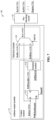
- FIG. 2 illustrates a schematic structural diagram of a refresh control circuit 10 according to an embodiment of the present invention.
- the refresh control circuit 10 is connected with a memory array.
- the refresh control circuit 10 may include: an address output module 11, a block decoding module 121, and a row decoding module 122.
- the address output module 11 is configured to output a to-be-refreshed address signal.
- the to-be-refreshed address signal includes a block address signal and a row address signal.
- the block decoding module 121 is configured to: receive the block address signal; decode the block address signal and output a first block selection signal, in response to that the memory array is subjected to no row hammer attack, or decode the block address signal and output a second block selection signal, in response to that the memory array is subjected to a row hammer attack.
- the first block selection signal is used for selecting multiple data blocks from the memory array
- the second block selection signal is used for selecting one data block from the memory array.
- the row decoding module 122 is configured to receive the row address signal, decode the row address signal, and output a row selection signal.
- the row selection signal is used for selecting a target refresh WL from the one data block selected by the second block selection signal, or selecting target refresh WLs from the multiple data blocks selected by the first block selection signal.
- the refresh control circuit 10 in the embodiments of the present invention is applied to a dynamic memory to solve the problem of relatively high refresh power consumption in the hammer refresh operation.
- the address output module 11 is configured to output the to-be-refreshed address signal
- the to-be-refreshed address signal is configured to indicate a WL address that needs to be refreshed.
- the block decoding module 121 and the row decoding module 122 together form a pre-decoding module 12, and are configured to preliminarily decode the to-be-refreshed address signal to obtain the row selection signal and the block selection signal.
- the row decoding signal and the block decoding signal are configured to enable the target refresh WL after subjecting to subsequent processing.
- the block selection signal includes two types: the first block selection signal and the second block selection signal.
- the block selection signal is the first block selection signal capable of selecting multiple data blocks, so that the corresponding WLs are selected from the multiple data blocks for refresh.
- the block selection signal is the second block selection signal that selects only one data block, so that the corresponding WL is only selected from one data block for refresh, which may reduce the number of the irrelevant WLs being refreshed, reduce the current and power consumption during the hammer refresh process, and improve the performance of the memory.
- the block address signal represents a section obtained by segmenting the bank in a direction of a bit line.
- the upper and lower regions of the address decoding module are both half banks, which together form a complete bank.
- Each half bank may be divided into 8 data blocks. In general refresh, multiple WLs of some sections in the same half bank are refreshed at the same time, and each section generally has at most one WL.
- the actual meaning of the block address represented by the block address signal may be a bank address; in this case, during the general refresh, multiple WLs of some banks of the same chip are refreshed at the same time, and each bank generally has at most one WL.
- the actual meaning represented by the block address signal may include the bank address and the section address; in this case, during the general refresh, the WLs of multiple sections of some banks in the same chip are refreshed at the same time, that is, multiple WLs in any selected bank are refreshed at the same time. All in all, the memory grade represented by the block address signal may be adjusted according to actual needs and subsequent changes in capacity and specifications, and illustrative description is only made herein.
- the specific number of data blocks selected by the first block selection signal may be determined according to an actual application scenario. With the memory array illustrated in FIG. 1 as an example, the first block selection signal selects 4 data blocks each time, which however does not constitute relevant limitation.
- the block decoding module 121 includes: a preprocessing module 21 and a decoding module 22.
- the preprocessing module 21 is configured to receive: a first row hammer signal, a refresh instruction signal and the block address signal; and in response to that the first row hammer signal is invalid, perform first preprocessing on the block address signal based on the refresh instruction signal to obtain a block preselection signal, or in response to that the first row hammer signal is valid, perform second preprocessing based on the block address signal to obtain the block preselection signal.
- the decoding module 22 is configured to receive the block preselection signal, and decode the block preselection signal to obtain the first block selection signal or the second block selection signal.
- the first row hammer signal in response to that the memory array is subjected to no row hammer attack, the first row hammer signal is invalid. In response to that the memory array is subjected to a row hammer attack, the first row hammer signal is valid.
- the refresh instruction signal is configured to instruct execution of the refresh operation.
- the first row hammer signal is used to distinguish this refresh operation as the general refresh operation or the hammer refresh operation, and the first block selection signal or the second block selection signal is obtained by subsequent decoding using a corresponding preprocessing method.
- the number of irrelevant WLs being refreshed in the hammer refresh operation can be reduced without affecting the general refresh operation, and the refresh current and power consumption in the hammer refresh operation can be reduced.
- the block address signal includes a first-type signal and a second-type signal.
- the first-type signal and the second-type signal together form the block address signal.
- the block preselection signal includes a first signal pair and a second signal pair.
- the preprocessing module 21 includes: a first processing module 211 and a second processing module 212.
- the first processing module 211 is configured to receive the first-type signal, perform logical processing on the first-type signal, and output the first signal pair.
- the first signal pair includes the first-type signal and an inverted signal of the first-type signal, and a level state of the first-type signal is opposite to a level state of the inverted signal of the first-type signal.
- the second processing module 212 is configured to receive the first row hammer signal, the refresh instruction signal and the second-type signal; and perform the first preprocessing or the second preprocessing on the second-type signal based on the first row hammer signal and the refresh instruction signal, and output the second signal pair.
- the second signal pair may include the second-type signal and an inverted signal of the second-type signal.
- a level state of the second-type signal is opposite to a level state of the inverted signal of the second-type signal.
- the second-type signal and the inverted signal of the second-type signal are both set to be in a high-level state.
- the to-be-refreshed address signal is composed of 16 sub-signals, which may be expressed as RA ⁇ 15:0>.
- RA ⁇ 15:13> is the block address signal used for selecting the data block; and RA ⁇ 12: 0> is the row address signal used for selecting the WL.
- the first-type signal refers to RA ⁇ 13>, which is processed by the first processing module 211 into the first signal pair (RA13/RA13B).
- the level state of RA13 is the same as that of RA ⁇ 13>, and the level state of RA13B is opposite to that of RA ⁇ 13>.
- the second-type signal refers to RA ⁇ 14> and RA ⁇ 15>, which is processed by the second processing module 212 into a second signal pair (RA14/RA14B, RA15/RA15B).
- the level state of RA14 is the same as that of RA ⁇ 14>
- the level state of RA14B is opposite to that of RA ⁇ 14> are opposite
- the level state of RA15 is the same as that of RA ⁇ 15>
- the level state of RA15B is opposite to that of RA ⁇ 15>.
- RA14, RA14B, RA15, and RA15B are all set to be at a high-level state, and represented to be selected. It is understandable that, in other embodiments, RA14, RA14B, RA15, and RA15B may also be set to represent other selected level states.
- RA13, RA13B, RA14, RA14B, RA15, and RA15B are all synchronized chronologically so as to jointly perform subsequent decoding.
- the first-type signal RA ⁇ 13> and the first-type signal RA13 have the same meaning in a circuit, and therefore they are distinguished only by symbols with no additional name introduced. It is similar for RA ⁇ 14> and RA14, and R.A ⁇ 15> and RA15.
- the number of data blocks and division rules in the memory array may be different, and the number of data blocks that need to be controlled to be enabled is different, then the data bits of the first-type signal and the second-type signal need to be correspondingly adjusted in this case.
- the embodiment of the present invention is only an example but does not constitute a specific limitation.
- the first processing module 211 includes a first NOT gate.
- An input end of the first NOT gate receives the first-type signal RA ⁇ 13>, and an output end of the first NOT gate outputs the inverted signal RA13B of the first-type signal.
- the first processing module 211 may also be provided with a delay device configured to delay the first-type signal RA ⁇ 13>, so as to ensure that the first-type signal RA13 and the inverted signal RA13B of the first-type signal that are synchronous chronologically are obtained.
- the number of the first NOT gate is one.
- the number of the first NOT gates may be multiple, so as to process different first-type signals in parallel.
- only one first NOT gate may be still set; and different first-type signals are processed serially through the delay device, and then another delay device is used to ensure that all first-type signals and the inverted signals of the first-type signals are synchronized chronologically.
- the second processing module 212 includes: an enable module and a logic module.
- the enable module is configured to receive the first row hammer signal RHR and the refresh instruction signal RefreshIP, and output an operation control signal.
- the operation control signal is valid.
- the operation control signal is invalid.
- the logic module is configured to receive the operation control signal and the second-type signal; perform the first preprocessing on the second-type signal and output the second signal pair, in response to that the operation control signal is valid; and perform the second preprocessing on the second-type signal and output the second signal pair, in response to that the operation control signal is invalid.
- the valid first row hammer signal RHR may "disable" the refresh instruction signal RefreshIP to obtain an invalid operation control signal, so that second preprocessing is performed on the second-type signal to obtain the second signal pair, and then a second block decoding signal is obtained by decoding.
- the WL is only selected from one data block for refresh processing, so that the power consumption of hammer refresh is reduced.
- the second processing module 212 may include one enable module and one logic module.
- the enable module and the logic module may process different second-type signals serially, and then ensure that all the second-type signals and the inverted signals of the second-type signals are synchronized chronologically through another delay device.
- the second processing module 212 may include multiple sets of circuits as illustrated in FIG. 5 , each for processing one respective second-type signal.
- the specific composition of the second processing module 212 is exemplarily provided below.
- the enable module includes a second NOT gate 301, a first NAND gate 302 and a third NOT gate 303.
- an input end of the second NOT gate 301 receives the first row hammer signal RHR
- a first input end of the first NAND gate 302 is connected with an output end of the second NOT gate 301
- a second input end of the first NAND gate 302 receives the refresh instruction signal RefreshIP
- an output end of the first NAND gate 302 is connected with the input end of the third NOT gate 303
- an output end of the third NOT gate 303 is configured to output the operation control signal.
- the logic module may include a fourth NOT gate 304, a second NAND gate 305, a fifth NOT gate 306, and a third NAND gate 307.
- the fourth NOT gate 304 receives the operation control signal
- a first input end of the second NAND gate 305 is connected with an output end of the fourth NOT gate 304
- a second input end of the second NAND gate 305 receives the second-type signal
- an output end of the second NAND gate 305 is configured to output the inverted signal of the second-type signal.
- An input end of the fifth NOT gate 306 receives the second-type signal
- a first input end of the third NAND gate 307 is connected with an output end of the fourth NOT gate 304
- a second input end of the third NAND gate 307 is connected with an output end of the fifth NOT gate 306, and an output end of the third NAND gate 307 is configured to output a new second-type signal.
- the operation control signal in response to that the first row hammer signal RHR is valid, the operation control signal is invalid, the level state of RA14B output by the second NAND gate 305 is opposite to that of RA ⁇ 14>, and the level state of RA14 output by the third NAND gate 307 is the same as that of RA ⁇ 14>.
- the operation control signal is valid, and the second NAND gate 305 and the third NAND gate 307 both fixedly output high-level signals, namely RA14B and RA14 are both set to be at a high-level state.
- the block preselection signals RA13, RA13B, RA14, RA14B, RA15 and RA15B are determined by the preprocessing module 21.
- RA14, RA14B, RA15 and RA15B are all set to be at a high-level state.
- the level of none of RA14, RA14B, RA15 and RA15B is forced, so as to accurately select the data block where the victim WL is located, thereby reducing the number of the irrelevant WLs being refreshed in the hammer refresh operation.
- the first block selection signal and the second block selection signal each include multiple block selection sub-signals.
- the multiple block selection sub-signals in the first block selection signal some block selection sub-signals are in a valid state, and the rest block selection sub-signals are in an invalid state, so as to select multiple data blocks from the memory array.
- the multiple block selection sub-signals in the second block selection signal one block selection sub-signal is in a valid state, and the rest block selection sub-signals are in an invalid state, so as to select one data block from the memory array.
- the number of block selection sub-signals in a valid state in the second block selection signal may be controlled to be greater than 1 and smaller than the number of block selection sub-signals in a valid state in the first block selection signal.
- the decoding module 22 includes multiple decoding sub-modules 221 (In FIGS. 3 and 6 , only one decoding sub-module is labeled as an example).
- Each of the multiple decoding sub-modules 221 is configured to receive some signals in the block preselection signal, perform logical operation on the received signals, and output a respective block selection sub-signal (such as Region ⁇ 0>). It is understandable that each of the multiple decoding sub-modules 221 receive respective different signals, and outputs a respective different block selection sub-signal.
- the block selection sub-signal output by the decoding sub-module 221 is in a valid state.
- the preset value may be 1 (high-level signal).
- the decoding sub-module 221 includes a fourth NAND gate and a sixth NOT gate.
- an input end of the fourth NAND gate is configured to receive some signals in the block preselection signal
- an output end of the fourth NAND gate is connected with an input end of the sixth NOT gate
- an output end of the sixth NOT gate is configured to output the block selection sub-signal.
- each decoding sub-module 221 need to be decided according to the actual decoding rule, and FIG. 6 is only an example.
- the address output module 11 is specifically configured to receive a general refresh address signal RefRa ⁇ 15:0> and an activation address signal RaExt ⁇ 15:0>; and in response to that the memory array is subjected to no row hammer attack, output the general refresh address signal RefRa ⁇ 15:0> as the to-be-refreshed address signal RA ⁇ 15:0>, or in response to that the memory array is subjected to a row hammer attack, output the to-be-refreshed address signal RA ⁇ 15:0> based on the activation address signal RaExt ⁇ 15:0>.
- the general refresh address signal RefRa ⁇ 15:0> refers to an address signal in the general refresh operation
- the activation address signal RaExt ⁇ 15:0> refers to an address signal in an activation operation.
- a row hammer attack means that the activation times of a certain WL address in a unit time reaches a threshold value. That is, if the occurrence frequency of the same activation address signal RaExt ⁇ 15:0> in a unit time reaches the threshold value, it is confirmed that the memory array is subjected to a row hammer attack, and the activation address signal RaExt ⁇ 15:0> is also the address signal of the hammer WL.
- the victim WL is the adjacent WL of the hammer WL; therefore, the to-be-refreshed address signal RA ⁇ 15:0> needs to be further determined according to the activation address signal RaExt ⁇ 15:0>.
- the address output module 11 includes: a control module and a selection module 113.
- the control module is configured to receive the activation address signal RaExt ⁇ 15:0>, a second row hammer signal RHRSeedSample and a first control signal RHRRaCtrl; and in response to that the second row hammer signal RHRSeedSample is valid, perform calculation on the activation address signal RaExt ⁇ 15:0> based on the first control signal RHRRaCtrl and output a victim address signal RHRRa ⁇ 15:0>.
- the selection module 113 is configured to receive the general refresh address signal RefRa ⁇ 15:0>, the victim address signal RHRRa ⁇ 15:0> and the second control signal SelCtrl; and in response to that the second control signal SelCtrl is in a first state, output the general refresh address signal RefRa ⁇ 15:0> as the to-be-refreshed address signal RA ⁇ 15:0>, or in response to that the second control signal SelCtrl is in a second state, output the victim address signal RHRRa ⁇ 15:0> as the to-be-refreshed address signal RA ⁇ 15:0>.
- the pre-decoding circuit 12 pre-decodes the to-be-refreshed address signal RA ⁇ 15:0> to obtain the row selection signal (for example, Ra210 ⁇ 7:0>, Ra453 ⁇ 7:0> whilin FIG. 7 ) and the block selection signal Region ⁇ 7:0>, so as to determine the target refresh WL finally.
- the victim address signal RHRRa ⁇ 15:0> is configured to indicate the victim WL in the row hammer attack
- the second row hammer signal RHRSeedSample represents that the memory array is subjected to a row hammer attack
- the first control signal RHRRaCtrl is configured to control the related calculation process.
- the second row hammer signal RHRSeedSample, the first control signal RHRRaCtrl, the second control signal SelCtrl and the aforementioned first row hammer signal RHR are all related to whether the memory array is subjected to a row hammer attack. Since the positions of these signals in the circuit are different, and the timing problem also needs to be considered in determining the change logic thereof, there may be no fixed logical relationship between them.
- the control module includes a latch 111 and a calculation module 112.
- an input end of the latch 111 receives the activation address signal RaExt ⁇ 15:0>
- a clock end of the latch 111 receives the second row hammer signal RHRSeedSample
- an output end of the latch 111 is connected with an input end of the calculation module 112
- a control end of the calculation module 112 receives the first control signal RHRRaCtrl.
- a first input end of the selection module 113 receives the general refresh address signal RefRa ⁇ 15:0>, a second input end of the selection module 113 is connected with an output end of the calculation module 112, a control end of the selection module 113 is connected with the second control signal SelCtrl, and an output end of the selection module 113 is configured to output the to-be-refreshed address signal RA ⁇ 15:0>.
- the latch 111 latches the activation address signal RaExt ⁇ 15:0>, and outputs the hammer address signal RHRSeedRa ⁇ 15:0>.
- the first control signal RHRRaCtrl is valid, and the calculation module 112 calculates the victim address signal RHRRa ⁇ 15:0> according to the hammer address signal RHRSeedRa ⁇ 15:0>.
- the latch 111 is also provided with a reset end, configured to perform a reset operation in response to receiving a reset signal ResetN.
- the activation address signal RaExt ⁇ 15:0> may be the most accessed or relatively more accessed row address signal capable of causing the row hammer effect, or may be the activation address signal newly received after the row hammer effect. In this case, the newly received activation address signal is used as the row address signal causing the row hammer effect.
- the selection module 113 is further provided with a third input end.
- the third input end of the selection module 113 is connected with the activation address signal RaExt ⁇ 15:0>.
- the selection module 113 may output the activation address signal RaExt ⁇ 15:0>, and may perform tasks in some special circumstances.
- valid or “invalid” is distinguished by the level states of the signal.
- a signal being valid may mean that the signal is in a high-level state
- a signal being invalid may mean that the signal is in a low-level state.
- a signal being valid may mean that the signal is in a low-level state
- a signal being invalid may mean that the signal is in a low-level state. This depends on the actual application scenario, as long as it conforms to the corresponding circuit logic and may perform the corresponding circuit function.
- FIG. 8 provides a schematic structural diagram of a second processing module.
- some block selection signals and their inverted signals (RA14, RA14B, RA15, and RA15B) are set to be high-level signals through the refresh instruction signal RefreshIP, so as to select multiple data block, thus facilitating subsequently selecting the target refresh WL from the multiple data blocks for refresh operation.
- RefreshIP refresh instruction signal
- the enable module is added to the second processing module 212, and the first row hammer signal identifying whether the present refresh operation is a hammer refresh operation is introduced.
- the valid first row hammer signal is used to protect the victim WL address, that is, the valid first row hammer signal may Disable the refresh instruction signal RefreshIP, and release the control of the refresh instruction signal RefreshIP on some block selection signals, so that all block selection signals and their inverted signals retain the original control logic, so as to accurately decode the data block where the victim WL is located, only refresh the victim WL, and reduce the current of hammer refresh.
- FIG. 9 illustrates a flowchart of a refresh control method according to an embodiment of present invention. As illustrated in FIG. 9 , the method includes the following operations.
- the to-be-refreshed address signal includes a block address signal and a row address signal.
- the block address signal is decoded to obtain a first block selection signal, in response to that a memory array is subjected to no row hammer attack.
- the block address signal is decoded to obtain a second block selection signal, in response to that the memory array is subjected to a row hammer attack.
- the first block selection signal may be used for selecting multiple data blocks from the memory array
- the second block selection signal may be used for selecting one data block from the memory array.
- the row address signal is decoded to obtain a row selection signal.
- the row selection signal may be used for selecting a target refresh WL from the one data block selected by the second block selection signal, or selecting target refresh WLs from the multiple data blocks selected by the first block selection signal.
- the target refresh WL is refreshed.
- the refresh control method provided by the embodiment of the present invention is applied to the aforementioned refresh control circuit 10, and the refresh control circuit 10 is connected with the memory array.
- the target refresh WL is selected from only one data block for refresh processing, which can reduce the number of irrelevant WLs being refreshed, reduce the refresh current and power consumption during the hammer refresh process, and improve the performance of a memory.
- S402 may specifically include the following operations.
- a first row hammer signal and a refresh instruction signal are determined.
- the first row hammer signal in response to that the memory array is subjected to no row hammer attack, the first row hammer signal is invalid.
- the first row hammer signal is valid.
- first preprocessing is performed on the block address signal based on the refresh instruction signal to obtain a block preselection signal; or in response to that the first row hammer signal is valid, second preprocessing is performed based on the block address signal to obtain the block preselection signal.
- the block preselection signal is decoded to obtain the first block selection signal or the second block selection signal.
- the block address signal includes a first-type signal and a second-type signal.
- the block preselection signal includes a first signal pair and a second signal pair.
- the first signal pair includes the first-type signal and an inverted signal of the first-type signal, and a level state of the first-type signal is opposite to a level state of the inverted signal of the first-type signal.
- the second signal pair includes the second-type signal and an inverted signal of the second-type signal.
- a level state of the second-type signal is opposite to a level state of the inverted signal of the second-type signal.
- the second-type signal and the inverted signal of the second-type signal are both set to be in a high-level state.
- the first block selection signal and the second block selection signal each include multiple block selection sub-signals.
- the multiple block selection sub-signals in the first block selection signal some block selection sub-signals are in a valid state, and the rest block selection sub-signals are in an invalid state, so as to select multiple data blocks from the memory array.
- the multiple block selection sub-signals in the second block selection signal one block selection sub-signal is in a valid state, and the rest block selection sub-signals are in an invalid state, so as to select one data block from the memory array.
- the operation that the to-be-refreshed address signal is determined includes the following operations.
- a general refresh address signal and an activation address signal are received.
- the general refresh address signal is output as the to-be-refreshed address signal; or in response to that the memory array is subjected to a row hammer attack, the to-be-refreshed address signal is output based on the activation address signal.
- the activation address signal is configured to indicate the attacked WL in the row hammer attack
- the to-be-refreshed address signal is configured to indicate the victim WL in the row hammer attack. Therefore, in this scenario, the to-be-refreshed address signal needs to be calculated according to the activation address signal.
- the embodiments of the present invention provide the refresh control method.
- the target refresh WL is selected from only one data block for refresh processing, which can reduce the number of irrelevant WLs being refreshed, reduce the refresh current and power consumption during the hammer refresh process, and improve the performance of the memory.
- FIG. 10 illustrates a schematic structural diagram of a memory 50 according to an embodiment of present invention.
- the memory 50 includes aforementioned refresh control circuit 10 and a memory array 501.
- the refresh control circuit 10 is connected with the memory array 501.
- the refresh control circuit 10 may select a target refresh WL from only one data block for refresh processing, which can reduce the number of irrelevant WLs refreshed, reduce the current and power consumption during the hammer refresh process, and improve the performance of the memory.
- the embodiments of the present invention provide a refresh control circuit and method, and a memory, which can reduce the number of irrelevant WLs being refreshed in a hammer refresh operation and reduce refresh current and power consumption, thereby improving the performance of the memory.
Landscapes
- Engineering & Computer Science (AREA)
- Microelectronics & Electronic Packaging (AREA)
- Computer Hardware Design (AREA)
- Dram (AREA)
Abstract
Description
- The application is based upon and claims priority to
Chinese Patent Application No. 202210724803.6, filed on June 23, 2022 - The present invention relates to the technical field of semiconductor memories, in particular to a refresh control circuit and method, and a memory.
- Row Hammer attacks are a kind of data attacks directed at a Dynamic Random Access Memory (DRAM), which cause data loss of adjacent Word Lines (WLs) (hereinafter referred to as victim WL) by frequently refreshing a certain WL (hereinafter referred to as hammer WL) in a short time. At present, when a row hammer attack is detected, the victim WLs need to be refreshed to recover the affected data, also known as a hammer refresh operation. However, the hammer refresh operation needs to be implemented by means of a general refresh operation process, which causes some irrelevant WLs to be additionally refreshed during the hammer refresh process, resulting in a waste of resources and reducing the performance of the memory.
- The present invention provides a refresh control circuit and method, and a memory, which can reduce the number of irrelevant word lines (WLs) being refreshed in a hammer refresh operation and reduce refresh current and power consumption.
- The technical solutions of the present invention are implemented as follows.
- In a first aspect, embodiments of the present invention provide a refresh control circuit. The refresh control circuit is connected with a memory array and includes:
an address output module, a block decoding module, and a row decoding module. - The address output module may be configured to output a to-be-refreshed address signal. The to-be-refreshed address signal includes a block address signal and a row address signal. The block decoding module is configured to receive the block address signal, decode the block address signal and output a first block selection signal, in response to that the memory array is subjected to no row hammer attack, or decode the block address signal and output a second block selection signal, in response to that the memory array is subjected to a row hammer attack. Herein, the first block selection signal is used for selecting multiple data blocks from the memory array, and the second block selection signal is used for selecting one data block from the memory array. The row decoding module may be configured to receive the row address signal, decode the row address signal, and output a row selection signal. The row selection signal is used for selecting a target refresh word line (WL) from the one data block selected by the second block selection signal, or selecting target refresh WLs from the multiple data blocks selected by the first block selection signal.
- In some embodiments, the block decoding module may include: a preprocessing module, configured to receive a first row hammer signal, a refresh instruction signal and the block address signal; in response to that the first row hammer signal is invalid, perform first preprocessing on the block address signal based on the refresh instruction signal to obtain a block preselection signal, or in response to that the first row hammer signal is valid, perform second preprocessing based on the block address signal to obtain the block preselection signal; and a decoding module, configured to receive the block preselection signal, and decode the block preselection signal to obtain the first block selection signal or the second block selection signal. Herein, in response to that the memory array is subjected to no row hammer attack, the first row hammer signal is invalid; and in response to that the memory array is subjected to a row hammer attack, the first row hammer signal is valid.
- In some embodiments, the block address signal may include a first-type signal and a second-type signal. The block preselection signal may include a first signal pair and a second signal pair. The preprocessing module may include: a first processing module and a second processing module. The first processing module may be configured to receive the first-type signal, perform logical processing on the first-type signal, and output the first signal pair. Herein, the first signal pair may include the first-type signal and an inverted signal of the first-type signal, and a level state of the first-type signal is opposite to a level state of the inverted signal of the first-type signal. The second processing module may be configured to receive the first row hammer signal, the refresh instruction signal and the second-type signal; and perform the first preprocessing or the second preprocessing on the second-type signal based on the first row hammer signal and the refresh instruction signal, and output the second signal pair. Herein, the second signal pair may include the second-type signal and an inverted signal of the second-type signal. In response to that the first row hammer signal is valid, a level state of the second-type signal is opposite to a level state of the inverted signal of the second-type signal are opposite; and in response to that the first row hammer signal is invalid and the refresh instruction signal is valid, the second-type signal and the inverted signal of the second-type signal are both set to be in a high-level state.
- In some embodiments, the first processing module may include a first NOT gate. An input end of the first NOT gate receives the first-type signal, and an output end of the first NOT gate outputs the inverted signal of the first-type signal.
- In some embodiments, the second processing module may include: an enable module and a logic module. The enable module may be configured to receive the first row hammer signal and the refresh instruction signal, and output an operation control signal. Herein, in response to that the first row hammer signal is invalid and the refresh instruction signal is valid, the operation control signal is valid. In response to that the first row hammer signal is valid, the operation control signal is invalid. The logic module may be configured to receive the operation control signal and the second-type signal; perform the first preprocessing on the second-type signal and output the second signal pair, in response to that the operation control signal is valid; and perform the second preprocessing on the second-type signal and output the second signal pair, in response to that the operation control signal is invalid.
- In some embodiments, the enable module may include a second NOT gate, a first NAND gate and a third NOT gate. Herein, an input end of the second NOT gate receives the first row hammer signal, a first input end of the first NAND gate is connected with an output end of the second NOT gate, a second input end of the first NAND gate receives the refresh instruction signal, an output end of the first NAND gate is connected with the input end of the third NOT gate, and an output end of the third NOT gate is configured to output the operation control signal.
- In some embodiments, the logic module may include a fourth NOT gate, a second NAND gate, a fifth NOT gate, and a third NAND gate. Herein, the fourth NOT gate receives the operation control signal, a first input end of the second NAND gate is connected with an output end of the fourth NOT gate, a second input end of the second NAND gate receives the second-type signal, and an output end of the second NAND gate is configured to output the inverted signal of the second-type signal. An input end of the fifth NOT gate receives the second-type signal, a first input end of the third NAND gate is connected with an output end of the fourth NOT gate, a second input end of the third NAND gate is connected with an output end of the fifth NOT gate, and an output end of the third NAND gate is configured to output a new second-type signal.
- In some embodiments, the first block selection signal and the second block selection signal each include multiple block selection sub-signals. Among the multiple block selection sub-signals in the first block selection signal, some block selection sub-signals are in a valid state, and the rest block selection sub-signals are in an invalid state, so as to select multiple data blocks from the memory array. Among the multiple block selection sub-signals in the second block selection signal, one block selection sub-signal is in a valid state, and the rest block selection sub-signals are in an invalid state, so as to select one data block from the memory array.
- In some embodiments, the decoding module may include multiple decoding sub-modules. Each of the multiple decoding sub-modules is configured to receive some signals in the block preselection signal, perform logical operation on the received signals, and output a respective block selection sub-signal. Each of the multiple decoding sub-modules receives respective different signals. Herein, in response to that a result of the logic operation is a preset value, the block selection sub-signal output by the decoding sub-module is in a valid state.
- In some embodiments, the address output module is configured to receive a general refresh address signal and an activation address signal; and in response to that the memory array is subjected to no row hammer attack, output the general refresh address signal as the to-be-refreshed address signal, or in response to that the memory array is subjected to a row hammer attack, output the to-be-refreshed address signal based on the activation address signal.
- In some embodiments, the address output module may include: a control module, configured to receive the activation address signal, a second row hammer signal and a first control signal; and in response to that the second row hammer signal is valid, perform calculation on the activation address signal based on the first control signal and output a victim address signal; and a selection module, configured to receive the general refresh address signal, the victim address signal and the second control signal; and in response to that the second control signal is in a first state, output the general refresh address signal as the to-be-refreshed address signal, or in response to that the second control signal is in a second state, output the victim address signal as the to-be-refreshed address signal. Herein, the second row hammer signal represents that the memory array is subjected to a row hammer attack.
- In some embodiments, the control module may include a latch and a calculation module. Herein, an input end of the latch receives the activation address signal, a clock end of the latch receives the second row hammer signal, an output end of the latch is connected with an input end of the calculation module, and a control end of the calculation module receives the first control signal. A first input end of the selection module receives the general refresh address signal, a second input end of the selection module is connected with an output end of the calculation module, a control end of the selection module is connected with the second control signal, and an output end of the selection module is configured to output the to-be-refreshed address signal.
- In a second aspect, the embodiments of the present invention provide a refresh control method, which is applied to a refresh control circuit and connected with a memory array. The method may include the following operations.
- A to-be-refreshed address signal is determined. The to-be-refreshed address signal includes a block address signal and a row address signal. The block address signal is decoded to obtain a first block selection signal, in response to that the memory array is subjected to no row hammer attack. The block address signal is decoded to obtain a second block selection signal, in response to that the memory array is subjected to a row hammer attack. Herein, the first block selection signal may be used for selecting multiple data blocks from the memory array, and the second block selection signal may be used for selecting one data block from the memory array. The row address signal is decoded to obtain a row selection signal. The row selection signal is used for selecting a target refresh word line (WL) from the one data block selected by the second block selection signal, or selecting target refresh WLs from the multiple data blocks selected by the first block selection signal. The target refresh WL(s) is (are) refreshed.
- In a third aspect, the embodiments of the present invention provide a memory, which may include a refresh control circuit as described in a first aspect and a memory array. The refresh control circuit is connected with the memory array.
- The embodiments of the present invention provide a refresh control circuit and method, and a memory, which can reduce the number of irrelevant WLs being refreshed in a hammer refresh operation and reduce refresh current and power consumption, thereby improving the performance of the memory.
-
-
FIG. 1 illustrates a schematic structural diagram of a memory array. -
FIG. 2 illustrates a schematic structural diagram of a refresh control circuit according to an embodiment of present invention. -
FIG. 3 illustrates a schematic structural diagram of a block decoding module according to an embodiment of present invention. -
FIG. 4 illustrates a schematic structural diagram of a first processing module according to an embodiment of present invention. -
FIG. 5 illustrates a schematic structural diagram of a second processing module according to an embodiment of present invention. -
FIG. 6 illustrates a schematic structural diagram of a decoding module according to an embodiment of present invention. -
FIG. 7 illustrates a schematic structural diagram of another refresh control circuit according to an embodiment of present invention. -
FIG. 8 illustrates a schematic structural diagram of a second processing module according to the related art. -
FIG. 9 illustrates a flowchart of a refresh control method according to an embodiment of present invention. -
FIG. 10 illustrates a schematic structural diagram of a memory according to an embodiment of present invention. - The technical solutions in the embodiments of the present invention will be clearly and completely described in conjunction with the drawings in the embodiments of the present invention. It is understandable that the specific embodiments described herein are only used to illustrate the relevant disclosure, but are not intended to limit the present invention. In addition, it is to be noted that, for the convenience of description, only the parts related to the relevant disclosure are shown in the drawings. Unless otherwise defined, all technical and scientific terms used herein have the same meaning as commonly understood by those skilled in the art of the present invention. The terms used herein are only for the purpose of describing the embodiments of the present invention and are not intended to limit the present invention. In the following description, reference is made to "some embodiments" which describe a subset of all possible embodiments, but it is understandable that "some embodiments" may be the same or different subsets of all possible embodiments, and may be combined with each other without conflict. It is to be noted that the terms "first\second\third" involved in the embodiments of the present invention are only used to distinguish similar objects, and do not represent a specific order of the objects. It is understandable that the specific order or sequence of "first\second\third" may be interchangeable under the allowable circumstances, so that the embodiments of the present invention described herein may be implemented in an order other than those illustrated or described herein.
- A DRAM needs to maintain data in a memory cell through a refresh operation. In a general refresh operation, each refresh operation may enable multiple data blocks in a memory array, and a WL is further selected from the enabled data blocks for refresh processing. Referring to
FIG. 1, FIG. 1 illustrates a schematic structural diagram of a memory array. As illustrated inFIG. 1 , the memory array is divided into: adata block 0, adata block 1......adata block 7. An address signal in the refresh operation may be expressed as RA<15:0>. Herein, RA<15:13> is a block address signal used for selecting the data block that needs to be enabled. RA<12:0> is a row address signal used for selecting a target refresh WL from the enabled data block. In a general refresh operation, RA14, RA14B, RA15, and RA15B are all forced to be at a high level, where "B" represents an inverted signal. Since "RA14=0" is represented as "RA14=1" in circuit decoding, it may be considered that RA14=1, RA14=0, RA15=1, and RA15=0 are all valid. Taking R.A<15:13>=000 as an example, since thedata block 0, thedata block 2, thedata block 4 and the data block 6 all use Ra13B as a block preselection signal, and Ra14 and Ra15 and their inverted signals are forced to 1, the data block is actually only selected based on Ra13. Since the even stages of data blocks (the data blocks 0, 2, 4, and 6) use Ra13B, when Ra13=0, the even stages of data blocks are selected. That is, in the general refresh operation, the corresponding WLs (decoded by RA<12:0>) are selected from 4 data blocks for refresh each time. In particular, in memory arrays with different storage capacities, the number of data blocks and the decoding process may be different; in this case, the number of selected data blocks is also different.FIG. 1 is only an example. - However, when a row hammer attack is detected, a Victim WL needs to be refreshed to restore the affected data, and hammer refresh needs to be implemented by means of the general refresh process. Taking
FIG. 1 as an example, it is assumed that the victim WL is a WL in thedata block 0, but due to the aforementioned decoding mechanism, thedata block 0, thedata block 2, thedata block 4 and the data block 6 are still all selected, rendering that some irrelevant WLs of the memory may also be refreshed additionally during the hammer refresh process, resulting in a waste of resources and reducing the performance of the memory. - The embodiments of the present invention provide a refresh control circuit, which may reduce the number of irrelevant WLs being refreshed in a hammer refresh operation and reduce refresh current and power consumption, thereby improving the performance of the memory.
- The embodiments of the present invention will be described in detail below with reference to the accompanying drawings.
- In an embodiment of the present invention, referring to
FIG. 2, FIG. 2 illustrates a schematic structural diagram of arefresh control circuit 10 according to an embodiment of the present invention. Therefresh control circuit 10 is connected with a memory array. As illustrated inFIG. 2 , therefresh control circuit 10 may include: anaddress output module 11, ablock decoding module 121, and arow decoding module 122. - The
address output module 11 is configured to output a to-be-refreshed address signal. The to-be-refreshed address signal includes a block address signal and a row address signal. - The
block decoding module 121 is configured to: receive the block address signal; decode the block address signal and output a first block selection signal, in response to that the memory array is subjected to no row hammer attack, or decode the block address signal and output a second block selection signal, in response to that the memory array is subjected to a row hammer attack. Herein, the first block selection signal is used for selecting multiple data blocks from the memory array, and the second block selection signal is used for selecting one data block from the memory array. - The
row decoding module 122 is configured to receive the row address signal, decode the row address signal, and output a row selection signal. The row selection signal is used for selecting a target refresh WL from the one data block selected by the second block selection signal, or selecting target refresh WLs from the multiple data blocks selected by the first block selection signal. - It is to be noted that, the
refresh control circuit 10 in the embodiments of the present invention is applied to a dynamic memory to solve the problem of relatively high refresh power consumption in the hammer refresh operation. - Here, the
address output module 11 is configured to output the to-be-refreshed address signal, and the to-be-refreshed address signal is configured to indicate a WL address that needs to be refreshed. Theblock decoding module 121 and therow decoding module 122 together form apre-decoding module 12, and are configured to preliminarily decode the to-be-refreshed address signal to obtain the row selection signal and the block selection signal. The row decoding signal and the block decoding signal are configured to enable the target refresh WL after subjecting to subsequent processing. - In the embodiments of the present invention, the block selection signal includes two types: the first block selection signal and the second block selection signal. In the general refresh operation (that is, the memory array is subjected to no row hammer attack), the block selection signal is the first block selection signal capable of selecting multiple data blocks, so that the corresponding WLs are selected from the multiple data blocks for refresh. In the hammer refresh operation (that is, the memory array is subjected to a row hammer attack), the block selection signal is the second block selection signal that selects only one data block, so that the corresponding WL is only selected from one data block for refresh, which may reduce the number of the irrelevant WLs being refreshed, reduce the current and power consumption during the hammer refresh process, and improve the performance of the memory.
- It is to be noted that the actual meaning of a block address represented by the block address signal may be adjusted according to the actual situation. Specifically, when a selection object is a certain bank or a half bank, the block address signal represents a section obtained by segmenting the bank in a direction of a bit line. As illustrated in
FIG. 1 , the upper and lower regions of the address decoding module are both half banks, which together form a complete bank. Each half bank may be divided into 8 data blocks. In general refresh, multiple WLs of some sections in the same half bank are refreshed at the same time, and each section generally has at most one WL. When the selection object is the entire chip, the actual meaning of the block address represented by the block address signal may be a bank address; in this case, during the general refresh, multiple WLs of some banks of the same chip are refreshed at the same time, and each bank generally has at most one WL. Further, when the selection object is the entire chip, the actual meaning represented by the block address signal may include the bank address and the section address; in this case, during the general refresh, the WLs of multiple sections of some banks in the same chip are refreshed at the same time, that is, multiple WLs in any selected bank are refreshed at the same time. All in all, the memory grade represented by the block address signal may be adjusted according to actual needs and subsequent changes in capacity and specifications, and illustrative description is only made herein. - It is to be noted that the specific number of data blocks selected by the first block selection signal may be determined according to an actual application scenario. With the memory array illustrated in
FIG. 1 as an example, the first block selection signal selects 4 data blocks each time, which however does not constitute relevant limitation. - In some embodiments, as illustrated in
FIG. 3 , theblock decoding module 121 includes: a preprocessingmodule 21 and adecoding module 22. - The
preprocessing module 21 is configured to receive: a first row hammer signal, a refresh instruction signal and the block address signal; and in response to that the first row hammer signal is invalid, perform first preprocessing on the block address signal based on the refresh instruction signal to obtain a block preselection signal, or in response to that the first row hammer signal is valid, perform second preprocessing based on the block address signal to obtain the block preselection signal. - The
decoding module 22 is configured to receive the block preselection signal, and decode the block preselection signal to obtain the first block selection signal or the second block selection signal. - It is to be noted that, in response to that the memory array is subjected to no row hammer attack, the first row hammer signal is invalid. In response to that the memory array is subjected to a row hammer attack, the first row hammer signal is valid. In addition, the refresh instruction signal is configured to instruct execution of the refresh operation.
- In this way, the first row hammer signal is used to distinguish this refresh operation as the general refresh operation or the hammer refresh operation, and the first block selection signal or the second block selection signal is obtained by subsequent decoding using a corresponding preprocessing method. The number of irrelevant WLs being refreshed in the hammer refresh operation can be reduced without affecting the general refresh operation, and the refresh current and power consumption in the hammer refresh operation can be reduced.
- In some embodiments, the block address signal includes a first-type signal and a second-type signal. The first-type signal and the second-type signal together form the block address signal. The block preselection signal includes a first signal pair and a second signal pair. As illustrated in
FIG. 3 , thepreprocessing module 21 includes: afirst processing module 211 and asecond processing module 212. - The
first processing module 211 is configured to receive the first-type signal, perform logical processing on the first-type signal, and output the first signal pair. Herein, the first signal pair includes the first-type signal and an inverted signal of the first-type signal, and a level state of the first-type signal is opposite to a level state of the inverted signal of the first-type signal. - The
second processing module 212 is configured to receive the first row hammer signal, the refresh instruction signal and the second-type signal; and perform the first preprocessing or the second preprocessing on the second-type signal based on the first row hammer signal and the refresh instruction signal, and output the second signal pair. Herein, the second signal pair may include the second-type signal and an inverted signal of the second-type signal. In response to that the first row hammer signal is valid, a level state of the second-type signal is opposite to a level state of the inverted signal of the second-type signal. In response to that the first row hammer signal is invalid and the refresh instruction signal is valid, the second-type signal and the inverted signal of the second-type signal are both set to be in a high-level state. - A specific example is provided below to describe the decoding process of the to-be-refreshed address signal in detail. In the example, the to-be-refreshed address signal is composed of 16 sub-signals, which may be expressed as RA<15:0>. Herein, RA<15:13> is the block address signal used for selecting the data block; and RA<12: 0> is the row address signal used for selecting the WL.
- Referring to
FIG. 1 , the first-type signal refers to RA<13>, which is processed by thefirst processing module 211 into the first signal pair (RA13/RA13B). At this time, the level state of RA13 is the same as that of RA<13>, and the level state of RA13B is opposite to that of RA<13>. - The second-type signal refers to RA<14> and RA<15>, which is processed by the
second processing module 212 into a second signal pair (RA14/RA14B, RA15/RA15B). In the hammer refresh operation, the level state of RA14 is the same as that of RA<14>, the level state of RA14B is opposite to that of RA<14> are opposite, the level state of RA15 is the same as that of RA<15>, and the level state of RA15B is opposite to that of RA<15>. In the general refresh operation, RA14, RA14B, RA15, and RA15B are all set to be at a high-level state, and represented to be selected. It is understandable that, in other embodiments, RA14, RA14B, RA15, and RA15B may also be set to represent other selected level states. - In particular, RA13, RA13B, RA14, RA14B, RA15, and RA15B are all synchronized chronologically so as to jointly perform subsequent decoding.
- It is understandable that the first-type signal RA<13> and the first-type signal RA13 have the same meaning in a circuit, and therefore they are distinguished only by symbols with no additional name introduced. It is similar for RA<14> and RA14, and R.A<15> and RA15. In addition, in memories with different storage capacities, the number of data blocks and division rules in the memory array may be different, and the number of data blocks that need to be controlled to be enabled is different, then the data bits of the first-type signal and the second-type signal need to be correspondingly adjusted in this case. The embodiment of the present invention is only an example but does not constitute a specific limitation.
- In some embodiments, as illustrated in
FIG. 4 , thefirst processing module 211 includes a first NOT gate. An input end of the first NOT gate receives the first-type signal RA<13>, and an output end of the first NOT gate outputs the inverted signal RA13B of the first-type signal. - It is to be noted that, the
first processing module 211 may also be provided with a delay device configured to delay the first-type signal RA<13>, so as to ensure that the first-type signal RA13 and the inverted signal RA13B of the first-type signal that are synchronous chronologically are obtained. - It is also to be noted that there is only one first-type signal in
FIG. 4 , and therefore the number of the first NOT gate is one. In a case where there are multiple first-type signals, the number of the first NOT gates may be multiple, so as to process different first-type signals in parallel. Alternatively, in a case where there are multiple first-type signals, only one first NOT gate may be still set; and different first-type signals are processed serially through the delay device, and then another delay device is used to ensure that all first-type signals and the inverted signals of the first-type signals are synchronized chronologically. - In some embodiments, as illustrated in
FIG. 5 , thesecond processing module 212 includes: an enable module and a logic module. - The enable module is configured to receive the first row hammer signal RHR and the refresh instruction signal RefreshIP, and output an operation control signal. Herein, in response to that the first row hammer signal RHR is invalid and the refresh instruction signal RefreshIP is valid, the operation control signal is valid. In response to that the first row hammer signal RHR is valid, the operation control signal is invalid.
- The logic module is configured to receive the operation control signal and the second-type signal; perform the first preprocessing on the second-type signal and output the second signal pair, in response to that the operation control signal is valid; and perform the second preprocessing on the second-type signal and output the second signal pair, in response to that the operation control signal is invalid.
- That is, when the memory array is subjected to a row hammer attack, the valid first row hammer signal RHR may "disable" the refresh instruction signal RefreshIP to obtain an invalid operation control signal, so that second preprocessing is performed on the second-type signal to obtain the second signal pair, and then a second block decoding signal is obtained by decoding. The WL is only selected from one data block for refresh processing, so that the power consumption of hammer refresh is reduced.
- Similarly, in a case where there is one second-type signal, the
second processing module 212 may include one enable module and one logic module. In a case where there are multiple second-type signals, as illustrated inFIG. 5 , the enable module and the logic module may process different second-type signals serially, and then ensure that all the second-type signals and the inverted signals of the second-type signals are synchronized chronologically through another delay device. Alternatively, in a case where there are multiple second-type signals, thesecond processing module 212 may include multiple sets of circuits as illustrated inFIG. 5 , each for processing one respective second-type signal. - Due to the diversity of circuit devices, there are various possibilities for the specific composition of the second processing module, as long as the aforementioned circuit logic can be implemented. The specific composition of the
second processing module 212 is exemplarily provided below. - In some embodiments, the enable module includes a
second NOT gate 301, afirst NAND gate 302 and athird NOT gate 303. Herein, an input end of thesecond NOT gate 301 receives the first row hammer signal RHR, a first input end of thefirst NAND gate 302 is connected with an output end of thesecond NOT gate 301, a second input end of thefirst NAND gate 302 receives the refresh instruction signal RefreshIP, an output end of thefirst NAND gate 302 is connected with the input end of thethird NOT gate 303, and an output end of thethird NOT gate 303 is configured to output the operation control signal. - In some embodiments, as illustrated in
FIG. 5 , the logic module may include afourth NOT gate 304, asecond NAND gate 305, afifth NOT gate 306, and athird NAND gate 307. Herein, thefourth NOT gate 304 receives the operation control signal, a first input end of thesecond NAND gate 305 is connected with an output end of thefourth NOT gate 304, a second input end of thesecond NAND gate 305 receives the second-type signal, and an output end of thesecond NAND gate 305 is configured to output the inverted signal of the second-type signal. An input end of thefifth NOT gate 306 receives the second-type signal, a first input end of thethird NAND gate 307 is connected with an output end of thefourth NOT gate 304, a second input end of thethird NAND gate 307 is connected with an output end of thefifth NOT gate 306, and an output end of thethird NAND gate 307 is configured to output a new second-type signal. - It is to be noted that, taking the second-type signal RA<14> as an example, in response to that the first row hammer signal RHR is valid, the operation control signal is invalid, the level state of RA14B output by the
second NAND gate 305 is opposite to that of RA<14>, and the level state of RA14 output by thethird NAND gate 307 is the same as that of RA<14>. In response to that the first row hammer signal RHR is invalid and the refresh instruction signal RefreshIP is valid, the operation control signal is valid, and thesecond NAND gate 305 and thethird NAND gate 307 both fixedly output high-level signals, namely RA14B and RA14 are both set to be at a high-level state. - In this way, the block preselection signals RA13, RA13B, RA14, RA14B, RA15 and RA15B are determined by the
preprocessing module 21. In the general refresh operation, RA14, RA14B, RA15 and RA15B are all set to be at a high-level state. In the hammer refresh operation, the level of none of RA14, RA14B, RA15 and RA15B is forced, so as to accurately select the data block where the victim WL is located, thereby reducing the number of the irrelevant WLs being refreshed in the hammer refresh operation. - In some embodiments, the first block selection signal and the second block selection signal each include multiple block selection sub-signals. Among the multiple block selection sub-signals in the first block selection signal, some block selection sub-signals are in a valid state, and the rest block selection sub-signals are in an invalid state, so as to select multiple data blocks from the memory array. Among the multiple block selection sub-signals in the second block selection signal, one block selection sub-signal is in a valid state, and the rest block selection sub-signals are in an invalid state, so as to select one data block from the memory array. In other embodiments, the number of block selection sub-signals in a valid state in the second block selection signal may be controlled to be greater than 1 and smaller than the number of block selection sub-signals in a valid state in the first block selection signal.
- Exemplarily, the number of block selection sub-signals may be 8; in this case, the first block selection signal and the second block selection signal may be both represented as Region<7:0>. Correspondingly, as illustrated in
FIGS. 3 and6 , thedecoding module 22 includes multiple decoding sub-modules 221 (InFIGS. 3 and6 , only one decoding sub-module is labeled as an example). Each of themultiple decoding sub-modules 221 is configured to receive some signals in the block preselection signal, perform logical operation on the received signals, and output a respective block selection sub-signal (such as Region<0>). It is understandable that each of themultiple decoding sub-modules 221 receive respective different signals, and outputs a respective different block selection sub-signal. - Herein, in response to that a result of the logic operation is a preset value, the block selection sub-signal output by the
decoding sub-module 221 is in a valid state. Exemplarily, the preset value may be 1 (high-level signal). - In some embodiments, as illustrated in
FIG. 6 , thedecoding sub-module 221 includes a fourth NAND gate and a sixth NOT gate. Herein, an input end of the fourth NAND gate is configured to receive some signals in the block preselection signal, an output end of the fourth NAND gate is connected with an input end of the sixth NOT gate, and an output end of the sixth NOT gate is configured to output the block selection sub-signal. - It is to be noted that the specific signals received by each
decoding sub-module 221 need to be decided according to the actual decoding rule, andFIG. 6 is only an example. Assuming that R.A<15:13>=000, in the absence of row hammer attacks, RA15=RA15B=RA14=RA14B=1, RA13=0, RA13B=1. In this case, Region<0>=Region<2> =Region<4>=Region<6>=1 (equivalent to a valid state), that is, thedata block 0, thedata block 2, thedata block 4, and the data block 6 are selected. In a case of a row hammer attack, RA15=0, RA15B=1, RA14=0, RA14B=1, RA13=0, RA13B=1; in this case, only Region<0>=l, that is, only the data block 0 is selected. It can be seen that through a calibration control circuit provided by the embodiments of the present invention, only the data block where the victim WL is located can be selected for the refresh operation during the hammer refresh, so that the refresh of irrelevant WLs and power consumption are reduced. - In some embodiments, as illustrated in
FIG. 7 , theaddress output module 11 is specifically configured to receive a general refresh address signal RefRa<15:0> and an activation address signal RaExt<15:0>; and in response to that the memory array is subjected to no row hammer attack, output the general refresh address signal RefRa<15:0> as the to-be-refreshed address signal RA<15:0>, or in response to that the memory array is subjected to a row hammer attack, output the to-be-refreshed address signal RA<15:0> based on the activation address signal RaExt<15:0>. - It is to be noted that, the general refresh address signal RefRa<15:0> refers to an address signal in the general refresh operation, and the activation address signal RaExt<15:0> refers to an address signal in an activation operation. It is understandable that a row hammer attack means that the activation times of a certain WL address in a unit time reaches a threshold value. That is, if the occurrence frequency of the same activation address signal RaExt<15:0> in a unit time reaches the threshold value, it is confirmed that the memory array is subjected to a row hammer attack, and the activation address signal RaExt<15:0> is also the address signal of the hammer WL. In particular, in the row hammer attack scenario, the victim WL is the adjacent WL of the hammer WL; therefore, the to-be-refreshed address signal RA<15:0> needs to be further determined according to the activation address signal RaExt<15:0>.
- In some embodiments, as illustrated in
FIG. 7 , theaddress output module 11 includes: a control module and aselection module 113. - The control module is configured to receive the activation address signal RaExt<15:0>, a second row hammer signal RHRSeedSample and a first control signal RHRRaCtrl; and in response to that the second row hammer signal RHRSeedSample is valid, perform calculation on the activation address signal RaExt<15:0> based on the first control signal RHRRaCtrl and output a victim address signal RHRRa<15:0>.
- The
selection module 113 is configured to receive the general refresh address signal RefRa<15:0>, the victim address signal RHRRa<15:0> and the second control signal SelCtrl; and in response to that the second control signal SelCtrl is in a first state, output the general refresh address signal RefRa<15:0> as the to-be-refreshed address signal RA<15:0>, or in response to that the second control signal SelCtrl is in a second state, output the victim address signal RHRRa<15:0> as the to-be-refreshed address signal RA<15:0>. In addition, thepre-decoding circuit 12 pre-decodes the to-be-refreshed address signal RA<15:0> to obtain the row selection signal (for example, Ra210<7:0>, Ra453<7:0>......inFIG. 7 ) and the block selection signal Region<7:0>, so as to determine the target refresh WL finally. - Here, the victim address signal RHRRa<15:0> is configured to indicate the victim WL in the row hammer attack, the second row hammer signal RHRSeedSample represents that the memory array is subjected to a row hammer attack, and the first control signal RHRRaCtrl is configured to control the related calculation process. In particular, the second row hammer signal RHRSeedSample, the first control signal RHRRaCtrl, the second control signal SelCtrl and the aforementioned first row hammer signal RHR are all related to whether the memory array is subjected to a row hammer attack. Since the positions of these signals in the circuit are different, and the timing problem also needs to be considered in determining the change logic thereof, there may be no fixed logical relationship between them.
- In some embodiments, the control module includes a
latch 111 and acalculation module 112. Herein, an input end of thelatch 111 receives the activation address signal RaExt<15:0>, a clock end of thelatch 111 receives the second row hammer signal RHRSeedSample, an output end of thelatch 111 is connected with an input end of thecalculation module 112, and a control end of thecalculation module 112 receives the first control signal RHRRaCtrl. A first input end of theselection module 113 receives the general refresh address signal RefRa<15:0>, a second input end of theselection module 113 is connected with an output end of thecalculation module 112, a control end of theselection module 113 is connected with the second control signal SelCtrl, and an output end of theselection module 113 is configured to output the to-be-refreshed address signal RA<15:0>. - In this way, in a case where the second row hammer signal RHRSeedSample is valid, the
latch 111 latches the activation address signal RaExt<15:0>, and outputs the hammer address signal RHRSeedRa<15:0>. At the same time, the first control signal RHRRaCtrl is valid, and thecalculation module 112 calculates the victim address signal RHRRa<15:0> according to the hammer address signal RHRSeedRa<15:0>. Here, thelatch 111 is also provided with a reset end, configured to perform a reset operation in response to receiving a reset signal ResetN. - It is to be noted that, the activation address signal RaExt<15:0> may be the most accessed or relatively more accessed row address signal capable of causing the row hammer effect, or may be the activation address signal newly received after the row hammer effect. In this case, the newly received activation address signal is used as the row address signal causing the row hammer effect.
- In addition, as illustrated in
FIG. 7 , theselection module 113 is further provided with a third input end. The third input end of theselection module 113 is connected with the activation address signal RaExt<15:0>. Correspondingly, in response to that the second control signal SelCtrl is in a third state, theselection module 113 may output the activation address signal RaExt<15:0>, and may perform tasks in some special circumstances. - In the embodiments of the present invention, "valid" or "invalid" is distinguished by the level states of the signal. For example, a signal being valid may mean that the signal is in a high-level state, and a signal being invalid may mean that the signal is in a low-level state. Alternatively, a signal being valid may mean that the signal is in a low-level state, and a signal being invalid may mean that the signal is in a low-level state. This depends on the actual application scenario, as long as it conforms to the corresponding circuit logic and may perform the corresponding circuit function.
- To sum up, the embodiments of the present invention provide a refresh control circuit, which can select only the data block where the victim WL is located in the hammer refresh operation, thereby reducing the current and power consumption of the hammer refresh. Referring to
FIG. 8, FIG. 8 provides a schematic structural diagram of a second processing module. As illustrated inFIG. 8 , some block selection signals and their inverted signals (RA14, RA14B, RA15, and RA15B) are set to be high-level signals through the refresh instruction signal RefreshIP, so as to select multiple data block, thus facilitating subsequently selecting the target refresh WL from the multiple data blocks for refresh operation. In the embodiments of the present invention, as illustrated inFIG. 5 , the enable module is added to thesecond processing module 212, and the first row hammer signal identifying whether the present refresh operation is a hammer refresh operation is introduced. The valid first row hammer signal is used to protect the victim WL address, that is, the valid first row hammer signal may Disable the refresh instruction signal RefreshIP, and release the control of the refresh instruction signal RefreshIP on some block selection signals, so that all block selection signals and their inverted signals retain the original control logic, so as to accurately decode the data block where the victim WL is located, only refresh the victim WL, and reduce the current of hammer refresh. - In another embodiment of the present invention, referring to
FIG. 9, FIG. 9 illustrates a flowchart of a refresh control method according to an embodiment of present invention. As illustrated inFIG. 9 , the method includes the following operations. - At S401, a to-be-refreshed address signal is determined. The to-be-refreshed address signal includes a block address signal and a row address signal.
- At S402, the block address signal is decoded to obtain a first block selection signal, in response to that a memory array is subjected to no row hammer attack. The block address signal is decoded to obtain a second block selection signal, in response to that the memory array is subjected to a row hammer attack. Herein, the first block selection signal may be used for selecting multiple data blocks from the memory array, and the second block selection signal may be used for selecting one data block from the memory array.
- At S403, the row address signal is decoded to obtain a row selection signal. The row selection signal may be used for selecting a target refresh WL from the one data block selected by the second block selection signal, or selecting target refresh WLs from the multiple data blocks selected by the first block selection signal.
- At S404, the target refresh WL is refreshed.
- It is to be noted that the refresh control method provided by the embodiment of the present invention is applied to the aforementioned
refresh control circuit 10, and therefresh control circuit 10 is connected with the memory array. In this way, in a case where the memory array is subjected to a row hammer attack, the target refresh WL is selected from only one data block for refresh processing, which can reduce the number of irrelevant WLs being refreshed, reduce the refresh current and power consumption during the hammer refresh process, and improve the performance of a memory. - In some embodiments, S402 may specifically include the following operations.
- A first row hammer signal and a refresh instruction signal are determined. Herein, in response to that the memory array is subjected to no row hammer attack, the first row hammer signal is invalid. In response to that the memory array is subjected to a row hammer attack, the first row hammer signal is valid. In response to that the first row hammer signal is invalid, first preprocessing is performed on the block address signal based on the refresh instruction signal to obtain a block preselection signal; or in response to that the first row hammer signal is valid, second preprocessing is performed based on the block address signal to obtain the block preselection signal. The block preselection signal is decoded to obtain the first block selection signal or the second block selection signal.
- In some embodiments, the block address signal includes a first-type signal and a second-type signal. The block preselection signal includes a first signal pair and a second signal pair. Herein, (1) the first signal pair includes the first-type signal and an inverted signal of the first-type signal, and a level state of the first-type signal is opposite to a level state of the inverted signal of the first-type signal. (2) The second signal pair includes the second-type signal and an inverted signal of the second-type signal. In response to that the first row hammer signal is valid, a level state of the second-type signal is opposite to a level state of the inverted signal of the second-type signal. In response to that the first row hammer signal is invalid and the refresh instruction signal is valid, the second-type signal and the inverted signal of the second-type signal are both set to be in a high-level state.
- In some embodiments, the first block selection signal and the second block selection signal each include multiple block selection sub-signals. Among the multiple block selection sub-signals in the first block selection signal, some block selection sub-signals are in a valid state, and the rest block selection sub-signals are in an invalid state, so as to select multiple data blocks from the memory array. Among the multiple block selection sub-signals in the second block selection signal, one block selection sub-signal is in a valid state, and the rest block selection sub-signals are in an invalid state, so as to select one data block from the memory array.
- In some embodiments, the operation that the to-be-refreshed address signal is determined includes the following operations.
- A general refresh address signal and an activation address signal are received. In response to that the memory array is subjected to no row hammer attack, the general refresh address signal is output as the to-be-refreshed address signal; or in response to that the memory array is subjected to a row hammer attack, the to-be-refreshed address signal is output based on the activation address signal.
- It is to be noted that, when the memory array is subjected to a row hammer attack, the activation address signal is configured to indicate the attacked WL in the row hammer attack, and the to-be-refreshed address signal is configured to indicate the victim WL in the row hammer attack. Therefore, in this scenario, the to-be-refreshed address signal needs to be calculated according to the activation address signal.
- The embodiments of the present invention provide the refresh control method. In a case where the memory array is subjected to a row hammer attack, the target refresh WL is selected from only one data block for refresh processing, which can reduce the number of irrelevant WLs being refreshed, reduce the refresh current and power consumption during the hammer refresh process, and improve the performance of the memory.
- In another embodiment of the present invention, referring to
FIG. 10, FIG. 10 illustrates a schematic structural diagram of amemory 50 according to an embodiment of present invention. As illustrated inFIG. 10 , thememory 50 includes aforementionedrefresh control circuit 10 and amemory array 501. Therefresh control circuit 10 is connected with thememory array 501. - For the
memory 50, in response to that the memory array is subjected to a row hammer attack, therefresh control circuit 10 may select a target refresh WL from only one data block for refresh processing, which can reduce the number of irrelevant WLs refreshed, reduce the current and power consumption during the hammer refresh process, and improve the performance of the memory. - The above are only preferred embodiments of the present invention, and are not intended to limit the scope of protection of the present invention. It is to be noted that in this disclosure, the terms "comprise/comprising", "include/including", "contain/containing" or any other variations thereof are intended to cover non-exclusive inclusion, so that a process, method, article or device including a series of elements includes not only those elements, but also other elements not explicitly listed, or elements inherent to the process, method, article or device. Without more restrictions, an element defined by the sentence "comprising/including a ..." does not exclude the existence of other identical elements in the process, method, article, or device including the element. The above numbers of the embodiments of the present invention are only for description, and do not represent the advantages or disadvantages of the embodiments. The methods disclosed in the several method embodiments provided in the present invention may be combined arbitrarily without conflict to obtain new method embodiments. The features disclosed in the several product embodiments provided in the present invention may be combined arbitrarily without conflict to obtain new product embodiment. The features disclosed in several method or device embodiments provided in the present invention may be combined arbitrarily without conflict to obtain new method embodiments or device embodiments. The above are only detailed description of the present invention and are not intended to limit the scope of protection of the present invention. Any variation or replacement apparent to those skilled in the art within the technical scope disclosed by the invention shall fall within the scope of protection of the present invention. Therefore, the scope of protection of the present invention shall be subject to the scope of protection of the claims.
- The embodiments of the present invention provide a refresh control circuit and method, and a memory, which can reduce the number of irrelevant WLs being refreshed in a hammer refresh operation and reduce refresh current and power consumption, thereby improving the performance of the memory.
Claims (14)
- A refresh control circuit, connected with a memory array and comprising:an address output module, configured to output a to-be-refreshed address signal, the to-be-refreshed address signal comprising a block address signal and a row address signal;a block decoding module, configured to: receive the block address signal; and decode the block address signal and output a first block selection signal, in response to that the memory array is subjected to no row hammer attack, or decode the block address signal and output a second block selection signal, in response to that the memory array is subjected to a row hammer attack; wherein the first block selection signal is used for selecting multiple data blocks from the memory array, and the second block selection signal is used for selecting one data block from the memory array; anda row decoding module, configured to receive the row address signal, decode the row address signal, and output a row selection signal, wherein the row selection signal is used for selecting a target refresh word line (WL) from the one data block selected by the second block selection signal, or selecting target refresh WLs from the multiple data blocks selected by the first block selection signal.
- The refresh control circuit of claim 1, wherein the block decoding module comprises:a preprocessing module, configured to receive a first row hammer signal, a refresh instruction signal and the block address signal; in response to that the first row hammer signal is invalid, perform first preprocessing on the block address signal based on the refresh instruction signal to obtain a block preselection signal, or in response to that the first row hammer signal is valid, perform second preprocessing based on the block address signal to obtain the block preselection signal; anda decoding module, configured to receive the block preselection signal, and decode the block preselection signal to obtain the first block selection signal or the second block selection signal;wherein in response to that the memory array is subjected to no row hammer attack, the first row hammer signal is invalid; and in response to that the memory array is subjected to a row hammer attack, the first row hammer signal is valid.
- The refresh control circuit of claim 2, wherein the block address signal comprises a first-type signal and a second-type signal, and the block preselection signal comprises a first signal pair and a second signal pair; and
the preprocessing module comprises:a first processing module, configured to receive the first-type signal, perform logical processing on the first-type signal, and output the first signal pair; wherein the first signal pair comprises the first-type signal and an inverted signal of the first-type signal, and a level state of the first-type signal is opposite to a level state of the inverted signal of the first-type signal; anda second processing module, configured to receive the first row hammer signal, the refresh instruction signal and the second-type signal; and perform the first preprocessing or the second preprocessing on the second-type signal based on the first row hammer signal and the refresh instruction signal, and output the second signal pair;wherein the second signal pair comprises the second-type signal and an inverted signal of the second-type signal; in response to that the first row hammer signal is valid, a level state of the second-type signal is opposite to a level state of the inverted signal of the second-type signal are opposite; and in response to that the first row hammer signal is invalid and the refresh instruction signal is valid, the second-type signal and the inverted signal of the second-type signal are both set to be in a high-level state. - The refresh control circuit of claim 3, wherein the first processing module comprises a first NOT gate, an input end of the first NOT gate receives the first-type signal, and an output end of the first NOT gate outputs the inverted signal of the first-type signal.
- The refresh control circuit of claim 3, wherein the second processing module comprises:an enable module, configured to receive the first row hammer signal and the refresh instruction signal, and output an operation control signal; wherein in response to that the first row hammer signal is invalid and the refresh instruction signal is valid, the operation control signal is valid, and in response to that the first row hammer signal is valid, the operation control signal is invalid; anda logic module, configured to receive the operation control signal and the second-type signal; perform the first preprocessing on the second-type signal and output the second signal pair, in response to that the operation control signal is valid; and perform the second preprocessing on the second-type signal and output the second signal pair, in response to that the operation control signal is invalid.
- The refresh control circuit of claim 5, wherein the enable module comprises a second NOT gate, a first NAND gate and a third NOT gate; and
an input end of the second NOT gate receives the first row hammer signal, a first input end of the first NAND gate is connected with an output end of the second NOT gate, a second input end of the first NAND gate receives the refresh instruction signal, an output end of the first NAND gate is connected with the input end of the third NOT gate, and an output end of the third NOT gate is configured to output the operation control signal. - The refresh control circuit of claim 5, wherein the logic module comprises a fourth NOT gate, a second NAND gate, a fifth NOT gate, and a third NAND gate;the fourth NOT gate receives the operation control signal, a first input end of the second NAND gate is connected with an output end of the fourth NOT gate, a second input end of the second NAND gate receives the second-type signal, and an output end of the second NAND gate is configured to output the inverted signal of the second-type signal; andan input end of the fifth NOT gate receives the second-type signal, a first input end of the third NAND gate is connected with an output end of the fourth NOT gate, a second input end of the third NAND gate is connected with an output end of the fifth NOT gate, and an output end of the third NAND gate is configured to output a new second-type signal.
- The refresh control circuit of claim 2, wherein the first block selection signal and the second block selection signal each comprise multiple block selection sub-signals;among the multiple block selection sub-signals in the first block selection signal, some block selection sub-signals are in a valid state, and the rest block selection sub-signals are in an invalid state, so as to select multiple data blocks from the memory array; andamong the multiple block selection sub-signals in the second block selection signal, one block selection sub-signal is in a valid state, and the rest block selection sub-signals are in an invalid state, so as to select one data block from the memory array.
- The refresh control circuit of claim 8, wherein the decoding module comprises multiple decoding sub-modules;each of the multiple decoding sub-modules is configured to receive some signals in the block preselection signal, perform logical operation on the received signals, and output a respective block selection sub-signal, wherein each of the multiple decoding sub-modules receives respective different signals;wherein in response to that a result of the logic operation is a preset value, the block selection sub-signal output by the decoding sub-module is in a valid state.
- The refresh control circuit of claim 1, wherein:
the address output module is configured to receive a general refresh address signal and an activation address signal; and in response to that the memory array is subjected to no row hammer attack, output the general refresh address signal as the to-be-refreshed address signal, or in response to that the memory array is subjected to a row hammer attack, output the to-be-refreshed address signal based on the activation address signal. - The refresh control circuit of claim 10, wherein the address output module comprises:a control module, configured to receive the activation address signal, a second row hammer signal and a first control signal; and in response to that the second row hammer signal is valid, perform calculation on the activation address signal based on the first control signal and output a victim address signal; anda selection module, configured to receive the general refresh address signal, the victim address signal and the second control signal; and in response to that the second control signal is in a first state, output the general refresh address signal as the to-be-refreshed address signal, or in response to that the second control signal is in a second state, output the victim address signal as the to-be-refreshed address signal;wherein the second row hammer signal represents that the memory array is subjected to a row hammer attack.
- The refresh control circuit of claim 11, wherein the control module comprises a latch and a calculation module; whereinan input end of the latch receives the activation address signal, a clock end of the latch receives the second row hammer signal, an output end of the latch is connected with an input end of the calculation module, and a control end of the calculation module receives the first control signal; anda first input end of the selection module receives the general refresh address signal, a second input end of the selection module is connected with an output end of the calculation module, a control end of the selection module is connected with the second control signal, and an output end of the selection module is configured to output the to-be-refreshed address signal.
- A refresh control method, applied to a refresh control circuit and connected with a memory array, and comprising:determining a to-be-refreshed address signal, the to-be-refreshed address signal comprising a block address signal and a row address signal;decoding the block address signal to obtain a first block selection signal in response to that the memory array is subjected to no row hammer attack; and decoding the block address signal to obtain a second block selection signal in response to that the memory array is subjected to a row hammer attack; wherein the first block selection signal is used for selecting multiple data blocks from the memory array, and the second block selection signal is used for selecting one data block from the memory array;decoding the row address signal to obtain a row selection signal, wherein the row selection signal is used for selecting a target refresh word line (WL) from the one data block selected by the second block selection signal, or selecting target refresh WLs from the multiple data blocks selected by the first block selection signal; andrefreshing the target refresh WL(s).
- A memory, comprising a refresh control circuit of any one of claims 1-12 and a memory array, the refresh control circuit being connected with the memory array.
Applications Claiming Priority (2)
| Application Number | Priority Date | Filing Date | Title |
|---|---|---|---|
| CN202210724803.6A CN117316224A (en) | 2022-06-23 | 2022-06-23 | Refresh control circuit and method, memory |
| PCT/CN2022/107097 WO2023245792A1 (en) | 2022-06-23 | 2022-07-21 | Refresh control circuit and method therefor, and memory |
Publications (2)
| Publication Number | Publication Date |
|---|---|
| EP4325498A1 true EP4325498A1 (en) | 2024-02-21 |
| EP4325498A4 EP4325498A4 (en) | 2024-06-26 |
Family
ID=84046063
Family Applications (1)
| Application Number | Title | Priority Date | Filing Date |
|---|---|---|---|
| EP22834833.0A Withdrawn EP4325498A4 (en) | 2022-06-23 | 2022-07-21 | COOLING CONTROL CIRCUIT AND ASSOCIATED METHOD, AND MEMORY |
Country Status (4)
| Country | Link |
|---|---|
| US (1) | US12119039B2 (en) |
| EP (1) | EP4325498A4 (en) |
| JP (1) | JP7543430B2 (en) |
| KR (1) | KR102803084B1 (en) |
Families Citing this family (1)
| Publication number | Priority date | Publication date | Assignee | Title |
|---|---|---|---|---|
| US12265731B2 (en) * | 2023-07-13 | 2025-04-01 | Qualcomm Incorporated | Partial row refresh in a memory device |
Family Cites Families (23)
| Publication number | Priority date | Publication date | Assignee | Title |
|---|---|---|---|---|
| US6469947B2 (en) | 1999-06-29 | 2002-10-22 | Hyundai Electronics Co., Ltd. | Semiconductor memory device having regions with independent word lines alternately selected for refresh operation |
| US8284615B2 (en) | 2010-12-28 | 2012-10-09 | Hynix Semiconductor Inc. | Refresh control circuit and method for semiconductor memory device |
| US8284614B2 (en) | 2010-12-28 | 2012-10-09 | Hynix Semiconductor Inc. | Refresh control circuit and method for semiconductor memory device |
| KR102020905B1 (en) * | 2012-04-10 | 2019-09-11 | 삼성전자주식회사 | Method for caring address accessed frequently and memory system with address caring function |
| US8938573B2 (en) | 2012-06-30 | 2015-01-20 | Intel Corporation | Row hammer condition monitoring |
| US9236110B2 (en) | 2012-06-30 | 2016-01-12 | Intel Corporation | Row hammer refresh command |
| US9384821B2 (en) | 2012-11-30 | 2016-07-05 | Intel Corporation | Row hammer monitoring based on stored row hammer threshold value |
| US9324398B2 (en) | 2013-02-04 | 2016-04-26 | Micron Technology, Inc. | Apparatuses and methods for targeted refreshing of memory |
| US9269436B2 (en) | 2013-03-12 | 2016-02-23 | Intel Corporation | Techniques for determining victim row addresses in a volatile memory |
| WO2014142254A1 (en) * | 2013-03-15 | 2014-09-18 | ピーエスフォー ルクスコ エスエイアールエル | Semiconductor storage device and system provided with same |
| JP2015219938A (en) | 2014-05-21 | 2015-12-07 | マイクロン テクノロジー, インク. | Semiconductor device |
| KR20160035444A (en) | 2014-09-23 | 2016-03-31 | 에스케이하이닉스 주식회사 | Smart refresh device |
| KR102315277B1 (en) * | 2014-11-03 | 2021-10-20 | 삼성전자 주식회사 | Semiconductor Memory Device with Improved Refresh Characteristics |
| US10497409B2 (en) | 2014-12-17 | 2019-12-03 | International Business Machines Corporation | Implementing DRAM row hammer avoidance |
| KR102468251B1 (en) | 2016-06-27 | 2022-11-18 | 에스케이하이닉스 주식회사 | Semiconductor memory device and operating method thereof |
| JP6576480B2 (en) | 2018-01-16 | 2019-09-18 | 華邦電子股▲ふん▼有限公司Winbond Electronics Corp. | Memory device and data refresh method thereof |
| KR20190123875A (en) | 2018-04-25 | 2019-11-04 | 삼성전자주식회사 | Semiconductor memory device and memory system having the same |
| US11152050B2 (en) | 2018-06-19 | 2021-10-19 | Micron Technology, Inc. | Apparatuses and methods for multiple row hammer refresh address sequences |
| CN113168861B (en) * | 2018-12-03 | 2024-05-14 | 美光科技公司 | Semiconductor device performing row hammer refresh operation |
| US10943637B2 (en) * | 2018-12-27 | 2021-03-09 | Micron Technology, Inc. | Apparatus with a row-hammer address latch mechanism |
| US10950288B2 (en) | 2019-03-29 | 2021-03-16 | Intel Corporation | Refresh command control for host assist of row hammer mitigation |
| US11302376B2 (en) | 2020-08-25 | 2022-04-12 | Micron Technology, Inc. | Systems and methods for memory refresh |
| CN114649023A (en) | 2022-03-23 | 2022-06-21 | 长鑫存储技术有限公司 | Address selection circuit, control method thereof and memory |
-
2022
- 2022-07-21 KR KR1020227037846A patent/KR102803084B1/en active Active
- 2022-07-21 JP JP2022562394A patent/JP7543430B2/en active Active
- 2022-07-21 EP EP22834833.0A patent/EP4325498A4/en not_active Withdrawn
- 2022-09-27 US US17/935,746 patent/US12119039B2/en active Active
Also Published As
| Publication number | Publication date |
|---|---|
| KR20220152336A (en) | 2022-11-15 |
| KR102803084B1 (en) | 2025-05-07 |
| JP2024526390A (en) | 2024-07-18 |
| EP4325498A4 (en) | 2024-06-26 |
| JP7543430B2 (en) | 2024-09-02 |
| US20230420026A1 (en) | 2023-12-28 |
| US12119039B2 (en) | 2024-10-15 |
Similar Documents
| Publication | Publication Date | Title |
|---|---|---|
| US9792975B1 (en) | Dram and access and operating method thereof | |
| US11972828B2 (en) | Repair circuit, memory, and repair method | |
| US9653181B1 (en) | Smart self-repair device and method of self-repairing a package | |
| US11854653B2 (en) | Signal masking circuit and semiconductor memory | |
| EP3896693B1 (en) | Memory and addressing method therefor | |
| US12119039B2 (en) | Refresh control circuit and method, and memory | |
| CN109841259B (en) | Method and device for improving NOR type memory array reading speed | |
| US9208856B2 (en) | Multiport memory with matching address control | |
| TWI855511B (en) | Refresh control circuit and method, and memory | |
| US9601216B2 (en) | Semiconductor device including redundancy cell array | |
| US6988164B1 (en) | Compare circuit and method for content addressable memory (CAM) device | |
| US6075733A (en) | Technique for reducing peak current in memory operation | |
| KR100618858B1 (en) | A semiconductor memory device capable of varying the number of banks to be refreshed when performing a refresh and a refresh method thereof | |
| WO2023103148A1 (en) | Address refresh circuit, method, memory, and electronic device | |
| EP4276832A1 (en) | Address refresh circuit, method, memory, and electronic device | |
| US12119037B2 (en) | Refresh circuit, memory, and refresh method | |
| CN116741220B (en) | A refresh circuit, memory and refresh method | |
| US12136450B2 (en) | Memory and operation method of memory with repairing and random pulse generating capability | |
| US6567324B2 (en) | Semiconductor memory device with reduced number of redundant program sets | |
| US20230221892A1 (en) | Memory interface | |
| KR100715525B1 (en) | Multi-port memory device with independent input and output power and clock | |
| WO2024016426A1 (en) | Method and apparatus for testing memory chip, device, and storage medium | |
| KR100754361B1 (en) | Multi-port memory device capable of sharing data I / O power | |
| CN117636938A (en) | Refresh control circuit and method thereof, semiconductor memory | |
| US7813213B1 (en) | Pulsed arbitration system |
Legal Events
| Date | Code | Title | Description |
|---|---|---|---|
| STAA | Information on the status of an ep patent application or granted ep patent |
Free format text: STATUS: UNKNOWN |
|
| STAA | Information on the status of an ep patent application or granted ep patent |
Free format text: STATUS: THE INTERNATIONAL PUBLICATION HAS BEEN MADE |
|
| PUAI | Public reference made under article 153(3) epc to a published international application that has entered the european phase |
Free format text: ORIGINAL CODE: 0009012 |
|
| STAA | Information on the status of an ep patent application or granted ep patent |
Free format text: STATUS: REQUEST FOR EXAMINATION WAS MADE |
|
| 17P | Request for examination filed |
Effective date: 20230110 |
|
| AK | Designated contracting states |
Kind code of ref document: A1 Designated state(s): AL AT BE BG CH CY CZ DE DK EE ES FI FR GB GR HR HU IE IS IT LI LT LU LV MC MK MT NL NO PL PT RO RS SE SI SK SM TR |
|
| A4 | Supplementary search report drawn up and despatched |
Effective date: 20240528 |
|
| RIC1 | Information provided on ipc code assigned before grant |
Ipc: G11C 11/408 20060101ALI20240522BHEP Ipc: G11C 11/406 20060101AFI20240522BHEP |
|
| STAA | Information on the status of an ep patent application or granted ep patent |
Free format text: STATUS: THE APPLICATION IS DEEMED TO BE WITHDRAWN |
|
| 18D | Application deemed to be withdrawn |
Effective date: 20241217 |