EP4322219A1 - Semiconductor structure and preparation method therefor, and memory and preparation method therefor - Google Patents
Semiconductor structure and preparation method therefor, and memory and preparation method therefor Download PDFInfo
- Publication number
- EP4322219A1 EP4322219A1 EP22783273.0A EP22783273A EP4322219A1 EP 4322219 A1 EP4322219 A1 EP 4322219A1 EP 22783273 A EP22783273 A EP 22783273A EP 4322219 A1 EP4322219 A1 EP 4322219A1
- Authority
- EP
- European Patent Office
- Prior art keywords
- active pillars
- chips
- active
- chip
- substrate
- Prior art date
- Legal status (The legal status is an assumption and is not a legal conclusion. Google has not performed a legal analysis and makes no representation as to the accuracy of the status listed.)
- Granted
Links
Images




Classifications
-
- H—ELECTRICITY
- H10—SEMICONDUCTOR DEVICES; ELECTRIC SOLID-STATE DEVICES NOT OTHERWISE PROVIDED FOR
- H10B—ELECTRONIC MEMORY DEVICES
- H10B12/00—Dynamic random access memory [DRAM] devices
- H10B12/01—Manufacture or treatment
- H10B12/02—Manufacture or treatment for one transistor one-capacitor [1T-1C] memory cells
- H10B12/03—Making the capacitor or connections thereto
- H10B12/036—Making the capacitor or connections thereto the capacitor extending under the transistor
-
- H—ELECTRICITY
- H10—SEMICONDUCTOR DEVICES; ELECTRIC SOLID-STATE DEVICES NOT OTHERWISE PROVIDED FOR
- H10B—ELECTRONIC MEMORY DEVICES
- H10B12/00—Dynamic random access memory [DRAM] devices
- H10B12/01—Manufacture or treatment
- H10B12/02—Manufacture or treatment for one transistor one-capacitor [1T-1C] memory cells
- H10B12/03—Making the capacitor or connections thereto
- H10B12/038—Making the capacitor or connections thereto the capacitor being in a trench in the substrate
- H10B12/0383—Making the capacitor or connections thereto the capacitor being in a trench in the substrate wherein the transistor is vertical
-
- H—ELECTRICITY
- H10—SEMICONDUCTOR DEVICES; ELECTRIC SOLID-STATE DEVICES NOT OTHERWISE PROVIDED FOR
- H10D—INORGANIC ELECTRIC SEMICONDUCTOR DEVICES
- H10D1/00—Resistors, capacitors or inductors
- H10D1/60—Capacitors
- H10D1/62—Capacitors having potential barriers
- H10D1/66—Conductor-insulator-semiconductor capacitors, e.g. MOS capacitors
- H10D1/665—Trench conductor-insulator-semiconductor capacitors, e.g. trench MOS capacitors
-
- H—ELECTRICITY
- H10—SEMICONDUCTOR DEVICES; ELECTRIC SOLID-STATE DEVICES NOT OTHERWISE PROVIDED FOR
- H10W—GENERIC PACKAGES, INTERCONNECTIONS, CONNECTORS OR OTHER CONSTRUCTIONAL DETAILS OF DEVICES COVERED BY CLASS H10
- H10W72/00—Interconnections or connectors in packages
- H10W72/90—Bond pads, in general
-
- H—ELECTRICITY
- H10—SEMICONDUCTOR DEVICES; ELECTRIC SOLID-STATE DEVICES NOT OTHERWISE PROVIDED FOR
- H10W—GENERIC PACKAGES, INTERCONNECTIONS, CONNECTORS OR OTHER CONSTRUCTIONAL DETAILS OF DEVICES COVERED BY CLASS H10
- H10W80/00—Direct bonding of chips, wafers or substrates
-
- H—ELECTRICITY
- H10—SEMICONDUCTOR DEVICES; ELECTRIC SOLID-STATE DEVICES NOT OTHERWISE PROVIDED FOR
- H10W—GENERIC PACKAGES, INTERCONNECTIONS, CONNECTORS OR OTHER CONSTRUCTIONAL DETAILS OF DEVICES COVERED BY CLASS H10
- H10W90/00—Package configurations
-
- H—ELECTRICITY
- H10—SEMICONDUCTOR DEVICES; ELECTRIC SOLID-STATE DEVICES NOT OTHERWISE PROVIDED FOR
- H10W—GENERIC PACKAGES, INTERCONNECTIONS, CONNECTORS OR OTHER CONSTRUCTIONAL DETAILS OF DEVICES COVERED BY CLASS H10
- H10W99/00—Subject matter not provided for in other groups of this subclass
-
- H—ELECTRICITY
- H10—SEMICONDUCTOR DEVICES; ELECTRIC SOLID-STATE DEVICES NOT OTHERWISE PROVIDED FOR
- H10W—GENERIC PACKAGES, INTERCONNECTIONS, CONNECTORS OR OTHER CONSTRUCTIONAL DETAILS OF DEVICES COVERED BY CLASS H10
- H10W72/00—Interconnections or connectors in packages
- H10W72/01—Manufacture or treatment
- H10W72/0198—Manufacture or treatment batch processes
-
- H—ELECTRICITY
- H10—SEMICONDUCTOR DEVICES; ELECTRIC SOLID-STATE DEVICES NOT OTHERWISE PROVIDED FOR
- H10W—GENERIC PACKAGES, INTERCONNECTIONS, CONNECTORS OR OTHER CONSTRUCTIONAL DETAILS OF DEVICES COVERED BY CLASS H10
- H10W90/00—Package configurations
- H10W90/20—Configurations of stacked chips
- H10W90/28—Configurations of stacked chips the stacked chips having different sizes, e.g. chip stacks having a pyramidal shape
-
- H—ELECTRICITY
- H10—SEMICONDUCTOR DEVICES; ELECTRIC SOLID-STATE DEVICES NOT OTHERWISE PROVIDED FOR
- H10W—GENERIC PACKAGES, INTERCONNECTIONS, CONNECTORS OR OTHER CONSTRUCTIONAL DETAILS OF DEVICES COVERED BY CLASS H10
- H10W90/00—Package configurations
- H10W90/701—Package configurations characterised by the relative positions of pads or connectors relative to package parts
- H10W90/751—Package configurations characterised by the relative positions of pads or connectors relative to package parts of bond wires
- H10W90/754—Package configurations characterised by the relative positions of pads or connectors relative to package parts of bond wires between a chip and a stacked insulating package substrate, interposer or RDL
Definitions
- the application relates to the technical field of semiconductors, and in particular to a semiconductor structure, a method for manufacturing a semiconductor structure, a memory, and a method for manufacturing a memory.
- a memory for example, a Dynamic Random Access Memory, DRAM usually includes a memory array circuit and a peripheral circuit.
- the memory array circuit generally consists of a plurality of memory cells arranged in an array.
- the memory cell generally consists of a transistor and a capacitor.
- An embodiment of the application provides a semiconductor structure, which includes: a substrate; a plurality of capacitors arranged in the substrate; and a plurality of active pillars arranged above the substrate.
- Each of the plurality of active pillars is arranged above a respective one of the plurality of capacitors, and a bottom portion of each of the plurality of active pillars is electrically connected to a top portion of the respective one of the plurality of capacitors therebelow.
- the semiconductor structure further includes: a plurality of word lines extending in a first direction, in which the plurality of word lines are arranged above the substrate, and each of the plurality of word lines is arranged around a sidewall of a respective one of the plurality of active pillars; and a plurality of bit lines extending in a second direction which intersects with the first direction, in which the plurality of bit lines are arranged above the plurality of active pillars, and a bottom portion of each of the plurality of bit lines are electrically connected to top portions of the plurality of active pillars.
- the semiconductor structure further includes: a dielectric layer arranged above the substrate and covering the sidewalls of the plurality of active pillars; a lower filling layer filled in gaps between any two adjacent active pillars of the plurality of active pillars below the plurality of word lines; and an upper filling layer filled in gaps between any two adjacent word lines of the plurality of word lines and gaps between any two adjacent active pillars of the plurality of active pillars above the plurality of word lines.
- the semiconductor structure further includes a contact.
- the contact penetrates through the upper filling layer and the lower filling layer.
- a bottom portion of the contact is electrically connected to the plurality of capacitors.
- a material of each of the plurality of active pillars comprises indium gallium zinc oxide.
- An embodiment of the application provides a memory, which includes: a first chip including the semiconductor structure described in any one of the above embodiments; and a second chip including a peripheral circuit. An active surface of the first chip is bumplessly bonded to an active surface of the second chip.
- the second chip is arranged below the first chip.
- a projection of the second chip in a vertical direction covers a projection of the first chip in the vertical direction.
- the memory further includes a base plate arranged below the second chip.
- a projection of the base plate in the vertical direction covers the projection of the second chip in the vertical direction.
- the base plate is bonded to the second chip through a lead wire.
- An embodiment of the application further provides a method for manufacturing a semiconductor structure, which includes the following operations.
- a substrate is provided.
- a plurality of capacitors are formed in the substrate.
- a plurality of active pillars are formed above the substrate, in which each of the plurality of active pillars is arranged above a respective one of the plurality of capacitors, and a bottom portion of each of the plurality of active pillars is electrically connected to a top portion of the respective one of the plurality of capacitors therebelow.
- the method further includes the following operations.
- a plurality of word lines extending in a first direction are formed, in which the plurality of word lines are arranged above the substrate, and each of the plurality of word lines is arranged around a sidewall of a respective one of the plurality of active pillars.
- a plurality of bit lines extending in a second direction which intersects with the first direction are formed, in which the plurality of bit lines are arranged above the plurality of active pillars, and a bottom portion of each of the plurality of bit lines is electrically connected to top portions of the plurality of active pillars.
- the method before the plurality of bit lines are formed, the method further includes the following operation.
- a contact is formed, in which a bottom portion of the contact is electrically connected to the plurality of capacitors.
- the operation that the plurality of capacitors are formed includes the following operations.
- a mask layer is deposited above the substrate.
- the mask layer and the substrate are patterned to form a plurality of grooves.
- a capacitor lower electrode, a capacitor dielectric layer and a capacitor upper electrode are sequentially formed in each of the plurality of grooves.
- the operation that the plurality of active pillars are formed includes the following operations.
- a semiconductor layer is formed above the plurality of capacitors.
- the semiconductor layer is patterned to form the plurality of active pillars, in which each of the plurality of active pillars is arranged above the respective one of the plurality of capacitors.
- the operation that the plurality of word lines are formed includes the following operations.
- a dielectric layer is formed, in which the dielectric layer covers the plurality of active pillars.
- a lower filling layer is formed, in which the lower filling layer is partially filled in gaps between any two adjacent active pillars of the plurality of active pillars, and exposes a channel area in each of the plurality of active pillars.
- a word line material layer is formed on the lower filling layer, and the word line material layer is etched in the first direction to form the plurality of word lines extending in the first direction, in which each of the plurality of word lines is arranged around the channel area in a respective one of the plurality of active pillars.
- An upper filling layer is formed.
- Planarization is performed to remove the dielectric layer covering the top portions of the plurality of active pillars and to remove the upper filling layer covering the top portions of the plurality of active pillars, so as to allow a surface of the upper filling layer to be flush with a surface of each of the plurality of active pillars.
- An embodiment of the application further provides a method for manufacturing a memory, which includes the following operations.
- a plurality of first chips are provided, in which each of the plurality of first chips includes the semiconductor structure described in any one of the above embodiments.
- a wafer is provided, in which the wafer includes a plurality of second chips.
- Each of the plurality of first chips is placed on a respective one of the plurality of second chips, in which an active surface of each of the plurality of first chips is arranged face to face with an active surface of the respective one of the plurality of second chips.
- the active surface of each of the plurality of first chips is bumplessly bonded to the active surface of the respective one of the plurality of second chips.
- a projection of each of the plurality of first chips in a vertical direction is covered by a projection of the respective one of the plurality of second chips in the vertical direction.
- the manufacturing method further includes the following operations.
- the wafer is cut to separate the wafer from each of the plurality of first chips and the respective one of the plurality of second chips which are bonded to each other.
- a plurality of base plates are provided, in which a projection of each of the plurality of base plates in the vertical direction covers the projection of the respective one of the plurality of second chips in the vertical direction.
- Each of the plurality of first chips and the respective one of the plurality of second chips which are bonded to each other is placed on a respective one of the plurality of base plates.
- the respective one of the plurality of base plates is bonded to the respective one of the plurality of second chips through a lead wire.
- the embodiment of the application provides a semiconductor structure.
- the semiconductor structure includes: a substrate; a plurality of capacitors arranged in the substrate; and a plurality of active pillars arranged above the substrate.
- Each of the plurality of active pillars is arranged above a respective one of the plurality of capacitors, and a bottom portion of each of the plurality of active pillars is electrically connected to a top portion of the respective one of the plurality of capacitors therebelow.
- each active pillar is arranged above the respective capacitor. That is to say, a transistor is arranged above the capacitor.
- the bit line electrically connected to the active pillar may be directly formed on the top portion of the active pillar, without the need for additional manufacture a contact and an interconnection line to lead out a bit line signal, so that the process is simplified. Further, since the bit line is directly formed on the top portion of the active pillar, that is, the bit line is formed on an active surface of a memory array chip, so that a Chip On Wafer, COW, process may be conveniently used later. With less interconnection lines and contacts, the memory array chip and the peripheral circuit wafer can be directly and bumplessly connected to each other in the vertical direction in a face-to-face manner. In this way, the space utilization is effectively improved, and the signal interconnection paths are reduced, thereby reducing the thermal resistance, and improving the signal transmission speed.
- Reference numerals 11-Substrate; 111-Doped area; 112-First semiconductor layer; 113-Insulation layer; 12-Capacitor; 121-Capacitor lower electrode; 122-Capacitor dielectric layer; 123-Capacitor upper electrode; 124-Groove; 13-Active pillar; 131-Second semiconductor layer; 14-Word line; 15-Bit line; 16-Dielectric layer; 17-Lower filling layer; 18-Upper filling layer; 19-Contact; 20-Mask layer; 21-First chip; 211-Active surface of first chip; 22-Second chip; 221-Active surface of second chip; 23-Base plate; 24-Lead wire.
- first element, component, region, layer, or portion discussed below may be described as a second element, component, region, layer, or portion without departing from the teachings of the present application.
- second element, component, region, layer or portion it does not mean that the first element, component, region, layer or portion is necessarily present in the present application.
- DRAM Dynamic Random Access Memory
- the DRAM with a planar transistor layout using a conventional 6F2 architecture design can no longer meet requirements due to the short channel effect.
- the DRAM with a vertical transistor layout using a 4F2 architecture design has been introduced into the industry.
- bit line signals and word line signals needs to be interconnected with other devices through a plurality of metal lines and contacts, so that the space utilization is low, the signal interconnection paths are complicated, and the packaging performance is poor.
- FIG. 1 is a schematic cross-sectional view of a semiconductor structure according to an embodiment of the application.
- the semiconductor structure includes: a substrate 11; a plurality of capacitors 12 arranged in the substrate 11; and a plurality of active pillars 13 arranged above the substrate 11.
- Each of the plurality of active pillars 13 is arranged above a respective one of the plurality of capacitors 12, and a bottom portion of each of the plurality of active pillars 13 is electrically connected to a top portion of the respective one of the plurality of capacitors 12 therebelow.
- each active pillar is arranged above the respective capacitor. That is to say, a transistor is arranged above the capacitor.
- the bit line electrically connected to the active pillar may be directly formed on the top portion of the active pillar, without the need for additional manufacture a contact and an interconnection line to lead out a bit line signal, so that the process is simplified.
- the bit line is directly formed on the top portion of the active pillar, that is, the bit line is formed on an active surface of a memory array chip, so that a Chip On Wafer, COW, process may be conveniently used later.
- the memory array chip and the peripheral circuit wafer can be directly and bumplessly connected to each other in a vertical direction in a face-to-face manner. In this way, the space utilization is effectively improved, and the signal interconnection paths are reduced, thereby reducing the thermal resistance, and improving the signal transmission speed.
- the substrate 11 may be a semiconductor substrate, and may include at least one elementary semiconductor material (for example, a silicon (Si) substrate, a germanium (Ge) substrate), at least one III-V compound semiconductor material, at least one II-VI compound semiconductor material, at least one organic semiconductor material, or other semiconductor materials known in the art.
- the substrate is a silicon substrate.
- the silicon substrate may be doped or undoped.
- the substrate 11 includes a doped area 111 and a first semiconductor layer 112 arranged above the doped area.
- the capacitors 12 are arranged in the first semiconductor layer 112.
- the doped area 111 may be, for example, a Deep N-Well, DNW.
- the first semiconductor layer 112 includes, but is not limited to, silicon germanium.
- the substrate 11 further includes an insulation layer 113. The insulation layer is arranged between the doped area 111 and the first semiconductor layer 112. In the actual operation, the substrate may be a wafer.
- the semiconductor structure further includes a plurality of word lines 14 extending in a first direction and a plurality of bit lines 15 extending in a second direction which intersects with the first direction.
- the plurality of word lines 14 are arranged above the substrate 11, and each of the plurality of word lines 14 is arranged around a sidewall of a respective one of the plurality of active pillars 13.
- the plurality of bit lines 15 are arranged above the plurality of active pillars 13, and a bottom portion of each of the plurality of bit lines 15 is electrically connected to top portions of the plurality of active pillars 13.
- a material of the word line 14 may include a conductive material.
- the conductive material includes, but is not limited to, tungsten (W), copper (Cu), titanium (Ti), tantalum (Ta), titanium nitride (TiN), tantalum nitride (TaN), polycrystalline silicon, doped silicon, metal silicide, metal alloys, or any combination thereof.
- a connection member may further be provided between the bit line 15 and the active pillar 13.
- the bit line 15 is electrically connected to the active pillar 13 through the connection member, thereby reducing the contact resistance between the bit line 15 and the active pillar 13.
- the bit line 15 may include a heavily doped area.
- a material of the bit line 15 may include a conductive material.
- the conductive material includes, but is not limited to, tungsten (W), copper (Cu), titanium (Ti), tantalum (Ta), titanium nitride (TiN), tantalum nitride (TaN), polycrystalline silicon, doped silicon, metal silicide, metal alloys, or any combination thereof.
- the area of the active pillar 13 which is surrounded by the word line 14 includes a channel doped area.
- Each of an upper portion and a lower portion of the active pillar 13 which is not surrounded by the word line 14 includes a source/drain doped area.
- Each of the upper portion and the lower portion of the active pillar is configured as a source or a drain of a vertical transistor.
- a doping type of the channel doped area is opposite to a doping type of the source/drain doped area.
- the semiconductor structure further includes: a dielectric layer 16 arranged above the substrate 11 and covering the sidewalls of the plurality of active pillars 13; a lower filling layer 17 filled in gaps between any two adjacent active pillars 13 of the plurality of active pillars below the plurality of word lines 14; and an upper filling layer 18 filled in gaps between any two adjacent word lines 14 of the plurality of word lines and gaps between any two adjacent active pillars 13 of the plurality of active pillars above the plurality of word lines 14.
- a material of the dielectric layer includes, but is not limited to, oxide, for example, may be silicon oxide.
- a process of forming the dielectric layer 16 includes, but is not limited to, an atomic layer deposition process or a thermal oxidation process.
- the atomic layer deposition process may be used to form the dielectric layer with a uniform thickness and a dense structure on the sidewalls of the active pillars.
- Materials of the lower filling layer 17 and the upper filling layer 18 include, but are not limited to, silicon oxide, silicon nitride, silicon oxynitride or polymeric materials. In some embodiments, the materials of the upper filling layer and the lower filling layer may be the same.
- the upper filling layer and the lower filling layer may be formed through one or more thin film deposition processes, such as an Atomic Layer Deposition, ALD, process, a Chemical Vapor Deposition, CVD, process, etc.
- the semiconductor structure further includes a mask layer 20.
- the mask layer 20 at least covers an upper surface of the substrate 11, and is configured to protect the top portion of the substrate 11 from being oxidized, nitrided, damaged or contaminated in subsequent processes.
- a material of the mask layer 20 includes, but is not limited to, nitride, for example, may be silicon nitride.
- the materials of the mask layer, the upper filling layer and the lower filling layer may be the same.
- the semiconductor structure further includes a contact 19.
- the contact 19 penetrates through the upper filling layer 18 and the lower filling layer 17.
- a bottom portion of the contact 19 is electrically connected to the plurality of capacitors 12.
- a material of the contact may include a conductive material.
- the conductive material includes, but is not limited to, tungsten (W), copper (Cu), titanium (Ti), tantalum (Ta), titanium nitride (TiN), tantalum nitride (TaN), polycrystalline silicon, doped silicon, metal silicide, metal alloys, or any combination thereof.
- the materials of the contact 19 and the bit line 15 may be the same.
- the contact may be arranged on a side of an array area of the active pillar, which is not limited thereto.
- the contact may also be arranged in the array area of the active pillar, and arranged between two adjacent word lines, and penetrate through the upper filling layer 18 and the lower filling layer 17 between the adjacent word lines.
- the capacitor 12 includes a capacitor upper electrode 123, a capacitor dielectric layer 122 and a capacitor lower electrode 121.
- the capacitor dielectric layer 122 is arranged between the capacitor upper electrode 123 and the capacitor lower electrode 121.
- a bottom portion of the contact 19 is electrically connected to the capacitor lower electrode 121.
- the bottom portion of the active pillar 13 is electrically connected to the capacitor upper electrode 123.
- Materials of the capacitor upper electrode 123 and the capacitor lower electrode 121 may include a conductive material.
- the conductive material includes, but is not limited to, tungsten (W), copper (Cu), titanium (Ti), tantalum (Ta), titanium nitride (TiN), tantalum nitride (TaN), polycrystalline silicon, doped silicon, metal silicide, metal alloys, or any combination thereof.
- the materials of the capacitor upper electrode 123 and the capacitor lower electrode 121 may be the same.
- a material of the capacitor dielectric layer 122 may be, for example, a High k material.
- a material of the active pillar 13 includes Indium Gallium Zinc Oxide, IGZO.
- IGZO Indium Gallium Zinc Oxide
- the transistor since the transistor is formed above the capacitor, a manufacturing process of forming the active pillar by using a conventional semiconductor material (for example, silicon) is complicated.
- the IGZO has the advantages of high mobility, simple manufacturing process, good uniformity, transparency, and low power consumption.
- the IGZO refers to an oxide containing In, Ga and Zn as main components, and may also contain metal elements other than In, Ga, and Zn.
- the IGZO may also contain one or more of tin (Sn), hafnium (Hf), zirconium (Zr), titanium (Ti), scandium (Sc), yttrium (Y), or lanthanides (such as cerium (Ce), neodymium (Nd), gadolinium (Gd)).
- the ratio of In, Ga, and Zn is not limited. Exemplarily, the ratio of In, Ga, and Zn may be 1:1:1, or the ratio of In, Ga, and Zn may be 3:1:2, or the ratio of In, Ga, and Zn may be 2:3:1.
- the IGZO may be formed by PVD magnetron sputtering from targets such as indium, gallium, zinc, oxygen, etc.
- the upper portion and the lower portion of the active pillar 13 which are not surrounded by the word line 14 may form the source/drain doped area through an in-situ doping process.
- the source/drain doped area may be formed by correspondingly injecting an N-type element (for example, arsenic (As) element or phosphorus (P) element), so as to finally form an N-type transistor.
- the material of the active pillar may also be other III-V semiconductor materials or oxide semiconductor materials.
- FIG. 2a is a schematic vertical cross-sectional view of a memory according to an embodiment of the application.
- FIG. 2b is a schematic three-dimensional diagram of a memory according to an embodiment of the application.
- the memory includes: a first chip 21 including the semiconductor structure described in any one of the above embodiments; and a second chip 22 including a peripheral circuit.
- An active surface 211 of the first chip is bumplessly bonded to an active surface 221 of the second chip.
- the first chip 21 may be a memory array chip.
- the second chip 22 may be a periphery chip.
- the memory array chip includes a memory cell array.
- the periphery chip includes a peripheral circuit.
- the peripheral circuit may include any appropriate digital, analog and/or mixed-signal circuits that are used to facilitate the operation of the memory cell array.
- the periphery circuit may include one or more of a page buffer, a decoder (for example, a row decoder or a column decoder), a sense amplifier, a driver (for example, a word line driver), a charge pump, current or voltage references, or any active or passive component (for example, a transistor, a diode, a resistor or a capacitor) of the circuit.
- the first chip and the second chip may further include circuit assemblies.
- the circuit assemblies may include, but are not limited to, transistors, resistors, capacitors and interconnection members, so as to form an IC integrated circuit. Bumpless bonding may be, for example, hybrid bonding.
- the bit line may be directly formed on the active surface.
- the memory array chip and the periphery chip can be directly and bumplessly connected to each other in the vertical direction in a face-to-face manner. In this way, the space utilization is effectively improved, and the signal interconnection paths are reduced, thereby reducing the thermal resistance, and improving the signal transmission speed.
- the second chip 22 is arranged below the first chip 21.
- a projection of the second chip 22 in a vertical direction covers a projection of the first chip 21 in the vertical direction, so as to reserve the space for the interconnection between the first chip 21 and the second chip 22 which are bonded to each other and other devices.
- An end of the interconnection member may be arranged in a position where the projection of the second chip 22 in the vertical direction does not overlap with the projection of the first chip 21 in the vertical direction.
- the semiconductor structure further includes a base plate 23.
- the base plate 23 is arranged below the second chip 22.
- a projection of the base plate 23 in the vertical direction covers the projection of the second chip 22 in the vertical direction.
- the base plate 23 is bonded to the second chip 22 through a lead wire 24.
- the lead wire includes, but is not limited to, a gold wire, a copper wire, an aluminum wire, or a combination thereof.
- the base plate may be a Printed Circuit Board, PCB.
- one end of the lead wire may be arranged on the active surface of the second chip 22, and the other end of the lead wire may be arranged in a position where the projection of the base plate 23 in the vertical direction does not overlap with the projection of the second chip 22 in the vertical direction.
- the lead wire bonding process has the advantages of simple manufacturing process, low cost, low bonding temperature, high bonding strength and high efficiency.
- An embodiment of the application further provides a method for manufacturing a semiconductor structure.
- the manufacturing method includes the following operations.
- a plurality of capacitors are formed in the substrate.
- a plurality of active pillars are formed above the substrate, in which each of the plurality of active pillars is arranged above a respective one of the plurality of capacitors, and a bottom portion of each of the plurality of active pillars is electrically connected to a top portion of the respective one of the plurality of capacitors therebelow.
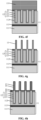
- FIG. 4a to FIG. 4o are schematic diagrams of a semiconductor structure during manufacturing according to an embodiment of the application.
- a schematic diagram may be partially enlarged not according to a general scale, and the schematic diagram is only an example, and should not limit the protection scope of the application herein.
- the substrate 11 is provided.
- the substrate 11 may be a semiconductor substrate, and may include at least one elementary semiconductor material (for example, a silicon (Si) substrate, or a germanium (Ge) substrate), at least one III-V compound semiconductor material, at least one II-VI compound semiconductor material, at least one organic semiconductor material, or other semiconductor materials known in the art.
- the substrate is a silicon substrate.
- the silicon substrate may be doped or undoped.
- the substrate 11 includes a doped area 111 and a first semiconductor layer 112 arranged above the doped area.
- the doped region 111 may be, for example, a Deep N-Well, DNW.
- the first semiconductor layer 112 includes, but is not limited to, silicon germanium.
- the substrate 11 further includes an insulation layer 113.
- the insulation layer is arranged between the doped area 111 and the first semiconductor layer 112. In the actual operation, the substrate may be a wafer.
- S 102 is performed, in which a plurality of capacitors 12 are formed in the substrate 11.
- the operation that the plurality of capacitors 12 are formed includes the following operations.
- a mask layer 20 is deposited above the substrate 11.
- the mask layer 20 and the substrate 11 are patterned to form a plurality of grooves 124.
- a capacitor lower electrode 121, a capacitor dielectric layer 122 and a capacitor upper electrode 123 are sequentially formed in each of the plurality of grooves 124.
- the mask layer 20 is firstly deposited above the substrate 11.
- a material of the mask layer 20 includes, but is not limited to, nitride, for example, may be silicon nitride.
- the mask layer 20 and the substrate 11 are patterned to form the plurality of grooves 124.
- the patterning process may be, for example, a dry etching process, so that the grooves with better morphology and higher size accuracy can be formed.
- the mask layer 20 is configured to protect the top portion of the substrate 11 from being oxidized, nitrided, damaged, or contaminated in subsequent processes.
- the capacitor lower electrode 121, the capacitor dielectric layer 122 and the capacitor upper electrode 123 are sequentially formed in each groove 124.
- Materials of the capacitor upper electrode 123 and the capacitor lower electrode 121 may include a conductive material.
- the conductive material includes, but is not limited to, tungsten (W), copper (Cu), titanium (Ti), tantalum (Ta), titanium nitride (TiN), tantalum nitride (TaN), polycrystalline silicon, doped silicon, metal silicide, metal alloys, or any combination thereof.
- the materials of the capacitor upper electrode 123 and the capacitor lower electrode 121 may be the same.
- a material of the capacitor dielectric layer 122 may be, for example, a High k material.
- S103 is performed, in which a plurality of active pillars 13 are formed above the substrate 11.
- Each of the plurality of active pillars 13 is arranged above a respective one of the plurality of capacitors 12.
- a bottom portion of each of the plurality of active pillar 13 is electrically connected to a top portion of the respective one of the plurality of capacitors 12 therebelow.
- the operation that the plurality of active pillars 13 are formed includes the following operations.
- a second semiconductor layer 131 is deposited above the plurality of capacitors.
- the second semiconductor layer 131 is patterned to form the plurality of active pillars 13.
- Each of the plurality of active pillars 13 is arranged above a respective one of the plurality of capacitors 12.
- the second semiconductor layer 131 is firstly deposited above the capacitors.
- a material of the second semiconductor layer 131 includes Indium Gallium Zinc Oxide, IGZO.
- IGZO Indium Gallium Zinc Oxide
- the transistor since the transistor is formed above the capacitor, a manufacturing process of forming the active pillar by using a conventional semiconductor material (for example, silicon) is complicated.
- the IGZO has the advantages of high mobility, simple manufacturing process, good uniformity, transparency, and low power consumption.
- the IGZO refers to an oxide containing In, Ga and Zn as main components, or may also contain metal elements other than In, Ga, and Zn.
- the IGZO may also contain one or more of tin (Sn), hafnium (Hf), zirconium (Zr), titanium (Ti), scandium (Sc), yttrium (Y), or lanthanides (such as cerium (Ce), neodymium (Nd), gadolinium (Gd)).
- the ratio of In, Ga, and Zn is not limited. Exemplarily, the ratio of In, Ga, and Zn may be 1:1:1, or the ratio of In, Ga, and Zn may be 3:1:2, or the ratio of In, Ga, and Zn may be 2:3:1.
- the IGZO may be formed by PVD magnetron sputtering from targets such as indium, gallium, zinc, oxygen, etc.
- the second semiconductor layer 131 is patterned to form the plurality of active pillars 13.
- Each of the plurality of active pillars 13 is arranged above a respective one of the plurality of capacitors 12.
- the patterning process may be, for example, a dry etching process, so as to form the active pillar with better morphology and higher size accuracy.
- the bottom portion of the active pillar 13 may be electrically connected to the capacitor upper electrode 123.
- the method further includes the following operations.
- a plurality of word lines 14 extending in a first direction are formed, in which the plurality of word lines 14 are arranged above the substrate 11, and each of the plurality of word lines 14 is arranged around a sidewall of a respective one of the plurality of active pillars 13.
- a plurality of bit lines 15 extending in a second direction which intersects with the first direction are formed, in which the plurality of bit lines 15 are arranged above the plurality of active pillars 13, and a bottom portion of each of the plurality of bit lines 15 is electrically connected to top portions of the plurality of active pillars 13.
- the operation that the plurality of word lines 14 are formed includes the following operations.
- a dielectric layer 16 is formed, in which the dielectric layer 16 covers the plurality of active pillars 13.
- a lower filling layer 17 is formed, in which the lower filling layer 17 is partially filled in gaps between any two adjacent active pillars 13 of the plurality of active pillars, and exposes a channel area in each of the plurality of active pillars 13.
- a word line material layer 141 is formed on the lower filling layer 17, and the word line material layer 141 is etched in the first direction to form the plurality of word lines 14 extending in the first direction, in which each of the plurality of word lines is arranged around the channel area in a respective one of the plurality of active pillars.
- An upper filling layer 18 is formed. Planarization is performed to remove the dielectric layer 16 covering the top portions of the plurality of active pillars 13 and to remove the upper filling layer 18 covering the top portions of the plurality of active pillars 13, so as to allow a surface of the upper filling layer 18 to be flush with a surface of each of the plurality of active pillars 13.
- the dielectric layer 16 is firstly formed.
- the dielectric layer 16 covers the active pillars 13.
- a material of the dielectric layer includes, but is not limited to, oxide, for example, may be silicon oxide.
- a process of forming the dielectric layer 16 includes, but is not limited to, an atomic layer deposition process or a thermal oxidation process. In the actual operation, the atomic layer deposition process may be used to form the dielectric layer with a uniform thickness and dense structure on the sidewalls of the active pillars.
- the lower filling layer 17 is formed.
- the lower filling layer 17 is partially filled in gaps between any two adjacent active pillars 13, and exposes the channel area in the active pillar 13.
- the material of the lower filling layer 17 includes, but is not limited to, silicon oxide, silicon nitride, silicon oxynitride or polymeric materials.
- the lower filling layer may be formed through one or more thin film deposition processes, such as an ALD process, a CVD process, etc.
- the word line material layer 141 is formed on the lower filling layer 17, and the word line material layer 141 is etched in the first direction to form the plurality of word lines 14 extending in the first direction.
- the word line is arranged around the channel area in the active pillar.
- the material of the word line 14 may include a conductive material.
- the conductive material includes, but is not limited to, tungsten (W), copper (Cu), titanium (Ti), tantalum (Ta), titanium nitride (TiN), tantalum nitride (TaN), polycrystalline silicon, doped silicon, metal silicide, metal alloys, or any combination thereof.
- the upper filling layer 18 is formed.
- the material of the upper filling layer 18 includes, but is not limited to, silicon oxide, silicon nitride, silicon oxynitride or polymeric materials.
- the upper filling layer may be formed through one or more thin film deposition processes, such as an ALD process, a CVD process, etc. In some embodiments, the materials of the upper filling layer and the lower filling layer may be the same.
- planarization is performed, so as to remove the dielectric layer 16 and the upper filling layer 18 which cover the top portions of the active pillars 13, so that the surface of the upper filling layer 18 is flush with the surface of each active pillar 13.
- the upper filling layer is filled in the gaps between any two adjacent word lines and between any two adjacent active pillars above the word lines.
- the planarization process includes, but is not limited to, chemical mechanical polishing, etching planarization, or a combination thereof.
- the plurality of bit lines 15 extending in a second direction which intersects with the first direction are formed.
- the bit lines 15 are arranged above the active pillars 13, and a bottom portion of each bit line 15 is electrically connected to top portions of the active pillars 13.
- a connection member may further be provided between the bit line 15 and the active pillar 13.
- the bit line 15 is electrically connected to the active pillar 13 through the connection member, so that the contact resistance between the bit line 15 and the active pillar 13 can be reduced.
- the bit line 15 may include a heavily doped area.
- a material of the bit line 15 may include a conductive material.
- the conductive material includes, but is not limited to, tungsten (W), copper (Cu), titanium (Ti), tantalum (Ta), titanium nitride (TiN), tantalum nitride (TaN), polycrystalline silicon, doped silicon, metal silicide, metal alloys, or any combination thereof.
- the method further includes the following operation.
- a contact 19 is formed.
- a bottom portion of the contact 19 is electrically connected to the plurality of capacitors 12. In the actual operation, the contact 19 penetrates through the upper filling layer 18 and the lower filling layer 17. The bottom portion of the contact 19 is electrically connected to the capacitor lower electrode 121.
- a material of the contact may include a conductive material.
- the conductive material includes, but is not limited to, tungsten (W), copper (Cu), titanium (Ti), tantalum (Ta), titanium nitride (TiN), tantalum nitride (TaN), polycrystalline silicon, doped silicon, metal silicide, metal alloys, or any combination thereof.
- the contact may also be formed after the bit lines are formed. In the actual operation, the contact may be arranged on a side of an array area of the active pillar, which is not limited thereto. The contact may also be arranged in the array area of the active pillar, and arranged between the adjacent word lines, and penetrates through the upper filling layer 18 and the lower filling layer 17 between the adjacent word lines.
- the materials of the contact 19 and the bit line 15 may be the same. Specifically, a contact trench is firstly formed. Then, a conductive material is deposited. The conductive material covers the surfaces of the active pillars and is filled in the contact trench. The conductive material filled in the contact trench forms the contact. Finally, the conductive material covering the surfaces of the active pillars is etched, so as to form the plurality of bit lines 15 extending in the second direction which intersects with the first direction. The bit lines 15 are arranged above the active pillars 13, and the bottom portion of the bit line 15 is electrically connected to the top portions of the active pillars 13.
- An embodiment of the application further provides a method for manufacturing a memory.
- the manufacturing method includes the following operations.
- each of the plurality of first chips includes the semiconductor structure described in any one of the above embodiments.
- a wafer is provided, in which the wafer includes a plurality of second chips.
- each of the plurality of first chips is placed on a respective one of the plurality of second chips, in which an active surface of each of the plurality of first chips is arranged face to face with an active surface of the respective one of the plurality of second chips.
- the active surface of each of the plurality of first chips is bumplessly bonded to the active surface of the respective one of the plurality of second chips.
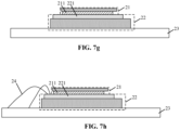
- FIG. 7a to FIG. 7h are schematic diagrams of a memory during manufacturing according to an embodiment of the application.
- a schematic diagram may be partially enlarged not according to a general scale, and the schematic diagram is only an example, and should not limit the protection scope of the application herein.
- the method begins at S601. As shown in FIG. 7a to FIG. 7c , a first chip 21 is provided.
- the first chip 21 includes the semiconductor structure described in any one of the above embodiments.
- the first chip 21 may be a memory array chip, and the memory array chip includes a memory cell array.
- the first chip may further include a circuit assembly.
- the circuit assembly may include, but is not limited to, a transistor, a resistor, a capacitor and an interconnection member, so as to form an IC integrated circuit.
- the operation that the first chip 21 is provided includes the following operation.
- a wafer is provided, in which the wafer includes a plurality of first chips 21.
- the method further includes the following operation.
- a non-active surface of the wafer is thinned.
- an overall thickness of the wafer can be reduced, so that the integration can be further improved.
- the heat transfer path is shortened, so that the heat dissipation efficiency is further improved.
- the method before the non-active surface of the wafer is thinned, the method further includes the following operation.
- a solidified layer is formed above the active surface of the wafer.
- a material of the solidified layer includes, but is not limited to, silicon dioxide, silicon nitride, polymeric materials, or a combination thereof.
- the manufacturing method further includes the following operation.
- the wafer is cut, so as to separate the wafer from the plurality of first chips 21.
- a wafer which includes a plurality of second chips 22.
- the second chip 22 may be a periphery chip.
- the periphery chip includes a peripheral circuit.
- the peripheral circuit may include any appropriate digital, analog and/or mixed-signal circuits that are used to facilitate the operation of the memory cell array.
- the periphery chip may include one or more of a page buffer, a decoder (for example, a row decoder or a column decoder), a sense amplifier, a driver (for example, a word line driver), a charge pump, current or voltage references, or any active or passive component (for example, a transistor, a diode, a resistor or a capacitor) of the circuit.
- the second chip may further include a circuit assembly.
- the circuit assembly may include, but is not limited to, a transistor, a resistor, a capacitor and an interconnection member, so as to form an IC integrated circuit.
- each of the plurality of first chips 21 is placed on a respective one of the plurality of second chips 22, in which an active surface 211 of each of the plurality of first chips is arranged face to face with an active surface 221 of the respective one of the plurality of second chips.
- a projection of each of the plurality of first chips 22 in a vertical direction is covered by a projection of the respective one of the plurality of second chips 21 in the vertical direction. Therefore, a space is reserved for the interconnection between the first chip 21 and the second chip 22 which are bonded to each other and other devices.
- S604 is performed, in which the active surface 211 of each of the plurality of first chips is bumplessly bonded to the active surface 221 of the respective one of the plurality of second chips.
- Bumpless bonding may be, for example, hybrid bonding.
- the manufacturing method further includes the following operations.
- the wafer is cut to separate the wafer from each of the plurality of first chips 21 and the respective one of the plurality of second chips 22 which are bonded to each other.
- a plurality of base plates 23 are provided, in which a projection of each of the plurality of base plates 23 in the vertical direction covers the projection of the respective one of the plurality of second chips 22 in the vertical direction.
- Each of the plurality of first chips 21 and the respective one of the plurality of second chips 22 which are bonded to each other are placed on a respective one of the plurality of base plates 23.
- the respective one of the plurality of base plates 23 is bonded to the respective one of the plurality of second chips 22 through a lead wire 24.
- the wafer is firstly cut to separate the wafer from each of the plurality of first chips 21 and the respective one of the plurality of second chips 22 which are bonded to each other.
- each base plate 23 in the vertical direction covers the projection of the respective second chip 22 in the vertical direction. Therefore, a space can be reserved for the interconnection between the base plate and the second chip 22.
- the base plate may be a Printed Circuit Board, PCB.
- each first chip 21 and the respective second chip 22 which are bonded to each other are placed on a respective one of the base plates 23.
- the respective one of the base plates 23 is bonded to the respective second chip 22 through the lead wire 24.
- one end of the lead wire may be arranged on the active surface of the second chip 22, and the other end of the lead wire may be arranged in a position where the projection of the base plate 23 in the vertical direction does not overlap with the projection of the second chip 22 in the vertical direction.
- the lead wire bonding process has the advantages of simple manufacturing process, low cost, low bonding temperature, high bonding strength and high efficiency.
- the embodiment of the application provides a semiconductor structure.
- the semiconductor structure includes: a substrate; a plurality of capacitors arranged in the substrate; and a plurality of active pillars arranged above the substrate.
- Each of the plurality of active pillars is arranged above a respective one of the plurality of capacitors, and a bottom portion of each of the plurality of active pillars is electrically connected to a top portion of the respective one of the plurality of capacitors therebelow.
- each active pillar is arranged above the respective capacitor. That is to say, a transistor is arranged above the capacitor.
- the bit line electrically connected to the active pillar may be directly formed on the top portion of the active pillar, without the need for additional manufacture a contact and an interconnection line to lead out a bit line signal, so that the process is simplified. Further, since the bit line is directly formed on the top portion of the active pillar, that is, the bit line is formed on an active surface of a memory array chip, so that a Chip On Wafer, COW, process may be conveniently used later. With less interconnection lines and contacts, the memory array chip and the peripheral circuit wafer can be directly and bumplessly connected to each other in the vertical direction in a face-to-face manner. In this way, the space utilization is effectively improved, and the signal interconnection paths are reduced, thereby reducing the thermal resistance, and improving the signal transmission speed.
- the semiconductor structure, the method for manufacturing the semiconductor structure, the memory and the method for manufacturing the memory provided in the embodiments of the application can be applied to any integrated circuit including these structures.
- the technical features in the technical solutions described in the embodiments may be arbitrarily combined with each other without conflict.
- Those skilled in the art can change the sequence of the operations in the above formation method without departing from the protection scope of the application. Some operations in the embodiments of the application may be simultaneously performed or may be sequentially perform without conflict.
- each active pillar is arranged above the respective capacitor. That is to say, a transistor is arranged above the capacitor.
- the bit line electrically connected to the active pillar may be directly formed on the top portion of the active pillar, without the need for additional manufacture a contact and an interconnection line to lead out a bit line signal, so that the process is simplified.
- the bit line is directly formed on the top portion of the active pillar, that is, the bit line is formed on an active surface of a memory array chip, so that a Chip On Wafer, COW, process may be conveniently used later.
- the memory array chip and the peripheral circuit wafer can be directly and bumplessly connected to each other in the vertical direction in a face-to-face manner. In this way, the space utilization is effectively improved, and the signal interconnection paths are reduced, thereby reducing the thermal resistance, and improving the signal transmission speed.
Landscapes
- Engineering & Computer Science (AREA)
- Manufacturing & Machinery (AREA)
- Semiconductor Memories (AREA)
Abstract
Description
- This application is based upon and claims priority to
Chinese Patent Application No. 202210730103.8, filed on June 24, 2022 - The application relates to the technical field of semiconductors, and in particular to a semiconductor structure, a method for manufacturing a semiconductor structure, a memory, and a method for manufacturing a memory.
- A memory (for example, a Dynamic Random Access Memory, DRAM) usually includes a memory array circuit and a peripheral circuit. The memory array circuit generally consists of a plurality of memory cells arranged in an array. The memory cell generally consists of a transistor and a capacitor. Currently, a process for manufacturing the DRAM is complicated, and a signal interconnection path is long, which limits the storage capacity and integration of the DRAM.
- Therefore, how to optimize the structure and process of the DRAM to achieve higher integration has become an urgent problem to be solved.
- An embodiment of the application provides a semiconductor structure, which includes: a substrate; a plurality of capacitors arranged in the substrate; and a plurality of active pillars arranged above the substrate. Each of the plurality of active pillars is arranged above a respective one of the plurality of capacitors, and a bottom portion of each of the plurality of active pillars is electrically connected to a top portion of the respective one of the plurality of capacitors therebelow.
- In some embodiments, the semiconductor structure further includes: a plurality of word lines extending in a first direction, in which the plurality of word lines are arranged above the substrate, and each of the plurality of word lines is arranged around a sidewall of a respective one of the plurality of active pillars; and a plurality of bit lines extending in a second direction which intersects with the first direction, in which the plurality of bit lines are arranged above the plurality of active pillars, and a bottom portion of each of the plurality of bit lines are electrically connected to top portions of the plurality of active pillars.
- In some embodiments, the semiconductor structure further includes: a dielectric layer arranged above the substrate and covering the sidewalls of the plurality of active pillars; a lower filling layer filled in gaps between any two adjacent active pillars of the plurality of active pillars below the plurality of word lines; and an upper filling layer filled in gaps between any two adjacent word lines of the plurality of word lines and gaps between any two adjacent active pillars of the plurality of active pillars above the plurality of word lines.
- In some embodiments, the semiconductor structure further includes a contact. The contact penetrates through the upper filling layer and the lower filling layer. A bottom portion of the contact is electrically connected to the plurality of capacitors.
- In some embodiments, a material of each of the plurality of active pillars comprises indium gallium zinc oxide.
- An embodiment of the application provides a memory, which includes: a first chip including the semiconductor structure described in any one of the above embodiments; and a second chip including a peripheral circuit. An active surface of the first chip is bumplessly bonded to an active surface of the second chip.
- In some embodiments, the second chip is arranged below the first chip. A projection of the second chip in a vertical direction covers a projection of the first chip in the vertical direction.
- In some embodiments, the memory further includes a base plate arranged below the second chip. A projection of the base plate in the vertical direction covers the projection of the second chip in the vertical direction. The base plate is bonded to the second chip through a lead wire.
- An embodiment of the application further provides a method for manufacturing a semiconductor structure, which includes the following operations. A substrate is provided. A plurality of capacitors are formed in the substrate. A plurality of active pillars are formed above the substrate, in which each of the plurality of active pillars is arranged above a respective one of the plurality of capacitors, and a bottom portion of each of the plurality of active pillars is electrically connected to a top portion of the respective one of the plurality of capacitors therebelow.
- In some embodiments, after the plurality of active pillars are formed, the method further includes the following operations. A plurality of word lines extending in a first direction are formed, in which the plurality of word lines are arranged above the substrate, and each of the plurality of word lines is arranged around a sidewall of a respective one of the plurality of active pillars. A plurality of bit lines extending in a second direction which intersects with the first direction are formed, in which the plurality of bit lines are arranged above the plurality of active pillars, and a bottom portion of each of the plurality of bit lines is electrically connected to top portions of the plurality of active pillars.
- In some embodiments, before the plurality of bit lines are formed, the method further includes the following operation. A contact is formed, in which a bottom portion of the contact is electrically connected to the plurality of capacitors.
- In some embodiments, the operation that the plurality of capacitors are formed includes the following operations. A mask layer is deposited above the substrate. The mask layer and the substrate are patterned to form a plurality of grooves. A capacitor lower electrode, a capacitor dielectric layer and a capacitor upper electrode are sequentially formed in each of the plurality of grooves.
- In some embodiments, the operation that the plurality of active pillars are formed includes the following operations. A semiconductor layer is formed above the plurality of capacitors. The semiconductor layer is patterned to form the plurality of active pillars, in which each of the plurality of active pillars is arranged above the respective one of the plurality of capacitors.
- In some embodiments, the operation that the plurality of word lines are formed includes the following operations. A dielectric layer is formed, in which the dielectric layer covers the plurality of active pillars. A lower filling layer is formed, in which the lower filling layer is partially filled in gaps between any two adjacent active pillars of the plurality of active pillars, and exposes a channel area in each of the plurality of active pillars. A word line material layer is formed on the lower filling layer, and the word line material layer is etched in the first direction to form the plurality of word lines extending in the first direction, in which each of the plurality of word lines is arranged around the channel area in a respective one of the plurality of active pillars. An upper filling layer is formed. Planarization is performed to remove the dielectric layer covering the top portions of the plurality of active pillars and to remove the upper filling layer covering the top portions of the plurality of active pillars, so as to allow a surface of the upper filling layer to be flush with a surface of each of the plurality of active pillars.
- An embodiment of the application further provides a method for manufacturing a memory, which includes the following operations. A plurality of first chips are provided, in which each of the plurality of first chips includes the semiconductor structure described in any one of the above embodiments. A wafer is provided, in which the wafer includes a plurality of second chips. Each of the plurality of first chips is placed on a respective one of the plurality of second chips, in which an active surface of each of the plurality of first chips is arranged face to face with an active surface of the respective one of the plurality of second chips. The active surface of each of the plurality of first chips is bumplessly bonded to the active surface of the respective one of the plurality of second chips.
- In some embodiments, a projection of each of the plurality of first chips in a vertical direction is covered by a projection of the respective one of the plurality of second chips in the vertical direction.
- In some embodiments, the manufacturing method further includes the following operations. The wafer is cut to separate the wafer from each of the plurality of first chips and the respective one of the plurality of second chips which are bonded to each other. A plurality of base plates are provided, in which a projection of each of the plurality of base plates in the vertical direction covers the projection of the respective one of the plurality of second chips in the vertical direction. Each of the plurality of first chips and the respective one of the plurality of second chips which are bonded to each other is placed on a respective one of the plurality of base plates. The respective one of the plurality of base plates is bonded to the respective one of the plurality of second chips through a lead wire.
- The embodiment of the application provides a semiconductor structure. The semiconductor structure includes: a substrate; a plurality of capacitors arranged in the substrate; and a plurality of active pillars arranged above the substrate. Each of the plurality of active pillars is arranged above a respective one of the plurality of capacitors, and a bottom portion of each of the plurality of active pillars is electrically connected to a top portion of the respective one of the plurality of capacitors therebelow. In the embodiments of the application, each active pillar is arranged above the respective capacitor. That is to say, a transistor is arranged above the capacitor. In this way, the bit line electrically connected to the active pillar may be directly formed on the top portion of the active pillar, without the need for additional manufacture a contact and an interconnection line to lead out a bit line signal, so that the process is simplified. Further, since the bit line is directly formed on the top portion of the active pillar, that is, the bit line is formed on an active surface of a memory array chip, so that a Chip On Wafer, COW, process may be conveniently used later. With less interconnection lines and contacts, the memory array chip and the peripheral circuit wafer can be directly and bumplessly connected to each other in the vertical direction in a face-to-face manner. In this way, the space utilization is effectively improved, and the signal interconnection paths are reduced, thereby reducing the thermal resistance, and improving the signal transmission speed.
- In order to describe the technical solutions in the embodiments of the application or conventional technologies more clearly, the accompanying drawings required to be used in the embodiments of the application will be simply introduced below. Apparently, the accompanying drawings in the following description show merely some embodiments of the application, and persons of ordinary skill in the art may still derive other drawings from these accompanying drawings without creative effort.
-
FIG. 1 is a schematic cross-sectional view of a semiconductor structure according to an embodiment of the application; -
FIG. 2a is a schematic vertical cross-sectional view of a memory according to an embodiment of the application; -
FIG. 2b is a schematic three-dimensional diagram of a memory according to an embodiment of the application; -
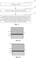
FIG. 3 is a flowchart of a method for manufacturing a semiconductor structure according to an embodiment of the application; -
FIG. 4a to FIG. 4o are schematic diagrams of a semiconductor structure during manufacturing according to an embodiment of the application; -
FIG. 5a is a cross-sectional view taken along a dotted line AA' inFIG. 4m ; -
FIG. 5b is a cross-sectional view taken along a dotted line BB' inFIG. 4m ; -
FIG. 6 is a flowchart of a method for manufacturing a memory according to an embodiment of the application; and -
FIG. 7a to FIG. 7h are schematic diagrams of a memory during manufacturing according to an embodiment of the application. - Reference numerals:
11-Substrate; 111-Doped area; 112-First semiconductor layer; 113-Insulation layer; 12-Capacitor; 121-Capacitor lower electrode; 122-Capacitor dielectric layer; 123-Capacitor upper electrode; 124-Groove; 13-Active pillar; 131-Second semiconductor layer; 14-Word line; 15-Bit line; 16-Dielectric layer; 17-Lower filling layer; 18-Upper filling layer; 19-Contact; 20-Mask layer; 21-First chip; 211-Active surface of first chip; 22-Second chip; 221-Active surface of second chip; 23-Base plate; 24-Lead wire. - Exemplary embodiments disclosed in the application will be described in more detail below with reference to the accompanying drawings. Although the exemplary embodiments of the present application are shown in the accompanying drawings, it should be understood that the present application can be implemented in various forms and cannot be limited by the embodiments illustrated herein. On the contrary, these embodiments are provided to more thoroughly understand the present application and to completely convey the scope of the present application to those skilled in the art.
- In the following descriptions, numerous specific details are set forth in order to provide a more thorough understanding of the present application. However, it will be apparent to those skilled in the art that the present application can be implemented without one or more of these details. In other examples, in order to avoid confusion with the present application, some technical features known in the art are not described. That is, all the features of the actual embodiments are not described here, and the well-known functions and structures are not described in detail.
- In the accompanying drawings, the sizes and relative size of layers, regions, and elements may be exaggerated for clarity. The same reference numerals denote the same elements throughout the application.
- It should be understood that, when an element or layer is described as being "on", "adjacent to", "connected to" or "coupled to" another element or layer, it can be directly on, adjacent to, connected to, or coupled to the other element or layer, or there can be an intermediate element or layer. In contrast, when an element is described as being "directly on", "directly adjacent to", "directly connected to" or "directly coupled to" another element or layer, there is no intermediate element or layer. It should be understood that although the terms "first", "second", "third" and so on may be used to describe various elements, components, regions, layers, and/or portions, these elements, components, regions, layers, and/or portions should not be limited by these terms. These terms are used merely to distinguish an element, component, region, layer, or portion from another element, component, region, layer, or portion. Therefore, a first element, component, region, layer, or portion discussed below may be described as a second element, component, region, layer, or portion without departing from the teachings of the present application. When the second element, component, region, layer or portion is discussed, it does not mean that the first element, component, region, layer or portion is necessarily present in the present application.
- Terms used herein are for the purpose of describing specific embodiments only and are not intended to be limiting of the present application. As used herein, "a/an", "one", and "the" in singular forms are also intended to include a plural form unless the context clearly indicates other forms. It should also be understood that the terms "consist" and/or "include" when used in the description, determine presence of the features, integers, steps, operations, elements, and/or components, but do not exclude the presence or addition of one or more other features, integers, steps, operations, elements, components, and/or groups. As used herein, the term "and/or" includes any and all combinations of the related listed items.
- Since the cell size of a semiconductor device (for example, Dynamic Random Access Memory, DRAM) is continuously reduced, the DRAM with a planar transistor layout using a conventional 6F2 architecture design can no longer meet requirements due to the short channel effect. At present, the DRAM with a vertical transistor layout using a 4F2 architecture design has been introduced into the industry. In the DRAM with the vertical transistor layout, a bit line of a vertical transistor is generally arranged at the bottom portion of an active pillar, and a capacitor is arranged above the active pillar. In this structure, bit line signals and word line signals needs to be interconnected with other devices through a plurality of metal lines and contacts, so that the space utilization is low, the signal interconnection paths are complicated, and the packaging performance is poor.
- Based on this, an embodiment of the application provides a semiconductor structure.
FIG. 1 is a schematic cross-sectional view of a semiconductor structure according to an embodiment of the application. - With reference to
FIG. 1 , the semiconductor structure includes: asubstrate 11; a plurality ofcapacitors 12 arranged in thesubstrate 11; and a plurality ofactive pillars 13 arranged above thesubstrate 11. Each of the plurality ofactive pillars 13 is arranged above a respective one of the plurality ofcapacitors 12, and a bottom portion of each of the plurality ofactive pillars 13 is electrically connected to a top portion of the respective one of the plurality ofcapacitors 12 therebelow. - In the embodiments of the application, each active pillar is arranged above the respective capacitor. That is to say, a transistor is arranged above the capacitor. In this way, the bit line electrically connected to the active pillar may be directly formed on the top portion of the active pillar, without the need for additional manufacture a contact and an interconnection line to lead out a bit line signal, so that the process is simplified. Further, since the bit line is directly formed on the top portion of the active pillar, that is, the bit line is formed on an active surface of a memory array chip, so that a Chip On Wafer, COW, process may be conveniently used later. With less interconnection lines and contacts, the memory array chip and the peripheral circuit wafer can be directly and bumplessly connected to each other in a vertical direction in a face-to-face manner. In this way, the space utilization is effectively improved, and the signal interconnection paths are reduced, thereby reducing the thermal resistance, and improving the signal transmission speed.
- The
substrate 11 may be a semiconductor substrate, and may include at least one elementary semiconductor material (for example, a silicon (Si) substrate, a germanium (Ge) substrate), at least one III-V compound semiconductor material, at least one II-VI compound semiconductor material, at least one organic semiconductor material, or other semiconductor materials known in the art. In a specific embodiment, the substrate is a silicon substrate. The silicon substrate may be doped or undoped. In some other embodiments, thesubstrate 11 includes a dopedarea 111 and afirst semiconductor layer 112 arranged above the doped area. Thecapacitors 12 are arranged in thefirst semiconductor layer 112. The dopedarea 111 may be, for example, a Deep N-Well, DNW. Thefirst semiconductor layer 112 includes, but is not limited to, silicon germanium. In some more specific embodiments, thesubstrate 11 further includes aninsulation layer 113. The insulation layer is arranged between the dopedarea 111 and thefirst semiconductor layer 112. In the actual operation, the substrate may be a wafer. - In some embodiments, with reference to
FIG. 1 , the semiconductor structure further includes a plurality ofword lines 14 extending in a first direction and a plurality ofbit lines 15 extending in a second direction which intersects with the first direction. The plurality ofword lines 14 are arranged above thesubstrate 11, and each of the plurality of word lines 14 is arranged around a sidewall of a respective one of the plurality ofactive pillars 13. The plurality ofbit lines 15 are arranged above the plurality ofactive pillars 13, and a bottom portion of each of the plurality ofbit lines 15 is electrically connected to top portions of the plurality ofactive pillars 13. In this way, the bit lines are directly formed on the top portions of the active pillars, so that the number of the interconnection lines and the contacts is greatly reduced, thereby improving the space utilization, and shortening the signal transmission distance. Herein, a material of theword line 14 may include a conductive material. The conductive material includes, but is not limited to, tungsten (W), copper (Cu), titanium (Ti), tantalum (Ta), titanium nitride (TiN), tantalum nitride (TaN), polycrystalline silicon, doped silicon, metal silicide, metal alloys, or any combination thereof. In other embodiments, a connection member may further be provided between thebit line 15 and theactive pillar 13. Thebit line 15 is electrically connected to theactive pillar 13 through the connection member, thereby reducing the contact resistance between thebit line 15 and theactive pillar 13. In the actual operation, thebit line 15 may include a heavily doped area. A material of thebit line 15 may include a conductive material. The conductive material includes, but is not limited to, tungsten (W), copper (Cu), titanium (Ti), tantalum (Ta), titanium nitride (TiN), tantalum nitride (TaN), polycrystalline silicon, doped silicon, metal silicide, metal alloys, or any combination thereof. - In some embodiments, the area of the
active pillar 13 which is surrounded by theword line 14 includes a channel doped area. Each of an upper portion and a lower portion of theactive pillar 13 which is not surrounded by theword line 14 includes a source/drain doped area. Each of the upper portion and the lower portion of the active pillar is configured as a source or a drain of a vertical transistor. A doping type of the channel doped area is opposite to a doping type of the source/drain doped area. - In some embodiments, with reference to
FIG. 1 , the semiconductor structure further includes: adielectric layer 16 arranged above thesubstrate 11 and covering the sidewalls of the plurality ofactive pillars 13; alower filling layer 17 filled in gaps between any two adjacentactive pillars 13 of the plurality of active pillars below the plurality ofword lines 14; and anupper filling layer 18 filled in gaps between any two adjacent word lines 14 of the plurality of word lines and gaps between any two adjacentactive pillars 13 of the plurality of active pillars above the plurality of word lines 14. A material of the dielectric layer includes, but is not limited to, oxide, for example, may be silicon oxide. A process of forming thedielectric layer 16 includes, but is not limited to, an atomic layer deposition process or a thermal oxidation process. In the actual operation, the atomic layer deposition process may be used to form the dielectric layer with a uniform thickness and a dense structure on the sidewalls of the active pillars. Materials of thelower filling layer 17 and theupper filling layer 18 include, but are not limited to, silicon oxide, silicon nitride, silicon oxynitride or polymeric materials. In some embodiments, the materials of the upper filling layer and the lower filling layer may be the same. The upper filling layer and the lower filling layer may be formed through one or more thin film deposition processes, such as an Atomic Layer Deposition, ALD, process, a Chemical Vapor Deposition, CVD, process, etc. - In some embodiments, with reference to
FIG. 1 , the semiconductor structure further includes amask layer 20. Themask layer 20 at least covers an upper surface of thesubstrate 11, and is configured to protect the top portion of thesubstrate 11 from being oxidized, nitrided, damaged or contaminated in subsequent processes. A material of themask layer 20 includes, but is not limited to, nitride, for example, may be silicon nitride. Herein, the materials of the mask layer, the upper filling layer and the lower filling layer may be the same. - In some embodiments, with reference to
FIG. 1 , the semiconductor structure further includes acontact 19. Thecontact 19 penetrates through theupper filling layer 18 and thelower filling layer 17. A bottom portion of thecontact 19 is electrically connected to the plurality ofcapacitors 12. A material of the contact may include a conductive material. The conductive material includes, but is not limited to, tungsten (W), copper (Cu), titanium (Ti), tantalum (Ta), titanium nitride (TiN), tantalum nitride (TaN), polycrystalline silicon, doped silicon, metal silicide, metal alloys, or any combination thereof. In some embodiments, the materials of thecontact 19 and thebit line 15 may be the same. In the actual operation, the contact may be arranged on a side of an array area of the active pillar, which is not limited thereto. The contact may also be arranged in the array area of the active pillar, and arranged between two adjacent word lines, and penetrate through theupper filling layer 18 and thelower filling layer 17 between the adjacent word lines. - In some embodiments, with reference to
FIG. 1 , thecapacitor 12 includes a capacitorupper electrode 123, acapacitor dielectric layer 122 and a capacitorlower electrode 121. Thecapacitor dielectric layer 122 is arranged between the capacitorupper electrode 123 and the capacitorlower electrode 121. A bottom portion of thecontact 19 is electrically connected to the capacitorlower electrode 121. The bottom portion of theactive pillar 13 is electrically connected to the capacitorupper electrode 123. Materials of the capacitorupper electrode 123 and the capacitorlower electrode 121 may include a conductive material. The conductive material includes, but is not limited to, tungsten (W), copper (Cu), titanium (Ti), tantalum (Ta), titanium nitride (TiN), tantalum nitride (TaN), polycrystalline silicon, doped silicon, metal silicide, metal alloys, or any combination thereof. In some embodiments, the materials of the capacitorupper electrode 123 and the capacitorlower electrode 121 may be the same. A material of thecapacitor dielectric layer 122 may be, for example, a High k material. - In some embodiments, a material of the
active pillar 13 includes Indium Gallium Zinc Oxide, IGZO. In the embodiments of the application, since the transistor is formed above the capacitor, a manufacturing process of forming the active pillar by using a conventional semiconductor material (for example, silicon) is complicated. The IGZO has the advantages of high mobility, simple manufacturing process, good uniformity, transparency, and low power consumption. Herein, the IGZO refers to an oxide containing In, Ga and Zn as main components, and may also contain metal elements other than In, Ga, and Zn. For example, the IGZO may also contain one or more of tin (Sn), hafnium (Hf), zirconium (Zr), titanium (Ti), scandium (Sc), yttrium (Y), or lanthanides (such as cerium (Ce), neodymium (Nd), gadolinium (Gd)). It should be understood that, the ratio of In, Ga, and Zn is not limited. Exemplarily, the ratio of In, Ga, and Zn may be 1:1:1, or the ratio of In, Ga, and Zn may be 3:1:2, or the ratio of In, Ga, and Zn may be 2:3:1. In the actual operation, the IGZO may be formed by PVD magnetron sputtering from targets such as indium, gallium, zinc, oxygen, etc. Herein, the upper portion and the lower portion of theactive pillar 13 which are not surrounded by theword line 14 may form the source/drain doped area through an in-situ doping process. Exemplarily, the source/drain doped area may be formed by correspondingly injecting an N-type element (for example, arsenic (As) element or phosphorus (P) element), so as to finally form an N-type transistor. It should be understood that, the material of the active pillar may also be other III-V semiconductor materials or oxide semiconductor materials. - An embodiment of the application provides a memory.
FIG. 2a is a schematic vertical cross-sectional view of a memory according to an embodiment of the application.FIG. 2b is a schematic three-dimensional diagram of a memory according to an embodiment of the application. - With reference to
FIG. 2a and FIG. 2b , the memory includes: afirst chip 21 including the semiconductor structure described in any one of the above embodiments; and asecond chip 22 including a peripheral circuit. Anactive surface 211 of the first chip is bumplessly bonded to anactive surface 221 of the second chip. Herein, thefirst chip 21 may be a memory array chip. Thesecond chip 22 may be a periphery chip. Herein, the memory array chip includes a memory cell array. The periphery chip includes a peripheral circuit. The peripheral circuit may include any appropriate digital, analog and/or mixed-signal circuits that are used to facilitate the operation of the memory cell array. For example, the periphery circuit may include one or more of a page buffer, a decoder (for example, a row decoder or a column decoder), a sense amplifier, a driver (for example, a word line driver), a charge pump, current or voltage references, or any active or passive component (for example, a transistor, a diode, a resistor or a capacitor) of the circuit. The first chip and the second chip may further include circuit assemblies. The circuit assemblies may include, but are not limited to, transistors, resistors, capacitors and interconnection members, so as to form an IC integrated circuit. Bumpless bonding may be, for example, hybrid bonding. Since the transistor of the memory array chip is arranged above the capacitor, the bit line may be directly formed on the active surface. In this way, with less interconnection lines and contacts, the memory array chip and the periphery chip can be directly and bumplessly connected to each other in the vertical direction in a face-to-face manner. In this way, the space utilization is effectively improved, and the signal interconnection paths are reduced, thereby reducing the thermal resistance, and improving the signal transmission speed. - In some embodiments, with reference to
FIG. 2a and FIG. 2b , thesecond chip 22 is arranged below thefirst chip 21. A projection of thesecond chip 22 in a vertical direction covers a projection of thefirst chip 21 in the vertical direction, so as to reserve the space for the interconnection between thefirst chip 21 and thesecond chip 22 which are bonded to each other and other devices. An end of the interconnection member may be arranged in a position where the projection of thesecond chip 22 in the vertical direction does not overlap with the projection of thefirst chip 21 in the vertical direction. - In some embodiments, with reference to
FIG. 2a and FIG. 2b , the semiconductor structure further includes abase plate 23. Thebase plate 23 is arranged below thesecond chip 22. A projection of thebase plate 23 in the vertical direction covers the projection of thesecond chip 22 in the vertical direction. Thebase plate 23 is bonded to thesecond chip 22 through alead wire 24. The lead wire includes, but is not limited to, a gold wire, a copper wire, an aluminum wire, or a combination thereof. The base plate may be a Printed Circuit Board, PCB. Herein, one end of the lead wire may be arranged on the active surface of thesecond chip 22, and the other end of the lead wire may be arranged in a position where the projection of thebase plate 23 in the vertical direction does not overlap with the projection of thesecond chip 22 in the vertical direction. In this way, electric interconnection and information communication between thefirst chip 21, thesecond chip 22 and the base plate can be achieved by bonding through the lead wire. The lead wire bonding process has the advantages of simple manufacturing process, low cost, low bonding temperature, high bonding strength and high efficiency. - An embodiment of the application further provides a method for manufacturing a semiconductor structure. With reference to
FIG. 3 , the manufacturing method includes the following operations. - In S301, a substrate is provided.
- In S302, a plurality of capacitors are formed in the substrate.
- In S303, a plurality of active pillars are formed above the substrate, in which each of the plurality of active pillars is arranged above a respective one of the plurality of capacitors, and a bottom portion of each of the plurality of active pillars is electrically connected to a top portion of the respective one of the plurality of capacitors therebelow.
- Specific implementations of the application are described in detail below with reference to
FIG. 4a to FIG. 4o. FIG. 4a to FIG. 4o are schematic diagrams of a semiconductor structure during manufacturing according to an embodiment of the application. For convenience of description, a schematic diagram may be partially enlarged not according to a general scale, and the schematic diagram is only an example, and should not limit the protection scope of the application herein. - The method begins at S301. As shown in
FIG. 4a , thesubstrate 11 is provided. Thesubstrate 11 may be a semiconductor substrate, and may include at least one elementary semiconductor material (for example, a silicon (Si) substrate, or a germanium (Ge) substrate), at least one III-V compound semiconductor material, at least one II-VI compound semiconductor material, at least one organic semiconductor material, or other semiconductor materials known in the art. In a specific embodiment, the substrate is a silicon substrate. The silicon substrate may be doped or undoped. In some other embodiments, thesubstrate 11 includes a dopedarea 111 and afirst semiconductor layer 112 arranged above the doped area. The dopedregion 111 may be, for example, a Deep N-Well, DNW. Thefirst semiconductor layer 112 includes, but is not limited to, silicon germanium. In some more specific embodiments, thesubstrate 11 further includes aninsulation layer 113. The insulation layer is arranged between the dopedarea 111 and thefirst semiconductor layer 112. In the actual operation, the substrate may be a wafer. - Next, as shown in
FIG. 4b to FIG. 4e , S 102 is performed, in which a plurality ofcapacitors 12 are formed in thesubstrate 11. - In some embodiments, with reference to
FIG. 4b to FIG. 4e , the operation that the plurality ofcapacitors 12 are formed includes the following operations. Amask layer 20 is deposited above thesubstrate 11. Themask layer 20 and thesubstrate 11 are patterned to form a plurality ofgrooves 124. A capacitorlower electrode 121, acapacitor dielectric layer 122 and a capacitorupper electrode 123 are sequentially formed in each of the plurality ofgrooves 124. - Specifically, as shown in
FIG. 4b , themask layer 20 is firstly deposited above thesubstrate 11. A material of themask layer 20 includes, but is not limited to, nitride, for example, may be silicon nitride. - Next, with reference to
FIG. 4c , themask layer 20 and thesubstrate 11 are patterned to form the plurality ofgrooves 124. The patterning process may be, for example, a dry etching process, so that the grooves with better morphology and higher size accuracy can be formed. Themask layer 20 is configured to protect the top portion of thesubstrate 11 from being oxidized, nitrided, damaged, or contaminated in subsequent processes. - Then, as shown in
FIG. 4b andFIG. 4e , the capacitorlower electrode 121, thecapacitor dielectric layer 122 and the capacitorupper electrode 123 are sequentially formed in eachgroove 124. Materials of the capacitorupper electrode 123 and the capacitorlower electrode 121 may include a conductive material. The conductive material includes, but is not limited to, tungsten (W), copper (Cu), titanium (Ti), tantalum (Ta), titanium nitride (TiN), tantalum nitride (TaN), polycrystalline silicon, doped silicon, metal silicide, metal alloys, or any combination thereof. In some embodiments, the materials of the capacitorupper electrode 123 and the capacitorlower electrode 121 may be the same. A material of thecapacitor dielectric layer 122 may be, for example, a High k material. - Finally, with reference to
FIG. 4f and FIG. 4g , S103 is performed, in which a plurality ofactive pillars 13 are formed above thesubstrate 11. Each of the plurality ofactive pillars 13 is arranged above a respective one of the plurality ofcapacitors 12. A bottom portion of each of the plurality ofactive pillar 13 is electrically connected to a top portion of the respective one of the plurality ofcapacitors 12 therebelow. - In some embodiments, the operation that the plurality of
active pillars 13 are formed includes the following operations. Asecond semiconductor layer 131 is deposited above the plurality of capacitors. Thesecond semiconductor layer 131 is patterned to form the plurality ofactive pillars 13. Each of the plurality ofactive pillars 13 is arranged above a respective one of the plurality ofcapacitors 12. - Specifically, with reference to
FIG. 4f , thesecond semiconductor layer 131 is firstly deposited above the capacitors. In the actual operation, a material of thesecond semiconductor layer 131 includes Indium Gallium Zinc Oxide, IGZO. In the embodiments of the application, since the transistor is formed above the capacitor, a manufacturing process of forming the active pillar by using a conventional semiconductor material (for example, silicon) is complicated. The IGZO has the advantages of high mobility, simple manufacturing process, good uniformity, transparency, and low power consumption. Herein, the IGZO refers to an oxide containing In, Ga and Zn as main components, or may also contain metal elements other than In, Ga, and Zn. For example, the IGZO may also contain one or more of tin (Sn), hafnium (Hf), zirconium (Zr), titanium (Ti), scandium (Sc), yttrium (Y), or lanthanides (such as cerium (Ce), neodymium (Nd), gadolinium (Gd)). It should be understood that, the ratio of In, Ga, and Zn is not limited. Exemplarily, the ratio of In, Ga, and Zn may be 1:1:1, or the ratio of In, Ga, and Zn may be 3:1:2, or the ratio of In, Ga, and Zn may be 2:3:1. In the actual operation, the IGZO may be formed by PVD magnetron sputtering from targets such as indium, gallium, zinc, oxygen, etc. - Next, as shown in
FIG. 4g , thesecond semiconductor layer 131 is patterned to form the plurality ofactive pillars 13. Each of the plurality ofactive pillars 13 is arranged above a respective one of the plurality ofcapacitors 12. The patterning process may be, for example, a dry etching process, so as to form the active pillar with better morphology and higher size accuracy. In the actual operation, the bottom portion of theactive pillar 13 may be electrically connected to the capacitorupper electrode 123. - In some embodiments, with reference to
FIG. 4h to FIG. 4n , after the plurality ofactive pillars 13 are formed, the method further includes the following operations. A plurality ofword lines 14 extending in a first direction are formed, in which the plurality ofword lines 14 are arranged above thesubstrate 11, and each of the plurality of word lines 14 is arranged around a sidewall of a respective one of the plurality ofactive pillars 13. A plurality ofbit lines 15 extending in a second direction which intersects with the first direction are formed, in which the plurality ofbit lines 15 are arranged above the plurality ofactive pillars 13, and a bottom portion of each of the plurality ofbit lines 15 is electrically connected to top portions of the plurality ofactive pillars 13. - In some embodiments, with reference to
FIG. 4h to FIG. 4m , the operation that the plurality ofword lines 14 are formed includes the following operations. Adielectric layer 16 is formed, in which thedielectric layer 16 covers the plurality ofactive pillars 13. Alower filling layer 17 is formed, in which thelower filling layer 17 is partially filled in gaps between any two adjacentactive pillars 13 of the plurality of active pillars, and exposes a channel area in each of the plurality ofactive pillars 13. A wordline material layer 141 is formed on thelower filling layer 17, and the wordline material layer 141 is etched in the first direction to form the plurality ofword lines 14 extending in the first direction, in which each of the plurality of word lines is arranged around the channel area in a respective one of the plurality of active pillars. Anupper filling layer 18 is formed. Planarization is performed to remove thedielectric layer 16 covering the top portions of the plurality ofactive pillars 13 and to remove theupper filling layer 18 covering the top portions of the plurality ofactive pillars 13, so as to allow a surface of theupper filling layer 18 to be flush with a surface of each of the plurality ofactive pillars 13. - Specifically, with reference to
FIG. 4h , thedielectric layer 16 is firstly formed. Thedielectric layer 16 covers theactive pillars 13. A material of the dielectric layer includes, but is not limited to, oxide, for example, may be silicon oxide. A process of forming thedielectric layer 16 includes, but is not limited to, an atomic layer deposition process or a thermal oxidation process. In the actual operation, the atomic layer deposition process may be used to form the dielectric layer with a uniform thickness and dense structure on the sidewalls of the active pillars. - Next, as shown in
FIG. 4i , thelower filling layer 17 is formed. Thelower filling layer 17 is partially filled in gaps between any two adjacentactive pillars 13, and exposes the channel area in theactive pillar 13. The material of thelower filling layer 17 includes, but is not limited to, silicon oxide, silicon nitride, silicon oxynitride or polymeric materials. The lower filling layer may be formed through one or more thin film deposition processes, such as an ALD process, a CVD process, etc. - Next, as shown in
FIG. 4j and FIG. 4k , the wordline material layer 141 is formed on thelower filling layer 17, and the wordline material layer 141 is etched in the first direction to form the plurality ofword lines 14 extending in the first direction. The word line is arranged around the channel area in the active pillar. The material of theword line 14 may include a conductive material. The conductive material includes, but is not limited to, tungsten (W), copper (Cu), titanium (Ti), tantalum (Ta), titanium nitride (TiN), tantalum nitride (TaN), polycrystalline silicon, doped silicon, metal silicide, metal alloys, or any combination thereof. - Then, as shown in
FIG. 4l , theupper filling layer 18 is formed. The material of theupper filling layer 18 includes, but is not limited to, silicon oxide, silicon nitride, silicon oxynitride or polymeric materials. The upper filling layer may be formed through one or more thin film deposition processes, such as an ALD process, a CVD process, etc. In some embodiments, the materials of the upper filling layer and the lower filling layer may be the same. - Next, as shown in
FIG. 4m , planarization is performed, so as to remove thedielectric layer 16 and theupper filling layer 18 which cover the top portions of theactive pillars 13, so that the surface of theupper filling layer 18 is flush with the surface of eachactive pillar 13. As shown inFIG. 5a and FIG. 5b , the upper filling layer is filled in the gaps between any two adjacent word lines and between any two adjacent active pillars above the word lines. The planarization process includes, but is not limited to, chemical mechanical polishing, etching planarization, or a combination thereof. - Finally, with reference to
FIG. 4n , the plurality ofbit lines 15 extending in a second direction which intersects with the first direction are formed. The bit lines 15 are arranged above theactive pillars 13, and a bottom portion of eachbit line 15 is electrically connected to top portions of theactive pillars 13. In other embodiments, a connection member may further be provided between thebit line 15 and theactive pillar 13. Thebit line 15 is electrically connected to theactive pillar 13 through the connection member, so that the contact resistance between thebit line 15 and theactive pillar 13 can be reduced. In the actual operation, thebit line 15 may include a heavily doped area. Herein, a material of thebit line 15 may include a conductive material. The conductive material includes, but is not limited to, tungsten (W), copper (Cu), titanium (Ti), tantalum (Ta), titanium nitride (TiN), tantalum nitride (TaN), polycrystalline silicon, doped silicon, metal silicide, metal alloys, or any combination thereof. - In some embodiments, with reference to
FIG. 4o , before the plurality ofbit lines 15 are formed, the method further includes the following operation. Acontact 19 is formed. A bottom portion of thecontact 19 is electrically connected to the plurality ofcapacitors 12. In the actual operation, thecontact 19 penetrates through theupper filling layer 18 and thelower filling layer 17. The bottom portion of thecontact 19 is electrically connected to the capacitorlower electrode 121. A material of the contact may include a conductive material. The conductive material includes, but is not limited to, tungsten (W), copper (Cu), titanium (Ti), tantalum (Ta), titanium nitride (TiN), tantalum nitride (TaN), polycrystalline silicon, doped silicon, metal silicide, metal alloys, or any combination thereof. In other embodiments, the contact may also be formed after the bit lines are formed. In the actual operation, the contact may be arranged on a side of an array area of the active pillar, which is not limited thereto. The contact may also be arranged in the array area of the active pillar, and arranged between the adjacent word lines, and penetrates through theupper filling layer 18 and thelower filling layer 17 between the adjacent word lines. - In some embodiments, the materials of the
contact 19 and thebit line 15 may be the same. Specifically, a contact trench is firstly formed. Then, a conductive material is deposited. The conductive material covers the surfaces of the active pillars and is filled in the contact trench. The conductive material filled in the contact trench forms the contact. Finally, the conductive material covering the surfaces of the active pillars is etched, so as to form the plurality ofbit lines 15 extending in the second direction which intersects with the first direction. The bit lines 15 are arranged above theactive pillars 13, and the bottom portion of thebit line 15 is electrically connected to the top portions of theactive pillars 13. - An embodiment of the application further provides a method for manufacturing a memory. With reference to
FIG. 6 , the manufacturing method includes the following operations. - In S601, a plurality of first chips are provided, in which each of the plurality of first chips includes the semiconductor structure described in any one of the above embodiments.
- In S602, a wafer is provided, in which the wafer includes a plurality of second chips.
- In S603, each of the plurality of first chips is placed on a respective one of the plurality of second chips, in which an active surface of each of the plurality of first chips is arranged face to face with an active surface of the respective one of the plurality of second chips.
- In S604, the active surface of each of the plurality of first chips is bumplessly bonded to the active surface of the respective one of the plurality of second chips.
- Specific implementations of the application are described in detail below with reference to
FIG. 7a to FIG. 7h. FIG. 7a to FIG. 7h are schematic diagrams of a memory during manufacturing according to an embodiment of the application. For convenience of description, a schematic diagram may be partially enlarged not according to a general scale, and the schematic diagram is only an example, and should not limit the protection scope of the application herein. - The method begins at S601. As shown in
FIG. 7a to FIG. 7c , afirst chip 21 is provided. Thefirst chip 21 includes the semiconductor structure described in any one of the above embodiments. Herein, thefirst chip 21 may be a memory array chip, and the memory array chip includes a memory cell array. The first chip may further include a circuit assembly. The circuit assembly may include, but is not limited to, a transistor, a resistor, a capacitor and an interconnection member, so as to form an IC integrated circuit. - In some embodiments, with reference to
FIG. 7a , the operation that thefirst chip 21 is provided includes the following operation. A wafer is provided, in which the wafer includes a plurality offirst chips 21. - In some embodiments, with reference to
FIG. 7b , after the wafer is provided which includes the plurality offirst chips 21, the method further includes the following operation. A non-active surface of the wafer is thinned. By thinning the wafer, an overall thickness of the wafer can be reduced, so that the integration can be further improved. Meanwhile, since the thickness of the wafer is thinned, the heat transfer path is shortened, so that the heat dissipation efficiency is further improved. In the actual operation, before the non-active surface of the wafer is thinned, the method further includes the following operation. A solidified layer is formed above the active surface of the wafer. A material of the solidified layer includes, but is not limited to, silicon dioxide, silicon nitride, polymeric materials, or a combination thereof. By providing the solidified layer, the active surface of the wafer can be prevented from being damaged during thinning. - In some embodiments, as shown in
FIG. 7c , after the non-active surface of the wafer is thinned, the manufacturing method further includes the following operation. The wafer is cut, so as to separate the wafer from the plurality offirst chips 21. - Next, S602 is performed, as shown in
FIG. 7c , in which a wafer is provided, which includes a plurality ofsecond chips 22. Thesecond chip 22 may be a periphery chip. The periphery chip includes a peripheral circuit. The peripheral circuit may include any appropriate digital, analog and/or mixed-signal circuits that are used to facilitate the operation of the memory cell array. For example, the periphery chip may include one or more of a page buffer, a decoder (for example, a row decoder or a column decoder), a sense amplifier, a driver (for example, a word line driver), a charge pump, current or voltage references, or any active or passive component (for example, a transistor, a diode, a resistor or a capacitor) of the circuit. The second chip may further include a circuit assembly. The circuit assembly may include, but is not limited to, a transistor, a resistor, a capacitor and an interconnection member, so as to form an IC integrated circuit. - Next, as shown in
FIG. 7c , S603 is performed, in which each of the plurality offirst chips 21 is placed on a respective one of the plurality ofsecond chips 22, in which anactive surface 211 of each of the plurality of first chips is arranged face to face with anactive surface 221 of the respective one of the plurality of second chips. - In some embodiments, a projection of each of the plurality of
first chips 22 in a vertical direction is covered by a projection of the respective one of the plurality ofsecond chips 21 in the vertical direction. Therefore, a space is reserved for the interconnection between thefirst chip 21 and thesecond chip 22 which are bonded to each other and other devices. - Finally, as shown in
FIG. 7d , S604 is performed, in which theactive surface 211 of each of the plurality of first chips is bumplessly bonded to theactive surface 221 of the respective one of the plurality of second chips. Bumpless bonding may be, for example, hybrid bonding. - In some embodiments, as shown in
FIG. 7e to FIG. 7h , the manufacturing method further includes the following operations. The wafer is cut to separate the wafer from each of the plurality offirst chips 21 and the respective one of the plurality ofsecond chips 22 which are bonded to each other. A plurality ofbase plates 23 are provided, in which a projection of each of the plurality ofbase plates 23 in the vertical direction covers the projection of the respective one of the plurality ofsecond chips 22 in the vertical direction. Each of the plurality offirst chips 21 and the respective one of the plurality ofsecond chips 22 which are bonded to each other are placed on a respective one of the plurality ofbase plates 23. The respective one of the plurality ofbase plates 23 is bonded to the respective one of the plurality ofsecond chips 22 through alead wire 24. - Specifically, as shown in
FIG. 7e , the wafer is firstly cut to separate the wafer from each of the plurality offirst chips 21 and the respective one of the plurality ofsecond chips 22 which are bonded to each other. - Next, as shown in
FIG. 7f , a plurality ofbase plates 23 are provided. A projection of eachbase plate 23 in the vertical direction covers the projection of the respectivesecond chip 22 in the vertical direction. Therefore, a space can be reserved for the interconnection between the base plate and thesecond chip 22. The base plate may be a Printed Circuit Board, PCB. - Then, as shown in
FIG. 7g , eachfirst chip 21 and the respectivesecond chip 22 which are bonded to each other are placed on a respective one of thebase plates 23. - Finally, as shown in
FIG. 7h , the respective one of thebase plates 23 is bonded to the respectivesecond chip 22 through thelead wire 24. Herein, one end of the lead wire may be arranged on the active surface of thesecond chip 22, and the other end of the lead wire may be arranged in a position where the projection of thebase plate 23 in the vertical direction does not overlap with the projection of thesecond chip 22 in the vertical direction. In this way, electric connection and information communication between thefirst chip 21, thesecond chip 22 and the base plate can be achieved by bonding through the lead wire. The lead wire bonding process has the advantages of simple manufacturing process, low cost, low bonding temperature, high bonding strength and high efficiency. - Overall, the embodiment of the application provides a semiconductor structure. The semiconductor structure includes: a substrate; a plurality of capacitors arranged in the substrate; and a plurality of active pillars arranged above the substrate. Each of the plurality of active pillars is arranged above a respective one of the plurality of capacitors, and a bottom portion of each of the plurality of active pillars is electrically connected to a top portion of the respective one of the plurality of capacitors therebelow. In the embodiments of the application, each active pillar is arranged above the respective capacitor. That is to say, a transistor is arranged above the capacitor. In this way, the bit line electrically connected to the active pillar may be directly formed on the top portion of the active pillar, without the need for additional manufacture a contact and an interconnection line to lead out a bit line signal, so that the process is simplified. Further, since the bit line is directly formed on the top portion of the active pillar, that is, the bit line is formed on an active surface of a memory array chip, so that a Chip On Wafer, COW, process may be conveniently used later. With less interconnection lines and contacts, the memory array chip and the peripheral circuit wafer can be directly and bumplessly connected to each other in the vertical direction in a face-to-face manner. In this way, the space utilization is effectively improved, and the signal interconnection paths are reduced, thereby reducing the thermal resistance, and improving the signal transmission speed.
- It should be noted that, the semiconductor structure, the method for manufacturing the semiconductor structure, the memory and the method for manufacturing the memory provided in the embodiments of the application can be applied to any integrated circuit including these structures. The technical features in the technical solutions described in the embodiments may be arbitrarily combined with each other without conflict. Those skilled in the art can change the sequence of the operations in the above formation method without departing from the protection scope of the application. Some operations in the embodiments of the application may be simultaneously performed or may be sequentially perform without conflict.
- The above only describes the preferred embodiments of the present application, and is not intended to limit the protection scope of the present application. Any modifications, equivalent substitution, improvements made within the spirit and principle of the present application shall be contained within the protection scope of the present application.
- In the embodiments of the application, each active pillar is arranged above the respective capacitor. That is to say, a transistor is arranged above the capacitor. In this way, the bit line electrically connected to the active pillar may be directly formed on the top portion of the active pillar, without the need for additional manufacture a contact and an interconnection line to lead out a bit line signal, so that the process is simplified. Further, since the bit line is directly formed on the top portion of the active pillar, that is, the bit line is formed on an active surface of a memory array chip, so that a Chip On Wafer, COW, process may be conveniently used later. With less interconnection lines and contacts, the memory array chip and the peripheral circuit wafer can be directly and bumplessly connected to each other in the vertical direction in a face-to-face manner. In this way, the space utilization is effectively improved, and the signal interconnection paths are reduced, thereby reducing the thermal resistance, and improving the signal transmission speed.
Claims (17)
- A semiconductor structure, comprising:a substrate;a plurality of capacitors arranged in the substrate; anda plurality of active pillars arranged above the substrate,wherein each of the plurality of active pillars is arranged above a respective one of the plurality of capacitors, and a bottom portion of each of the plurality of active pillars is electrically connected to a top portion of the respective one of the plurality of capacitors therebelow.
- The semiconductor structure according to claim 1, further comprising:a plurality of word lines extending in a first direction, wherein the plurality of word lines are arranged above the substrate, and each of the plurality of word lines is arranged around a sidewall of a respective one of the plurality of active pillars; anda plurality of bit lines extending in a second direction which intersects with the first direction, wherein the plurality of bit lines are arranged above the plurality of active pillars, and a bottom portion of each of the plurality of bit lines is electrically connected to top portions of the plurality of active pillars.
- The semiconductor structure according to claim 2, further comprising:a dielectric layer arranged above the substrate and covering the sidewalls of the plurality of active pillars;a lower filling layer filled in gaps between any two adjacent active pillars of the plurality of active pillars below the plurality of word lines; andan upper filling layer filled in gaps between any two adjacent word lines of the plurality of word lines and gaps between any two adjacent active pillars of the plurality of active pillars above the plurality of word lines.
- The semiconductor structure according to claim 3, further comprising:
a contact, wherein the contact penetrates through the upper filling layer and the lower filling layer, and a bottom portion of the contact is electrically connected to the plurality of capacitors. - The semiconductor structure according to claim 1, wherein a material of each of the plurality of active pillars comprises indium gallium zinc oxide.
- A memory, comprising:a first chip comprising the semiconductor structure according to any one of claims 1 to 5; anda second chip comprising a peripheral circuit,wherein an active surface of the first chip is bumplessly bonded to an active surface of the second chip.
- The memory according to claim 6, wherein the second chip is arranged below the first chip, and a projection of the second chip in a vertical direction covers a projection of the first chip in the vertical direction.
- The memory according to claim 7, further comprises:
a base plate arranged below the second chip, wherein a projection of the base plate in the vertical direction covers the projection of the second chip in the vertical direction, and the base plate is bonded to the second chip through a lead wire. - A method for manufacturing a semiconductor structure, comprising:providing a substrate;forming a plurality of capacitors in the substrate; andforming a plurality of active pillars above the substrate, wherein each of the plurality of active pillars is arranged above a respective one of the plurality of capacitors, and a bottom portion of each of the plurality of active pillars is electrically connected to a top portion of the respective one of the plurality of capacitors therebelow.
- The manufacturing method according to claim 9, wherein after forming the plurality of active pillars, the method further comprises:forming a plurality of word lines extending in a first direction, wherein the plurality of word lines are arranged above the substrate, and each of the plurality of word lines is arranged around a sidewall of a respective one of the plurality of active pillars; andforming a plurality of bit lines extending in a second direction which intersects with the first direction, wherein the plurality of bit lines are arranged above the plurality of active pillars, and a bottom portion of each of the plurality of bit lines is electrically connected to top portions of the plurality of active pillars.
- The manufacturing method according to claim 10, wherein before forming the plurality of bit lines, the method further comprises:
forming a contact, wherein a bottom portion of the contact is electrically connected to the plurality of capacitors. - The manufacturing method according to claim 9, wherein forming the plurality of capacitors comprises:depositing a mask layer above the substrate;patterning the mask layer and the substrate to form a plurality of grooves; andsequentially forming a capacitor lower electrode, a capacitor dielectric layer and a capacitor upper electrode in each of the plurality of grooves.
- The manufacturing method according to claim 9, wherein forming the plurality of active pillars comprises:depositing a semiconductor layer above the plurality of capacitors; andpatterning the semiconductor layer to form the plurality of active pillars, wherein each of the plurality of active pillars is arranged above the respective one of the plurality of capacitors.
- The manufacturing method according to claim 10, wherein forming the plurality of word lines comprises:forming a dielectric layer, wherein the dielectric layer covers the plurality of active pillars;forming a lower filling layer, wherein the lower filling layer is partially filled in gaps between any two adjacent active pillars of the plurality of active pillars, and exposes a channel area in each of the plurality of active pillars;forming a word line material layer on the lower filling layer, and etching the word line material layer in the first direction to form the plurality of word lines extending in the first direction, wherein each of the plurality of word lines is arranged around the channel area in a respective one of the plurality of active pillars;forming an upper filling layer; andperforming planarization to remove the dielectric layer covering the top portions of the plurality of active pillars and to remove the upper filling layer covering the top portions of the plurality of active pillars, to allow a surface of the upper filling layer to be flush with a surface of each of the plurality of active pillars.
- A method for manufacturing a memory, comprising:providing a plurality of first chips, wherein each of the plurality of first chips comprises the semiconductor structure according to any one of claims 1 to 5;providing a wafer, wherein the wafer comprises a plurality of second chips;placing each of the plurality of first chips on a respective one of the plurality of second chips, wherein an active surface of each of the plurality of first chips is arranged face to face with an active surface of the respective one of the plurality of second chips; andbumplessly bonding the active surface of each of the plurality of first chips to the active surface of the respective one of the plurality of second chips.
- The manufacturing method according to claim 15, wherein a projection of each of the plurality of first chips in a vertical direction is covered by a projection of the respective one of the plurality of second chips in the vertical direction.
- The manufacturing method according to claim 16, further comprising:cutting the wafer to separate the wafer from each of the plurality of first chips and the respective one of the plurality of second chips which are bonded to each other;providing a plurality of base plates, wherein a projection of each of the plurality of base plates in the vertical direction covers the projection of the respective one of the plurality of second chips in the vertical direction;placing, on a respective one of the plurality of base plates, each of the plurality of first chips and the respective one of the plurality of second chips which are bonded to each other; andbonding the respective one of the plurality of base plates to the respective one of the plurality of second chips through a lead wire.
Applications Claiming Priority (2)
| Application Number | Priority Date | Filing Date | Title |
|---|---|---|---|
| CN202210730103.8A CN117337031A (en) | 2022-06-24 | 2022-06-24 | Semiconductor structure and preparation method thereof, memory and preparation method thereof |
| PCT/CN2022/104707 WO2023245744A1 (en) | 2022-06-24 | 2022-07-08 | Semiconductor structure and preparation method therefor, and memory and preparation method therefor |
Publications (3)
| Publication Number | Publication Date |
|---|---|
| EP4322219A1 true EP4322219A1 (en) | 2024-02-14 |
| EP4322219A4 EP4322219A4 (en) | 2024-04-03 |
| EP4322219B1 EP4322219B1 (en) | 2026-02-11 |
Family
ID=84604101
Family Applications (1)
| Application Number | Title | Priority Date | Filing Date |
|---|---|---|---|
| EP22783273.0A Active EP4322219B1 (en) | 2022-06-24 | 2022-07-08 | Semiconductor structure and preparation method therefor, and memory and preparation method therefor |
Country Status (3)
| Country | Link |
|---|---|
| EP (1) | EP4322219B1 (en) |
| CN (1) | CN117337031A (en) |
| WO (1) | WO2023245744A1 (en) |
Families Citing this family (2)
| Publication number | Priority date | Publication date | Assignee | Title |
|---|---|---|---|---|
| CN120379244A (en) * | 2024-01-25 | 2025-07-25 | 华为技术有限公司 | Memory array, preparation method thereof, memory and electronic equipment |
| CN121604395A (en) * | 2024-08-19 | 2026-03-03 | 长鑫科技集团股份有限公司 | Memory, manufacturing method thereof and electronic equipment |
Family Cites Families (9)
| Publication number | Priority date | Publication date | Assignee | Title |
|---|---|---|---|---|
| KR20140017272A (en) * | 2012-07-31 | 2014-02-11 | 에스케이하이닉스 주식회사 | Semiconductor device and method of fabricating the same |
| CN203774319U (en) * | 2014-02-26 | 2014-08-13 | 清华大学 | Stackable packaging structure |
| CN109411473A (en) * | 2018-11-05 | 2019-03-01 | 长江存储科技有限责任公司 | A kind of DRAM storage chip and its manufacturing method |
| US11812600B2 (en) * | 2019-06-25 | 2023-11-07 | Intel Corporation | Vertical memory cell with self-aligned thin film transistor |
| US11177266B2 (en) * | 2019-08-26 | 2021-11-16 | Micron Technology, Inc. | Array of capacitors, an array of memory cells, a method of forming an array of capacitors, and a method of forming an array of memory cells |
| JP2021108331A (en) * | 2019-12-27 | 2021-07-29 | キオクシア株式会社 | Semiconductor storage device |
| CN112864158B (en) * | 2021-04-07 | 2022-06-21 | 芯盟科技有限公司 | Dynamic random access memory and forming method thereof |
| CN112909001B (en) * | 2021-04-07 | 2022-05-10 | 芯盟科技有限公司 | Dynamic random access memory and forming method thereof |
| CN114551450A (en) * | 2022-02-24 | 2022-05-27 | 长鑫存储技术有限公司 | Semiconductor structure and manufacturing method thereof |
-
2022
- 2022-06-24 CN CN202210730103.8A patent/CN117337031A/en active Pending
- 2022-07-08 WO PCT/CN2022/104707 patent/WO2023245744A1/en not_active Ceased
- 2022-07-08 EP EP22783273.0A patent/EP4322219B1/en active Active
Also Published As
| Publication number | Publication date |
|---|---|
| EP4322219A4 (en) | 2024-04-03 |
| EP4322219B1 (en) | 2026-02-11 |
| WO2023245744A1 (en) | 2023-12-28 |
| CN117337031A (en) | 2024-01-02 |
Similar Documents
| Publication | Publication Date | Title |
|---|---|---|
| US20250031362A1 (en) | Arrays of double-sided dram cells including capacitors on the frontside and backside of a stacked transistor structure | |
| US9202921B2 (en) | Semiconductor device and method of making the same | |
| CN110896074A (en) | Integrated circuit memory and method of making the same | |
| CN112885842A (en) | Three-dimensional memory and preparation method thereof | |
| CN116367539B (en) | Semiconductor device, memory, manufacturing method of memory and electronic equipment | |
| WO2024192874A1 (en) | Transistor, 3d stacked semiconductor device and manufacturing method therefor, and electronic device | |
| CN116782644B (en) | Semiconductor device, method of manufacturing the same, and electronic apparatus | |
| EP4322219B1 (en) | Semiconductor structure and preparation method therefor, and memory and preparation method therefor | |
| CN118234233A (en) | Semiconductor device and manufacturing method thereof, and electronic device | |
| CN117641892A (en) | Semiconductor device | |
| CN118201358B (en) | Semiconductor device and manufacturing method thereof, and electronic device | |
| CN120264743A (en) | Semiconductor structure and manufacturing method thereof, and electronic device | |
| US20260013109A1 (en) | Semiconductor device | |
| CN116017985B (en) | Three-dimensional memory and its fabrication method | |
| WO2025199808A1 (en) | Semiconductor devices and fabricating methods thereof | |
| US20250176194A1 (en) | Semiconductor devices and methods of manufacturing the same | |
| US12016174B2 (en) | Semiconductor device and method for forming the same | |
| US20250351338A1 (en) | Semiconductor devices | |
| US20250311194A1 (en) | Semiconductor devices and fabricating methods thereof | |
| US20250017025A1 (en) | Methods of fabricating memory devices including capacitors | |
| US20260143678A1 (en) | Semiconductor devices | |
| US20260143684A1 (en) | Transistor, 3d stacked semiconductor device and manufacturing method thereof, and electronic device | |
| US20250364415A1 (en) | Semiconductor device | |
| US20260122923A1 (en) | Semiconductor device including multiple dies | |
| US20250169058A1 (en) | Semiconductor device |
Legal Events
| Date | Code | Title | Description |
|---|---|---|---|
| STAA | Information on the status of an ep patent application or granted ep patent |
Free format text: STATUS: UNKNOWN |
|
| STAA | Information on the status of an ep patent application or granted ep patent |
Free format text: STATUS: THE INTERNATIONAL PUBLICATION HAS BEEN MADE |
|
| PUAI | Public reference made under article 153(3) epc to a published international application that has entered the european phase |
Free format text: ORIGINAL CODE: 0009012 |
|
| STAA | Information on the status of an ep patent application or granted ep patent |
Free format text: STATUS: REQUEST FOR EXAMINATION WAS MADE |
|
| 17P | Request for examination filed |
Effective date: 20221013 |
|
| AK | Designated contracting states |
Kind code of ref document: A1 Designated state(s): AL AT BE BG CH CY CZ DE DK EE ES FI FR GB GR HR HU IE IS IT LI LT LU LV MC MK MT NL NO PL PT RO RS SE SI SK SM TR |
|
| REG | Reference to a national code |
Ref country code: DE Ref legal event code: R079 Free format text: PREVIOUS MAIN CLASS: H01L0027108000 Ipc: H01L0029940000 Ref country code: DE Ref legal event code: R079 Ref document number: 602022030211 Country of ref document: DE Free format text: PREVIOUS MAIN CLASS: H01L0027108000 Ipc: H01L0029940000 |
|
| A4 | Supplementary search report drawn up and despatched |
Effective date: 20240229 |
|
| RIC1 | Information provided on ipc code assigned before grant |
Ipc: H01L 25/00 20060101ALI20240223BHEP Ipc: H01L 25/18 20230101ALI20240223BHEP Ipc: H01L 25/065 20230101ALI20240223BHEP Ipc: H01L 23/00 20060101ALI20240223BHEP Ipc: H10B 12/00 20230101ALI20240223BHEP Ipc: H01L 29/94 20060101AFI20240223BHEP |
|
| STAA | Information on the status of an ep patent application or granted ep patent |
Free format text: STATUS: EXAMINATION IS IN PROGRESS |
|
| 17Q | First examination report despatched |
Effective date: 20241129 |
|
| DAV | Request for validation of the european patent (deleted) | ||
| DAX | Request for extension of the european patent (deleted) | ||
| REG | Reference to a national code |
Ref country code: DE Ref legal event code: R079 Free format text: PREVIOUS MAIN CLASS: H01L0029940000 Ipc: H10B0012000000 Ref country code: DE Ref legal event code: R079 Ref document number: 602022030211 Country of ref document: DE Free format text: PREVIOUS MAIN CLASS: H01L0029940000 Ipc: H10B0012000000 |
|
| RIC1 | Information provided on ipc code assigned before grant |
Ipc: H10B 12/00 20230101AFI20251013BHEP Ipc: H10D 1/66 20250101ALI20251013BHEP Ipc: H01L 23/00 20060101ALI20251013BHEP Ipc: H01L 25/065 20230101ALI20251013BHEP Ipc: H01L 25/18 20230101ALI20251013BHEP Ipc: H01L 25/00 20060101ALI20251013BHEP |
|
| GRAP | Despatch of communication of intention to grant a patent |
Free format text: ORIGINAL CODE: EPIDOSNIGR1 |
|
| STAA | Information on the status of an ep patent application or granted ep patent |
Free format text: STATUS: GRANT OF PATENT IS INTENDED |
|
| INTG | Intention to grant announced |
Effective date: 20251120 |
|
| GRAS | Grant fee paid |
Free format text: ORIGINAL CODE: EPIDOSNIGR3 |
|
| GRAA | (expected) grant |
Free format text: ORIGINAL CODE: 0009210 |
|
| STAA | Information on the status of an ep patent application or granted ep patent |
Free format text: STATUS: THE PATENT HAS BEEN GRANTED |
|
| P01 | Opt-out of the competence of the unified patent court (upc) registered |
Free format text: CASE NUMBER: UPC_APP_0016268_4322219/2025 Effective date: 20251209 |
|
| AK | Designated contracting states |
Kind code of ref document: B1 Designated state(s): AL AT BE BG CH CY CZ DE DK EE ES FI FR GB GR HR HU IE IS IT LI LT LU LV MC MK MT NL NO PL PT RO RS SE SI SK SM TR |
|
| REG | Reference to a national code |
Ref country code: CH Ref legal event code: F10 Free format text: ST27 STATUS EVENT CODE: U-0-0-F10-F00 (AS PROVIDED BY THE NATIONAL OFFICE) Effective date: 20260211 Ref country code: GB Ref legal event code: FG4D |
|
| REG | Reference to a national code |
Ref country code: DE Ref legal event code: R096 Ref document number: 602022030211 Country of ref document: DE |
|
| REG | Reference to a national code |
Ref country code: IE Ref legal event code: FG4D |