EP4322206A1 - Semiconductor package using substrate block integration - Google Patents
Semiconductor package using substrate block integration Download PDFInfo
- Publication number
- EP4322206A1 EP4322206A1 EP23185518.0A EP23185518A EP4322206A1 EP 4322206 A1 EP4322206 A1 EP 4322206A1 EP 23185518 A EP23185518 A EP 23185518A EP 4322206 A1 EP4322206 A1 EP 4322206A1
- Authority
- EP
- European Patent Office
- Prior art keywords
- substrate
- semiconductor package
- substrates
- partitioned
- integrated circuit
- Prior art date
- Legal status (The legal status is an assumption and is not a legal conclusion. Google has not performed a legal analysis and makes no representation as to the accuracy of the status listed.)
- Pending
Links
Images

Classifications
-
- H—ELECTRICITY
- H10—SEMICONDUCTOR DEVICES; ELECTRIC SOLID-STATE DEVICES NOT OTHERWISE PROVIDED FOR
- H10W—GENERIC PACKAGES, INTERCONNECTIONS, CONNECTORS OR OTHER CONSTRUCTIONAL DETAILS OF DEVICES COVERED BY CLASS H10
- H10W90/00—Package configurations
- H10W90/401—Package configurations characterised by multiple insulating or insulated package substrates, interposers or RDLs
-
- H—ELECTRICITY
- H10—SEMICONDUCTOR DEVICES; ELECTRIC SOLID-STATE DEVICES NOT OTHERWISE PROVIDED FOR
- H10W—GENERIC PACKAGES, INTERCONNECTIONS, CONNECTORS OR OTHER CONSTRUCTIONAL DETAILS OF DEVICES COVERED BY CLASS H10
- H10W42/00—Arrangements for protection of devices
- H10W42/121—Arrangements for protection of devices protecting against mechanical damage
-
- H—ELECTRICITY
- H10—SEMICONDUCTOR DEVICES; ELECTRIC SOLID-STATE DEVICES NOT OTHERWISE PROVIDED FOR
- H10W—GENERIC PACKAGES, INTERCONNECTIONS, CONNECTORS OR OTHER CONSTRUCTIONAL DETAILS OF DEVICES COVERED BY CLASS H10
- H10W70/00—Package substrates; Interposers; Redistribution layers [RDL]
- H10W70/60—Insulating or insulated package substrates; Interposers; Redistribution layers
- H10W70/62—Insulating or insulated package substrates; Interposers; Redistribution layers characterised by their interconnections
- H10W70/65—Shapes or dispositions of interconnections
-
- H—ELECTRICITY
- H10—SEMICONDUCTOR DEVICES; ELECTRIC SOLID-STATE DEVICES NOT OTHERWISE PROVIDED FOR
- H10W—GENERIC PACKAGES, INTERCONNECTIONS, CONNECTORS OR OTHER CONSTRUCTIONAL DETAILS OF DEVICES COVERED BY CLASS H10
- H10W70/00—Package substrates; Interposers; Redistribution layers [RDL]
- H10W70/60—Insulating or insulated package substrates; Interposers; Redistribution layers
- H10W70/67—Insulating or insulated package substrates; Interposers; Redistribution layers characterised by their insulating layers or insulating parts
- H10W70/69—Insulating materials thereof
- H10W70/698—Semiconductor materials that are electrically insulating, e.g. undoped silicon
-
- H—ELECTRICITY
- H10—SEMICONDUCTOR DEVICES; ELECTRIC SOLID-STATE DEVICES NOT OTHERWISE PROVIDED FOR
- H10W—GENERIC PACKAGES, INTERCONNECTIONS, CONNECTORS OR OTHER CONSTRUCTIONAL DETAILS OF DEVICES COVERED BY CLASS H10
- H10W72/00—Interconnections or connectors in packages
- H10W72/20—Bump connectors, e.g. solder bumps or copper pillars; Dummy bumps; Thermal bumps
-
- H—ELECTRICITY
- H10—SEMICONDUCTOR DEVICES; ELECTRIC SOLID-STATE DEVICES NOT OTHERWISE PROVIDED FOR
- H10W—GENERIC PACKAGES, INTERCONNECTIONS, CONNECTORS OR OTHER CONSTRUCTIONAL DETAILS OF DEVICES COVERED BY CLASS H10
- H10W90/00—Package configurations
-
- H—ELECTRICITY
- H10—SEMICONDUCTOR DEVICES; ELECTRIC SOLID-STATE DEVICES NOT OTHERWISE PROVIDED FOR
- H10W—GENERIC PACKAGES, INTERCONNECTIONS, CONNECTORS OR OTHER CONSTRUCTIONAL DETAILS OF DEVICES COVERED BY CLASS H10
- H10W90/00—Package configurations
- H10W90/701—Package configurations characterised by the relative positions of pads or connectors relative to package parts
-
- H—ELECTRICITY
- H10—SEMICONDUCTOR DEVICES; ELECTRIC SOLID-STATE DEVICES NOT OTHERWISE PROVIDED FOR
- H10W—GENERIC PACKAGES, INTERCONNECTIONS, CONNECTORS OR OTHER CONSTRUCTIONAL DETAILS OF DEVICES COVERED BY CLASS H10
- H10W70/00—Package substrates; Interposers; Redistribution layers [RDL]
- H10W70/60—Insulating or insulated package substrates; Interposers; Redistribution layers
- H10W70/611—Insulating or insulated package substrates; Interposers; Redistribution layers for connecting multiple chips together
-
- H—ELECTRICITY
- H10—SEMICONDUCTOR DEVICES; ELECTRIC SOLID-STATE DEVICES NOT OTHERWISE PROVIDED FOR
- H10W—GENERIC PACKAGES, INTERCONNECTIONS, CONNECTORS OR OTHER CONSTRUCTIONAL DETAILS OF DEVICES COVERED BY CLASS H10
- H10W72/00—Interconnections or connectors in packages
-
- H—ELECTRICITY
- H10—SEMICONDUCTOR DEVICES; ELECTRIC SOLID-STATE DEVICES NOT OTHERWISE PROVIDED FOR
- H10W—GENERIC PACKAGES, INTERCONNECTIONS, CONNECTORS OR OTHER CONSTRUCTIONAL DETAILS OF DEVICES COVERED BY CLASS H10
- H10W72/00—Interconnections or connectors in packages
- H10W72/20—Bump connectors, e.g. solder bumps or copper pillars; Dummy bumps; Thermal bumps
- H10W72/251—Materials
- H10W72/252—Materials comprising solid metals or solid metalloids, e.g. PbSn, Ag or Cu
-
- H—ELECTRICITY
- H10—SEMICONDUCTOR DEVICES; ELECTRIC SOLID-STATE DEVICES NOT OTHERWISE PROVIDED FOR
- H10W—GENERIC PACKAGES, INTERCONNECTIONS, CONNECTORS OR OTHER CONSTRUCTIONAL DETAILS OF DEVICES COVERED BY CLASS H10
- H10W90/00—Package configurations
- H10W90/701—Package configurations characterised by the relative positions of pads or connectors relative to package parts
- H10W90/721—Package configurations characterised by the relative positions of pads or connectors relative to package parts of bump connectors
- H10W90/724—Package configurations characterised by the relative positions of pads or connectors relative to package parts of bump connectors between a chip and a stacked insulating package substrate, interposer or RDL
Definitions
- the present disclosure relates generally to the field of semiconductor packaging. More particularly, the present disclosure relates to a cost-effective, large-die semiconductor package using substrate block integration (SBI).
- SBI substrate block integration
- Advanced packaging is playing a bigger role across the semiconductor industry.
- Networking equipment, servers, and smartphones are among the applications that have adopted advanced packaging.
- IC vendors develop an ASIC. Then, vendors will shrink different functions at each node and pack them onto the ASIC. But this approach is becoming more complex and expensive at each node.
- an ASIC for switch routers or data centers may include a large die and the size of the package may typically exceed 4500 mm 2 , which leads to a rising cost of the ASIC package because of the low production yield of the package substrate at this size.
- the ASIC package with large die also encounters warpage problems.
- a semiconductor package according to the invention is defined in independent claim 1.
- the dependent claims define preferred embodiments thereof.
- One aspect of the invention provides a semiconductor package including a partitioned package substrate composed of discrete substrates arranged in a side-by-side manner.
- the discrete substrates comprise a central substrate and peripheral substrates surrounding the central substrate.
- At least one integrated circuit die is mounted on a first surface of the partitioned package substrate.
- a plurality of solder balls is mounted on a second surface of the partitioned package substrate opposite to the first surface.
- the at least one integrated circuit die is electrically connected to the partitioned package substrate through a plurality of conductive elements.
- the conductive elements comprise micro-bumps, copper bumps or copper pillars.
- the discrete substrates are physically separated from one another.
- the discrete substrates are rearranged and adjoined together with a gap therebetween.
- the discrete substrates are adjoined together by using an adhesive that fills into the gap.
- the gap has a width ranging between 1-3 mm.
- the discrete substrates are homogeneous substrates.
- the discrete substrates are heterogeneous substrates.
- the discrete substrates have the same thickness.
- the discrete substrates have different thicknesses.
- the semiconductor package further includes at least one die mounted on the first surface of the partitioned package substrate in a flip-chip manner.
- the at least one die is a dummy die.
- the at least one die is a memory die.
- the semiconductor package further includes a second integrated circuit die; and an electronic device mounted on the first surface of the partitioned package substrate.
- the electronic device comprises a decoupling capacitor.
- the second integrated circuit die and the electronic device do not overlap with the gap.
- the semiconductor package further includes an annular frame mounted on the first surface of the partitioned package substrate.
- the annular frame is a metal frame.
- the annular frame is attached to the first surface of the partitioned package substrate by using joint bumps.
- the annular frame is attached to the first surface of the partitioned package substrate by using adhesive.
- the annular frame comprise an opening for accommodating the at least one integrated circuit die.
- the semiconductor package further includes a mold cap encapsulating the at least one integrated circuit die and the annular frame.
- the semiconductor package further includes a re-distribution layer (RDL) structure on the first surface of the partitioned package substrate, wherein the at least one integrated circuit die is mounted on the RDL structure.
- RDL re-distribution layer
- the central substrate is a silicon substrate and comprises passive circuit elements including integrated passive devices or deep trench capacitors.
- the central substrate is a ceramic substrate and comprises multi-layer ceramic capacitors.
- FIG. 1 is a schematic diagram showing an exemplary partitioned package substrate in accordance with an embodiment of the invention.
- the partitioned package substrate 10 is composed of at least two smaller substrates (or smaller substrate blocks) arranged in a side-by-side manner. For example, five coplanar small substrates 10a-10e are demonstrated in FIG. 1 . It is to be understood that the number and shape of the substrates 10a-10e are for illustration purposes only.
- the partitioned package substrate 10 may have a square shape and a dimension of, for example, between 60 mm x 60mm and 70 mm x 70 mm.
- the five small substrates 10a-10e are physically separated from one another.
- the five discrete substrates 10a-10e include a central substrate 10e and four rectangular shaped peripheral substrates 10a-10d surrounding the central substrate 10e.
- the central substrate 10e is surrounded by the four substrates 10a-10d.
- each of the four small substrates 10a-10d may have a rectangular shape and a dimension of about 20 mm x 40mm.
- the central substrate 10e may have a square shape and a dimension of about 20 mm x 20mm.
- the five small substrates 10a-10e are rearranged and adjoined together with a gap Gtherebetween.
- the four small substrates 10a-10d may be adjoined or glued together side-by-side by using a gap-filling material 110 such as an adhesive or a molding compound that fills into the gap G.
- the gap G may have a width d ranging between 1-3 mm.
- the five small substrates 10a-10e may be homogeneous substrates.
- the five small substrates 10a-10e may be composed of substantially the same substrate materials such as BT substrates or ABF substrates.
- the five small substrates 10a-10e may be heterogeneous substrates.
- the five small substrates 10a-10e may be composed of different substrate materials such as glass substrates, ceramic substrates, BT substrates, ABF substrates, etc.
- the central substrate 10e may be a silicon substrate and may comprise a plurality of passive circuit elements including, but not limited to, integrated passive devices and/or deep trench capacitors.
- the central substrate 10e may be a ceramic substrate and may comprise a plurality of multi-layer ceramic capacitors (MLCC).
- MLCC multi-layer ceramic capacitors
- the five small substrates 10a-10e may have substantially the same thickness. Preferably, the five small substrates 10a-10e may have different thicknesses.
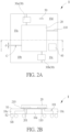
- FIG. 2A is a schematic diagram showing an exemplary semiconductor package in accordance with an embodiment of the invention.
- FIG. 2B is a cross-sectional view taken along line I-I' in FIG. 2A .
- the semiconductor package 1 comprises a partitioned package substrate 10 as set forth in FIG. 1 and at least one integrated circuit die 20 mounted on a first surface S1 of the partitioned package substrate 10.
- the first surface S1 of the partitioned package substrate 10 is a flat surface.
- the at least one integrated circuit die 20 may be mounted on the first surface S1 of the partitioned package substrate 10 in a flip-chip manner.
- the at least one integrated circuit die 20 is electrically connected to the partitioned package substrate 10 through a plurality of conductive elements 201 such as micro-bumps, copper bumps or copper pillars, but is not limited thereto.
- An underfill 210 may be filled into a space between the at least one integrated circuit die 20 and the first surface S1 of the partitioned package substrate 10.
- the partitioned package substrate 10 may have a square shape and a dimension of, for example, between 60 mm x 60mm and 70 mm x 70 mm.
- the partitioned package substrate 10 is composed of at least two smaller substrates (or smaller substrate blocks), for example, five coplanar small substrates 10a-10e, arranged in a side-by-side manner. It is to be understood that the number and shape of the substrates 10a-10d are for illustration purposes only.
- the central substrate 10e which may comprise a plurality of passive circuit elements including, but not limited to, integrated passive devices and/or deep trench capacitors, is situated directly under the at least one integrated circuit die 20.
- each of the four small substrates 10a-10e may have a rectangular shape and a dimension of, for example, 20 mm x 40mm.
- the central substrate 10e may have a square shape and a dimension of about 20 mm x 20mm.
- the four small substrates 10a-10d are rearranged and adjoined together with a gap Gtherebetween.
- the four small substrates 10a-10d may be adjoined or glued together side-by-side by using a gap-filling material 110 such as an adhesive or a molding compound that fills into the gap G.
- a gap-filling material 110 such as an adhesive or a molding compound that fills into the gap G.
- the width d of the gap G may range between 1-3 mm.
- the five small substrates 10a-10e may be homogeneous substrates.
- the five small substrates 10a-10e may be composed of substantially the same substrate materials such as BT substrates or ABF substrates.
- the five small substrates 10a-10e may be heterogeneous substrates.
- the five small substrates 10a-10e may be composed of substrate materials different from one another.
- the four small substrates 10a-10d may be composed of the same substrate material such as plastic or polymer, while the central substrate 10e is composed of a different substrate material such as silicon or ceramic.
- the five small substrates 10a-10e may have substantially the same thickness.
- the five small substrates 10a-10e may have different thicknesses.
- At least one of the five small substrates 10a-10e may comprise an interconnect structure 101 for electrically connecting the integrated circuit die 20 to the respective solder balls SB mounted on a second surface S2 of the partitioned package substrate 10.
- the interconnect structures 101 of the five small substrates 10a-10e may be the same as or similar to one another.
- the interconnect structures 101 of the five small substrates 10a-10e may be different from one another.
- the semiconductor package 1 may further comprise at least one die 30 mounted on the first surface S1 of the partitioned package substrate 10 in a flip-chip manner.
- the die 30 may overlap with at least two of the four small substrates 10a-10d.
- a die 30a is disposed between the small substrates 10a and 10d
- a die 30b is disposed between the small substrates 10b and 10c.
- the die 30 may be a dummy die that contains no active integrated circuit elements. The dummy die is used to bridge or interconnect the two adjacent small substrates.
- the die 30 may comprise a memory die such as a high bandwidth memory (HBM) die.
- HBM high bandwidth memory
- the semiconductor package 1 may further comprise an integrated circuit die 40 and an electronic device 50 such as a decoupling capacitor, an inductor, or a resistor mounted on the first surface S1 of the partitioned package substrate 10.
- the integrated circuit die 40 and the electronic device 50 may not overlap with the gap G.
- the partitioned package substrate 10 also improves the package warpage issues.
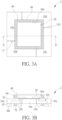
- FIG. 3A is a schematic diagram showing an exemplary semiconductor package in accordance with another embodiment of the invention, wherein like regions, layers or elements are designated by like numeral numbers or labels.
- FIG. 3B is a cross-sectional view taken along line II-II' in FIG. 3A .
- the semiconductor package 2 comprises a partitioned package substrate 10 and at least one integrated circuit die 20 mounted on a first surface S1 of the partitioned package substrate 10.
- the first surface S1 of the partitioned package substrate 10 is a flat surface.
- the at least one integrated circuit die 20 may be mounted on the first surface S1 of the partitioned package substrate 10 in a flip-chip manner.
- the at least one integrated circuit die 20 is electrically connected to the partitioned package substrate 10 through a plurality of conductive elements 201 such as micro-bumps, copper bumps or copper pillars, but is not limited thereto.
- the partitioned package substrate 10 may have a square shape and a dimension of, for example, between 60 mm x 60mm and 70 mm x 70 mm.
- the partitioned package substrate 10 is composed of at least two smaller substrates, for example, five coplanar small substrates 10a-10e, arranged in a side-by-side manner. It is to be understood that the number and shape of the substrates 10a-10d are for illustration purposes only.
- the central substrate 10e which may comprise a plurality of passive circuit elements including, but not limited to, integrated passive devices and/or deep trench capacitors, is situated directly under the at least one integrated circuit die 20.
- the five small substrates 10a-10e are physically separated from one another.
- each of the four small substrates 10a-10d may have a rectangular shape and a dimension of, for example, between 20 mm x 40 mm.
- the central substrate 10e may have a square shape and a dimension of, for example, between 20 mm x 20 mm.
- the five small substrates 10a-10e are rearranged and adjoined together with a gap G therebetween.
- the five small substrates 10a-10e may be adjoined or glued together side-by-side by using a gap-filling material 110 such as an adhesive or a molding compound that fills into the gap G.
- the width d of the gap G may range between 1-3 mm.
- the five small substrates 10a-10e may be homogeneous substrates.
- the five small substrates 10a-10e may be composed of substantially the same substrate materials such as BT substrates or ABF substrates.
- the five small substrates 10a-10e may be heterogeneous substrates.
- the five small substrates 10a-10e may be composed of substrate materials different from one another.
- the four small substrates 10a-10d may be composed of the same substrate material such as plastic or polymer, while the central substrate 10e is composed of a different substrate material such as silicon or ceramic.
- the five small substrates 10a-10e may have substantially the same thickness.
- the five small substrates 10a-10e may have different thicknesses.
- At least one of the five small substrates 10a-10e may comprise an interconnect structure 101 for electrically connecting the integrated circuit die 20 to the respective solder balls SB mounted on a second surface S2 of the partitioned package substrate 10.
- the interconnect structures 101 of the five small substrates 10a-10e may be the same as or similar to one another.
- the interconnect structures 101 of the five small substrates 10a-10e may be different from one another.
- the semiconductor package 2 may further comprise an annular frame 60 mounted on the first surface S1 of the partitioned package substrate 10.
- the semiconductor package 2 may further comprise an annular frame 70 mounted on the second surface S2 of the partitioned package substrate 10.
- the frames 60 and 70 may be a metal frame, but is not limited thereto.
- the frames 60 and 70 may be attached to the partitioned package substrate 10 by using joint bumps.
- the frames 60 and 70 may be attached to the partitioned package substrate 10 by using an adhesive.
- the frame 60 may comprise an opening 60a for accommodating the integrated circuit die 20.
- the integrated circuit die 20 may be surrounded by the frame 60.
- the semiconductor package 2 may further a mold cap 80.
- the mold cap 80 encapsulates the annular frame 60 and the at least one integrated circuit die 20.
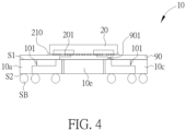
- FIG. 4 is a schematic, cross-sectional diagram showing another embodiment of the invention.
- a re-distribution layer (RDL) structure 90 may be disposed on the first surface S1 of the partitioned package substrate 10.
- the RDL structure 90 comprises interconnect 901.
- the integrated circuit die 20 is mounted on the RDL structure 90.
- the integrated circuit die 20 is electrically connected to the respective solder balls SB mounted on a second surface S2 of the partitioned package substrate 10 through the RDL structure 90 and the partitioned package substrate 10.
Landscapes
- Physics & Mathematics (AREA)
- Geometry (AREA)
- Combinations Of Printed Boards (AREA)
- Structures Or Materials For Encapsulating Or Coating Semiconductor Devices Or Solid State Devices (AREA)
Abstract
Description
- This application claims the benefit of
U.S. Provisional Application No. 63/369,979 - The present disclosure relates generally to the field of semiconductor packaging. More particularly, the present disclosure relates to a cost-effective, large-die semiconductor package using substrate block integration (SBI).
- As more consumers embrace smart devices, demand grows for networking data centers, Internet of Things, smart sensors, etc. To meet these needs, semiconductor design companies are encountering challenges in chip design complexity and PPA (power, performance, area) factors in lower geometries, such as 7 nm, 5 nm, and 3 nm.
- Advanced packaging is playing a bigger role across the semiconductor industry. Networking equipment, servers, and smartphones are among the applications that have adopted advanced packaging. To advance a design, IC vendors develop an ASIC. Then, vendors will shrink different functions at each node and pack them onto the ASIC. But this approach is becoming more complex and expensive at each node.
- For example, an ASIC for switch routers or data centers may include a large die and the size of the package may typically exceed 4500 mm2, which leads to a rising cost of the ASIC package because of the low production yield of the package substrate at this size. The ASIC package with large die also encounters warpage problems.
- It is one object of the present disclosure to provide an improved large-die semiconductor package using substrate block integration (SBI) in order to solve the prior art shortcomings or deficiencies. A semiconductor package according to the invention is defined in
independent claim 1. The dependent claims define preferred embodiments thereof. - One aspect of the invention provides a semiconductor package including a partitioned package substrate composed of discrete substrates arranged in a side-by-side manner. The discrete substrates comprise a central substrate and peripheral substrates surrounding the central substrate. At least one integrated circuit die is mounted on a first surface of the partitioned package substrate. A plurality of solder balls is mounted on a second surface of the partitioned package substrate opposite to the first surface.
- Preferably, the at least one integrated circuit die is electrically connected to the partitioned package substrate through a plurality of conductive elements.
- Preferably, the conductive elements comprise micro-bumps, copper bumps or copper pillars.
- Preferably, the discrete substrates are physically separated from one another.
- Preferably, the discrete substrates are rearranged and adjoined together with a gap therebetween.
- Preferably, the discrete substrates are adjoined together by using an adhesive that fills into the gap.
- Preferably, the gap has a width ranging between 1-3 mm.
- Preferably, the discrete substrates are homogeneous substrates.
- Preferably, the discrete substrates are heterogeneous substrates.
- Preferably, the discrete substrates have the same thickness.
- Preferably, the discrete substrates have different thicknesses.
- Preferably, the semiconductor package further includes at least one die mounted on the first surface of the partitioned package substrate in a flip-chip manner.
- Preferably, the at least one die is a dummy die.
- Preferably, the at least one die is a memory die.
- Preferably, the semiconductor package further includes a second integrated circuit die; and an electronic device mounted on the first surface of the partitioned package substrate.
- Preferably, the electronic device comprises a decoupling capacitor.
- Preferably, the second integrated circuit die and the electronic device do not overlap with the gap.
- Preferably, the semiconductor package further includes an annular frame mounted on the first surface of the partitioned package substrate.
- Preferably, the annular frame is a metal frame.
- Preferably, the annular frame is attached to the first surface of the partitioned package substrate by using joint bumps.
- Preferably, the annular frame is attached to the first surface of the partitioned package substrate by using adhesive.
- Preferably, the annular frame comprise an opening for accommodating the at least one integrated circuit die.
- Preferably, the semiconductor package further includes a mold cap encapsulating the at least one integrated circuit die and the annular frame.
- Preferably, the semiconductor package further includes a re-distribution layer (RDL) structure on the first surface of the partitioned package substrate, wherein the at least one integrated circuit die is mounted on the RDL structure.
- Preferably, the central substrate is a silicon substrate and comprises passive circuit elements including integrated passive devices or deep trench capacitors.
- Preferably, the central substrate is a ceramic substrate and comprises multi-layer ceramic capacitors.
- These and other objectives of the present invention will no doubt become obvious to those of ordinary skill in the art after reading the following detailed description of the preferred embodiment that is illustrated in the various figures and drawings.
- The accompanying drawings are included to provide a further understanding of the invention and are incorporated in and constitute a part of this specification. The drawings illustrate embodiments of the invention and, together with the description, serve to explain the principles of the invention. In the drawings:
-
FIG. 1 is a schematic diagram showing an exemplary partitioned package substrate in accordance with an embodiment of the invention; -
FIG. 2A is a schematic diagram showing an exemplary semiconductor package in accordance with an embodiment of the invention; -
FIG. 2B is a cross-sectional view taken along line I-I' inFIG. 2A ; -
FIG. 3A is a schematic diagram showing an exemplary semiconductor package in accordance with another embodiment of the invention; -
FIG. 3B is a cross-sectional view taken along line II-II' inFIG. 3A ; and -
FIG. 4 is a schematic, cross-sectional diagram showing another embodiment of the invention. - In the following detailed description of embodiments of the invention, reference is made to the accompanying drawings, which form a part hereof, and in which is shown by way of illustration specific preferred embodiments in which the disclosure may be practiced.
- These embodiments are described in sufficient detail to enable those skilled in the art to practice them, and it is to be understood that other embodiments may be utilized and that mechanical, chemical, electrical, and procedural changes may be made without departing from the scope of the present disclosure. The following detailed description is, therefore, not to be taken in a limiting sense, and the scope of embodiments of the present invention is defined only by the appended claims.
- It will be understood that when an element or layer is referred to as being "on", "connected to" or "coupled to" another element or layer, it can be directly on, connected or coupled to the other element or layer or intervening elements or layers may be present. In contrast, when an element is referred to as being "directly on," "directly connected to" or "directly coupled to" another element or layer, there are no intervening elements or layers present. Like numbers refer to like elements throughout. As used herein, the term "and/or" includes any and all combinations of one or more of the associated listed items.
- Please refer to
FIG. 1. FIG. 1 is a schematic diagram showing an exemplary partitioned package substrate in accordance with an embodiment of the invention. As shown inFIG. 1 , the partitionedpackage substrate 10 is composed of at least two smaller substrates (or smaller substrate blocks) arranged in a side-by-side manner. For example, five coplanarsmall substrates 10a-10e are demonstrated inFIG. 1 . It is to be understood that the number and shape of thesubstrates 10a-10e are for illustration purposes only. Preferably, the partitionedpackage substrate 10 may have a square shape and a dimension of, for example, between 60 mm x 60mm and 70 mm x 70 mm. - Preferably, the five
small substrates 10a-10e are physically separated from one another. The fivediscrete substrates 10a-10e include acentral substrate 10e and four rectangular shapedperipheral substrates 10a-10d surrounding thecentral substrate 10e. Thecentral substrate 10e is surrounded by the foursubstrates 10a-10d. Preferably, for example, each of the foursmall substrates 10a-10d may have a rectangular shape and a dimension of about 20 mm x 40mm. Preferably, for example, thecentral substrate 10e may have a square shape and a dimension of about 20 mm x 20mm. - Preferably, the five
small substrates 10a-10e are rearranged and adjoined together with a gap Gtherebetween. Preferably, for example, the foursmall substrates 10a-10d may be adjoined or glued together side-by-side by using a gap-fillingmaterial 110 such as an adhesive or a molding compound that fills into the gap G. Preferably, for example, the gap G may have a width d ranging between 1-3 mm. - Preferably, the five
small substrates 10a-10e may be homogeneous substrates. For example, the fivesmall substrates 10a-10e may be composed of substantially the same substrate materials such as BT substrates or ABF substrates. According to another embodiment of the invention, the fivesmall substrates 10a-10e may be heterogeneous substrates. For example, the fivesmall substrates 10a-10e may be composed of different substrate materials such as glass substrates, ceramic substrates, BT substrates, ABF substrates, etc. Preferably, thecentral substrate 10e may be a silicon substrate and may comprise a plurality of passive circuit elements including, but not limited to, integrated passive devices and/or deep trench capacitors. Preferably, thecentral substrate 10e may be a ceramic substrate and may comprise a plurality of multi-layer ceramic capacitors (MLCC). - Preferably, the five
small substrates 10a-10e may have substantially the same thickness. Preferably, the fivesmall substrates 10a-10e may have different thicknesses. - Please refer to
FIG. 2A and FIG. 2B. FIG. 2A is a schematic diagram showing an exemplary semiconductor package in accordance with an embodiment of the invention.FIG. 2B is a cross-sectional view taken along line I-I' inFIG. 2A . As shown inFIG. 2A and FIG. 2B , thesemiconductor package 1 comprises a partitionedpackage substrate 10 as set forth inFIG. 1 and at least one integrated circuit die 20 mounted on a first surface S1 of the partitionedpackage substrate 10. Preferably, the first surface S1 of the partitionedpackage substrate 10 is a flat surface. Preferably, for example, the at least one integrated circuit die 20 may be mounted on the first surface S1 of the partitionedpackage substrate 10 in a flip-chip manner. Preferably, the at least one integrated circuit die 20 is electrically connected to the partitionedpackage substrate 10 through a plurality ofconductive elements 201 such as micro-bumps, copper bumps or copper pillars, but is not limited thereto. Anunderfill 210 may be filled into a space between the at least one integrated circuit die 20 and the first surface S1 of the partitionedpackage substrate 10. Preferably, the partitionedpackage substrate 10 may have a square shape and a dimension of, for example, between 60 mm x 60mm and 70 mm x 70 mm. - Preferably, the partitioned
package substrate 10 is composed of at least two smaller substrates (or smaller substrate blocks), for example, five coplanarsmall substrates 10a-10e, arranged in a side-by-side manner. It is to be understood that the number and shape of thesubstrates 10a-10d are for illustration purposes only. Preferably, thecentral substrate 10e, which may comprise a plurality of passive circuit elements including, but not limited to, integrated passive devices and/or deep trench capacitors, is situated directly under the at least one integrated circuit die 20. - Preferably, the five
small substrates 10a-10e are physically separated from one another. Preferably, each of the foursmall substrates 10a-10d may have a rectangular shape and a dimension of, for example, 20 mm x 40mm. Preferably, for example, thecentral substrate 10e may have a square shape and a dimension of about 20 mm x 20mm. - Preferably, the four
small substrates 10a-10d are rearranged and adjoined together with a gap Gtherebetween. Preferably, for example, the foursmall substrates 10a-10d may be adjoined or glued together side-by-side by using a gap-fillingmaterial 110 such as an adhesive or a molding compound that fills into the gap G. Preferably, for example, the width d of the gap G may range between 1-3 mm. - Preferably, the five
small substrates 10a-10e may be homogeneous substrates. For example, the fivesmall substrates 10a-10e may be composed of substantially the same substrate materials such as BT substrates or ABF substrates. According to another embodiment of the invention, the fivesmall substrates 10a-10e may be heterogeneous substrates. For example, the fivesmall substrates 10a-10e may be composed of substrate materials different from one another. For example, the foursmall substrates 10a-10d may be composed of the same substrate material such as plastic or polymer, while thecentral substrate 10e is composed of a different substrate material such as silicon or ceramic. Preferably, the fivesmall substrates 10a-10e may have substantially the same thickness. Preferably, the fivesmall substrates 10a-10e may have different thicknesses. - Preferably, at least one of the five
small substrates 10a-10e may comprise aninterconnect structure 101 for electrically connecting the integrated circuit die 20 to the respective solder balls SB mounted on a second surface S2 of the partitionedpackage substrate 10. Preferably, theinterconnect structures 101 of the fivesmall substrates 10a-10e may be the same as or similar to one another. Preferably, theinterconnect structures 101 of the fivesmall substrates 10a-10e may be different from one another. - Preferably, the
semiconductor package 1 may further comprise at least one die 30 mounted on the first surface S1 of the partitionedpackage substrate 10 in a flip-chip manner. Preferably, thedie 30 may overlap with at least two of the foursmall substrates 10a-10d. For example, inFIG. 2A , adie 30a is disposed between thesmall substrates die 30b is disposed between thesmall substrates die 30 may be a dummy die that contains no active integrated circuit elements. The dummy die is used to bridge or interconnect the two adjacent small substrates. According to another embodiment of the invention, thedie 30 may comprise a memory die such as a high bandwidth memory (HBM) die. - Preferably, the
semiconductor package 1 may further comprise an integrated circuit die 40 and anelectronic device 50 such as a decoupling capacitor, an inductor, or a resistor mounted on the first surface S1 of the partitionedpackage substrate 10. The integrated circuit die 40 and theelectronic device 50 may not overlap with the gap G. - By adopting smaller substrates, the reliability and the design flexibility of the semiconductor package structure can be improved and the production cost can be reduced. The partitioned
package substrate 10 also improves the package warpage issues. - Please refer to
FIG. 3A and FIG. 3B. FIG. 3A is a schematic diagram showing an exemplary semiconductor package in accordance with another embodiment of the invention, wherein like regions, layers or elements are designated by like numeral numbers or labels.FIG. 3B is a cross-sectional view taken along line II-II' inFIG. 3A . As shown inFIG. 3A and FIG. 3B , likewise, thesemiconductor package 2 comprises a partitionedpackage substrate 10 and at least one integrated circuit die 20 mounted on a first surface S1 of the partitionedpackage substrate 10. Preferably, the first surface S1 of the partitionedpackage substrate 10 is a flat surface. Preferably, for example, the at least one integrated circuit die 20 may be mounted on the first surface S1 of the partitionedpackage substrate 10 in a flip-chip manner. Preferably, the at least one integrated circuit die 20 is electrically connected to the partitionedpackage substrate 10 through a plurality ofconductive elements 201 such as micro-bumps, copper bumps or copper pillars, but is not limited thereto. Preferably, the partitionedpackage substrate 10 may have a square shape and a dimension of, for example, between 60 mm x 60mm and 70 mm x 70 mm. - Preferably, the partitioned
package substrate 10 is composed of at least two smaller substrates, for example, five coplanarsmall substrates 10a-10e, arranged in a side-by-side manner. It is to be understood that the number and shape of thesubstrates 10a-10d are for illustration purposes only. Preferably, thecentral substrate 10e, which may comprise a plurality of passive circuit elements including, but not limited to, integrated passive devices and/or deep trench capacitors, is situated directly under the at least one integrated circuit die 20. - Preferably, the five
small substrates 10a-10e are physically separated from one another. Preferably, each of the foursmall substrates 10a-10d may have a rectangular shape and a dimension of, for example, between 20 mm x 40 mm. Preferably, thecentral substrate 10e may have a square shape and a dimension of, for example, between 20 mm x 20 mm. Preferably, the fivesmall substrates 10a-10e are rearranged and adjoined together with a gap G therebetween. Preferably, for example, the fivesmall substrates 10a-10e may be adjoined or glued together side-by-side by using a gap-fillingmaterial 110 such as an adhesive or a molding compound that fills into the gap G. Preferably, for example, the width d of the gap G may range between 1-3 mm. - Preferably, the five
small substrates 10a-10e may be homogeneous substrates. For example, the fivesmall substrates 10a-10e may be composed of substantially the same substrate materials such as BT substrates or ABF substrates. According to another embodiment of the invention, the fivesmall substrates 10a-10e may be heterogeneous substrates. For example, the fivesmall substrates 10a-10e may be composed of substrate materials different from one another. For example, the foursmall substrates 10a-10d may be composed of the same substrate material such as plastic or polymer, while thecentral substrate 10e is composed of a different substrate material such as silicon or ceramic. Preferably, the fivesmall substrates 10a-10e may have substantially the same thickness. Preferably, the fivesmall substrates 10a-10e may have different thicknesses. - Preferably, at least one of the five
small substrates 10a-10e may comprise aninterconnect structure 101 for electrically connecting the integrated circuit die 20 to the respective solder balls SB mounted on a second surface S2 of the partitionedpackage substrate 10. Preferably, theinterconnect structures 101 of the fivesmall substrates 10a-10e may be the same as or similar to one another. Preferably, theinterconnect structures 101 of the fivesmall substrates 10a-10e may be different from one another. - Preferably, the
semiconductor package 2 may further comprise anannular frame 60 mounted on the first surface S1 of the partitionedpackage substrate 10. According to another embodiment of the invention, optionally, thesemiconductor package 2 may further comprise anannular frame 70 mounted on the second surface S2 of the partitionedpackage substrate 10. Preferably, theframes frames package substrate 10 by using joint bumps. Preferably, theframes package substrate 10 by using an adhesive. Theframe 60 may comprise anopening 60a for accommodating the integrated circuit die 20. The integrated circuit die 20 may be surrounded by theframe 60. Preferably, thesemiconductor package 2 may further amold cap 80. Preferably, themold cap 80 encapsulates theannular frame 60 and the at least one integrated circuit die 20. - Please refer to
FIG. 4. FIG. 4 is a schematic, cross-sectional diagram showing another embodiment of the invention. As shown inFIG. 4 , a re-distribution layer (RDL)structure 90 may be disposed on the first surface S1 of the partitionedpackage substrate 10. Preferably, theRDL structure 90 comprisesinterconnect 901. The integrated circuit die 20 is mounted on theRDL structure 90. The integrated circuit die 20 is electrically connected to the respective solder balls SB mounted on a second surface S2 of the partitionedpackage substrate 10 through theRDL structure 90 and the partitionedpackage substrate 10. - Those skilled in the art will readily observe that numerous modifications and alterations of the device and method may be made while retaining the teachings of the invention. Accordingly, the above disclosure should be construed as limited only by the metes and bounds of the appended claims.
Claims (15)
- A semiconductor package (1; 2), comprising:a partitioned package substrate (10) composed of a plurality of discrete substrates (10a - 10e) arranged in a side-by-side manner, wherein the plurality of discrete substrates (10a - 10e) comprises a central substrate (10e) and peripheral substrates (10a, 10b, 10c, 10d) surrounding the central substrate (10e);at least one integrated circuit die (20) mounted on a first surface (S1) of the partitioned package substrate (10); anda plurality of solder balls (SB) mounted on a second surface (S2) of the partitioned package substrate (10) opposite to the first surface (S1).
- The semiconductor package (1; 2) according to claim 1, wherein the at least one integrated circuit die (20) is electrically connected to the partitioned package substrate (10) through a plurality of conductive elements (201).
- The semiconductor package (1; 2) according to claim 2, wherein the conductive elements (201) comprise micro-bumps, copper bumps or copper pillars.
- The semiconductor package (1; 2) according to claim 1, wherein the plurality of discrete substrates (10a - 10e) are physically separated from one another.
- The semiconductor package (1; 2) according to claim 1, wherein the plurality of discrete substrates (10a - 10e) are rearranged and adjoined together with a gap (G) therebetween.
- The semiconductor package (1; 2) according to claim 5, wherein the plurality of discrete substrates (10a - 10e) are adjoined together by using an adhesive (110) that fills into the gap (G); and/or
wherein the gap (G) has a width (d) ranging between 1-3 mm. - The semiconductor package (1; 2) according to any one of claims 1 to 6, wherein the plurality of discrete substrates (10a - 10e) are homogeneous substrates or heterogeneous substrates; and/or
wherein the plurality of discrete substrates (10a - 10e) have the same thickness or have different thicknesses. - The semiconductor package (1; 2) according to any one of claims 1 to 7, further comprising:
at least one die (30) mounted on the first surface (S1) of the partitioned package substrate (10) in a flip-chip manner. - The semiconductor package (1; 2) according to claim 8, wherein the at least one die (30) is a dummy die or a memory die.
- The semiconductor package (1; 2) according to claim 5 or 6, or any one of claims 7 to 9 in combination with claim 5 or 6, further comprising:a second integrated circuit die (40); andan electronic device (50) mounted on the first surface (S1) of the partitioned package substrate (10).
- The semiconductor package (1; 2) according to claim 10, wherein the electronic device (50) comprises a decoupling capacitor; and/or
wherein the second integrated circuit die (40) and the electronic device (50) do not overlap with the gap (G). - The semiconductor package (2) according to any one of claims 1 to 11, further comprising:
an annular frame (60) mounted on the first surface (S1) of the partitioned package substrate (10). - The semiconductor package (2) according to claim 12, wherein the annular frame (60) is a metal frame; and/orwherein the annular frame (60) is attached to the first surface (S1) of the partitioned package substrate (10) by using joint bumps; and/orwherein the annular frame (60) is attached to the first surface (S1) of the partitioned package substrate (10) by using adhesive; and/orwherein the annular frame (60) comprise an opening (60a) for accommodating the at least one integrated circuit die (20); and/orfurther comprising:
a mold cap (80) encapsulating the at least one integrated circuit die (20) and the annular frame (60). - The semiconductor package (1; 2) according to any one of claims 1 to 13, further comprising:
a re-distribution layer, in the following also referred to as RDL, structure (90) on the first surface (S1) of the partitioned package substrate (10), wherein the at least one integrated circuit die (20) is mounted on the RDL structure (90). - The semiconductor package (1; 2) according to any one of claims 1 to 14, wherein the central substrate (10e) is a silicon substrate and comprises a plurality of passive circuit elements comprising integrated passive devices or deep trench capacitors; or
wherein the central substrate (10e) is a ceramic substrate and comprises a plurality of multi-layer ceramic capacitors.
Applications Claiming Priority (2)
| Application Number | Priority Date | Filing Date | Title |
|---|---|---|---|
| US202263369979P | 2022-08-01 | 2022-08-01 | |
| US18/216,561 US12622332B2 (en) | 2022-08-01 | 2023-06-29 | Semiconductor package using substrate block integration |
Publications (1)
| Publication Number | Publication Date |
|---|---|
| EP4322206A1 true EP4322206A1 (en) | 2024-02-14 |
Family
ID=87378050
Family Applications (1)
| Application Number | Title | Priority Date | Filing Date |
|---|---|---|---|
| EP23185518.0A Pending EP4322206A1 (en) | 2022-08-01 | 2023-07-14 | Semiconductor package using substrate block integration |
Country Status (2)
| Country | Link |
|---|---|
| US (1) | US12622332B2 (en) |
| EP (1) | EP4322206A1 (en) |
Citations (2)
| Publication number | Priority date | Publication date | Assignee | Title |
|---|---|---|---|---|
| WO2013095544A1 (en) * | 2011-12-22 | 2013-06-27 | Intel Corporation | 3d integrated circuit package with window interposer |
| US20210159211A1 (en) * | 2019-11-27 | 2021-05-27 | International Business Machines Corporation | Multi-chip package structures formed by joining chips to pre-positioned chip interconnect bridge devices |
Family Cites Families (1)
| Publication number | Priority date | Publication date | Assignee | Title |
|---|---|---|---|---|
| US11282806B2 (en) * | 2019-10-11 | 2022-03-22 | Marvell Asia Pte, Ltd. | Partitioned substrates with interconnect bridge |
-
2023
- 2023-06-29 US US18/216,561 patent/US12622332B2/en active Active
- 2023-07-14 EP EP23185518.0A patent/EP4322206A1/en active Pending
Patent Citations (2)
| Publication number | Priority date | Publication date | Assignee | Title |
|---|---|---|---|---|
| WO2013095544A1 (en) * | 2011-12-22 | 2013-06-27 | Intel Corporation | 3d integrated circuit package with window interposer |
| US20210159211A1 (en) * | 2019-11-27 | 2021-05-27 | International Business Machines Corporation | Multi-chip package structures formed by joining chips to pre-positioned chip interconnect bridge devices |
Also Published As
| Publication number | Publication date |
|---|---|
| US12622332B2 (en) | 2026-05-05 |
| US20240038648A1 (en) | 2024-02-01 |
Similar Documents
| Publication | Publication Date | Title |
|---|---|---|
| KR102845418B1 (en) | Partitioned substrates with interconnect bridge | |
| KR101809521B1 (en) | Semiconductor package and method of manufacturing the same | |
| KR20080020069A (en) | Semiconductor package and manufacturing method | |
| US9881902B2 (en) | Semiconductor package, semiconductor device using the same and manufacturing method thereof | |
| CN114023663A (en) | Three-dimensional board-level fan-out type packaging structure and manufacturing method thereof | |
| CN112701101B (en) | Electronic packaging and method of manufacturing the same | |
| US10497678B2 (en) | Semiconductor package assembly with passive device | |
| CN118039572A (en) | Electronic packaging and method of manufacturing the same | |
| US12119296B2 (en) | Encircling a semiconductor device with stacked frames on a substrate | |
| KR20110105159A (en) | Laminated Semiconductor Package and Formation Method | |
| US9799637B2 (en) | Semiconductor package with lid having lid conductive structure | |
| US11967559B2 (en) | Electronic package | |
| CN115312490B (en) | Electronic module, manufacturing method thereof and electronic package | |
| US12622332B2 (en) | Semiconductor package using substrate block integration | |
| US10515883B2 (en) | 3D system-level packaging methods and structures | |
| EP4318580A1 (en) | Semiconductor package using substrate block integration | |
| US8012800B2 (en) | Method of fabricating a stacked type chip package structure and a stacked type package structure | |
| US9041221B2 (en) | Electronic component implementing structure intermediate body, electronic component implementing structure body and manufacturing method of electronic component implementing structure body | |
| CN117497507A (en) | Semiconductor packaging | |
| CN220457668U (en) | Packaging module comprising multilayer circuit board and electronic equipment | |
| US20250246580A1 (en) | Integrated circuit die stack with a bridge die | |
| KR101819558B1 (en) | Semiconductor package and method of manufacturing the same | |
| US20250246519A1 (en) | Integrated circuit die stack with a dual-sided bridge die | |
| US20240347479A1 (en) | Semiconductor package having moisture passing gap in power or ground metal plane of a package substrate | |
| US20190055118A1 (en) | Mems device package and method for manufacturing the same |
Legal Events
| Date | Code | Title | Description |
|---|---|---|---|
| PUAI | Public reference made under article 153(3) epc to a published international application that has entered the european phase |
Free format text: ORIGINAL CODE: 0009012 |
|
| STAA | Information on the status of an ep patent application or granted ep patent |
Free format text: STATUS: THE APPLICATION HAS BEEN PUBLISHED |
|
| AK | Designated contracting states |
Kind code of ref document: A1 Designated state(s): AL AT BE BG CH CY CZ DE DK EE ES FI FR GB GR HR HU IE IS IT LI LT LU LV MC ME MK MT NL NO PL PT RO RS SE SI SK SM TR |
|
| STAA | Information on the status of an ep patent application or granted ep patent |
Free format text: STATUS: REQUEST FOR EXAMINATION WAS MADE |
|
| 17P | Request for examination filed |
Effective date: 20240809 |
|
| RBV | Designated contracting states (corrected) |
Designated state(s): AL AT BE BG CH CY CZ DE DK EE ES FI FR GB GR HR HU IE IS IT LI LT LU LV MC ME MK MT NL NO PL PT RO RS SE SI SK SM TR |