EP4322147A1 - Driving circuit, display module, and display device - Google Patents
Driving circuit, display module, and display device Download PDFInfo
- Publication number
- EP4322147A1 EP4322147A1 EP22930178.3A EP22930178A EP4322147A1 EP 4322147 A1 EP4322147 A1 EP 4322147A1 EP 22930178 A EP22930178 A EP 22930178A EP 4322147 A1 EP4322147 A1 EP 4322147A1
- Authority
- EP
- European Patent Office
- Prior art keywords
- transistor
- signal
- display
- receive
- comparator
- Prior art date
- Legal status (The legal status is an assumption and is not a legal conclusion. Google has not performed a legal analysis and makes no representation as to the accuracy of the status listed.)
- Pending
Links
Images


Classifications
-
- G—PHYSICS
- G09—EDUCATION; CRYPTOGRAPHY; DISPLAY; ADVERTISING; SEALS
- G09G—ARRANGEMENTS OR CIRCUITS FOR CONTROL OF INDICATING DEVICES USING STATIC MEANS TO PRESENT VARIABLE INFORMATION
- G09G3/00—Control arrangements or circuits, of interest only in connection with visual indicators other than cathode-ray tubes
- G09G3/20—Control arrangements or circuits, of interest only in connection with visual indicators other than cathode-ray tubes for presentation of an assembly of a number of characters, e.g. a page, by composing the assembly by combination of individual elements arranged in a matrix no fixed position being assigned to or needed to be assigned to the individual characters or partial characters
- G09G3/22—Control arrangements or circuits, of interest only in connection with visual indicators other than cathode-ray tubes for presentation of an assembly of a number of characters, e.g. a page, by composing the assembly by combination of individual elements arranged in a matrix no fixed position being assigned to or needed to be assigned to the individual characters or partial characters using controlled light sources
- G09G3/30—Control arrangements or circuits, of interest only in connection with visual indicators other than cathode-ray tubes for presentation of an assembly of a number of characters, e.g. a page, by composing the assembly by combination of individual elements arranged in a matrix no fixed position being assigned to or needed to be assigned to the individual characters or partial characters using controlled light sources using electroluminescent panels
- G09G3/32—Control arrangements or circuits, of interest only in connection with visual indicators other than cathode-ray tubes for presentation of an assembly of a number of characters, e.g. a page, by composing the assembly by combination of individual elements arranged in a matrix no fixed position being assigned to or needed to be assigned to the individual characters or partial characters using controlled light sources using electroluminescent panels semiconductive, e.g. using light-emitting diodes [LED]
- G09G3/3208—Control arrangements or circuits, of interest only in connection with visual indicators other than cathode-ray tubes for presentation of an assembly of a number of characters, e.g. a page, by composing the assembly by combination of individual elements arranged in a matrix no fixed position being assigned to or needed to be assigned to the individual characters or partial characters using controlled light sources using electroluminescent panels semiconductive, e.g. using light-emitting diodes [LED] organic, e.g. using organic light-emitting diodes [OLED]
- G09G3/3225—Control arrangements or circuits, of interest only in connection with visual indicators other than cathode-ray tubes for presentation of an assembly of a number of characters, e.g. a page, by composing the assembly by combination of individual elements arranged in a matrix no fixed position being assigned to or needed to be assigned to the individual characters or partial characters using controlled light sources using electroluminescent panels semiconductive, e.g. using light-emitting diodes [LED] organic, e.g. using organic light-emitting diodes [OLED] using an active matrix
-
- G—PHYSICS
- G09—EDUCATION; CRYPTOGRAPHY; DISPLAY; ADVERTISING; SEALS
- G09G—ARRANGEMENTS OR CIRCUITS FOR CONTROL OF INDICATING DEVICES USING STATIC MEANS TO PRESENT VARIABLE INFORMATION
- G09G3/00—Control arrangements or circuits, of interest only in connection with visual indicators other than cathode-ray tubes
- G09G3/20—Control arrangements or circuits, of interest only in connection with visual indicators other than cathode-ray tubes for presentation of an assembly of a number of characters, e.g. a page, by composing the assembly by combination of individual elements arranged in a matrix no fixed position being assigned to or needed to be assigned to the individual characters or partial characters
- G09G3/22—Control arrangements or circuits, of interest only in connection with visual indicators other than cathode-ray tubes for presentation of an assembly of a number of characters, e.g. a page, by composing the assembly by combination of individual elements arranged in a matrix no fixed position being assigned to or needed to be assigned to the individual characters or partial characters using controlled light sources
- G09G3/30—Control arrangements or circuits, of interest only in connection with visual indicators other than cathode-ray tubes for presentation of an assembly of a number of characters, e.g. a page, by composing the assembly by combination of individual elements arranged in a matrix no fixed position being assigned to or needed to be assigned to the individual characters or partial characters using controlled light sources using electroluminescent panels
- G09G3/32—Control arrangements or circuits, of interest only in connection with visual indicators other than cathode-ray tubes for presentation of an assembly of a number of characters, e.g. a page, by composing the assembly by combination of individual elements arranged in a matrix no fixed position being assigned to or needed to be assigned to the individual characters or partial characters using controlled light sources using electroluminescent panels semiconductive, e.g. using light-emitting diodes [LED]
- G09G3/3208—Control arrangements or circuits, of interest only in connection with visual indicators other than cathode-ray tubes for presentation of an assembly of a number of characters, e.g. a page, by composing the assembly by combination of individual elements arranged in a matrix no fixed position being assigned to or needed to be assigned to the individual characters or partial characters using controlled light sources using electroluminescent panels semiconductive, e.g. using light-emitting diodes [LED] organic, e.g. using organic light-emitting diodes [OLED]
- G09G3/3266—Details of drivers for scan electrodes
-
- G—PHYSICS
- G09—EDUCATION; CRYPTOGRAPHY; DISPLAY; ADVERTISING; SEALS
- G09G—ARRANGEMENTS OR CIRCUITS FOR CONTROL OF INDICATING DEVICES USING STATIC MEANS TO PRESENT VARIABLE INFORMATION
- G09G3/00—Control arrangements or circuits, of interest only in connection with visual indicators other than cathode-ray tubes
- G09G3/20—Control arrangements or circuits, of interest only in connection with visual indicators other than cathode-ray tubes for presentation of an assembly of a number of characters, e.g. a page, by composing the assembly by combination of individual elements arranged in a matrix no fixed position being assigned to or needed to be assigned to the individual characters or partial characters
- G09G3/22—Control arrangements or circuits, of interest only in connection with visual indicators other than cathode-ray tubes for presentation of an assembly of a number of characters, e.g. a page, by composing the assembly by combination of individual elements arranged in a matrix no fixed position being assigned to or needed to be assigned to the individual characters or partial characters using controlled light sources
- G09G3/30—Control arrangements or circuits, of interest only in connection with visual indicators other than cathode-ray tubes for presentation of an assembly of a number of characters, e.g. a page, by composing the assembly by combination of individual elements arranged in a matrix no fixed position being assigned to or needed to be assigned to the individual characters or partial characters using controlled light sources using electroluminescent panels
- G09G3/32—Control arrangements or circuits, of interest only in connection with visual indicators other than cathode-ray tubes for presentation of an assembly of a number of characters, e.g. a page, by composing the assembly by combination of individual elements arranged in a matrix no fixed position being assigned to or needed to be assigned to the individual characters or partial characters using controlled light sources using electroluminescent panels semiconductive, e.g. using light-emitting diodes [LED]
- G09G3/3208—Control arrangements or circuits, of interest only in connection with visual indicators other than cathode-ray tubes for presentation of an assembly of a number of characters, e.g. a page, by composing the assembly by combination of individual elements arranged in a matrix no fixed position being assigned to or needed to be assigned to the individual characters or partial characters using controlled light sources using electroluminescent panels semiconductive, e.g. using light-emitting diodes [LED] organic, e.g. using organic light-emitting diodes [OLED]
-
- G—PHYSICS
- G09—EDUCATION; CRYPTOGRAPHY; DISPLAY; ADVERTISING; SEALS
- G09G—ARRANGEMENTS OR CIRCUITS FOR CONTROL OF INDICATING DEVICES USING STATIC MEANS TO PRESENT VARIABLE INFORMATION
- G09G3/00—Control arrangements or circuits, of interest only in connection with visual indicators other than cathode-ray tubes
- G09G3/20—Control arrangements or circuits, of interest only in connection with visual indicators other than cathode-ray tubes for presentation of an assembly of a number of characters, e.g. a page, by composing the assembly by combination of individual elements arranged in a matrix no fixed position being assigned to or needed to be assigned to the individual characters or partial characters
- G09G3/22—Control arrangements or circuits, of interest only in connection with visual indicators other than cathode-ray tubes for presentation of an assembly of a number of characters, e.g. a page, by composing the assembly by combination of individual elements arranged in a matrix no fixed position being assigned to or needed to be assigned to the individual characters or partial characters using controlled light sources
- G09G3/30—Control arrangements or circuits, of interest only in connection with visual indicators other than cathode-ray tubes for presentation of an assembly of a number of characters, e.g. a page, by composing the assembly by combination of individual elements arranged in a matrix no fixed position being assigned to or needed to be assigned to the individual characters or partial characters using controlled light sources using electroluminescent panels
- G09G3/32—Control arrangements or circuits, of interest only in connection with visual indicators other than cathode-ray tubes for presentation of an assembly of a number of characters, e.g. a page, by composing the assembly by combination of individual elements arranged in a matrix no fixed position being assigned to or needed to be assigned to the individual characters or partial characters using controlled light sources using electroluminescent panels semiconductive, e.g. using light-emitting diodes [LED]
- G09G3/3208—Control arrangements or circuits, of interest only in connection with visual indicators other than cathode-ray tubes for presentation of an assembly of a number of characters, e.g. a page, by composing the assembly by combination of individual elements arranged in a matrix no fixed position being assigned to or needed to be assigned to the individual characters or partial characters using controlled light sources using electroluminescent panels semiconductive, e.g. using light-emitting diodes [LED] organic, e.g. using organic light-emitting diodes [OLED]
- G09G3/3225—Control arrangements or circuits, of interest only in connection with visual indicators other than cathode-ray tubes for presentation of an assembly of a number of characters, e.g. a page, by composing the assembly by combination of individual elements arranged in a matrix no fixed position being assigned to or needed to be assigned to the individual characters or partial characters using controlled light sources using electroluminescent panels semiconductive, e.g. using light-emitting diodes [LED] organic, e.g. using organic light-emitting diodes [OLED] using an active matrix
- G09G3/3233—Control arrangements or circuits, of interest only in connection with visual indicators other than cathode-ray tubes for presentation of an assembly of a number of characters, e.g. a page, by composing the assembly by combination of individual elements arranged in a matrix no fixed position being assigned to or needed to be assigned to the individual characters or partial characters using controlled light sources using electroluminescent panels semiconductive, e.g. using light-emitting diodes [LED] organic, e.g. using organic light-emitting diodes [OLED] using an active matrix with pixel circuitry controlling the current through the light-emitting element
-
- G—PHYSICS
- G09—EDUCATION; CRYPTOGRAPHY; DISPLAY; ADVERTISING; SEALS
- G09G—ARRANGEMENTS OR CIRCUITS FOR CONTROL OF INDICATING DEVICES USING STATIC MEANS TO PRESENT VARIABLE INFORMATION
- G09G3/00—Control arrangements or circuits, of interest only in connection with visual indicators other than cathode-ray tubes
- G09G3/20—Control arrangements or circuits, of interest only in connection with visual indicators other than cathode-ray tubes for presentation of an assembly of a number of characters, e.g. a page, by composing the assembly by combination of individual elements arranged in a matrix no fixed position being assigned to or needed to be assigned to the individual characters or partial characters
- G09G3/22—Control arrangements or circuits, of interest only in connection with visual indicators other than cathode-ray tubes for presentation of an assembly of a number of characters, e.g. a page, by composing the assembly by combination of individual elements arranged in a matrix no fixed position being assigned to or needed to be assigned to the individual characters or partial characters using controlled light sources
- G09G3/30—Control arrangements or circuits, of interest only in connection with visual indicators other than cathode-ray tubes for presentation of an assembly of a number of characters, e.g. a page, by composing the assembly by combination of individual elements arranged in a matrix no fixed position being assigned to or needed to be assigned to the individual characters or partial characters using controlled light sources using electroluminescent panels
- G09G3/32—Control arrangements or circuits, of interest only in connection with visual indicators other than cathode-ray tubes for presentation of an assembly of a number of characters, e.g. a page, by composing the assembly by combination of individual elements arranged in a matrix no fixed position being assigned to or needed to be assigned to the individual characters or partial characters using controlled light sources using electroluminescent panels semiconductive, e.g. using light-emitting diodes [LED]
- G09G3/3208—Control arrangements or circuits, of interest only in connection with visual indicators other than cathode-ray tubes for presentation of an assembly of a number of characters, e.g. a page, by composing the assembly by combination of individual elements arranged in a matrix no fixed position being assigned to or needed to be assigned to the individual characters or partial characters using controlled light sources using electroluminescent panels semiconductive, e.g. using light-emitting diodes [LED] organic, e.g. using organic light-emitting diodes [OLED]
- G09G3/3275—Details of drivers for data electrodes
-
- G—PHYSICS
- G09—EDUCATION; CRYPTOGRAPHY; DISPLAY; ADVERTISING; SEALS
- G09G—ARRANGEMENTS OR CIRCUITS FOR CONTROL OF INDICATING DEVICES USING STATIC MEANS TO PRESENT VARIABLE INFORMATION
- G09G2300/00—Aspects of the constitution of display devices
- G09G2300/08—Active matrix structure, i.e. with use of active elements, inclusive of non-linear two terminal elements, in the pixels together with light emitting or modulating elements
- G09G2300/0809—Several active elements per pixel in active matrix panels
- G09G2300/0842—Several active elements per pixel in active matrix panels forming a memory circuit, e.g. a dynamic memory with one capacitor
- G09G2300/0857—Static memory circuit, e.g. flip-flop
-
- G—PHYSICS
- G09—EDUCATION; CRYPTOGRAPHY; DISPLAY; ADVERTISING; SEALS
- G09G—ARRANGEMENTS OR CIRCUITS FOR CONTROL OF INDICATING DEVICES USING STATIC MEANS TO PRESENT VARIABLE INFORMATION
- G09G2310/00—Command of the display device
- G09G2310/02—Addressing, scanning or driving the display screen or processing steps related thereto
- G09G2310/0243—Details of the generation of driving signals
-
- G—PHYSICS
- G09—EDUCATION; CRYPTOGRAPHY; DISPLAY; ADVERTISING; SEALS
- G09G—ARRANGEMENTS OR CIRCUITS FOR CONTROL OF INDICATING DEVICES USING STATIC MEANS TO PRESENT VARIABLE INFORMATION
- G09G2310/00—Command of the display device
- G09G2310/02—Addressing, scanning or driving the display screen or processing steps related thereto
- G09G2310/0264—Details of driving circuits
-
- G—PHYSICS
- G09—EDUCATION; CRYPTOGRAPHY; DISPLAY; ADVERTISING; SEALS
- G09G—ARRANGEMENTS OR CIRCUITS FOR CONTROL OF INDICATING DEVICES USING STATIC MEANS TO PRESENT VARIABLE INFORMATION
- G09G2310/00—Command of the display device
- G09G2310/02—Addressing, scanning or driving the display screen or processing steps related thereto
- G09G2310/0264—Details of driving circuits
- G09G2310/0278—Details of driving circuits arranged to drive both scan and data electrodes
-
- G—PHYSICS
- G09—EDUCATION; CRYPTOGRAPHY; DISPLAY; ADVERTISING; SEALS
- G09G—ARRANGEMENTS OR CIRCUITS FOR CONTROL OF INDICATING DEVICES USING STATIC MEANS TO PRESENT VARIABLE INFORMATION
- G09G2310/00—Command of the display device
- G09G2310/02—Addressing, scanning or driving the display screen or processing steps related thereto
- G09G2310/0264—Details of driving circuits
- G09G2310/0291—Details of output amplifiers or buffers arranged for use in a driving circuit
-
- G—PHYSICS
- G09—EDUCATION; CRYPTOGRAPHY; DISPLAY; ADVERTISING; SEALS
- G09G—ARRANGEMENTS OR CIRCUITS FOR CONTROL OF INDICATING DEVICES USING STATIC MEANS TO PRESENT VARIABLE INFORMATION
- G09G2320/00—Control of display operating conditions
- G09G2320/02—Improving the quality of display appearance
- G09G2320/0247—Flicker reduction other than flicker reduction circuits used for single beam cathode-ray tubes
-
- G—PHYSICS
- G09—EDUCATION; CRYPTOGRAPHY; DISPLAY; ADVERTISING; SEALS
- G09G—ARRANGEMENTS OR CIRCUITS FOR CONTROL OF INDICATING DEVICES USING STATIC MEANS TO PRESENT VARIABLE INFORMATION
- G09G2330/00—Aspects of power supply; Aspects of display protection and defect management
- G09G2330/02—Details of power systems and of start or stop of display operation
-
- G—PHYSICS
- G09—EDUCATION; CRYPTOGRAPHY; DISPLAY; ADVERTISING; SEALS
- G09G—ARRANGEMENTS OR CIRCUITS FOR CONTROL OF INDICATING DEVICES USING STATIC MEANS TO PRESENT VARIABLE INFORMATION
- G09G2330/00—Aspects of power supply; Aspects of display protection and defect management
- G09G2330/02—Details of power systems and of start or stop of display operation
- G09G2330/027—Arrangements or methods related to powering off a display
Definitions
- This application relates to the field of display technologies, and particularly to a drive circuit, a display module having the drive circuit, and a display device having the display module.
- OLED displays have many advantages such as fast response speed, high contrast, low power consumption, easy to match a system integrated circuit to drive, light and thin structure, easy to realize flexible display, etc., and therefore have been widely used in mobile phones, notebooks, and other display devices.
- the OLED display generally adopts Thin Film Transistors (TFT), however, a threshold voltage of a TFT decreases when a temperature of the OLED display increases, which may cause screen flickering when powered on after long-term high-temperature operation. Moreover, when the OLED display is powered on and powered off frequently, screen flickering when powered off may occur due to jitter of a power-supply voltage or residual charges in the OLED display.
- TFT Thin Film Transistors
- the disclosure provides a drive circuit, a display module, and a display device.
- a display control module and a discharge control module are provided in the drive circuit to adjust transmission timing of a first power-supply voltage, which can effectively ensure accurate transmission of the first power-supply voltage, and avoid screen flickering caused by abnormal light emission of a display drive module when powered on and powered off.
- the disclosure provides the following technical solutions.
- the disclosure provides a drive circuit.
- the drive circuit includes a display drive module configured to receive a scan signal and a data signal.
- the drive circuit further includes at least one display control module and a discharge control module.
- the display control module is electrically coupled with the display drive module.
- the display control module is configured to receive the data signal, and selectively transmit a first power-supply voltage to the display drive module according to the data signal.
- the display drive module is configured to transmit, under control of the scan signal and the data signal, the first power-supply voltage to a light-emitting element of the display drive module upon reception of the first power-supply voltage, to drive the light-emitting element to emit lights.
- the discharge control module is electrically coupled with the display drive module.
- the discharge control module is configured to receive the first power-supply voltage, and discharge the light-emitting element by adjusting a potential of the scan signal when the first power-supply voltage drops.
- the disclosure further provides a display module.
- the display module includes a display panel and the above drive circuit.
- the drive circuit is electrically coupled with the display panel, and configured to drive the display panel to display different images.
- the disclosure further provides a display device.
- the display device includes a power-supply module and the above display module.
- the power-supply module is disposed on a non-display surface of the display module, and configured to provide a power-supply voltage for the display module to display images.
- the display control module and the discharge control module are provided in the drive circuit to selectively control transmission of the first power-supply voltage in the display drive module, that is, timing adjustment of the first power-supply voltage is achieved, which can effectively ensure accurate transmission of the first power-supply voltage, and avoid screen flickering caused by abnormal light emission of the display drive module when powered on and powered off, thereby improving a display effect of the display module.
- a potential of the first power-supply voltage in the drive circuit can be detected in real time.
- the display device is discharged by the discharge control module through the scan signal, so that all light-emitting elements are discharged from the first potential when the display device is to be powered off.
- the light-emitting elements are all on, and residual charges of the whole display panel can be released faster, which can avoid screen flickering of the display panel caused by the display drive module being powered on by mistake due to jitter of the first power-supply voltage or residual charges of the whole display module in the drive circuit. Therefore, a display effect of the display module and the display device can be improved effectively, and a user experience can also be improved.
- connection means direct connection (coupling) and indirect connection (coupling).
- the terms “mounted”, “coupled”, “connected”, and variations thereof should be broadly understood.
- the terms may refer to a fixed connection, a removable connection, or an integrated connection; or, may refer to a mechanical connection; or, may refer to a direct connection, an indirect connection via an intermediary, or an internal communication or interaction of two elements.
- the meanings of the above terms referred to in the disclosure may be understood based on specific situations.
- the terms “first”, “second”, and the like used in the specification, the claims, and the accompany drawings of the disclosure are used to distinguish different objects rather than to describe a particular order.
- the terms “include”, “comprise”, “have”, and variations thereof are intended to cover non-exclusive inclusion.
- a process, method, system, product, or device including a series of steps or units is not limited to the listed steps or units, on the contrary, it can optionally include other steps or units that are not listed; alternatively, other steps or units inherent to the process, method, product, or device can be included either.
- the terms “include/comprise”, “may include/comprise”, “contain”, and “may contain” indicate presence of a disclosed function, operation, element, etc., and may indicate, but not limited to, one or more other more functions, operations, elements, etc.
- the terms “include/comprise” or “contain” indicate presence of a corresponding feature, number, step, operation, element, component, or combinations thereof disclosed in the specification, but do not preclude presence or addition of one or more other features, numbers, steps, operations, elements, components, or combinations thereof, and these terms are intended to cover non-exclusive inclusion.
- the term “at least one” herein means one and more, such as one, two, or three, or the like.
- the term “a plurality of/multiple” herein means at least two, such as two or three, or the like, unless otherwise specifically defined.
- step 1", “step 2", and the like in the specification, the claims, and the accompany drawings of the disclosure are used to distinguish different objects rather than to describe a particular order.
- a display device In the field of display technologies, a display device generally includes a display panel and a backlight component, where the display panel is mounted on a light-emitting side of the backlight component, and the backlight component is configured to provide backlight for the display panel to adjust the display panel to display different images.
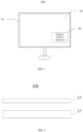
- FIG. 1 is a schematic structural diagram illustrating a display device 100 provided in implementations of the disclosure.
- the display device 100 of implementations of the disclosure may at least include a display module 10, a power-supply module 20, and a support frame 70.
- the display module 10 is fixed to the support frame 70.
- the power-supply module 20 is disposed on the back of the display module 10, that is, a non-display surface of the display module 10, that is, one side of the display module 10 facing away from a user.
- the display module 10 is configured to display an image.
- the power-supply module 20 is electrically coupled with the display module 10, and configured to provide a power-supply voltage for the display module 10 to display an image.
- the support frame 70 supports and protects the display module 10 and the power-supply module 20.
- the display module 10 further has a display surface opposite to the non-display surface, that is, a front surface of the display module 10, that is, one side of the display module 10 facing the user.
- the display surface facing the user who uses the display device 100 is configured to display an image.
- FIG. 2 is a schematic structural diagram illustrating a display module 10 of the display device 100 illustrated in FIG. 1 .
- the display module 10 of implementations of the disclosure may at least include a display panel 13 and a Backlight Module (BM) 17.
- the display panel 13 is disposed on a light-emitting side of the BM 17.
- the BM 17 is configured to provide the display panel 13 with lights for display.
- the display panel 13 is configured to display an image by emitting lights according to image data to-be-displayed.
- the display panel of implementations of the disclosure may be a display panel that adopts a Passive Matrix (PM) drive mode, such as a Micro Light-Emitting Diode (Micro-LED) display panel, an Organic Light-Emitting Diode (OLED) display panel, a Mini Light-Emitting Diode (Mini-LED) display panel, or the like.
- PM Passive Matrix
- the display module 10 further includes other elements or components, for example, a signal processor, a signal sensing module, etc.
- FIG. 3 is a schematic functional structural diagram illustrating a drive circuit 11 provided in implementations of the disclosure.
- the display module 10 of implementation of the disclosure at least includes a drive circuit 11.
- the drive circuit 11 may be disposed in a peripheral area of the display panel 13.
- the drive circuit 11 is electrically coupled with the display panel 13, and configured to provide a drive signal for the display panel 13.
- the drive circuit 11 is electrically coupled with the BM 17, and cooperates with the BM 17 to make the display panel 13 display an image.
- the drive circuit 11 of implementations of the disclosure can be applied to the display panel 13.
- the drive circuit 11 at least includes at least one display control module 30, a display drive module 40, and a discharge control module 50.
- the display control module 30 is electrically coupled with the display drive module 40.
- the display control module 30 is configured to receive a data signal Data, and selectively transmit a first power-supply voltage Vdd to the display drive module 40 according to the data signal Data.
- the display drive module 40 is configured to receive a scan signal Scan and the data signal Data.
- a light-emitting element 41 is driven by the first power-supply voltage Vdd to emit lights under control of the scan signal Scan and the data signal Data.
- the discharge control module 50 is electrically coupled with the display drive module 40.
- the discharge control module 50 is configured to receive the first power-supply voltage Vdd, receive the scan signal Scan from the display drive module 40, and discharge the display panel 13 by adjusting a potential of the scan signal Scan when the first power-supply voltage Vdd drops (e.g., when the display module 10 is to be powered off).
- transmission of the first power-supply voltage Vdd in the display drive module 40 can be selectively controlled, that is, timing adjustment of the first power-supply voltage is achieved, which can effectively ensure accurate transmission of the first power-supply voltage Vdd, and avoid screen flickering caused by abnormal light emission of the display drive module 40 when powered on and powered off.
- the display drive module 40 may be a 2T1C pixel circuit. In other implementations, the display drive module 40 may also be a 3T1C pixel circuit, a 4T1C pixel circuit, a 7T2C pixel circuit, etc., which is not limited in the disclosure.
- FIG. 4 is a circuit structural diagram of the drive circuit 11 illustrated in FIG. 3 .
- the display control module 30 of implementations of the disclosure is configured to adjust a power-on timing of the first power-supply voltage Vdd.
- the display control module 30 includes a first data-signal end a, a power input end b, and a signal output end c.
- the display control module 30 is configured to receive the data signal Data from the first data-signal end a, and receive the first power-supply voltage Vdd from the power input end b.
- the display control module 30 is configured to selectively control, according to the data signal Data, outputting of the first power-supply voltage Vdd to the display drive module 40 from the signal output end c.
- the display control module 30 further includes a first comparator 31, a first transistor 33, and a first threshold unit (not illustrated).
- the first comparator 31 includes a non-inverting input end, an inverting input end, and an output end.
- the data signal Data is inputted to the first comparator 31 via the non-inverting input end.
- the first threshold unit is configured to output a first threshold voltage Vf1, where the first threshold voltage Vf1 is inputted to the first comparator 31 via the inverting input end.
- the first comparator 31 is configured to compare a voltage of the data signal Data with the first threshold voltage Vf1, and output a level signal at its output end according to a comparison result, where the level signal indicates whether the data signal Data corresponds to a working value.
- the output end of the first comparator 31 is configured to output the level signal of a first potential, where the level signal of a first potential indicates that the data signal Data corresponds to a working value. Conversely, if the voltage of the data signal Data is lower than or equal to the first threshold voltage Vf1, the output end of the first comparator 31 is configured to output the level signal of a second potential, where the level signal of a second potential indicates that the data signal Data corresponds to a non-working value.
- a set value of the first threshold voltage Vf1 is smaller than the working value of the data signal Data, so that the data signal Data can be correctly transmitted in the display drive module 40.
- the first comparator 31 may be a voltage comparator.
- the first potential may be a high potential, and accordingly, the level signal of the first potential may be a level signal of a high potential.
- the second potential may be a low potential, and accordingly, the level signal of the second potential may be a level signal of a low potential, which is not limited in the disclosure.
- the first transistor 33 is configured to selectively transmit the first power-supply voltage Vdd to the display drive module 40 according to the level signal.
- the first transistor 33 includes a control end, a first end, and a second end.
- the control end of the first transistor 33 is electrically coupled with the output end of the first comparator 31 to receive the level signal, where the first transistor 33 is in an on-state or an off-state under control of the level signal.
- the first end of the first transistor 33 is electrically coupled with the power input end b, to receive the first power-supply voltage Vdd from the power input end b.
- the second end of the first transistor 33 is electrically coupled with the signal output end c. The first end and the second end of the first transistor 33 are selectively connected or disconnected according to the level signal.
- the control end of the first transistor 33 receives the level signal of a first potential from the output end of the first comparator 31, the first end and the second end of the first transistor 33 are electrically connected, that is, the first transistor 33 is in an on-state. In this situation, the first power-supply voltage Vdd is transmitted to the display drive module 40 from the signal output end c, to drive the light-emitting element 41 to emit lights. If the control end of the first transistor 33 receives the level signal of a second potential from the output end of the first comparator 31, the first end and the second end of the first transistor 33 are electrically disconnected, that is, the first transistor 33 is in an off-state. In this situation, the first power-supply voltage Vdd cannot be transmitted to the signal output end c, and accordingly, the first power-supply voltage Vdd cannot be transmitted to the display drive module 40.
- the first transistor 33 may be a Metal-Oxide-Semiconductor Field-Effect Transistor (MOSFET), which is not limited in the disclosure.
- MOSFET Metal-Oxide-Semiconductor Field-Effect Transistor
- the display control module 30 by arranging the display control module 30, whether the data signal Data corresponds to a working value can be determined according to the potential of the level signal outputted by the output end of the first comparator 31, so that the power-supply voltage Vdd is selectively supplied to the display drive module 40.
- the display drive module 40 is controlled to emit lights only when the display drive module 40 receives the first power-supply voltage Vdd, which can avoid abnormal light emission of the display drive module 40 caused by a wrong power-on timing of the first power-supply voltage Vdd, thereby improving a display effect of the display panel.
- the display drive module 40 includes a first scan-signal end d, a second data-signal end e, and a first power receiving end f.
- the display drive module 40 is configured to receive the scan signal Scan from the first scan-signal end d, and the display drive module 40 is configured to receive the data signal Data from the second data-signal end e.
- the first power receiving end f is electrically coupled with the signal output end c to receive the first power-supply voltage Vdd, that is, the display drive module 40 is electrically coupled with the second end of the first transistor 33 of the display control module 30 through the first power receiving end f and the signal output end c.
- the display drive module 40 includes the light-emitting element 41, a second transistor 42, and a third transistor 43.
- the second transistor 42 and the third transistor 43 each include a control end, a first end, and a second end.
- the control end of the second transistor 42 is electrically coupled with the first scan-signal end d to receive the scan signal Scan.
- the second transistor 42 is in an on-state or an off-state under control of the scan signal Scan, that is, the first end and the second end of the second transistor 42 are controlled to be electrically connected or disconnected.
- the first end of the second transistor 42 is electrically coupled with the second data-signal end e to receive the data signal Data.
- the second end of the second transistor 42 is electrically coupled with the control end of the third transistor 43.
- the second transistor 42 is configured to selectively transmit the data signal Data to the control end of the third transistor 43 according to the scan signal Scan.
- the first end of the third transistor 43 is electrically coupled with the first power receiving end f to receive the first power-supply voltage Vdd from the first power receiving end f, that is, the first end of the third transistor 43 is electrically coupled with the second end of the first transistor 33 to receive the first power-supply voltage Vdd.
- the second end of the third transistor 43 is electrically coupled with the light-emitting element 41.
- the control end of the third transistor 43 is configured to receive the data signal Data transmitted by the second transistor 42.
- the second end and the third end of the third transistor 43 are electrically connected or disconnected according to the data signal Data, to selectively transmit the first power-supply voltage Vdd to the light-emitting element 41 from the first power receiving end f.
- the control end of the second transistor 42 when the control end of the second transistor 42 receives the scan signal Scan of a first potential, the second transistor 42 is in an on-state, to transmit the data signal Data to the control end of the third transistor 43. If the control end of the third transistor 43 receives the data signal Data of a first potential, the first end and the second end of the third transistor 43 are electrically connected, that is, the third transistor 43 is in an on-state, to transmit the first power-supply voltage Vdd to the light-emitting element 41 from the first power receiving end f.
- the control end of the third transistor 43 receives the data signal Data of a second potential, the first end and the second end of the third transistor 43 are electrically disconnected, that is, the third transistor 43 is in an off-state, and thus, the first power-supply voltage Vdd cannot be transmitted to the light-emitting element 41.
- the control end of the second transistor 42 When the control end of the second transistor 42 receives the scan signal Scan of a second potential, the second transistor 42 is in an off-state, and thus, the data signal Data cannot be transmitted to the control end of the third transistor 43.
- the first power-supply voltage Vdd is transmitted to the light-emitting element 41 from the first power receiving end f, to drive the light-emitting element 41 to emit lights.
- the light-emitting element 41 has a positive pole (also called “anode”) and a negative pole (also called “cathode”).
- the positive pole of the light-emitting element 41 is electrically coupled with the second end of the third transistor 43
- the negative pole of the light-emitting element 41 is electrically coupled with a reference ground GND.
- the light-emitting element 41 receives the first power-supply voltage Vdd from the second end of the third transistor 43
- the light-emitting element 41 emits lights.
- no first power-supply voltage Vdd is received by the light-emitting element 41 from the second end of the third transistor 43, the light-emitting element 41 does not emit lights.
- the display drive module 40 further includes a bypass capacitor 45.
- a first end of the bypass capacitor 45 is electrically coupled with the control end of the third transistor 43, and a second end of the bypass capacitor 45 is electrically coupled with the reference ground GND to protect the light-emitting element 41 from being damaged.
- the second transistor 42, the third transistor 43, and the bypass capacitor 45 of the display drive module 40 each may be disposed in the display panel 13.
- the second transistor 42 and the third transistor 43 each may be a Thin Film Transistor (TFT), which is not limited in the disclosure.
- TFT Thin Film Transistor
- the discharge control module 50 includes a second power receiving end g, a second scan-signal end h, and a discharge end i.
- the discharge control module 50 is configured to transmit the residual first power-supply voltage Vdd to the reference ground GND for release, that is, the display device 100 is discharged through the scan signal Scan.
- the discharge control module 50 is configured to receive the first power-supply voltage Vdd through the second power receiving end g, and the discharge control module 50 is configured to selectively pull up the scan signal Scan to the first potential (e.g., a high level VGH of the scan signal Scan illustrated in FIG.
- the display device 100 is discharged through the scan signal Scan.
- the first potential e.g., a high level VGH of the scan signal Scan.
- the TFTs are all on, and thus, residual charges of the whole display panel can be released faster.
- the discharge control module 50 is configured to determine whether the display device 100 (e.g., the display module 10) is to be powered off or restarted according to a potential change of the first power-supply voltage Vdd.
- the discharge control module 50 further includes a flip-flop 51, a second comparator 53, a resistor 55, a fourth transistor 56, and a second threshold unit (not illustrated).
- the flip-flop 51 includes a preset end D, a clear end R, and a latch output end Q.
- the first power-supply voltage Vdd is inputted to the flip-flop 51 via the clear end R, that is, the clear end R is electrically coupled with the second power receiving end g to receive the first power-supply voltage Vdd.
- One end of the resistor 55 is electrically coupled with the preset end D, and the other end of the resistor 55 is configured to receive a second power-supply voltage VIN, that is, the second power-supply voltage VIN is transmitted to the preset end D via the resistor 55.
- the latch output end Q is electrically coupled with the second comparator 53.
- the flip-flop 51 is configured to output a trigger signal of a first potential at the latch output end Q upon detecting that the received first power-supply voltage Vdd drops.
- the second power-supply voltage VIN is a total input voltage of the whole light-emitting element 41.
- the flip-flop 51 may be a falling edge triggered D flip-flop
- the resistor 55 may be a trigger resistor, which are not limited in the disclosure.
- the second comparator 53 includes a non-inverting input end, an inverting input end, and an output end.
- the non-inverting input end of the second comparator 53 is electrically coupled with the latch output end Q of the flip-flop 51 to receive the trigger signal of a first potential.
- the inverting input end of the second comparator 53 is configured to receive a second threshold voltage Vf2 provided by the second threshold unit.
- the output end of the second comparator 53 is electrically coupled with the fourth transistor 56.
- the second comparator 53 is configured to compare the trigger signal of a first potential with the second threshold voltage Vf2, and output a discharge control signal from the output end of the second comparator 53 to the fourth transistor 56 according to a comparison result.
- the discharge control signal indicates whether residual charges of the display module 10 need to be released at this time.
- the output end of the second comparator 53 is configured to output the discharge control signal of a first potential, where the discharge control signal of a first potential indicates that the first power-supply voltage Vdd needs to be released. Conversely, if the voltage of the trigger signal of the first potential is lower than or equal to the second threshold voltage Vf2, the output end of the second comparator 53 is configured to output the discharge control signal of a second potential, where the discharge control signal of a second potential indicates that the first power-supply voltage Vdd does not need to be released.
- the trigger signal may be a high-level signal.
- the second comparator 53 may be a voltage comparator.
- the fourth transistor 56 includes a control end, a first end, and a second end.
- the control end of the fourth transistor 56 is electrically coupled with the output end of the second comparator 53 to receive the discharge control signal from the output end of the second comparator 53, where the fourth transistor 56 is in an on-state or an off-state under control of the discharge control signal.
- the first end of the fourth transistor 56 is electrically coupled with the second scan-signal end h, to transmit the scan signal Scan through the second scan-signal end h.
- the second end of the fourth transistor 56 is electrically coupled with the discharge end i to receive the scan signal Scan of a first potential (e.g., a scan signal Scan of a high level VGH) from the discharge end i.
- the fourth transistor 56 is configured to selectively pull up the scan signal Scan under control of the discharge control signal, for example, make the scan signal Scan have a high level VGH.
- the control end of the fourth transistor 56 receives the discharge control signal of a first potential
- the first end and the second end of the fourth transistor 56 are electrically connected, that is, the fourth transistor 56 is in an on-state
- the second end of the fourth transistor 56 receives the scan signal Scan of a first potential (e.g., a scan signal of a high level VGH) from the discharge end i, so that the scan signal Scan at the second scan-signal end h can be pulled up to have the first potential.
- a first potential e.g., a scan signal of a high level VGH
- the display panel 13 can be discharged by pulling up the scan signal Scan.
- the control end of the fourth transistor 56 When the control end of the fourth transistor 56 receives the discharge control signal of a second potential, the first end and the second end of the fourth transistor 56 are electrically disconnected, that is, the fourth transistor 56 is in an off-state, and the second end of the fourth transistor 56 cannot receive the scan signal Scan of a first potential from the discharge end i, so that the scan signal Scan at the second scan-signal end h cannot be pulled up to have the first potential.
- the second power-supply voltage VIN may be a total input voltage of the display device 100, which is not limited in the disclosure.
- the phrase "the first power-supply voltage Vdd needs to be released” may specifically refer to residual charges in the whole display module 10 when the display device 100 is to be powered off or restarted, or charges generated due to jitter of the first power-supply voltage Vdd, which is not limited in the disclosure.
- a potential change of the first power-supply voltage Vdd in the drive circuit 11 e.g., when the display module 10 executes a power-off or restart command, the first power-supply voltage Vdd drops
- the discharge control module 50 a potential change of the first power-supply voltage Vdd in the drive circuit 11 (e.g., when the display module 10 executes a power-off or restart command, the first power-supply voltage Vdd drops) can be detected in real time.
- the discharge control module 50 is configured to receive the scan signal Scan of a first potential (e.g., a scan signal of a high level VGH) from the discharge end i, so that the scan signal Scan at the second scan-signal end h can be pulled up to have the first potential (i.e., a high level VGH), that is, the display device 100 can be discharged through the scan signal Scan.
- a first potential e.g., a scan signal of a high level VGH
- the first potential i.e., a high level VGH
- the TFTs are all on, and thus, residual charges of the whole display panel 13 can be released faster, which can avoid screen flickering of the display panel 13 caused by the light-emitting element 41 being powered on by mistake due to remaining of the first power-supply voltage Vdd in the display module 10.
- FIG. 5 is a partial circuit diagram of a display module 10 provided in implementations of the disclosure.
- multiple scan lines S1-Sn extending along a first direction F1 and multiple data lines D1-Dm extending along a second direction F2 are arranged in the display panel 13 and cooperatively form a grid.
- the first direction F1 is perpendicular to the second direction F2.
- the multiple scan lines S1-Sn are insulated from one another, the multiple data lines D1-Dm are insulated from one another, and the multiple scan lines S1-Sn and the multiple data lines D1-Dm are insulated from one another.
- the multiple scan lines S 1-Sn are spaced apart from one another and insulated from one another
- the multiple data lines D1-Dm are spaced apart from one another and insulated from one another
- the multiple scan lines S 1-Sn and the multiple data lines D1-Dm are insulated from one another.
- Each of intersections of the multiple scan lines S1-Sn and the multiple data lines D1-Dm is provided with a display drive module 40.
- the display drive module 40 is disposed between any two adjacent scan lines and any two adjacent data lines. Display drive modules 40 in a same column are electrically coupled with a same data line, and display drive modules 40 in a same row are electrically coupled with a same scan line.
- multiple display drive modules 40 are arranged in an array.
- each of the scan lines is configured to receive a scan signal Scan.
- Each of the scan lines is electrically coupled with a discharge control module 50, to control the scan signal Scan in the scan line to have a first potential (e.g., to make the scan signal Scan have a high level VGH) when the display device 100 is to be powered off or restarted, so that the display panel 13 can be discharged through the scan signal Scan.
- a discharge control module 50 to control the scan signal Scan in the scan line to have a first potential (e.g., to make the scan signal Scan have a high level VGH) when the display device 100 is to be powered off or restarted, so that the display panel 13 can be discharged through the scan signal Scan.
- Each of the data lines is configured to receive a data signal Data.
- Each of the data lines is electrically coupled with a display control module 30.
- the display control module 30 is configured to selectively transmit a first power-supply voltage Vdd to the display drive module 40 according to the data signal Data.
- FIG. 6 is a schematic timing diagram of a drive circuit 11 provided in implementations of the disclosure.
- a horizontal axis represents time
- a vertical-axis value on the horizontal axis represents a voltage of 0 volts
- a vertical-axis value above the horizontal axis represents a positive potential
- a vertical-axis value below the horizontal axis represents a negative potential.
- the timing of a second power-supply voltage VIN illustrates powered-on time and powered-off time of the display device 100.
- the display device 100 is powered on at a time point A and powered off at a time point B. That is, the time point A is time when the display device 100 is powered on, and the time point B is time when the display device 100 is powered off.
- a voltage of the data signal Data becomes higher than a first threshold voltage Vf1, that is, when the voltage of the data signal Data corresponds to a working value, the first power-supply voltage Vdd is transmitted to the drive circuit 11.
- a first threshold voltage Vf1 that is, when the voltage of the data signal Data corresponds to a working value
- the first power-supply voltage Vdd is transmitted to the drive circuit 11.
- row-based scanning with the scan signal Scan is performed, and the scan signal Scan is periodically switched between a first potential and a second potential.
- the display device 100 is to be powered off or restarted, that is, the first power-supply voltage Vdd gradually decreases, and thus, the display panel 13 is discharged by the discharge control module 50 through the scan signal Scan, until the first power-supply voltage Vdd drops to 0 volts. Since all TFTs of the drive circuit 11 are discharged from the first potential (e.g., a high level VGH of the scan signal Scan), the TFTs are all on, so that the scan signal Scan can be transmitted to a reference ground GND and released quickly. As such, residual charges of the whole display panel can be released more quickly, which can effectively avoid screen flickering of the display device 100.
- the first potential e.g., a high level VGH of the scan signal Scan
- the disclosure further provides a display module 10.
- the display module 10 includes the drive circuit 11 and the display panel 13 illustrated in FIG. 3 and FIG. 4 .
- the drive circuit 11 is electrically coupled with the display panel 13, and configured to drive the display panel 13 to display different images.
- the disclosure further provides a display device 100.
- the display device 100 includes the above display module 10 and a power-supply module 20.
- the power-supply module 20 is disposed on a non-display surface of the display module 10, and configured to provide a power-supply voltage for the display module 10 to display images.
- the display device 100 of implementations of the disclosure may be any product or component with a display function, such as a notebook-computer display screen, a Liquid Crystal Display (LCD), an LCD TV, a mobile phone, a tablet computer, etc.
- a display function such as a notebook-computer display screen, a Liquid Crystal Display (LCD), an LCD TV, a mobile phone, a tablet computer, etc.
- the display device 100 further includes other necessary components and components such as a high-voltage board and a keyboard.
- Those skilled in the art can make supplements according to a specific type and an actual function of the display device 100, which will not be repeated herein.
- the display device 100 can also be applied to an electronic device with functions such as Personal Digital Assistant (PDA) and/or a music player, where the electronic device may include a mobile phone, a tablet computer, and a wearable electronic device with a wireless communication function (e.g., a smart watch), etc.
- PDA Personal Digital Assistant
- the above electronic device may also be other electronic devices, such as a laptop computer having a touch-sensitive surface (e.g., a touch panel).
- the display module 10, and the display device 100 of the disclosure by providing the display control module 30 and the discharge control module 50 in the drive circuit 11, transmission of the first power-supply voltage Vdd in the display drive module 40 can be selectively controlled, that is, timing adjustment of the first power-supply voltage Vdd is achieved, which can effectively ensure accurate transmission of the first power-supply voltage, and avoid screen flickering caused by abnormal light emission of the display drive module 40 when powered on and powered off, thereby improving a display effect of the display panel 13.
- the discharge control module 50 in the drive circuit 11 a potential of the first power-supply voltage Vdd in the drive circuit 11 can be detected in real time.
- the discharge control module 50 When the first power-supply voltage Vdd drops, that is, when the display device 100 is to be powered off or restarted (e.g., when the display device 100 is about to be powered off), discharging of the display device 100 is implemented with the discharge control module 50 through the scan signal Scan, so that all TFTs are discharged from the first potential (e.g., a high level VGH of the scan signal Scan) when the display device 100 is to be powered off.
- the first potential e.g., a high level VGH of the scan signal Scan
- the TFTs are all on, and thus, residual charges of the whole display panel can be released faster, which can avoid screen flickering of the display panel 13 caused by the display drive module 40 being powered on by mistake due to jitter of the first power-supply voltage Vdd or residual charges of the whole display module 10 in the drive circuit 11. Therefore, a display effect of the display module 10 and the display device 100 can be improved effectively, and a user experience can also be improved.
- an implementation means that particular features, structures, materials, or properties described in conjunction with the implementations or examples may be defined in at least one implementation or example of the disclosure.
- schematic representations of the above terms do not necessarily refer to a same implementation or example.
- the particular features, structures, materials, or properties described may be combined in any suitable manner in any one or more implementations or examples.
Landscapes
- Engineering & Computer Science (AREA)
- Physics & Mathematics (AREA)
- Computer Hardware Design (AREA)
- General Physics & Mathematics (AREA)
- Theoretical Computer Science (AREA)
- Control Of Indicators Other Than Cathode Ray Tubes (AREA)
- Control Of El Displays (AREA)
Abstract
Description
- This application claims priority to
Chinese Application Patent Serial No. 202210759722.X, entitled "DRIVE CIRCUIT, DISPLAY MODULE, AND DISPLAY DEVICE", and filed June 30, 2022 - This application relates to the field of display technologies, and particularly to a drive circuit, a display module having the drive circuit, and a display device having the display module.
- Organic Light-Emitting Diode (OLED) displays have many advantages such as fast response speed, high contrast, low power consumption, easy to match a system integrated circuit to drive, light and thin structure, easy to realize flexible display, etc., and therefore have been widely used in mobile phones, notebooks, and other display devices.
- The OLED display generally adopts Thin Film Transistors (TFT), however, a threshold voltage of a TFT decreases when a temperature of the OLED display increases, which may cause screen flickering when powered on after long-term high-temperature operation. Moreover, when the OLED display is powered on and powered off frequently, screen flickering when powered off may occur due to jitter of a power-supply voltage or residual charges in the OLED display.
- The disclosure provides a drive circuit, a display module, and a display device. A display control module and a discharge control module are provided in the drive circuit to adjust transmission timing of a first power-supply voltage, which can effectively ensure accurate transmission of the first power-supply voltage, and avoid screen flickering caused by abnormal light emission of a display drive module when powered on and powered off.
- In order to solve technical problems of the disclosure, the disclosure provides the following technical solutions.
- The disclosure provides a drive circuit. The drive circuit includes a display drive module configured to receive a scan signal and a data signal. The drive circuit further includes at least one display control module and a discharge control module. The display control module is electrically coupled with the display drive module. The display control module is configured to receive the data signal, and selectively transmit a first power-supply voltage to the display drive module according to the data signal. The display drive module is configured to transmit, under control of the scan signal and the data signal, the first power-supply voltage to a light-emitting element of the display drive module upon reception of the first power-supply voltage, to drive the light-emitting element to emit lights. The discharge control module is electrically coupled with the display drive module. The discharge control module is configured to receive the first power-supply voltage, and discharge the light-emitting element by adjusting a potential of the scan signal when the first power-supply voltage drops.
- In a second aspect, the disclosure further provides a display module. The display module includes a display panel and the above drive circuit. The drive circuit is electrically coupled with the display panel, and configured to drive the display panel to display different images.
- In a third aspect, the disclosure further provides a display device. The display device includes a power-supply module and the above display module. The power-supply module is disposed on a non-display surface of the display module, and configured to provide a power-supply voltage for the display module to display images.
- According to the drive circuit, the display module, and the display device of the disclosure, the display control module and the discharge control module are provided in the drive circuit to selectively control transmission of the first power-supply voltage in the display drive module, that is, timing adjustment of the first power-supply voltage is achieved, which can effectively ensure accurate transmission of the first power-supply voltage, and avoid screen flickering caused by abnormal light emission of the display drive module when powered on and powered off, thereby improving a display effect of the display module.
- In addition, by arranging the discharge control module in the drive circuit, a potential of the first power-supply voltage in the drive circuit can be detected in real time. When the first power-supply voltage drops, that is, when the display device is to be powered off or restarted, the display device is discharged by the discharge control module through the scan signal, so that all light-emitting elements are discharged from the first potential when the display device is to be powered off. As such, the light-emitting elements are all on, and residual charges of the whole display panel can be released faster, which can avoid screen flickering of the display panel caused by the display drive module being powered on by mistake due to jitter of the first power-supply voltage or residual charges of the whole display module in the drive circuit. Therefore, a display effect of the display module and the display device can be improved effectively, and a user experience can also be improved.
- In order to describe technical solutions of implementations of the disclosure or the related art more clearly, the following will give a brief description of accompanying drawings used for describing the implementations or the related art. Apparently, accompanying drawings described below are merely some implementations. Those of ordinary skill in the art can also obtain other accompanying drawings based on the accompanying drawings described below without creative efforts.
-
FIG. 1 is a schematic structural diagram illustrating a display device provided in implementations of the disclosure. -
FIG. 2 is a schematic structural diagram illustrating a display module of the display device illustrated inFIG. 1 . -
FIG. 3 is a schematic functional structural diagram illustrating a drive circuit provided in implementations of the disclosure. -
FIG. 4 is a circuit structural diagram of the drive circuit illustrated inFIG. 3 . -
FIG. 5 is a partial circuit diagram of a display module provided in implementations of the disclosure. -
FIG. 6 is a schematic timing diagram of a drive circuit provided in implementations of the disclosure. - In order to facilitate understanding of the disclosure, the disclosure will be described fully below with reference to accompanying drawings. The accompanying drawings illustrate exemplary implementations of the disclosure. However, the disclosure may be implemented in many different forms and is not limited to the implementations described herein. Rather, these implementations are provided to achieve a thorough and complete understanding of disclosed contents of the disclosure.
- The description of the following implementations refers to the accompanying drawings to illustrate practical exemplary implementations of the disclosure. In the context, reference signs of components, such as "first" and "second", are merely used to distinguish described objects rather than to describe a particular order or technical meaning. The terms "connection", "coupling", and the like in the disclosure, unless otherwise specified, include direct connection (coupling) and indirect connection (coupling). Directional terms in the disclosure, such as "upper", "lower", "front", "rear", "left", "right", "inner", "outer", "side", refer to directions of the accompanying drawings, and therefore, the directional terms herein are merely for better and clearer description and understanding of the disclosure, rather than indicating or implying that a device or an element referred to must have a specific orientation, and be constructed and operated in a specific orientation, which should not be construed as limiting the disclosure.
- It should be noted that, in the description of the disclosure, unless the context clearly indicates otherwise, the terms "mounted", "coupled", "connected", and variations thereof should be broadly understood. For example, the terms may refer to a fixed connection, a removable connection, or an integrated connection; or, may refer to a mechanical connection; or, may refer to a direct connection, an indirect connection via an intermediary, or an internal communication or interaction of two elements. For those skilled in the art, the meanings of the above terms referred to in the disclosure may be understood based on specific situations. It should be noted that, the terms "first", "second", and the like used in the specification, the claims, and the accompany drawings of the disclosure are used to distinguish different objects rather than to describe a particular order. In addition, the terms "include", "comprise", "have", and variations thereof are intended to cover non-exclusive inclusion. For example, a process, method, system, product, or device including a series of steps or units is not limited to the listed steps or units, on the contrary, it can optionally include other steps or units that are not listed; alternatively, other steps or units inherent to the process, method, product, or device can be included either. In addition, the terms "include/comprise", "may include/comprise", "contain", and "may contain" indicate presence of a disclosed function, operation, element, etc., and may indicate, but not limited to, one or more other more functions, operations, elements, etc. Furthermore, the terms "include/comprise" or "contain" indicate presence of a corresponding feature, number, step, operation, element, component, or combinations thereof disclosed in the specification, but do not preclude presence or addition of one or more other features, numbers, steps, operations, elements, components, or combinations thereof, and these terms are intended to cover non-exclusive inclusion. It should also be understood that, the term "at least one" herein means one and more, such as one, two, or three, or the like. The term "a plurality of/multiple" herein means at least two, such as two or three, or the like, unless otherwise specifically defined. The terms "
step 1", "step 2", and the like in the specification, the claims, and the accompany drawings of the disclosure are used to distinguish different objects rather than to describe a particular order. - In the field of display technologies, a display device generally includes a display panel and a backlight component, where the display panel is mounted on a light-emitting side of the backlight component, and the backlight component is configured to provide backlight for the display panel to adjust the display panel to display different images.
- Referring to
FIG. 1, FIG. 1 is a schematic structural diagram illustrating adisplay device 100 provided in implementations of the disclosure. As illustrated inFIG. 1 , thedisplay device 100 of implementations of the disclosure may at least include adisplay module 10, a power-supply module 20, and asupport frame 70. Thedisplay module 10 is fixed to thesupport frame 70. The power-supply module 20 is disposed on the back of thedisplay module 10, that is, a non-display surface of thedisplay module 10, that is, one side of thedisplay module 10 facing away from a user. Thedisplay module 10 is configured to display an image. The power-supply module 20 is electrically coupled with thedisplay module 10, and configured to provide a power-supply voltage for thedisplay module 10 to display an image. Thesupport frame 70 supports and protects thedisplay module 10 and the power-supply module 20. - It can be understood that, the
display module 10 further has a display surface opposite to the non-display surface, that is, a front surface of thedisplay module 10, that is, one side of thedisplay module 10 facing the user. The display surface facing the user who uses thedisplay device 100 is configured to display an image. - Referring to
FIG. 2 together,FIG. 2 is a schematic structural diagram illustrating adisplay module 10 of thedisplay device 100 illustrated inFIG. 1 . Thedisplay module 10 of implementations of the disclosure may at least include adisplay panel 13 and a Backlight Module (BM) 17. Thedisplay panel 13 is disposed on a light-emitting side of theBM 17. TheBM 17 is configured to provide thedisplay panel 13 with lights for display. Thedisplay panel 13 is configured to display an image by emitting lights according to image data to-be-displayed. The display panel of implementations of the disclosure may be a display panel that adopts a Passive Matrix (PM) drive mode, such as a Micro Light-Emitting Diode (Micro-LED) display panel, an Organic Light-Emitting Diode (OLED) display panel, a Mini Light-Emitting Diode (Mini-LED) display panel, or the like. - In exemplary implementations of the disclosure, the
display module 10 further includes other elements or components, for example, a signal processor, a signal sensing module, etc. - Referring to
FIG. 3 together,FIG. 3 is a schematic functional structural diagram illustrating adrive circuit 11 provided in implementations of the disclosure. Further, thedisplay module 10 of implementation of the disclosure at least includes adrive circuit 11. Thedrive circuit 11 may be disposed in a peripheral area of thedisplay panel 13. Thedrive circuit 11 is electrically coupled with thedisplay panel 13, and configured to provide a drive signal for thedisplay panel 13. Thedrive circuit 11 is electrically coupled with theBM 17, and cooperates with theBM 17 to make thedisplay panel 13 display an image. - The
drive circuit 11 of implementations of the disclosure can be applied to thedisplay panel 13. Thedrive circuit 11 at least includes at least onedisplay control module 30, adisplay drive module 40, and adischarge control module 50. Thedisplay control module 30 is electrically coupled with thedisplay drive module 40. Thedisplay control module 30 is configured to receive a data signal Data, and selectively transmit a first power-supply voltage Vdd to thedisplay drive module 40 according to the data signal Data. Thedisplay drive module 40 is configured to receive a scan signal Scan and the data signal Data. When the display drive module receives the first power-supply voltage, a light-emittingelement 41 is driven by the first power-supply voltage Vdd to emit lights under control of the scan signal Scan and the data signal Data. Thedischarge control module 50 is electrically coupled with thedisplay drive module 40. Thedischarge control module 50 is configured to receive the first power-supply voltage Vdd, receive the scan signal Scan from thedisplay drive module 40, and discharge thedisplay panel 13 by adjusting a potential of the scan signal Scan when the first power-supply voltage Vdd drops (e.g., when thedisplay module 10 is to be powered off). - In implementations of the disclosure, by arranging the
display control module 30 and thedischarge control module 50 in thedrive circuit 11, transmission of the first power-supply voltage Vdd in thedisplay drive module 40 can be selectively controlled, that is, timing adjustment of the first power-supply voltage is achieved, which can effectively ensure accurate transmission of the first power-supply voltage Vdd, and avoid screen flickering caused by abnormal light emission of thedisplay drive module 40 when powered on and powered off. - In implementations of the disclosure, the
display drive module 40 may be a 2T1C pixel circuit. In other implementations, thedisplay drive module 40 may also be a 3T1C pixel circuit, a 4T1C pixel circuit, a 7T2C pixel circuit, etc., which is not limited in the disclosure. - Referring to
FIG. 4 together,FIG. 4 is a circuit structural diagram of thedrive circuit 11 illustrated inFIG. 3 . Thedisplay control module 30 of implementations of the disclosure is configured to adjust a power-on timing of the first power-supply voltage Vdd. Thedisplay control module 30 includes a first data-signal end a, a power input end b, and a signal output end c. Thedisplay control module 30 is configured to receive the data signal Data from the first data-signal end a, and receive the first power-supply voltage Vdd from the power input end b. Thedisplay control module 30 is configured to selectively control, according to the data signal Data, outputting of the first power-supply voltage Vdd to thedisplay drive module 40 from the signal output end c. - In specific implementations of the disclosure, the
display control module 30 further includes afirst comparator 31, afirst transistor 33, and a first threshold unit (not illustrated). Thefirst comparator 31 includes a non-inverting input end, an inverting input end, and an output end. The data signal Data is inputted to thefirst comparator 31 via the non-inverting input end. The first threshold unit is configured to output a first threshold voltage Vf1, where the first threshold voltage Vf1 is inputted to thefirst comparator 31 via the inverting input end. Thefirst comparator 31 is configured to compare a voltage of the data signal Data with the first threshold voltage Vf1, and output a level signal at its output end according to a comparison result, where the level signal indicates whether the data signal Data corresponds to a working value. - Specifically, if the voltage of the data signal Data is higher than the first threshold voltage Vf1, the output end of the
first comparator 31 is configured to output the level signal of a first potential, where the level signal of a first potential indicates that the data signal Data corresponds to a working value. Conversely, if the voltage of the data signal Data is lower than or equal to the first threshold voltage Vf1, the output end of thefirst comparator 31 is configured to output the level signal of a second potential, where the level signal of a second potential indicates that the data signal Data corresponds to a non-working value. - It can be understood that, a set value of the first threshold voltage Vf1 is smaller than the working value of the data signal Data, so that the data signal Data can be correctly transmitted in the
display drive module 40. - In implementations of the disclosure, the
first comparator 31 may be a voltage comparator. The first potential may be a high potential, and accordingly, the level signal of the first potential may be a level signal of a high potential. The second potential may be a low potential, and accordingly, the level signal of the second potential may be a level signal of a low potential, which is not limited in the disclosure. - In specific implementations of the disclosure, the
first transistor 33 is configured to selectively transmit the first power-supply voltage Vdd to thedisplay drive module 40 according to the level signal. Thefirst transistor 33 includes a control end, a first end, and a second end. The control end of thefirst transistor 33 is electrically coupled with the output end of thefirst comparator 31 to receive the level signal, where thefirst transistor 33 is in an on-state or an off-state under control of the level signal. The first end of thefirst transistor 33 is electrically coupled with the power input end b, to receive the first power-supply voltage Vdd from the power input end b. The second end of thefirst transistor 33 is electrically coupled with the signal output end c. The first end and the second end of thefirst transistor 33 are selectively connected or disconnected according to the level signal. - Specifically, if the control end of the
first transistor 33 receives the level signal of a first potential from the output end of thefirst comparator 31, the first end and the second end of thefirst transistor 33 are electrically connected, that is, thefirst transistor 33 is in an on-state. In this situation, the first power-supply voltage Vdd is transmitted to thedisplay drive module 40 from the signal output end c, to drive the light-emittingelement 41 to emit lights. If the control end of thefirst transistor 33 receives the level signal of a second potential from the output end of thefirst comparator 31, the first end and the second end of thefirst transistor 33 are electrically disconnected, that is, thefirst transistor 33 is in an off-state. In this situation, the first power-supply voltage Vdd cannot be transmitted to the signal output end c, and accordingly, the first power-supply voltage Vdd cannot be transmitted to thedisplay drive module 40. - In specific implementations of the disclosure, the
first transistor 33 may be a Metal-Oxide-Semiconductor Field-Effect Transistor (MOSFET), which is not limited in the disclosure. - In implementations of the disclosure, by arranging the
display control module 30, whether the data signal Data corresponds to a working value can be determined according to the potential of the level signal outputted by the output end of thefirst comparator 31, so that the power-supply voltage Vdd is selectively supplied to thedisplay drive module 40. As such, thedisplay drive module 40 is controlled to emit lights only when thedisplay drive module 40 receives the first power-supply voltage Vdd, which can avoid abnormal light emission of thedisplay drive module 40 caused by a wrong power-on timing of the first power-supply voltage Vdd, thereby improving a display effect of the display panel. - In implementations of the disclosure, as illustrated in
FIG. 4 , thedisplay drive module 40 includes a first scan-signal end d, a second data-signal end e, and a first power receiving end f. Thedisplay drive module 40 is configured to receive the scan signal Scan from the first scan-signal end d, and thedisplay drive module 40 is configured to receive the data signal Data from the second data-signal end e. The first power receiving end f is electrically coupled with the signal output end c to receive the first power-supply voltage Vdd, that is, thedisplay drive module 40 is electrically coupled with the second end of thefirst transistor 33 of thedisplay control module 30 through the first power receiving end f and the signal output end c. - In specific implementations of the disclosure, the
display drive module 40 includes the light-emittingelement 41, asecond transistor 42, and athird transistor 43. Thesecond transistor 42 and thethird transistor 43 each include a control end, a first end, and a second end. The control end of thesecond transistor 42 is electrically coupled with the first scan-signal end d to receive the scan signal Scan. Thesecond transistor 42 is in an on-state or an off-state under control of the scan signal Scan, that is, the first end and the second end of thesecond transistor 42 are controlled to be electrically connected or disconnected. The first end of thesecond transistor 42 is electrically coupled with the second data-signal end e to receive the data signal Data. The second end of thesecond transistor 42 is electrically coupled with the control end of thethird transistor 43. Thesecond transistor 42 is configured to selectively transmit the data signal Data to the control end of thethird transistor 43 according to the scan signal Scan. - The first end of the
third transistor 43 is electrically coupled with the first power receiving end f to receive the first power-supply voltage Vdd from the first power receiving end f, that is, the first end of thethird transistor 43 is electrically coupled with the second end of thefirst transistor 33 to receive the first power-supply voltage Vdd. The second end of thethird transistor 43 is electrically coupled with the light-emittingelement 41. The control end of thethird transistor 43 is configured to receive the data signal Data transmitted by thesecond transistor 42. The second end and the third end of thethird transistor 43 are electrically connected or disconnected according to the data signal Data, to selectively transmit the first power-supply voltage Vdd to the light-emittingelement 41 from the first power receiving end f. - Specifically, when the control end of the
second transistor 42 receives the scan signal Scan of a first potential, thesecond transistor 42 is in an on-state, to transmit the data signal Data to the control end of thethird transistor 43. If the control end of thethird transistor 43 receives the data signal Data of a first potential, the first end and the second end of thethird transistor 43 are electrically connected, that is, thethird transistor 43 is in an on-state, to transmit the first power-supply voltage Vdd to the light-emittingelement 41 from the first power receiving end f. Conversely, if the control end of thethird transistor 43 receives the data signal Data of a second potential, the first end and the second end of thethird transistor 43 are electrically disconnected, that is, thethird transistor 43 is in an off-state, and thus, the first power-supply voltage Vdd cannot be transmitted to the light-emittingelement 41. - When the control end of the
second transistor 42 receives the scan signal Scan of a second potential, thesecond transistor 42 is in an off-state, and thus, the data signal Data cannot be transmitted to the control end of thethird transistor 43. - In other words, in these implementations, when the scan signal Scan has a first potential and the data signal Data has a first potential, the first power-supply voltage Vdd is transmitted to the light-emitting
element 41 from the first power receiving end f, to drive the light-emittingelement 41 to emit lights. - In specific implementations of the disclosure, the light-emitting
element 41 has a positive pole (also called "anode") and a negative pole (also called "cathode"). The positive pole of the light-emittingelement 41 is electrically coupled with the second end of thethird transistor 43, and the negative pole of the light-emittingelement 41 is electrically coupled with a reference ground GND. Specifically, when the light-emittingelement 41 receives the first power-supply voltage Vdd from the second end of thethird transistor 43, the light-emittingelement 41 emits lights. When no first power-supply voltage Vdd is received by the light-emittingelement 41 from the second end of thethird transistor 43, the light-emittingelement 41 does not emit lights. - In implementations of the disclosure, the
display drive module 40 further includes abypass capacitor 45. A first end of thebypass capacitor 45 is electrically coupled with the control end of thethird transistor 43, and a second end of thebypass capacitor 45 is electrically coupled with the reference ground GND to protect the light-emittingelement 41 from being damaged. - In specific implementations of the disclosure, the
second transistor 42, thethird transistor 43, and thebypass capacitor 45 of thedisplay drive module 40 each may be disposed in thedisplay panel 13. - In specific implementations of the disclosure, the
second transistor 42 and thethird transistor 43 each may be a Thin Film Transistor (TFT), which is not limited in the disclosure. - In implementations of the disclosure, as illustrated in
FIG. 4 , thedischarge control module 50 includes a second power receiving end g, a second scan-signal end h, and a discharge end i. When thedisplay device 100 is to be powered off or restarted, thedischarge control module 50 is configured to transmit the residual first power-supply voltage Vdd to the reference ground GND for release, that is, thedisplay device 100 is discharged through the scan signal Scan. Specifically, thedischarge control module 50 is configured to receive the first power-supply voltage Vdd through the second power receiving end g, and thedischarge control module 50 is configured to selectively pull up the scan signal Scan to the first potential (e.g., a high level VGH of the scan signal Scan illustrated inFIG. 4 ) according to the first power-supply voltage Vdd, so that the first power-supply voltage Vdd in thedisplay drive module 40 is transmitted to the reference ground GND for release, that is, thedisplay device 100 is discharged through the scan signal Scan. In this way, when thedisplay device 100 is to be powered off, all TFTs are discharged from the first potential (e.g., a high level VGH of the scan signal Scan). As such, the TFTs are all on, and thus, residual charges of the whole display panel can be released faster. - It can be understood that, when the
display device 100 executes a power-off or restart command, the first power-supply voltage Vdd drops. In these implementations, thedischarge control module 50 is configured to determine whether the display device 100 (e.g., the display module 10) is to be powered off or restarted according to a potential change of the first power-supply voltage Vdd. - In specific implementations of the disclosure, as illustrated in
FIG. 4 , thedischarge control module 50 further includes a flip-flop 51, a second comparator 53, aresistor 55, afourth transistor 56, and a second threshold unit (not illustrated). The flip-flop 51 includes a preset end D, a clear end R, and a latch output end Q. The first power-supply voltage Vdd is inputted to the flip-flop 51 via the clear end R, that is, the clear end R is electrically coupled with the second power receiving end g to receive the first power-supply voltage Vdd. One end of theresistor 55 is electrically coupled with the preset end D, and the other end of theresistor 55 is configured to receive a second power-supply voltage VIN, that is, the second power-supply voltage VIN is transmitted to the preset end D via theresistor 55. The latch output end Q is electrically coupled with the second comparator 53. The flip-flop 51 is configured to output a trigger signal of a first potential at the latch output end Q upon detecting that the received first power-supply voltage Vdd drops. In implementations of the disclosure, the second power-supply voltage VIN is a total input voltage of the whole light-emittingelement 41. - In specific implementations of the disclosure, the flip-
flop 51 may be a falling edge triggered D flip-flop, and theresistor 55 may be a trigger resistor, which are not limited in the disclosure. - In specific implementations of the disclosure, the second comparator 53 includes a non-inverting input end, an inverting input end, and an output end. The non-inverting input end of the second comparator 53 is electrically coupled with the latch output end Q of the flip-
flop 51 to receive the trigger signal of a first potential. The inverting input end of the second comparator 53 is configured to receive a second threshold voltage Vf2 provided by the second threshold unit. The output end of the second comparator 53 is electrically coupled with thefourth transistor 56. The second comparator 53 is configured to compare the trigger signal of a first potential with the second threshold voltage Vf2, and output a discharge control signal from the output end of the second comparator 53 to thefourth transistor 56 according to a comparison result. The discharge control signal indicates whether residual charges of thedisplay module 10 need to be released at this time. - Specifically, if a voltage of the trigger signal of the first potential is higher than the second threshold voltage Vf2, the output end of the second comparator 53 is configured to output the discharge control signal of a first potential, where the discharge control signal of a first potential indicates that the first power-supply voltage Vdd needs to be released. Conversely, if the voltage of the trigger signal of the first potential is lower than or equal to the second threshold voltage Vf2, the output end of the second comparator 53 is configured to output the discharge control signal of a second potential, where the discharge control signal of a second potential indicates that the first power-supply voltage Vdd does not need to be released. In implementations of the disclosure, the trigger signal may be a high-level signal.
- In implementations of the disclosure, the second comparator 53 may be a voltage comparator.
- In specific implementations of the disclosure, the
fourth transistor 56 includes a control end, a first end, and a second end. The control end of thefourth transistor 56 is electrically coupled with the output end of the second comparator 53 to receive the discharge control signal from the output end of the second comparator 53, where thefourth transistor 56 is in an on-state or an off-state under control of the discharge control signal. The first end of thefourth transistor 56 is electrically coupled with the second scan-signal end h, to transmit the scan signal Scan through the second scan-signal end h. The second end of thefourth transistor 56 is electrically coupled with the discharge end i to receive the scan signal Scan of a first potential (e.g., a scan signal Scan of a high level VGH) from the discharge end i. Thefourth transistor 56 is configured to selectively pull up the scan signal Scan under control of the discharge control signal, for example, make the scan signal Scan have a high level VGH. - Specifically, when the control end of the
fourth transistor 56 receives the discharge control signal of a first potential, the first end and the second end of thefourth transistor 56 are electrically connected, that is, thefourth transistor 56 is in an on-state, and the second end of thefourth transistor 56 receives the scan signal Scan of a first potential (e.g., a scan signal of a high level VGH) from the discharge end i, so that the scan signal Scan at the second scan-signal end h can be pulled up to have the first potential. As such, when the first power-supply voltage Vdd drops (e.g., when thedisplay module 10 is to be powered off or restarted), thedisplay panel 13 can be discharged by pulling up the scan signal Scan. - When the control end of the
fourth transistor 56 receives the discharge control signal of a second potential, the first end and the second end of thefourth transistor 56 are electrically disconnected, that is, thefourth transistor 56 is in an off-state, and the second end of thefourth transistor 56 cannot receive the scan signal Scan of a first potential from the discharge end i, so that the scan signal Scan at the second scan-signal end h cannot be pulled up to have the first potential. - In implementations of the disclosure, the second power-supply voltage VIN may be a total input voltage of the
display device 100, which is not limited in the disclosure. - In implementations of the disclosure, the phrase "the first power-supply voltage Vdd needs to be released" may specifically refer to residual charges in the
whole display module 10 when thedisplay device 100 is to be powered off or restarted, or charges generated due to jitter of the first power-supply voltage Vdd, which is not limited in the disclosure. - In implementations of the disclosure, by arranging the
discharge control module 50, a potential change of the first power-supply voltage Vdd in the drive circuit 11 (e.g., when thedisplay module 10 executes a power-off or restart command, the first power-supply voltage Vdd drops) can be detected in real time. When the first power-supply voltage Vdd drops, that is, when thedisplay device 100 is to be powered off or restarted, thedischarge control module 50 is configured to receive the scan signal Scan of a first potential (e.g., a scan signal of a high level VGH) from the discharge end i, so that the scan signal Scan at the second scan-signal end h can be pulled up to have the first potential (i.e., a high level VGH), that is, thedisplay device 100 can be discharged through the scan signal Scan. In this way, when thedisplay device 100 is to be powered off, all TFTs are discharged from the first potential (e.g., a high level VGH of the scan signal Scan). As such, the TFTs are all on, and thus, residual charges of thewhole display panel 13 can be released faster, which can avoid screen flickering of thedisplay panel 13 caused by the light-emittingelement 41 being powered on by mistake due to remaining of the first power-supply voltage Vdd in thedisplay module 10. - Referring to
FIG. 5, FIG. 5 is a partial circuit diagram of adisplay module 10 provided in implementations of the disclosure. In implementations of the disclosure, as illustrated inFIG. 5 , multiple scan lines S1-Sn extending along a first direction F1 and multiple data lines D1-Dm extending along a second direction F2 are arranged in thedisplay panel 13 and cooperatively form a grid. The first direction F1 is perpendicular to the second direction F2. The multiple scan lines S1-Sn are insulated from one another, the multiple data lines D1-Dm are insulated from one another, and the multiple scan lines S1-Sn and the multiple data lines D1-Dm are insulated from one another. That is, the multiple scan lines S 1-Sn are spaced apart from one another and insulated from one another, the multiple data lines D1-Dm are spaced apart from one another and insulated from one another, and the multiple scan lines S 1-Sn and the multiple data lines D1-Dm are insulated from one another. - Each of intersections of the multiple scan lines S1-Sn and the multiple data lines D1-Dm is provided with a
display drive module 40. Specifically, thedisplay drive module 40 is disposed between any two adjacent scan lines and any two adjacent data lines.Display drive modules 40 in a same column are electrically coupled with a same data line, anddisplay drive modules 40 in a same row are electrically coupled with a same scan line. In implementations of the disclosure, multipledisplay drive modules 40 are arranged in an array. - In implementations of the disclosure, each of the scan lines is configured to receive a scan signal Scan. Each of the scan lines is electrically coupled with a
discharge control module 50, to control the scan signal Scan in the scan line to have a first potential (e.g., to make the scan signal Scan have a high level VGH) when thedisplay device 100 is to be powered off or restarted, so that thedisplay panel 13 can be discharged through the scan signal Scan. - Each of the data lines is configured to receive a data signal Data. Each of the data lines is electrically coupled with a
display control module 30. Thedisplay control module 30 is configured to selectively transmit a first power-supply voltage Vdd to thedisplay drive module 40 according to the data signal Data. - Referring to
FIG. 6 together,FIG. 6 is a schematic timing diagram of adrive circuit 11 provided in implementations of the disclosure. As illustrated inFIG. 6 , a horizontal axis represents time, a vertical-axis value on the horizontal axis represents a voltage of 0 volts, a vertical-axis value above the horizontal axis represents a positive potential, and a vertical-axis value below the horizontal axis represents a negative potential. - The timing of a second power-supply voltage VIN illustrates powered-on time and powered-off time of the
display device 100. Specifically, thedisplay device 100 is powered on at a time point A and powered off at a time point B. That is, the time point A is time when thedisplay device 100 is powered on, and the time point B is time when thedisplay device 100 is powered off. - After a time point C, a voltage of the data signal Data becomes higher than a first threshold voltage Vf1, that is, when the voltage of the data signal Data corresponds to a working value, the first power-supply voltage Vdd is transmitted to the
drive circuit 11. In this situation, row-based scanning with the scan signal Scan is performed, and the scan signal Scan is periodically switched between a first potential and a second potential. - At a time point D, it can be understood that, the
display device 100 is to be powered off or restarted, that is, the first power-supply voltage Vdd gradually decreases, and thus, thedisplay panel 13 is discharged by thedischarge control module 50 through the scan signal Scan, until the first power-supply voltage Vdd drops to 0 volts. Since all TFTs of thedrive circuit 11 are discharged from the first potential (e.g., a high level VGH of the scan signal Scan), the TFTs are all on, so that the scan signal Scan can be transmitted to a reference ground GND and released quickly. As such, residual charges of the whole display panel can be released more quickly, which can effectively avoid screen flickering of thedisplay device 100. - Based on a same concept, the disclosure further provides a
display module 10. Thedisplay module 10 includes thedrive circuit 11 and thedisplay panel 13 illustrated inFIG. 3 andFIG. 4 . Thedrive circuit 11 is electrically coupled with thedisplay panel 13, and configured to drive thedisplay panel 13 to display different images. - Based on a same concept, the disclosure further provides a
display device 100. Thedisplay device 100 includes theabove display module 10 and a power-supply module 20. The power-supply module 20 is disposed on a non-display surface of thedisplay module 10, and configured to provide a power-supply voltage for thedisplay module 10 to display images. - It can be understood that, the
display device 100 of implementations of the disclosure may be any product or component with a display function, such as a notebook-computer display screen, a Liquid Crystal Display (LCD), an LCD TV, a mobile phone, a tablet computer, etc. - In an implementation, the
display device 100 further includes other necessary components and components such as a high-voltage board and a keyboard. Those skilled in the art can make supplements according to a specific type and an actual function of thedisplay device 100, which will not be repeated herein. - It can be understood that, the
display device 100 can also be applied to an electronic device with functions such as Personal Digital Assistant (PDA) and/or a music player, where the electronic device may include a mobile phone, a tablet computer, and a wearable electronic device with a wireless communication function (e.g., a smart watch), etc. The above electronic device may also be other electronic devices, such as a laptop computer having a touch-sensitive surface (e.g., a touch panel). - According to the
drive circuit 11, thedisplay module 10, and thedisplay device 100 of the disclosure, by providing thedisplay control module 30 and thedischarge control module 50 in thedrive circuit 11, transmission of the first power-supply voltage Vdd in thedisplay drive module 40 can be selectively controlled, that is, timing adjustment of the first power-supply voltage Vdd is achieved, which can effectively ensure accurate transmission of the first power-supply voltage, and avoid screen flickering caused by abnormal light emission of thedisplay drive module 40 when powered on and powered off, thereby improving a display effect of thedisplay panel 13. In addition, by providing thedischarge control module 50 in thedrive circuit 11, a potential of the first power-supply voltage Vdd in thedrive circuit 11 can be detected in real time. When the first power-supply voltage Vdd drops, that is, when thedisplay device 100 is to be powered off or restarted (e.g., when thedisplay device 100 is about to be powered off), discharging of thedisplay device 100 is implemented with thedischarge control module 50 through the scan signal Scan, so that all TFTs are discharged from the first potential (e.g., a high level VGH of the scan signal Scan) when thedisplay device 100 is to be powered off. As such, the TFTs are all on, and thus, residual charges of the whole display panel can be released faster, which can avoid screen flickering of thedisplay panel 13 caused by thedisplay drive module 40 being powered on by mistake due to jitter of the first power-supply voltage Vdd or residual charges of thewhole display module 10 in thedrive circuit 11. Therefore, a display effect of thedisplay module 10 and thedisplay device 100 can be improved effectively, and a user experience can also be improved. - Possible combinations of technical features in the foregoing implementations are depicted above, and there may also be other possible combinations as long as combinations of these technical features are not contradictory. All these combinations should be considered to fall within the scope of the specification.
- In the description of the specification, the terms "an implementation", "some implementations", "exemplary implementation", "example", "specific example/ implementations", "some examples", or the like means that particular features, structures, materials, or properties described in conjunction with the implementations or examples may be defined in at least one implementation or example of the disclosure. In the specification, schematic representations of the above terms do not necessarily refer to a same implementation or example. Moreover, the particular features, structures, materials, or properties described may be combined in any suitable manner in any one or more implementations or examples.
- It should be understood that, the above merely depicts some implementations of the disclosure in a specific and detailed manner, which should not be construed as a limitation on the scope of the disclosure. It should be pointed out that, any modifications, equivalent substitutions, or improvements made by those skilled in the art without departing from the spirits and principles of the disclosure shall all be encompassed within the protection scope of the disclosure. Therefore, the protection scope of the disclosure should be defined by the appended claims.
Claims (20)
- A drive circuit, comprising a display drive module configured to receive a scan signal and a data signal, the drive circuit further comprising at least one display control module and a discharge control module, wherein the display control module is electrically coupled with the display drive module and configured to receive the data signal and selectively transmit a first power-supply voltage to the display drive module according to the data signal; the display drive module is configured to transmit, under control of the scan signal and the data signal, the first power-supply voltage to a light-emitting element of the display drive module upon reception of the first power-supply voltage, to drive the light-emitting element to emit lights; and the discharge control module is electrically coupled with the display drive module and configured to receive the first power-supply voltage, and discharge the light-emitting element by adjusting a potential of the scan signal when the first power-supply voltage drops.
- The drive circuit of claim 1, wherein the display control module comprises a first comparator and a first transistor, whereina non-inverting input end of the first comparator is configured to receive the data signal, an inverting input end of the first comparator is configured to receive a first threshold voltage, an output end of the first comparator is electrically coupled with a control end of the first transistor, and the first comparator is configured to compare a voltage of the data signal with the first threshold voltage, and output a level signal to the control end of the first transistor according to a comparison result; anda first end of the first transistor is configured to receive the first power-supply voltage, a second end of the first transistor is electrically coupled with the display drive module, and the first transistor is configured to receive the level signal and is selectively switched on or switched off according to the level signal.
- The drive circuit of claim 2, whereinthe first comparator is configured to output the level signal of a first potential to the first transistor when the voltage of the data signal is higher than the first threshold voltage, wherein the first transistor is switched on under control of the level signal of the first potential, to transmit the first power-supply voltage to the display drive module; orthe first comparator is configured to output the level signal of a second potential, and the first comparator is configured to output the level signal of a second potential to the first transistor when the voltage of the data signal is lower than or equal to the first threshold voltage, wherein the first transistor is switched off under control of the level signal of the second potential.
- The drive circuit of claim 2, wherein the display drive module comprises the light-emitting element, a second transistor, a third transistor, and a bypass capacitor, whereina control end of the second transistor is configured to receive the scan signal, a first end of the second transistor is configured to receive the data signal, a second end of the second transistor is electrically coupled with a control end of the third transistor, and the second transistor is configured to selectively transmit the data signal to the third transistor according to the scan signal;a first end of the third transistor is electrically coupled with the second end of the first transistor to receive the first power-supply voltage, a second end of the third transistor is electrically coupled with the light-emitting element, and the third transistor is selectively switched on or switched off according to the data signal received; anda first end of the bypass capacitor is electrically coupled with the control end of the third transistor, and a second end of the bypass capacitor is electrically coupled with a reference ground.
- The drive circuit of claim 4, whereinwhen the second transistor receives the scan signal of a first potential, the second transistor is switched on to transmit the data signal to the control end of the third transistor, and the third transistor is switched on to transmit the first power-supply voltage to the light-emitting element to drive the light-emitting element to emit lights when the third transistor receives the data signal of a first potential, or the third transistor is switched off when the third transistor receives the data signal of a second potential; orwhen the second transistor receives the scan signal of a second potential, the second transistor is switched off.
- The drive circuit of claim 4, wherein the light-emitting element has a positive pole electrically coupled with the second end of the third transistor and a negative pole electrically coupled with the reference ground, wherein the light-emitting element is configured to emit lights once the positive pole of the light-emitting element receives the first power-supply voltage.
- The drive circuit of claim 4, wherein the discharge control module comprises a flip-flop, a second comparator, a resistor, and a fourth transistor, whereina clear end of the flip-flop is configured to receive the first power-supply voltage, a preset end of the flip-flop is configured to receive a second power-supply voltage via the resistor, a latch output end of the flip-flop is electrically coupled with a non-inverting input end of the second comparator, and the latch output end of the flip-flop is configured to output a trigger signal of a first potential to the non-inverting input end of the second comparator when the first power-supply voltage drops;the non-inverting input end of the second comparator is configured to receive the trigger signal, an inverting input end of the second comparator is configured to receive a second threshold voltage, and an output end of the second comparator is configured to output a discharge control signal to a control end of the fourth transistor according to a comparison result between a voltage of the trigger signal and the second threshold voltage; andthe control end of the fourth transistor is electrically coupled with the output end of the second comparator to receive the discharge control signal, a first end of the fourth transistor is configured to transmit the scan signal, a second end of the fourth transistor is configured to receive the scan signal of a first potential, and the fourth transistor is configured to selectively receive, according to the discharge control signal, the scan signal of the first potential to pull up the scan signal.
- The drive circuit of claim 7, whereinwhen the voltage of the trigger signal of the first potential is higher than the second threshold voltage, the output end of the second comparator is configured to output the discharge control signal of a first potential to the control end of the fourth transistor, to control the fourth transistor to be switched on to receive the scan signal of the first potential, to pull up the scan signal to have the first potential; orwhen the voltage of the trigger signal of the first potential is lower than or equal to the second threshold voltage, the output end of the second comparator is configured to output the discharge control signal of a second potential to the control end of the fourth transistor, to control the fourth transistor to be switched off.
- A display module, comprising:a display panel; anda drive circuit, electrically coupled with the display panel and configured to drive the display panel to display different images;the drive circuit comprising a display drive module configured to receive a scan signal and a data signal, the drive circuit further comprising at least one display control module and a discharge control module, wherein the display control module is electrically coupled with the display drive module and configured to receive the data signal and selectively transmit a first power-supply voltage to the display drive module according to the data signal; the display drive module is configured to transmit, under control of the scan signal and the data signal, the first power-supply voltage to a light-emitting element of the display drive module upon reception of the first power-supply voltage, to drive the light-emitting element to emit lights; and the discharge control module is electrically coupled with the display drive module and configured to receive the first power-supply voltage, and discharge the light-emitting element by adjusting a potential of the scan signal when the first power-supply voltage drops.
- The display module of claim 9, wherein the display control module comprises a first comparator and a first transistor, whereina non-inverting input end of the first comparator is configured to receive the data signal, an inverting input end of the first comparator is configured to receive a first threshold voltage, an output end of the first comparator is electrically coupled with a control end of the first transistor, and the first comparator is configured to compare a voltage of the data signal with the first threshold voltage, and output a level signal to the control end of the first transistor according to a comparison result; anda first end of the first transistor is configured to receive the first power-supply voltage, a second end of the first transistor is electrically coupled with the display drive module, and the first transistor is configured to receive the level signal and is selectively switched on or switched off according to the level signal.
- The display module of claim 10, whereinthe first comparator is configured to output the level signal of a first potential to the first transistor when the voltage of the data signal is higher than the first threshold voltage, wherein the first transistor is switched on under control of the level signal of the first potential, to transmit the first power-supply voltage to the display drive module; orthe first comparator is configured to output the level signal of a second potential, and the first comparator is configured to output the level signal of a second potential to the first transistor when the voltage of the data signal is lower than or equal to the first threshold voltage, wherein the first transistor is switched off under control of the level signal of the second potential.
- The display module of claim 10, wherein the display drive module comprises the light-emitting element, a second transistor, a third transistor, and a bypass capacitor, whereina control end of the second transistor is configured to receive the scan signal, a first end of the second transistor is configured to receive the data signal, a second end of the second transistor is electrically coupled with a control end of the third transistor, and the second transistor is configured to selectively transmit the data signal to the third transistor according to the scan signal;a first end of the third transistor is electrically coupled with the second end of the first transistor to receive the first power-supply voltage, a second end of the third transistor is electrically coupled with the light-emitting element, and the third transistor is selectively switched on or switched off according to the data signal received; anda first end of the bypass capacitor is electrically coupled with the control end of the third transistor, and a second end of the bypass capacitor is electrically coupled with a reference ground.
- The display module of claim 12, whereinwhen the second transistor receives the scan signal of a first potential, the second transistor is switched on to transmit the data signal to the control end of the third transistor, and the third transistor is switched on to transmit the first power-supply voltage to the light-emitting element to drive the light-emitting element to emit lights when the third transistor receives the data signal of a first potential, or the third transistor is switched off when the third transistor receives the data signal of a second potential; orwhen the second transistor receives the scan signal of a second potential, the second transistor is switched off.
- The display module of claim 12, wherein the light-emitting element has a positive pole electrically coupled with the second end of the third transistor and a negative pole electrically coupled with the reference ground, wherein the light-emitting element is configured to emit lights once the positive pole of the light-emitting element receives the first power-supply voltage.
- The display module of claim 12, wherein the discharge control module comprises a flip-flop, a second comparator, a resistor, and a fourth transistor, whereina clear end of the flip-flop is configured to receive the first power-supply voltage, a preset end of the flip-flop is configured to receive a second power-supply voltage via the resistor, a latch output end of the flip-flop is electrically coupled with a non-inverting input end of the second comparator, and the latch output end of the flip-flop is configured to output a trigger signal of a first potential to the non-inverting input end of the second comparator when the first power-supply voltage drops;the non-inverting input end of the second comparator is configured to receive the trigger signal, an inverting input end of the second comparator is configured to receive a second threshold voltage, and an output end of the second comparator is configured to output a discharge control signal to a control end of the fourth transistor according to a comparison result between a voltage of the trigger signal and the second threshold voltage; andthe control end of the fourth transistor is electrically coupled with the output end of the second comparator to receive the discharge control signal, a first end of the fourth transistor is configured to transmit the scan signal, a second end of the fourth transistor is configured to receive the scan signal of a first potential, and the fourth transistor is configured to selectively receive, according to the discharge control signal, the scan signal of the first potential to pull up the scan signal.
- The display module of claim 15, whereinwhen the voltage of the trigger signal of the first potential is higher than the second threshold voltage, the output end of the second comparator is configured to output the discharge control signal of a first potential to the control end of the fourth transistor, to control the fourth transistor to be switched on to receive the scan signal of the first potential, to pull up the scan signal to have the first potential; orwhen the voltage of the trigger signal of the first potential is lower than or equal to the second threshold voltage, the output end of the second comparator is configured to output the discharge control signal of a second potential to the control end of the fourth transistor, to control the fourth transistor to be switched off.
- A display device, comprising:a display module; anda power-supply module, disposed on a non-display surface of the display module, and configured to provide a power-supply voltage for the display module to display images;the display module comprising a display panel and a drive circuit; the drive circuit being electrically coupled with the display panel, and configured to drive the display panel to display different images;the drive circuit comprising a display drive module configured to receive a scan signal and a data signal, the drive circuit further comprising at least one display control module and a discharge control module, wherein the display control module is electrically coupled with the display drive module and configured to receive the data signal and selectively transmit a first power-supply voltage to the display drive module according to the data signal; the display drive module is configured to transmit, under control of the scan signal and the data signal, the first power-supply voltage to a light-emitting element of the display drive module upon reception of the first power-supply voltage, to drive the light-emitting element to emit lights; and the discharge control module is electrically coupled with the display drive module and configured to receive the first power-supply voltage, and discharge the light-emitting element by adjusting a potential of the scan signal when the first power-supply voltage drops.
- The display device of claim 17, wherein the display control module comprises a first comparator and a first transistor, whereina non-inverting input end of the first comparator is configured to receive the data signal, an inverting input end of the first comparator is configured to receive a first threshold voltage, an output end of the first comparator is electrically coupled with a control end of the first transistor, and the first comparator is configured to compare a voltage of the data signal with the first threshold voltage, and output a level signal to the control end of the first transistor according to a comparison result; anda first end of the first transistor is configured to receive the first power-supply voltage, a second end of the first transistor is electrically coupled with the display drive module, and the first transistor is configured to receive the level signal and is selectively switched on or switched off according to the level signal.
- The display device of claim 18, wherein the display drive module comprises the light-emitting element, a second transistor, a third transistor, and a bypass capacitor, whereina control end of the second transistor is configured to receive the scan signal, a first end of the second transistor is configured to receive the data signal, a second end of the second transistor is electrically coupled with a control end of the third transistor, and the second transistor is configured to selectively transmit the data signal to the third transistor according to the scan signal;a first end of the third transistor is electrically coupled with the second end of the first transistor to receive the first power-supply voltage, a second end of the third transistor is electrically coupled with the light-emitting element, and the third transistor is selectively switched on or switched off according to the data signal received; anda first end of the bypass capacitor is electrically coupled with the control end of the third transistor, and a second end of the bypass capacitor is electrically coupled with a reference ground.
- The display device of claim 19, wherein the discharge control module comprises a flip-flop, a second comparator, a resistor, and a fourth transistor, whereina clear end of the flip-flop is configured to receive the first power-supply voltage, a preset end of the flip-flop is configured to receive a second power-supply voltage via the resistor, a latch output end of the flip-flop is electrically coupled with a non-inverting input end of the second comparator, and the latch output end of the flip-flop is configured to output a trigger signal of a first potential to the non-inverting input end of the second comparator when the first power-supply voltage drops;the non-inverting input end of the second comparator is configured to receive the trigger signal, an inverting input end of the second comparator is configured to receive a second threshold voltage, and an output end of the second comparator is configured to output a discharge control signal to a control end of the fourth transistor according to a comparison result between a voltage of the trigger signal and the second threshold voltage; andthe control end of the fourth transistor is electrically coupled with the output end of the second comparator to receive the discharge control signal, a first end of the fourth transistor is configured to transmit the scan signal, a second end of the fourth transistor is configured to receive the scan signal of a first potential, and the fourth transistor is configured to selectively receive, according to the discharge control signal, the scan signal of the first potential to pull up the scan signal.
Applications Claiming Priority (2)
| Application Number | Priority Date | Filing Date | Title |
|---|---|---|---|
| CN202210759722.XA CN114822402B (en) | 2022-06-30 | 2022-06-30 | Drive circuit, display module and display device |
| PCT/CN2022/132825 WO2024001001A1 (en) | 2022-06-30 | 2022-11-18 | Driving circuit, display module, and display device |
Publications (2)
| Publication Number | Publication Date |
|---|---|
| EP4322147A1 true EP4322147A1 (en) | 2024-02-14 |
| EP4322147A4 EP4322147A4 (en) | 2024-10-30 |
Family
ID=82523064
Family Applications (1)
| Application Number | Title | Priority Date | Filing Date |
|---|---|---|---|
| EP22930178.3A Pending EP4322147A4 (en) | 2022-06-30 | 2022-11-18 | DRIVER CIRCUIT, DISPLAY MODULE AND DISPLAY DEVICE |
Country Status (6)
| Country | Link |
|---|---|
| US (1) | US11749209B1 (en) |
| EP (1) | EP4322147A4 (en) |
| JP (1) | JP2024531816A (en) |
| KR (1) | KR102818899B1 (en) |
| CN (1) | CN114822402B (en) |
| WO (1) | WO2024001001A1 (en) |
Cited By (1)
| Publication number | Priority date | Publication date | Assignee | Title |
|---|---|---|---|---|
| CN119182277A (en) * | 2024-11-22 | 2024-12-24 | 赛诺威盛科技(北京)股份有限公司 | CT scanning system power supply control method, device, equipment and medium |
Families Citing this family (11)
| Publication number | Priority date | Publication date | Assignee | Title |
|---|---|---|---|---|
| CN114822402B (en) * | 2022-06-30 | 2022-09-20 | 惠科股份有限公司 | Drive circuit, display module and display device |
| CN115019729B (en) * | 2022-08-04 | 2022-11-25 | 惠科股份有限公司 | Pixel driving circuit, display panel and control method thereof |
| CN115472125B (en) | 2022-08-26 | 2024-02-27 | 惠科股份有限公司 | Driving circuit of display panel and display device |
| CN115294923B (en) | 2022-08-29 | 2023-11-21 | 惠科股份有限公司 | Voltage stabilizing circuit and display panel |
| CN115331618B (en) * | 2022-10-12 | 2023-01-06 | 惠科股份有限公司 | Driving circuit, display panel and display device |
| CN116909064B (en) * | 2023-07-26 | 2025-09-05 | 绵阳惠科光电科技有限公司 | Discharge protection circuit and display device |
| CN117153126B (en) * | 2023-09-18 | 2025-12-30 | 京东方科技集团股份有限公司 | Drive circuit, display module and display device |
| KR20250104540A (en) * | 2023-12-29 | 2025-07-08 | 엘지디스플레이 주식회사 | Driving Device And Driving Method Of Electroluminescence Display Apparatus |
| CN118135947B (en) * | 2024-05-10 | 2024-07-05 | 惠科股份有限公司 | Driving circuit, driving method and display panel |
| CN119516966B (en) * | 2024-11-21 | 2026-02-10 | 京东方科技集团股份有限公司 | Power control circuits, methods, systems, controllers, and display devices |
| CN119541376B (en) * | 2025-01-02 | 2026-01-23 | 京东方科技集团股份有限公司 | Automatic restarting circuit and method of display panel and display module |
Family Cites Families (29)
| Publication number | Priority date | Publication date | Assignee | Title |
|---|---|---|---|---|
| US7173377B2 (en) * | 2004-05-24 | 2007-02-06 | Samsung Sdi Co., Ltd. | Light emission device and power supply therefor |
| JP2006098941A (en) * | 2004-09-30 | 2006-04-13 | Sanyo Electric Co Ltd | Display device |
| CN100492111C (en) * | 2006-07-05 | 2009-05-27 | 群康科技(深圳)有限公司 | Discharge circuit and liquid crystal display device using the discharge circuit |
| KR101480313B1 (en) * | 2006-12-29 | 2015-01-08 | 엘지디스플레이 주식회사 | Liquid crystal display |
| CN101320171B (en) * | 2007-06-08 | 2010-09-29 | 群康科技(深圳)有限公司 | LCD and method for improving power-off ghost |
| KR101279661B1 (en) * | 2010-11-05 | 2013-07-05 | 엘지디스플레이 주식회사 | Stereoscopic image display and power control method thereof |
| CN104488093B (en) * | 2012-09-11 | 2016-07-06 | 夏普株式会社 | Sensors, display devices, mobile phones and digital cameras |
| KR101961116B1 (en) * | 2012-11-19 | 2019-03-25 | 삼성디스플레이 주식회사 | Power control device and display devince comprising the same |
| CN103943064A (en) * | 2014-03-11 | 2014-07-23 | 京东方科技集团股份有限公司 | Shut-down control method and circuit, driving circuit and AMOLED display device |
| CN105185293B (en) * | 2015-10-19 | 2017-10-24 | 京东方科技集团股份有限公司 | A kind of display panel, its driving method and display device |
| KR102409924B1 (en) * | 2015-11-23 | 2022-06-20 | 삼성디스플레이 주식회사 | Display device and driving mehtod thereof |
| CN108243542B (en) * | 2016-12-26 | 2021-07-27 | 精工爱普生株式会社 | Light emission control circuit, light source device and projection type image display device |
| CN107507589B (en) * | 2017-08-29 | 2020-02-07 | 京东方科技集团股份有限公司 | Discharge control circuit, method for controlling sub-pixel discharge and display device |
| CN110120201B (en) * | 2018-02-07 | 2020-07-21 | 京东方科技集团股份有限公司 | Circuit for eliminating shutdown afterimage, its control method and liquid crystal display device |
| CN109872698B (en) | 2019-04-12 | 2021-07-23 | Tcl华星光电技术有限公司 | Common electrode discharge circuit, source drive circuit and common electrode discharge method |
| CN109872686B (en) * | 2019-04-19 | 2020-05-29 | 京东方科技集团股份有限公司 | Drive circuit, display panel and manufacturing method of display panel |
| CN109979375B (en) * | 2019-05-27 | 2019-08-16 | 南京中电熊猫平板显示科技有限公司 | Shutdown control circuit of a display device and display device |
| CN110246462A (en) * | 2019-07-26 | 2019-09-17 | 云谷(固安)科技有限公司 | A kind of pixel circuit and its driving method, display device and its driving method |
| CN111063302A (en) | 2019-12-17 | 2020-04-24 | 深圳市华星光电半导体显示技术有限公司 | Pixel hybrid compensation circuit and pixel hybrid compensation method |
| US11100849B1 (en) * | 2020-05-13 | 2021-08-24 | Shenzhen China Star Optoelectronics Semiconductor Display Technology Co., Ltd. | Display device and driving method thereof |
| CN213277410U (en) * | 2020-10-12 | 2021-05-25 | 昆山龙腾光电股份有限公司 | Equalizer drive circuit and display device |
| CN112735346B (en) * | 2020-12-30 | 2022-03-25 | 昆山龙腾光电股份有限公司 | Shutdown control circuit, shutdown control method and display device |
| CN213904905U (en) * | 2020-12-30 | 2021-08-06 | 昆山龙腾光电股份有限公司 | Common electrode discharge unit of display array and liquid crystal display device |
| CN112967692B (en) * | 2021-02-26 | 2022-01-04 | 惠科股份有限公司 | Ghost eliminating circuit and display device |
| CN113257206A (en) * | 2021-05-19 | 2021-08-13 | 惠科股份有限公司 | Shutdown discharge circuit and method of display panel and display device |
| CN215770465U (en) * | 2021-08-18 | 2022-02-08 | 惠科股份有限公司 | Display driving circuit and display device |
| CN114446224B (en) * | 2022-02-15 | 2023-04-14 | 上海天马微电子有限公司 | Pixel structure, display panel and display device |
| CN114822402B (en) * | 2022-06-30 | 2022-09-20 | 惠科股份有限公司 | Drive circuit, display module and display device |
| CN115472125B (en) * | 2022-08-26 | 2024-02-27 | 惠科股份有限公司 | Driving circuit of display panel and display device |
-
2022
- 2022-06-30 CN CN202210759722.XA patent/CN114822402B/en active Active
- 2022-11-18 EP EP22930178.3A patent/EP4322147A4/en active Pending
- 2022-11-18 WO PCT/CN2022/132825 patent/WO2024001001A1/en not_active Ceased
- 2022-11-18 JP JP2024518176A patent/JP2024531816A/en active Pending
- 2022-11-18 KR KR1020237037097A patent/KR102818899B1/en active Active
- 2022-12-29 US US18/091,036 patent/US11749209B1/en active Active
Cited By (1)
| Publication number | Priority date | Publication date | Assignee | Title |
|---|---|---|---|---|
| CN119182277A (en) * | 2024-11-22 | 2024-12-24 | 赛诺威盛科技(北京)股份有限公司 | CT scanning system power supply control method, device, equipment and medium |
Also Published As
| Publication number | Publication date |
|---|---|
| WO2024001001A1 (en) | 2024-01-04 |
| KR102818899B1 (en) | 2025-06-12 |
| CN114822402A (en) | 2022-07-29 |
| JP2024531816A (en) | 2024-08-29 |
| KR20240003745A (en) | 2024-01-09 |
| CN114822402B (en) | 2022-09-20 |
| US11749209B1 (en) | 2023-09-05 |
| EP4322147A4 (en) | 2024-10-30 |
Similar Documents
| Publication | Publication Date | Title |
|---|---|---|
| US11749209B1 (en) | Drive circuit, display assembly, and display device | |
| KR102138369B1 (en) | Display drive circuit, display device and portable terminal comprising thereof | |
| US10338727B2 (en) | Display device and method for driving same | |
| US10347351B2 (en) | Display device and method of driving the same | |
| JP5266667B2 (en) | Pixel and display panel | |
| US10545607B2 (en) | Pixel circuit and driving method, display panel and display apparatus | |
| US9972245B2 (en) | Pixel circuit, driving method for the pixel circuit, display panel, and display device | |
| US9437142B2 (en) | Pixel circuit and display apparatus | |
| US9495920B2 (en) | Shift register unit, gate driving apparatus and display device | |
| KR20170130350A (en) | Driving method for preventing image sticking of display panel upon shutdown, and display device | |
| US11587521B2 (en) | Gate driver on array (GOA) circuit and display device solving problem of electrical stress easily biasing threshold voltage of thin film transistor (TFT) | |
| US9530377B2 (en) | Discharging control method, related driving method and driving device | |
| CN115132129B (en) | Driving circuit, display module and display device | |
| KR102108784B1 (en) | Liquid crystal display device incuding gate driver | |
| EP3703046B1 (en) | Source driving sub-circuit and driving method thereof, source driving circuit, and display device | |
| CN115331618B (en) | Driving circuit, display panel and display device | |
| US11308911B2 (en) | Display device, driving method, and display system | |
| KR102211406B1 (en) | Display device and method of driving the same | |
| EP3174040B1 (en) | Display device and driving method thereof | |
| CN116455197A (en) | Power supply adjusting circuit and display terminal | |
| US9430969B2 (en) | Driving circuit and driving method for AMOLED pixel circuit | |
| US20250225941A1 (en) | Display driver, display panel, and image display driving method | |
| KR20210077255A (en) | Foldable display device and driving method thereof | |
| TW202427434A (en) | Electronic device and driving method thereof | |
| KR102528315B1 (en) | Display device and driving method thereof |
Legal Events
| Date | Code | Title | Description |
|---|---|---|---|
| STAA | Information on the status of an ep patent application or granted ep patent |
Free format text: STATUS: UNKNOWN |
|
| STAA | Information on the status of an ep patent application or granted ep patent |
Free format text: STATUS: THE INTERNATIONAL PUBLICATION HAS BEEN MADE |
|
| PUAI | Public reference made under article 153(3) epc to a published international application that has entered the european phase |
Free format text: ORIGINAL CODE: 0009012 |
|
| STAA | Information on the status of an ep patent application or granted ep patent |
Free format text: STATUS: REQUEST FOR EXAMINATION WAS MADE |
|
| 17P | Request for examination filed |
Effective date: 20230915 |
|
| AK | Designated contracting states |
Kind code of ref document: A1 Designated state(s): AL AT BE BG CH CY CZ DE DK EE ES FI FR GB GR HR HU IE IS IT LI LT LU LV MC ME MK MT NL NO PL PT RO RS SE SI SK SM TR |
|
| REG | Reference to a national code |
Ref country code: DE Ref legal event code: R079 Free format text: PREVIOUS MAIN CLASS: G09G0003320800 Ipc: G09G0003323300 |
|
| A4 | Supplementary search report drawn up and despatched |
Effective date: 20241002 |
|
| RIC1 | Information provided on ipc code assigned before grant |
Ipc: G09G 3/3233 20160101AFI20240926BHEP |
|
| DAV | Request for validation of the european patent (deleted) | ||
| DAX | Request for extension of the european patent (deleted) |