EP4319039A1 - Synchronizing digital device - Google Patents
Synchronizing digital device Download PDFInfo
- Publication number
- EP4319039A1 EP4319039A1 EP23186442.2A EP23186442A EP4319039A1 EP 4319039 A1 EP4319039 A1 EP 4319039A1 EP 23186442 A EP23186442 A EP 23186442A EP 4319039 A1 EP4319039 A1 EP 4319039A1
- Authority
- EP
- European Patent Office
- Prior art keywords
- frequency
- clock signal
- signal
- resampling
- ckb
- Prior art date
- Legal status (The legal status is an assumption and is not a legal conclusion. Google has not performed a legal analysis and makes no representation as to the accuracy of the status listed.)
- Granted
Links
Images

Classifications
-
- H—ELECTRICITY
- H03—ELECTRONIC CIRCUITRY
- H03L—AUTOMATIC CONTROL, STARTING, SYNCHRONISATION OR STABILISATION OF GENERATORS OF ELECTRONIC OSCILLATIONS OR PULSES
- H03L7/00—Automatic control of frequency or phase; Synchronisation
- H03L7/06—Automatic control of frequency or phase; Synchronisation using a reference signal applied to a frequency- or phase-locked loop
- H03L7/08—Details of the phase-locked loop
- H03L7/081—Details of the phase-locked loop provided with an additional controlled phase shifter
- H03L7/0812—Details of the phase-locked loop provided with an additional controlled phase shifter and where no voltage or current controlled oscillator is used
- H03L7/0814—Details of the phase-locked loop provided with an additional controlled phase shifter and where no voltage or current controlled oscillator is used the phase shifting device being digitally controlled
-
- H—ELECTRICITY
- H04—ELECTRIC COMMUNICATION TECHNIQUE
- H04L—TRANSMISSION OF DIGITAL INFORMATION, e.g. TELEGRAPHIC COMMUNICATION
- H04L7/00—Arrangements for synchronising receiver with transmitter
- H04L7/0016—Arrangements for synchronising receiver with transmitter correction of synchronization errors
- H04L7/002—Arrangements for synchronising receiver with transmitter correction of synchronization errors correction by interpolation
- H04L7/0029—Arrangements for synchronising receiver with transmitter correction of synchronization errors correction by interpolation interpolation of received data signal
-
- H—ELECTRICITY
- H03—ELECTRONIC CIRCUITRY
- H03L—AUTOMATIC CONTROL, STARTING, SYNCHRONISATION OR STABILISATION OF GENERATORS OF ELECTRONIC OSCILLATIONS OR PULSES
- H03L7/00—Automatic control of frequency or phase; Synchronisation
- H03L7/06—Automatic control of frequency or phase; Synchronisation using a reference signal applied to a frequency- or phase-locked loop
- H03L7/08—Details of the phase-locked loop
- H03L7/099—Details of the phase-locked loop concerning mainly the controlled oscillator of the loop
- H03L7/0991—Details of the phase-locked loop concerning mainly the controlled oscillator of the loop the oscillator being a digital oscillator, e.g. composed of a fixed oscillator followed by a variable frequency divider
- H03L7/0992—Details of the phase-locked loop concerning mainly the controlled oscillator of the loop the oscillator being a digital oscillator, e.g. composed of a fixed oscillator followed by a variable frequency divider comprising a counter or a frequency divider
-
- H—ELECTRICITY
- H03—ELECTRONIC CIRCUITRY
- H03L—AUTOMATIC CONTROL, STARTING, SYNCHRONISATION OR STABILISATION OF GENERATORS OF ELECTRONIC OSCILLATIONS OR PULSES
- H03L7/00—Automatic control of frequency or phase; Synchronisation
- H03L7/06—Automatic control of frequency or phase; Synchronisation using a reference signal applied to a frequency- or phase-locked loop
- H03L7/08—Details of the phase-locked loop
- H03L7/099—Details of the phase-locked loop concerning mainly the controlled oscillator of the loop
- H03L7/0991—Details of the phase-locked loop concerning mainly the controlled oscillator of the loop the oscillator being a digital oscillator, e.g. composed of a fixed oscillator followed by a variable frequency divider
- H03L7/0994—Details of the phase-locked loop concerning mainly the controlled oscillator of the loop the oscillator being a digital oscillator, e.g. composed of a fixed oscillator followed by a variable frequency divider comprising an accumulator
-
- H—ELECTRICITY
- H04—ELECTRIC COMMUNICATION TECHNIQUE
- H04L—TRANSMISSION OF DIGITAL INFORMATION, e.g. TELEGRAPHIC COMMUNICATION
- H04L7/00—Arrangements for synchronising receiver with transmitter
- H04L7/02—Speed or phase control by the received code signals, the signals containing no special synchronisation information
- H04L7/033—Speed or phase control by the received code signals, the signals containing no special synchronisation information using the transitions of the received signal to control the phase of the synchronising-signal-generating means, e.g. using a phase-locked loop
- H04L7/0337—Selecting between two or more discretely delayed clocks or selecting between two or more discretely delayed received code signals
-
- H—ELECTRICITY
- H03—ELECTRONIC CIRCUITRY
- H03L—AUTOMATIC CONTROL, STARTING, SYNCHRONISATION OR STABILISATION OF GENERATORS OF ELECTRONIC OSCILLATIONS OR PULSES
- H03L2207/00—Indexing scheme relating to automatic control of frequency or phase and to synchronisation
- H03L2207/50—All digital phase-locked loop
-
- H—ELECTRICITY
- H03—ELECTRONIC CIRCUITRY
- H03M—CODING; DECODING; CODE CONVERSION IN GENERAL
- H03M7/00—Conversion of a code where information is represented by a given sequence or number of digits to a code where the same, similar or subset of information is represented by a different sequence or number of digits
- H03M7/30—Compression; Expansion; Suppression of unnecessary data, e.g. redundancy reduction
- H03M7/3002—Conversion to or from differential modulation
- H03M7/3004—Digital delta-sigma modulation
- H03M7/3015—Structural details of digital delta-sigma modulators
- H03M7/302—Structural details of digital delta-sigma modulators characterised by the number of quantisers and their type and resolution
- H03M7/3024—Structural details of digital delta-sigma modulators characterised by the number of quantisers and their type and resolution having one quantiser only
- H03M7/3026—Structural details of digital delta-sigma modulators characterised by the number of quantisers and their type and resolution having one quantiser only the quantiser being a multiple bit one
Definitions
- the present invention relates to a synchronizing digital device.
- many electronic systems include a plurality of devices which operate at respective distinct clock frequencies, but need to communicate with each other or with a central device through a same line using a global clock.
- portable apparatuses such as smartphones, tablets and laptop computers with inertial sensors, in particular accelerometers and gyroscopes, and with other sensors, such as temperature sensors and pressure sensors, in order to extend the available functionalities.
- the sensors are normally connected to a central control unit, which acts as a system master, through a bus.
- the bus operates at a master clock frequency set for example by the control unit, while the sensors, which communicate in slave mode, each generate data with a respective native generation rate determined, inter alia, by an internal clock frequency.
- the native generation rates are generally different from each other and from the master clock frequency.
- TDM Time Division Multiplexing
- a high-frequency master clock signal is sent to all slave devices and in practice replaces the clock signals generated by the local oscillators.
- the solution is robust, but represents a complication from the construction point of view, because it is necessary to add a high-frequency line to the system, and the power consumption increases in a non-negligible manner. This aspect is particularly unwanted, because it may limit the autonomy of the portable apparatuses.
- the solution cannot be applied to all devices, for example some multiaxial gyroscopes.
- a resampling is carried out within the slave devices using "slow" signals of the data bus as a basis. Also in this case, however, there are some limitations. Firstly, it is necessary to provide for a conversion chain with frequency multiplication, interpolation, decimation, without however always being able to obtain the desired frequency with precision. Therefore, in the face of an increase in circuit complexity, the result may not be optimal. Furthermore, the conversion and resampling operations introduce noise in the form of spectral peaks that may degrade the signal.
- the aim of the present invention is to provide a synchronizing digital device which allows the limitations described to be overcome or at least mitigated.
- a synchronizing digital device is provided as defined in claim 1.
- an electronic system is indicated as a whole with the number 1 and may be an electronic system of any type, in particular, but not limited to, a wearable device, such as a watch, a bracelet or a smart band; a computer, such as a mainframe, a personal computer, a laptop or a tablet; a smartphone; a digital music player, a digital camera or any other device for processing, storing, transmitting or receiving information.
- the electronic system 1 may be a general purpose or device-embedded processing system, an equipment or a further system.
- the electronic system 1 may comprise a processing unit 2, memory devices 3, input/output (I/O) devices 5 (for example a keyboard, a pointer or a touch screen), a wireless interface 6, peripherals 7.1, ..., 7.N, a battery 8 and possibly further auxiliary devices, not shown here.
- the processing unit 2 may comprise, for example, one or more microprocessors, microcontrollers and the like, according to design preferences.
- the electronic system 1 may comprise one or more sensors 10.1, ..., 10.N, for example accelerometers, gyroscopes, pressure sensors, temperature sensors, humidity sensors.
- the sensors 10.1, ..., 10.N may be of microelectromechanical type.
- the components of the electronic system 1 may be coupled in communication with each other and in particular to the processing unit 2 through a system bus 12, which is global as in the example of Figure 1 , or through local buses dedicated to groups of devices, for example the sensors 10.1, ..., 10.N.
- One of the components, normally the processing unit 2 acts as a master and the other components, for example the sensors 10.1, ..., 10.N, are coupled in communication through the system bus 12 in slave mode.
- At least some of the slave devices of the system 1 are configured to provide data based on local oscillators with respective local clock frequencies F CK1 , ..., F CKN asynchronous to each other and asynchronous with respect to a bus clock frequency F CKB of the bus 12.
- the bus clock frequency F CKB of the bus 12 may for example be set by the processing unit 2, which acts as a master, and may be determined on the basis of a master clock frequency F CKM of the same processing unit 2 (typically, the master clock frequency F CKM is an integer multiple of the bus clock frequency F CKB ).
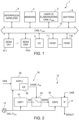
- FIG. 2 illustrates a simplified block diagram of one of the slave devices, here indicated with 13.
- the slave device 13 may be for example one of the sensors 10.1, ..., 10.N and operates on the basis of a local clock frequency F CKJ .
- F CKJ local clock frequency
- the case is illustrated by way of non-limiting example and it is understood that the synchronization technique described below may be used in devices of any type, not only with microelectromechanical sensors or with any other of the devices of the system 1.
- the slave device 13 is a synchronizing digital device according to an embodiment of the present invention and comprises a local oscillator 14, a first processing stage 15, a second processing stage 16, an interface 17 and a synchronization stage 18.
- the oscillator 14 produces a local clock signal CKJ which has the local clock frequency F CKJ and is used to time the other components of the slave device 13.
- the Figures show that the local clock signal CKJ is sent to all components of the slave device 13. It is however understood that each component may be timed with a respective clock signal obtained from the local clock signal CKJ, but not necessarily equal.
- the clock signal of each component may be defined according to design preferences and is, normally, obtained from the local clock signal CKJ by frequency division according to an integer number.
- the first processing stage 15 provides digital signals SD and may comprise or interact with a microelectromechanical structure (for example in the case of microelectromechanical inertial sensors), accomplishing generic functions provided for the correct operation of the slave device 13.
- a microelectromechanical gyroscope the first processing stage 15 may include a microstructure, actuation circuits to drive the microstructure, an analog-to-digital converter, a conversion chain to transduce movements of the microstructure correlated to a quantity to be sensed into usable electrical quantities.
- the first processing stage may be purely digital and may be provided with an interface coupled with the microstructure to receive sensing signals.
- the first processing stage 15 may include a DSP (Digital Signal Processor). The functionalities implemented by the first processing stage 15 are however determined on the basis of design preferences.
- DSP Digital Signal Processor
- the second processing stage 16 may perform further processing steps downstream of the intervention of the synchronization stage 18.
- the second processing stage 16 may also include a DSP.
- the interface 17 is coupled to the second processing stage 16 and to the system bus 12.
- the interface 17 is controlled by one or more bus clock signals CKB based on the bus clock frequency F CKB and makes available samples of output signals SOUT for the transmission through the system bus 12.
- the synchronization stage 18 is based on a multi-bit sigma-delta modulator 20 and comprises, in addiction, a reference input and a resampler stage 22 controlled by the sigma-delta modulator 20 which is included in an All Digital Phase Locked Loop (ADPLL), as explained in detail hereinbelow.
- ADPLL All Digital Phase Locked Loop
- the resampler 22 is arranged between the first processing stage 15 and the second processing stage 16 or, in case the second processing stage is not present, directly between the first processing stage 15 and the interface 17. In practice, the resampler 22 makes available resampled digital signals SDRS to the second processing stage 16.
- the resampled digital signals SDRS are obtained by taking samples of the digital signals SD supplied by the first processing stage 15 with a resampling frequency F RS and a resampling phase ⁇ RS determined by the sigma-delta modulator 20 in a manner synchronized with the bus clock frequency F CKB of the bus clock signal CKB.
- the reference input of the synchronization stage 18 is configured to be connected to the system bus 12 and receive the bus clock signal CKB based on the bus clock frequency F CKB .
- the sigma-delta modulator 20 controls the resampler 22 through a resampling signal SRS as a function of the bus clock signal CKB and modulates the resampling phase ⁇ RS so that, on average, the resampling frequency F RS coincides with the bus clock frequency F CKB .
- the oversampling carried out by the sigma-delta modulator 20 allows, on the one hand, the resampling instants to be selected through the resampler 22 and the bus clock frequency F CKB to be tracked and, on the other hand, the sampling noise to be shifted to high frequency due to the noise shaping effect associated with the sigma-delta modulators.
- the high-frequency noise may thus be effectively filtered, avoiding aliasing phenomena in the bandwidth of the digital signal SD provided by the first processing stage 15.
- Other advantages depend on the very simple structure of the sigma-delta modulators, which allows manufacturing costs to be reduced, without the need for precision analog circuits and without affecting the performances.
- the slave device 13 uses a single clock signal generated internally as the basis for the timing of all components.
- the bus clock signal CKB is used solely as a reference for the sigma-delta modulator, but it is not necessary for timing the components of the slave device 13.
- the sigma-delta modulator 20 is included in an all digital phase locked loop 25, as shown schematically in Figure 2 and in more detail in Figure 3 .
- the all digital phase locked loop 25 uses the bus clock signal CKB as a reference and in one embodiment comprises a resynchronizer 26, a phase error detector 27, a digital filter 28, the sigma-delta modulator 20, a first counter 30 and a second counter 31.
- the resynchronizer 26 receives the bus clock signal CKB at input and is configured to make available the values of the bus clock signal CKB at the local clock frequency F CKJ .
- the resynchronizer 26 comprises a D-type flip-flop which receives the bus clock signal CKB on a data input 26a and the local clock signal CKJ, or a clock signal obtained from the local clock signal CKJ for example through a frequency divider (not shown), on a clock input 26b.
- the data input 26a defines the reference input of the synchronization stage 18. In some embodiments, the resynchronization stage may be missing.
- the phase error detector 27 receives the samples of the bus clock signal CKB output from the resynchronizer 26 and, in addition, a loop clock signal CKL from the second counter 31. The phase error detector 27 determines a phase error ⁇ E between the samples of the bus clock signal CKB and the loop clock signal CKL.
- the digital filter 28 determines a signal indicative of a frequency ratio R between the bus clock frequency F CKB and the local clock frequency F CKJ of the local clock signal CKJ to be set to synchronize the slave device 13 to the system bus 12.
- the digital filter 28 may implement a proportional-integral controller.
- the sigma-delta modulator 20 converts the frequency ratio R into a relatively high-frequency and low-resolution signal that defines an approximating frequency ratio R'.
- the approximating frequency ratio R' represents in practice an integer that approximates the actual frequency ratio R, is updated to the work frequency of the sigma-delta modulator 20 and oscillates around the actual frequency ratio R.
- the approximating frequency ratio R' follows on average very precisely the actual frequency ratio R, also owing to the work frequency of the sigma-delta modulator 20, which is higher with respect to the frequency of the other signals in the all digital phase locked loop 25.
- the approximating frequency ratio R' is provided to the first counter 30 and defines a variable count limit to generate the resampling signal CKRS with modulated frequency which is on average equal to the bus clock frequency F CKB .
- the first counter 30 is a high-frequency counter and uses the highest frequency clock signal available within the slave device 13, i.e. the local clock signal CKJ.
- the resampling signal CKRS is used to both request the sigma-delta modulator 20 an updated value of the approximating frequency ratio R' and control the resampler 22.
- the first counter 30 provides the resampling signal CKRS to the sigma-delta modulator 20 through the second counter 31, the phase error detector 27 and the digital filter 28 and the sigma-delta modulator 20 provides an updated value of the approximating frequency ratio R' to the first counter 30 in response to transitions of the resampling signal CKRS.
- the resampling signal CKRS controls the resampler 22 so that the second processing stage 16 takes the value of a sample present on the output of the first processing stage 15 with resampling frequency F RS and resampling phase ⁇ RS which, on average, accurately approximate the bus clock frequency F CKB and its phase ⁇ B .
- the high count frequency of the first counter 20 and the update rate of the sigma-delta modulator 20 allow obtaining a number of samples sufficiently high so that the averages of the resampling frequency F RS and of the resampling phase ⁇ RS are effectively close to the bus clock frequency F CKB and its phase ⁇ B .
- the resampling signal CKRS is provided to the second counter 31, which generates the loop clock signal CKL.
- the second counter 31 may be for example a fixed count module counter and may operate with a clock signal at a lower frequency with respect to the first counter 30.
- the count module is defined so that the loop clock signal CKL has a frequency resulting close to the bus clock frequency F CKB of the bus clock signal CKB, to allow the phase locking.
- the second counter 31 may be a dedicated component included in the all digital phase locked loop 25 or a shared component, already present for example in the second processing stage 16.
- the invention advantageously allows using only clock signals internal to the slave devices to obtain synchronization with an external clock signal, in particular of a system bus wherewith the slave devices need to communicate.
- the resampling process and the subsequent processing steps occur in the same clock domain as the data generation.
- all the clock signals used for signal processing and for the resampling process may be obtained from the same local clock signal.
- the same performances may also be obtained by using clock frequencies which are on average lower, also to the advantage of consumption reduction and greater autonomy for portable devices.
- bus clock signals bits clock signals, word clock signals
- the bus clock signals are used only for data extraction through the interface 17.
- phase-locked loop ensures, once the phase locking is achieved, that the resampling of the signals provided by the first processing stage is performed without asynchronies. Furthermore, the frequency response of a phase-locked loop generally follows the model of a low-pass filter and allows eliminating the quantization noise of the sigma-delta modulator, which, due to the noise shaping effect, is mainly shifted to high frequency. The fact that the sigma-delta modulator is included in the phase-locked loop therefore entails a further important advantage.
- the solution proposed according to the invention is completely digital and has no impact on the analog blocks present in the slave devices.
Landscapes
- Engineering & Computer Science (AREA)
- Computer Networks & Wireless Communication (AREA)
- Signal Processing (AREA)
- Compression, Expansion, Code Conversion, And Decoders (AREA)
Abstract
Description
- The present invention relates to a synchronizing digital device.
- As is known, many electronic systems include a plurality of devices which operate at respective distinct clock frequencies, but need to communicate with each other or with a central device through a same line using a global clock. For example, it is by now extremely common to equip portable apparatuses such as smartphones, tablets and laptop computers with inertial sensors, in particular accelerometers and gyroscopes, and with other sensors, such as temperature sensors and pressure sensors, in order to extend the available functionalities. The sensors are normally connected to a central control unit, which acts as a system master, through a bus. The bus operates at a master clock frequency set for example by the control unit, while the sensors, which communicate in slave mode, each generate data with a respective native generation rate determined, inter alia, by an internal clock frequency. However, the native generation rates are generally different from each other and from the master clock frequency.
- In general, in order for the data to be exchanged between a master device and slave devices through a common line, generated data need to be synchronized with the master clock frequency, as occurs for example in systems based on Time Division Multiplexing (TDM). TDM interfaces allow the transmission of different data channels on a single line, but they are not standardized and data to be transmitted are generated in an asynchronous manner with respect to the master clock.
- Different measures may be used to obtain the synchronization, but known solutions have some limitations and may not be satisfactory.
- In accordance with a first known solution, a high-frequency master clock signal is sent to all slave devices and in practice replaces the clock signals generated by the local oscillators. The solution is robust, but represents a complication from the construction point of view, because it is necessary to add a high-frequency line to the system, and the power consumption increases in a non-negligible manner. This aspect is particularly unwanted, because it may limit the autonomy of the portable apparatuses. Furthermore, the solution cannot be applied to all devices, for example some multiaxial gyroscopes.
- According to a different solution, a resampling is carried out within the slave devices using "slow" signals of the data bus as a basis. Also in this case, however, there are some limitations. Firstly, it is necessary to provide for a conversion chain with frequency multiplication, interpolation, decimation, without however always being able to obtain the desired frequency with precision. Therefore, in the face of an increase in circuit complexity, the result may not be optimal. Furthermore, the conversion and resampling operations introduce noise in the form of spectral peaks that may degrade the signal.
- The aim of the present invention is to provide a synchronizing digital device which allows the limitations described to be overcome or at least mitigated.
- According to the present invention a synchronizing digital device is provided as defined in
claim 1. - For a better understanding of the invention, an embodiment thereof will now be described, purely by way of non-limiting example and with reference to the attached drawings, wherein:
-
Figure 1 is a simplified block diagram of an electronic system; -
Figure 2 is a block diagram of a synchronizing digital device according to an embodiment of the present invention incorporated in the system ofFigure 1 ; and -
Figure 3 is a more detailed block diagram of a part of the synchronizing digital device ofFigure 2 . - With reference to
Figure 1 , an electronic system is indicated as a whole with thenumber 1 and may be an electronic system of any type, in particular, but not limited to, a wearable device, such as a watch, a bracelet or a smart band; a computer, such as a mainframe, a personal computer, a laptop or a tablet; a smartphone; a digital music player, a digital camera or any other device for processing, storing, transmitting or receiving information. Theelectronic system 1 may be a general purpose or device-embedded processing system, an equipment or a further system. - The
electronic system 1 may comprise aprocessing unit 2,memory devices 3, input/output (I/O) devices 5 (for example a keyboard, a pointer or a touch screen), awireless interface 6, peripherals 7.1, ..., 7.N, abattery 8 and possibly further auxiliary devices, not shown here. Theprocessing unit 2 may comprise, for example, one or more microprocessors, microcontrollers and the like, according to design preferences. - Furthermore, the
electronic system 1 may comprise one or more sensors 10.1, ..., 10.N, for example accelerometers, gyroscopes, pressure sensors, temperature sensors, humidity sensors. The sensors 10.1, ..., 10.N may be of microelectromechanical type. - It is to be noted that the scope of the present invention is not limited to embodiments necessarily having one or all of the devices listed.
- The components of the
electronic system 1 may be coupled in communication with each other and in particular to theprocessing unit 2 through asystem bus 12, which is global as in the example ofFigure 1 , or through local buses dedicated to groups of devices, for example the sensors 10.1, ..., 10.N. One of the components, normally theprocessing unit 2, acts as a master and the other components, for example the sensors 10.1, ..., 10.N, are coupled in communication through thesystem bus 12 in slave mode. - At least some of the slave devices of the system 1 (
Figure 2 ), including for example the sensors 10.1, ..., 10.N, are configured to provide data based on local oscillators with respective local clock frequencies FCK1, ..., FCKN asynchronous to each other and asynchronous with respect to a bus clock frequency FCKB of thebus 12. The bus clock frequency FCKB of thebus 12 may for example be set by theprocessing unit 2, which acts as a master, and may be determined on the basis of a master clock frequency FCKM of the same processing unit 2 (typically, the master clock frequency FCKM is an integer multiple of the bus clock frequency FCKB). -
Figure 2 illustrates a simplified block diagram of one of the slave devices, here indicated with 13. Theslave device 13 may be for example one of the sensors 10.1, ..., 10.N and operates on the basis of a local clock frequency FCKJ. The case is illustrated by way of non-limiting example and it is understood that the synchronization technique described below may be used in devices of any type, not only with microelectromechanical sensors or with any other of the devices of thesystem 1. - The
slave device 13 is a synchronizing digital device according to an embodiment of the present invention and comprises alocal oscillator 14, afirst processing stage 15, asecond processing stage 16, aninterface 17 and asynchronization stage 18. - The
oscillator 14 produces a local clock signal CKJ which has the local clock frequency FCKJ and is used to time the other components of theslave device 13. For the sake of simplicity, the Figures show that the local clock signal CKJ is sent to all components of theslave device 13. It is however understood that each component may be timed with a respective clock signal obtained from the local clock signal CKJ, but not necessarily equal. The clock signal of each component may be defined according to design preferences and is, normally, obtained from the local clock signal CKJ by frequency division according to an integer number. - The
first processing stage 15 provides digital signals SD and may comprise or interact with a microelectromechanical structure (for example in the case of microelectromechanical inertial sensors), accomplishing generic functions provided for the correct operation of theslave device 13. For example, in a microelectromechanical gyroscope thefirst processing stage 15 may include a microstructure, actuation circuits to drive the microstructure, an analog-to-digital converter, a conversion chain to transduce movements of the microstructure correlated to a quantity to be sensed into usable electrical quantities. Alternatively, the first processing stage may be purely digital and may be provided with an interface coupled with the microstructure to receive sensing signals. Thefirst processing stage 15 may include a DSP (Digital Signal Processor). The functionalities implemented by thefirst processing stage 15 are however determined on the basis of design preferences. - The
second processing stage 16, if any, may perform further processing steps downstream of the intervention of thesynchronization stage 18. Thesecond processing stage 16 may also include a DSP. - The
interface 17 is coupled to thesecond processing stage 16 and to thesystem bus 12. In particular, theinterface 17 is controlled by one or more bus clock signals CKB based on the bus clock frequency FCKB and makes available samples of output signals SOUT for the transmission through thesystem bus 12. - In one embodiment, the
synchronization stage 18 is based on a multi-bit sigma-delta modulator 20 and comprises, in addiction, a reference input and aresampler stage 22 controlled by the sigma-delta modulator 20 which is included in an All Digital Phase Locked Loop (ADPLL), as explained in detail hereinbelow. Theresampler 22 is arranged between thefirst processing stage 15 and thesecond processing stage 16 or, in case the second processing stage is not present, directly between thefirst processing stage 15 and theinterface 17. In practice, theresampler 22 makes available resampled digital signals SDRS to thesecond processing stage 16. The resampled digital signals SDRS are obtained by taking samples of the digital signals SD supplied by thefirst processing stage 15 with a resampling frequency FRS and a resampling phase ϕRS determined by the sigma-delta modulator 20 in a manner synchronized with the bus clock frequency FCKB of the bus clock signal CKB. - The reference input of the
synchronization stage 18 is configured to be connected to thesystem bus 12 and receive the bus clock signal CKB based on the bus clock frequency FCKB. - The sigma-
delta modulator 20 controls theresampler 22 through a resampling signal SRS as a function of the bus clock signal CKB and modulates the resampling phase ϕRS so that, on average, the resampling frequency FRS coincides with the bus clock frequency FCKB. In practice, the oversampling carried out by the sigma-delta modulator 20 allows, on the one hand, the resampling instants to be selected through theresampler 22 and the bus clock frequency FCKB to be tracked and, on the other hand, the sampling noise to be shifted to high frequency due to the noise shaping effect associated with the sigma-delta modulators. The high-frequency noise may thus be effectively filtered, avoiding aliasing phenomena in the bandwidth of the digital signal SD provided by thefirst processing stage 15. Other advantages depend on the very simple structure of the sigma-delta modulators, which allows manufacturing costs to be reduced, without the need for precision analog circuits and without affecting the performances. Furthermore, theslave device 13 uses a single clock signal generated internally as the basis for the timing of all components. The bus clock signal CKB is used solely as a reference for the sigma-delta modulator, but it is not necessary for timing the components of theslave device 13. - To obtain the correct ratio between the bus clock frequency FCKB and the resampling frequency FRS by operating in the domain of the local clock frequency FCKJ, the sigma-
delta modulator 20 is included in an all digital phase lockedloop 25, as shown schematically inFigure 2 and in more detail inFigure 3 . The all digital phase lockedloop 25 uses the bus clock signal CKB as a reference and in one embodiment comprises aresynchronizer 26, aphase error detector 27, adigital filter 28, the sigma-delta modulator 20, afirst counter 30 and asecond counter 31. - The
resynchronizer 26 receives the bus clock signal CKB at input and is configured to make available the values of the bus clock signal CKB at the local clock frequency FCKJ. In one embodiment, theresynchronizer 26 comprises a D-type flip-flop which receives the bus clock signal CKB on adata input 26a and the local clock signal CKJ, or a clock signal obtained from the local clock signal CKJ for example through a frequency divider (not shown), on aclock input 26b. Thedata input 26a defines the reference input of thesynchronization stage 18. In some embodiments, the resynchronization stage may be missing. - The
phase error detector 27 receives the samples of the bus clock signal CKB output from theresynchronizer 26 and, in addition, a loop clock signal CKL from thesecond counter 31. Thephase error detector 27 determines a phase error ϕE between the samples of the bus clock signal CKB and the loop clock signal CKL. - Based on the phase error ϕE from the
phase error detector 27 provided by thephase error detector 27, thedigital filter 28 determines a signal indicative of a frequency ratio R between the bus clock frequency FCKB and the local clock frequency FCKJ of the local clock signal CKJ to be set to synchronize theslave device 13 to thesystem bus 12. In a limiting embodiment, for example, thedigital filter 28 may implement a proportional-integral controller. - The sigma-
delta modulator 20 converts the frequency ratio R into a relatively high-frequency and low-resolution signal that defines an approximating frequency ratio R'. The approximating frequency ratio R' represents in practice an integer that approximates the actual frequency ratio R, is updated to the work frequency of the sigma-delta modulator 20 and oscillates around the actual frequency ratio R. The approximating frequency ratio R' follows on average very precisely the actual frequency ratio R, also owing to the work frequency of the sigma-delta modulator 20, which is higher with respect to the frequency of the other signals in the all digital phase lockedloop 25. - The approximating frequency ratio R' is provided to the
first counter 30 and defines a variable count limit to generate the resampling signal CKRS with modulated frequency which is on average equal to the bus clock frequency FCKB. Thefirst counter 30 is a high-frequency counter and uses the highest frequency clock signal available within theslave device 13, i.e. the local clock signal CKJ. - The resampling signal CKRS is used to both request the sigma-
delta modulator 20 an updated value of the approximating frequency ratio R' and control theresampler 22. In practice, thefirst counter 30 provides the resampling signal CKRS to the sigma-delta modulator 20 through thesecond counter 31, thephase error detector 27 and thedigital filter 28 and the sigma-delta modulator 20 provides an updated value of the approximating frequency ratio R' to thefirst counter 30 in response to transitions of the resampling signal CKRS. - The resampling signal CKRS controls the
resampler 22 so that thesecond processing stage 16 takes the value of a sample present on the output of thefirst processing stage 15 with resampling frequency FRS and resampling phase ϕRS which, on average, accurately approximate the bus clock frequency FCKB and its phase ϕB. More precisely, the high count frequency of thefirst counter 20 and the update rate of the sigma-delta modulator 20 allow obtaining a number of samples sufficiently high so that the averages of the resampling frequency FRS and of the resampling phase ϕRS are effectively close to the bus clock frequency FCKB and its phase ϕB. - Furthermore, the resampling signal CKRS is provided to the
second counter 31, which generates the loop clock signal CKL. Thesecond counter 31 may be for example a fixed count module counter and may operate with a clock signal at a lower frequency with respect to thefirst counter 30. The count module is defined so that the loop clock signal CKL has a frequency resulting close to the bus clock frequency FCKB of the bus clock signal CKB, to allow the phase locking. Thesecond counter 31 may be a dedicated component included in the all digital phase lockedloop 25 or a shared component, already present for example in thesecond processing stage 16. - The invention advantageously allows using only clock signals internal to the slave devices to obtain synchronization with an external clock signal, in particular of a system bus wherewith the slave devices need to communicate. In fact, the resampling process and the subsequent processing steps occur in the same clock domain as the data generation. In other words, except for the bus frequency reference to be locked, all the clock signals used for signal processing and for the resampling process may be obtained from the same local clock signal. The same performances may also be obtained by using clock frequencies which are on average lower, also to the advantage of consumption reduction and greater autonomy for portable devices.
- For the implementation of communication schemes based on time division multiplexing, for example, the bus clock signals (bit clock signals, word clock signals) are used only for data extraction through the
interface 17. - The use of the phase-locked loop ensures, once the phase locking is achieved, that the resampling of the signals provided by the first processing stage is performed without asynchronies. Furthermore, the frequency response of a phase-locked loop generally follows the model of a low-pass filter and allows eliminating the quantization noise of the sigma-delta modulator, which, due to the noise shaping effect, is mainly shifted to high frequency. The fact that the sigma-delta modulator is included in the phase-locked loop therefore entails a further important advantage.
- Furthermore, the solution proposed according to the invention is completely digital and has no impact on the analog blocks present in the slave devices.
- Finally, it is clear that modifications and variations may be made to the device described, without departing from the scope of the present invention, as defined in the attached claims.
Claims (15)
- A synchronizing digital device comprising:a reference input (26a) configured to receive a reference clock signal (CKB), having a reference clock frequency (FCKB);an output (17);a local oscillator (14), providing a local clock signal (CKJ) having a local clock frequency (FCKJ);a digital signal source (15), based on the local clock signal (CKJ) and providing digital signals (SD); anda synchronization stage (18), based on the local clock signal (CKJ) and comprising:a resampler (22), arranged between the digital signal source (15) and the output (17) and configured to make available resampled digital signals (SDRS), obtained by taking samples of the digital signals (SD) with a resampling frequency (FRS); anda sigma-delta modulator (20) configured to cause the generation of a resampling signal (CKF) modulated on average at the resampling frequency (FRS) as a function of the reference clock signal (CKB) and to control the resampler (22) through the resampling signal (CKF).
- The device according to claim 1, wherein the synchronization stage (18) comprises an all digital phase locked loop (25), receiving the reference clock signal (CKB) and including the sigma-delta modulator (20).
- The device according to claim 2, wherein the all digital phase locked loop (25) comprises a phase error detector (27) receiving the reference clock signal (CKB) and a loop clock signal (CKL) obtained from the resampling signal (CKRS) and configured to generate a phase error signal (ϕE) based on the reference clock signal (CKB) and the loop clock signal (CKL).
- The device according to claim 3, wherein the all digital phase locked loop (25) comprises a digital filter (28), configured to generate a frequency ratio (R) indicative of a ratio between the bus clock frequency (FCKB) and the local clock frequency (FCKJ) of the local clock signal (CKJ) on the basis of the phase error signal (ϕE).
- The device according to claim 4, wherein the sigma-delta modulator (20) is a multi-bit modulator configured to generate an approximating frequency ratio (R') from the frequency ratio (R), so that the approximating frequency ratio (R') is on average equal to the frequency ratio (R).
- The device according to claim 5, wherein the all digital phase locked loop (25) comprises a first counter (30) coupled to the sigma-delta modulator (20) to receive the approximating frequency ratio (R'), wherein the approximating frequency ratio (R') defines a variable count limit for the first counter (30).
- The device according to claim 6, wherein the first counter (30) is configured to generate the resampling signal (CKF) as a function of the approximating frequency ratio (R').
- The device according to claim 6 or 7, wherein the first counter (30) is a high-frequency counter based on a clock signal at maximum available frequency.
- The device according to any of claims 6 to 8, wherein the first counter (30) is configured to control the resampler (22) by the resampling signal (CKRS).
- The device according to any of claims 6 to 9, wherein the first counter (30) is configured to provide the resampling signal (CKRS) to the sigma-delta modulator (20) and the sigma-delta modulator (20) is configured to provide an updated value of the approximating frequency ratio (R') to the first counter (30) in response to transitions of the resampling signal (CKRS).
- The device according to any of claims 6 to 10, wherein the all digital phase locked loop (25) comprises a second counter (31) coupled to the first counter (30) to receive the resampling signal (CKRS) and configured to generate the loop clock signal (CKL) at a loop clock frequency (FCKL) lower than the resampling frequency (FRS).
- The device according to claim 11, wherein the second counter (31) is coupled to the phase error detector (27) to provide the loop clock signal (CKL).
- The device according to any of claims 3 to 12, comprising a resynchronizer (26) configured to receive the reference clock signal (CKB) and configured to make available values of the reference clock signal (CKB) at the local clock frequency (FCKJ) or at frequency obtained from the local clock frequency (FCKJ).
- The device according to any of the preceding claims, comprising a digital processing stage (16) arranged between the resampler (22) and the output (17) and configured to receive the resampled digital signals (SDRS) from the resampler (22).
- An electronic system comprising a master device (2), a bus (12) and at least one synchronizing digital device (10.1, ..., 10.N; 13) according to any of the preceding claims, configured to communicate with the master device (2) in slave mode through the bus (12); wherein the reference clock signal (CKB) is defined by a bus clock signal of the bus (12).
Applications Claiming Priority (1)
| Application Number | Priority Date | Filing Date | Title |
|---|---|---|---|
| IT102022000016557A IT202200016557A1 (en) | 2022-08-03 | 2022-08-03 | DIGITAL SYNCHRONIZING DEVICE |
Publications (3)
| Publication Number | Publication Date |
|---|---|
| EP4319039A1 true EP4319039A1 (en) | 2024-02-07 |
| EP4319039A9 EP4319039A9 (en) | 2024-03-20 |
| EP4319039B1 EP4319039B1 (en) | 2025-10-01 |
Family
ID=83691360
Family Applications (1)
| Application Number | Title | Priority Date | Filing Date |
|---|---|---|---|
| EP23186442.2A Active EP4319039B1 (en) | 2022-08-03 | 2023-07-19 | Synchronizing digital device |
Country Status (3)
| Country | Link |
|---|---|
| US (1) | US12267078B2 (en) |
| EP (1) | EP4319039B1 (en) |
| IT (1) | IT202200016557A1 (en) |
Citations (3)
| Publication number | Priority date | Publication date | Assignee | Title |
|---|---|---|---|---|
| WO1995008220A1 (en) * | 1993-09-13 | 1995-03-23 | Analog Devices, Inc. | Analog to digital conversion using nonuniform sample rates |
| WO1997013325A1 (en) * | 1995-10-05 | 1997-04-10 | Analog Devices, Inc. | Variable sample-rate dac/adc/converter system |
| US20090160564A1 (en) * | 2007-12-20 | 2009-06-25 | Seonghwan Cho | Enhanced all digital phase-locked loop and oscillation signal generation method thereof |
-
2022
- 2022-08-03 IT IT102022000016557A patent/IT202200016557A1/en unknown
-
2023
- 2023-07-14 US US18/352,581 patent/US12267078B2/en active Active
- 2023-07-19 EP EP23186442.2A patent/EP4319039B1/en active Active
Patent Citations (3)
| Publication number | Priority date | Publication date | Assignee | Title |
|---|---|---|---|---|
| WO1995008220A1 (en) * | 1993-09-13 | 1995-03-23 | Analog Devices, Inc. | Analog to digital conversion using nonuniform sample rates |
| WO1997013325A1 (en) * | 1995-10-05 | 1997-04-10 | Analog Devices, Inc. | Variable sample-rate dac/adc/converter system |
| US20090160564A1 (en) * | 2007-12-20 | 2009-06-25 | Seonghwan Cho | Enhanced all digital phase-locked loop and oscillation signal generation method thereof |
Non-Patent Citations (1)
| Title |
|---|
| URBANSKY R ET AL: "A NOVEL SLAVE-CLOCK IMPLEMENTATION APPROACH FOR TELECOMMUNICATIONS NETWORK SYNCHRONISATION", PROCEEDINGS OF THE EUROPEAN FREQUENCY AND TIME FORUM, XX, XX, no. 418, 5 March 1996 (1996-03-05), pages 534 - 539, XP000955628 * |
Also Published As
| Publication number | Publication date |
|---|---|
| US20240048144A1 (en) | 2024-02-08 |
| EP4319039A9 (en) | 2024-03-20 |
| US12267078B2 (en) | 2025-04-01 |
| EP4319039B1 (en) | 2025-10-01 |
| IT202200016557A1 (en) | 2024-02-03 |
Similar Documents
| Publication | Publication Date | Title |
|---|---|---|
| CN113346906B (en) | Quantization Error Reduction Technique for Fractional-N Phase-Locked Loops Using Σ-Δ Modulation | |
| TWI775988B (en) | Phase locked loop electronic circuit, electronic device using the same and method for correcting duty cycle | |
| CN107918444B (en) | Phase Control Based on Feedback Clock Signal | |
| JP5021871B2 (en) | Digital small phase detector | |
| JP5286845B2 (en) | Data recovery circuit | |
| US8964922B2 (en) | Adaptive frequency synthesis for a serial data interface | |
| JP2005223829A (en) | Fractional frequency divider circuit and data transmission apparatus using the same | |
| CN102315927A (en) | Clock synchronization device and method | |
| US9429980B2 (en) | Flexible clocking for audio sample rate converter in a USB system | |
| KR100195855B1 (en) | Clock synchronization scheme for fractional multiplication systems | |
| CN104579328B (en) | Oscillating circuit, oscillator, electronic equipment and moving body | |
| CN1697324B (en) | Implementation method and device for transmission signal dejittering | |
| US8767898B2 (en) | Method and system of synchronizing data to reference time signal with data resampling | |
| EP4319039A9 (en) | Synchronizing digital device | |
| JP7488104B2 (en) | Timing Synchronization Circuit | |
| CN101502036B (en) | Semiconductor integrated circuit and transmitting device having the same | |
| CN111837339B (en) | Phase-locked loop circuit and equipment using phase-locked loop circuit | |
| JP2020182198A (en) | Time synchronization measurement system | |
| CN117526933A (en) | Sync digital devices | |
| JPWO2009069244A1 (en) | Transmission method and transmission apparatus | |
| CN120880435B (en) | A PLL layout structure for MCU chips | |
| JP2025075253A (en) | Data Processing Unit | |
| US5943373A (en) | External protocol hooks system and method | |
| US20250141653A1 (en) | Electronic digital system comprising a serializer deserializer module, serializer deserializer module and method of control | |
| JP2011211676A (en) | Single clock sharing type computer system |
Legal Events
| Date | Code | Title | Description |
|---|---|---|---|
| PUAI | Public reference made under article 153(3) epc to a published international application that has entered the european phase |
Free format text: ORIGINAL CODE: 0009012 |
|
| STAA | Information on the status of an ep patent application or granted ep patent |
Free format text: STATUS: THE APPLICATION HAS BEEN PUBLISHED |
|
| AK | Designated contracting states |
Kind code of ref document: A1 Designated state(s): AL AT BE BG CH CY CZ DE DK EE ES FI FR GB GR HR HU IE IS IT LI LT LU LV MC ME MK MT NL NO PL PT RO RS SE SI SK SM TR |
|
| STAA | Information on the status of an ep patent application or granted ep patent |
Free format text: STATUS: REQUEST FOR EXAMINATION WAS MADE |
|
| 17P | Request for examination filed |
Effective date: 20240807 |
|
| RBV | Designated contracting states (corrected) |
Designated state(s): AL AT BE BG CH CY CZ DE DK EE ES FI FR GB GR HR HU IE IS IT LI LT LU LV MC ME MK MT NL NO PL PT RO RS SE SI SK SM TR |
|
| GRAP | Despatch of communication of intention to grant a patent |
Free format text: ORIGINAL CODE: EPIDOSNIGR1 |
|
| STAA | Information on the status of an ep patent application or granted ep patent |
Free format text: STATUS: GRANT OF PATENT IS INTENDED |
|
| INTG | Intention to grant announced |
Effective date: 20250424 |
|
| GRAS | Grant fee paid |
Free format text: ORIGINAL CODE: EPIDOSNIGR3 |
|
| GRAA | (expected) grant |
Free format text: ORIGINAL CODE: 0009210 |
|
| STAA | Information on the status of an ep patent application or granted ep patent |
Free format text: STATUS: THE PATENT HAS BEEN GRANTED |
|
| AK | Designated contracting states |
Kind code of ref document: B1 Designated state(s): AL AT BE BG CH CY CZ DE DK EE ES FI FR GB GR HR HU IE IS IT LI LT LU LV MC ME MK MT NL NO PL PT RO RS SE SI SK SM TR |
|
| REG | Reference to a national code |
Ref country code: GB Ref legal event code: FG4D Ref country code: CH Ref legal event code: F10 Free format text: ST27 STATUS EVENT CODE: U-0-0-F10-F00 (AS PROVIDED BY THE NATIONAL OFFICE) Effective date: 20251001 |
|
| REG | Reference to a national code |
Ref country code: IE Ref legal event code: FG4D |
|
| REG | Reference to a national code |
Ref country code: DE Ref legal event code: R096 Ref document number: 602023007078 Country of ref document: DE |
|
| REG | Reference to a national code |
Ref country code: NL Ref legal event code: MP Effective date: 20251001 |
|
| REG | Reference to a national code |
Ref country code: AT Ref legal event code: MK05 Ref document number: 1843701 Country of ref document: AT Kind code of ref document: T Effective date: 20251001 |
|
| PG25 | Lapsed in a contracting state [announced via postgrant information from national office to epo] |
Ref country code: NL Free format text: LAPSE BECAUSE OF FAILURE TO SUBMIT A TRANSLATION OF THE DESCRIPTION OR TO PAY THE FEE WITHIN THE PRESCRIBED TIME-LIMIT Effective date: 20251001 |
|
| PG25 | Lapsed in a contracting state [announced via postgrant information from national office to epo] |
Ref country code: ES Free format text: LAPSE BECAUSE OF FAILURE TO SUBMIT A TRANSLATION OF THE DESCRIPTION OR TO PAY THE FEE WITHIN THE PRESCRIBED TIME-LIMIT Effective date: 20251001 |
|
| REG | Reference to a national code |
Ref country code: LT Ref legal event code: MG9D |
|
| PG25 | Lapsed in a contracting state [announced via postgrant information from national office to epo] |
Ref country code: NO Free format text: LAPSE BECAUSE OF FAILURE TO SUBMIT A TRANSLATION OF THE DESCRIPTION OR TO PAY THE FEE WITHIN THE PRESCRIBED TIME-LIMIT Effective date: 20260101 |
|
| PG25 | Lapsed in a contracting state [announced via postgrant information from national office to epo] |
Ref country code: AT Free format text: LAPSE BECAUSE OF FAILURE TO SUBMIT A TRANSLATION OF THE DESCRIPTION OR TO PAY THE FEE WITHIN THE PRESCRIBED TIME-LIMIT Effective date: 20251001 Ref country code: FI Free format text: LAPSE BECAUSE OF FAILURE TO SUBMIT A TRANSLATION OF THE DESCRIPTION OR TO PAY THE FEE WITHIN THE PRESCRIBED TIME-LIMIT Effective date: 20251001 Ref country code: HR Free format text: LAPSE BECAUSE OF FAILURE TO SUBMIT A TRANSLATION OF THE DESCRIPTION OR TO PAY THE FEE WITHIN THE PRESCRIBED TIME-LIMIT Effective date: 20251001 |
|
| PG25 | Lapsed in a contracting state [announced via postgrant information from national office to epo] |
Ref country code: RS Free format text: LAPSE BECAUSE OF FAILURE TO SUBMIT A TRANSLATION OF THE DESCRIPTION OR TO PAY THE FEE WITHIN THE PRESCRIBED TIME-LIMIT Effective date: 20260101 |
|
| PG25 | Lapsed in a contracting state [announced via postgrant information from national office to epo] |
Ref country code: IS Free format text: LAPSE BECAUSE OF FAILURE TO SUBMIT A TRANSLATION OF THE DESCRIPTION OR TO PAY THE FEE WITHIN THE PRESCRIBED TIME-LIMIT Effective date: 20260201 |
|
| PG25 | Lapsed in a contracting state [announced via postgrant information from national office to epo] |
Ref country code: PT Free format text: LAPSE BECAUSE OF FAILURE TO SUBMIT A TRANSLATION OF THE DESCRIPTION OR TO PAY THE FEE WITHIN THE PRESCRIBED TIME-LIMIT Effective date: 20260202 Ref country code: CZ Free format text: LAPSE BECAUSE OF FAILURE TO SUBMIT A TRANSLATION OF THE DESCRIPTION OR TO PAY THE FEE WITHIN THE PRESCRIBED TIME-LIMIT Effective date: 20251001 |
|
| PG25 | Lapsed in a contracting state [announced via postgrant information from national office to epo] |
Ref country code: PL Free format text: LAPSE BECAUSE OF FAILURE TO SUBMIT A TRANSLATION OF THE DESCRIPTION OR TO PAY THE FEE WITHIN THE PRESCRIBED TIME-LIMIT Effective date: 20251001 |
|
| PG25 | Lapsed in a contracting state [announced via postgrant information from national office to epo] |
Ref country code: LV Free format text: LAPSE BECAUSE OF FAILURE TO SUBMIT A TRANSLATION OF THE DESCRIPTION OR TO PAY THE FEE WITHIN THE PRESCRIBED TIME-LIMIT Effective date: 20251001 |
|
| PG25 | Lapsed in a contracting state [announced via postgrant information from national office to epo] |
Ref country code: BG Free format text: LAPSE BECAUSE OF FAILURE TO SUBMIT A TRANSLATION OF THE DESCRIPTION OR TO PAY THE FEE WITHIN THE PRESCRIBED TIME-LIMIT Effective date: 20251001 |