EP4318876A1 - Wireless power receiving apparatus for carrying out in-band communication with wireless power transmitting apparatus and method for carrying out in-band communication in wireless power receiving apparatus - Google Patents
Wireless power receiving apparatus for carrying out in-band communication with wireless power transmitting apparatus and method for carrying out in-band communication in wireless power receiving apparatus Download PDFInfo
- Publication number
- EP4318876A1 EP4318876A1 EP22775955.2A EP22775955A EP4318876A1 EP 4318876 A1 EP4318876 A1 EP 4318876A1 EP 22775955 A EP22775955 A EP 22775955A EP 4318876 A1 EP4318876 A1 EP 4318876A1
- Authority
- EP
- European Patent Office
- Prior art keywords
- switches
- wireless power
- capacitor
- reception device
- capacitors
- Prior art date
- Legal status (The legal status is an assumption and is not a legal conclusion. Google has not performed a legal analysis and makes no representation as to the accuracy of the status listed.)
- Pending
Links
Images




Classifications
-
- H—ELECTRICITY
- H02—GENERATION; CONVERSION OR DISTRIBUTION OF ELECTRIC POWER
- H02J—ELECTRIC POWER NETWORKS; CIRCUIT ARRANGEMENTS OR SYSTEMS FOR SUPPLYING OR DISTRIBUTING ELECTRIC POWER; SYSTEMS FOR STORING ELECTRIC ENERGY
- H02J50/00—Circuit arrangements or systems for wireless supply or distribution of electric power
- H02J50/80—Circuit arrangements or systems for wireless supply or distribution of electric power involving the exchange of data, concerning supply or distribution of electric power, between transmitting devices and receiving devices
-
- H—ELECTRICITY
- H02—GENERATION; CONVERSION OR DISTRIBUTION OF ELECTRIC POWER
- H02J—ELECTRIC POWER NETWORKS; CIRCUIT ARRANGEMENTS OR SYSTEMS FOR SUPPLYING OR DISTRIBUTING ELECTRIC POWER; SYSTEMS FOR STORING ELECTRIC ENERGY
- H02J50/00—Circuit arrangements or systems for wireless supply or distribution of electric power
- H02J50/10—Circuit arrangements or systems for wireless supply or distribution of electric power using inductive coupling
- H02J50/12—Circuit arrangements or systems for wireless supply or distribution of electric power using inductive coupling of the resonant type
-
- H—ELECTRICITY
- H04—ELECTRIC COMMUNICATION TECHNIQUE
- H04B—TRANSMISSION
- H04B5/00—Near-field transmission systems, e.g. inductive or capacitive transmission systems
- H04B5/20—Near-field transmission systems, e.g. inductive or capacitive transmission systems characterised by the transmission technique; characterised by the transmission medium
- H04B5/24—Inductive coupling
- H04B5/26—Inductive coupling using coils
- H04B5/266—One coil at each side, e.g. with primary and secondary coils
-
- H—ELECTRICITY
- H04—ELECTRIC COMMUNICATION TECHNIQUE
- H04L—TRANSMISSION OF DIGITAL INFORMATION, e.g. TELEGRAPHIC COMMUNICATION
- H04L25/00—Baseband systems
- H04L25/02—Details ; arrangements for supplying electrical power along data transmission lines
-
- H—ELECTRICITY
- H04—ELECTRIC COMMUNICATION TECHNIQUE
- H04L—TRANSMISSION OF DIGITAL INFORMATION, e.g. TELEGRAPHIC COMMUNICATION
- H04L25/00—Baseband systems
- H04L25/02—Details ; arrangements for supplying electrical power along data transmission lines
- H04L25/0264—Arrangements for coupling to transmission lines
- H04L25/0266—Arrangements for providing Galvanic isolation, e.g. by means of magnetic or capacitive coupling
- H04L25/0268—Arrangements for providing Galvanic isolation, e.g. by means of magnetic or capacitive coupling with modulation and subsequent demodulation
-
- H—ELECTRICITY
- H04—ELECTRIC COMMUNICATION TECHNIQUE
- H04B—TRANSMISSION
- H04B5/00—Near-field transmission systems, e.g. inductive or capacitive transmission systems
- H04B5/70—Near-field transmission systems, e.g. inductive or capacitive transmission systems specially adapted for specific purposes
- H04B5/79—Near-field transmission systems, e.g. inductive or capacitive transmission systems specially adapted for specific purposes for data transfer in combination with power transfer
Definitions
- Various embodiments relate to a wireless power reception device performing in-band communication with a wireless power transmission device and a method for performing in-band communication in a wireless power reception device.
- the wireless power transmission technology using the magnetic induction scheme is a scheme for transferring power by the electromagnetic field induced in the coil.
- the wireless power transmitting device applies a current to the transmission coil to generate an electromagnetic field, and an induced current is formed in the reception coil of the wireless power receiving device, so that power may be wirelessly transmitted.
- Wireless power transmission technology may contribute to convenience in that there is no need to connect the charging terminals to the electronic device.
- the wireless power reception device may transmit a signal to the wireless power transmission device through in-band communication to control the received wireless power.
- An additional resonance element may be connected to the resonance circuit of the wireless power reception device and, as the additional resonance element is connected, the current flowing through the transmission coil of the wireless power transmission device and/or the voltage across the transmission coil may change.
- the wireless power transmission device may obtain the signal by performing demodulation on the current flowing through the transmission coil and/or the voltage across the transmission coil.
- the process of changing the current flowing through the transmission coil of the wireless power transmission device and/or the voltage across the transmission coil by controlling the connection between the resonance circuit and the additional resonance element in the wireless power reception device may be referred to as a process of transmitting an in-band communication signal to the wireless power transmission device.
- the wireless power transmission device may control wireless power transmitted to the wireless power reception device based on the signal obtained from the wireless power reception device through in-band communication.
- One or more modulation capacitors for performing in-band communication may be connected to the resonance circuit of the wireless power reception device.
- the capacitance of the modulation capacitor When the capacitance of the modulation capacitor is large, the current flowing through the transmission coil of the wireless power transmission device and/or the voltage across the transmission coil may be greatly changed. In other words, when the capacitance of the modulation capacitor is large, a signal having a large amplitude may be transferred to the wireless power transmission device.
- the capacitance of the modulation capacitor is large, overshoot of the voltage output from the rectification circuit of the wireless power reception device increases, resulting in increased voltage stress in the rectification circuit and increased loss in the regulator. Further, audible noise may occur as perturbation of the audible frequency band periodically occurs in the in-band signal.
- the amplitude of the demodulation signal that may be obtained by performing demodulation on the current flowing through the transmission coil and/or the voltage across the transmission coil in the wireless power transmission device may vary depending on the load conditions and the switching frequency.
- the wireless power reception device may include a plurality of capacitors connected to the resonance circuit and may select a combination of modulation capacitors based on the control error packet (CEP) value identified based on the output of the resonance circuit.
- CEP control error packet
- a wireless power reception device may comprise a resonance circuit configured to receive wireless power from a wireless power transmission device, a plurality of first capacitors, a plurality of first switches, a plurality of second capacitors, a plurality of second switches, a rectification circuit connected to a first end and a second end of the resonance circuit, and a control circuit connected to the rectification circuit.
- Each of first ends of the plurality of first capacitors may be connected to the first end of the resonance circuit, second ends of the plurality of first capacitors may be respectively connected to first ends of the plurality of first switches, and second ends of the plurality of first switches may be connected to a ground.
- Each of first ends of the plurality of second capacitors may be connected to the second end of the resonance circuit, second ends of the plurality of second capacitors may be respectively connected to first ends of the plurality of second switches, and second ends of the plurality of second switches may be connected to the ground.
- the control circuit may be configured to select switches for modulating data to be transmitted to the wireless power transmission device among the plurality of first switches and the plurality of second switches based on a CEP value identified based on an output of the rectification circuit and control on/off of the selected switches based on modulation of the data.
- a method performed by a wireless power reception device including a resonance circuit, a plurality of first capacitors, a plurality of first switches, a plurality of second capacitors, and a plurality of second switches, wherein each of first ends of the plurality of first capacitors is connected to the first end of the resonance circuit, second ends of the plurality of first capacitors are respectively connected to first ends of the plurality of first switches, and second ends of the plurality of first switches are connected to a ground, wherein each of first ends of the plurality of second capacitors is connected to the second end of the resonance circuit, second ends of the plurality of second capacitors are respectively connected to first ends of the plurality of second switches, and second ends of the plurality of second switches are connected to the ground, may comprise identifying a CEP value based on an output of a rectification circuit of the wireless power reception device, selecting switches for modulating data to be transmitted to a wireless power transmission device among the plurality of first switches and the plurality of second switches based on the CEP value,
- a wireless power reception device performing in-band communication with a wireless power transmission device and a method for performing in-band communication in a wireless power reception device.
- the wireless power reception device may include a plurality of capacitors connected to the resonance circuit and may select a combination of modulation capacitors based on the CEP value identified based on the output of the resonance circuit.
- the wireless power reception device may determine whether wireless power is properly controlled through in-band communication based on the CEP value and, accordingly, adaptively select a combination of modulation capacitors.
- the wireless power reception device may maintain the minimum capacitance of the modulation capacitors within a range in which smooth in-band communication is possible, making it possible to minimize the voltage stress of the resonance circuit and the loss in the regulator and properly control wireless power while mitigating audible noise.
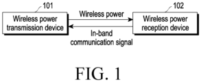
- FIG. 1 is a block diagram illustrating a wireless power transmission device and a wireless power receiving device according to various embodiments.
- a wireless power transmission device 101 may transmit wireless power to a wireless power reception device 102.
- the wireless power transmission device 101 may transmit wireless power to the wireless power reception device 102 according to an induction scheme.
- the wireless power transmitting device 101 may include at least one of, e.g., a power source, a direct current (DC)-alternating current (AC) converting circuit, an amplifying circuit, an impedance matching circuit, at least one capacitor, at least one coil, and a communication modulation/demodulation circuit.
- the at least one capacitor together with the at least one coil may constitute a resonance circuit.
- the wireless power transmitter 101 may be implemented in a scheme defined in the wireless power consortium (WPC) standards (or Qi standards).
- the wireless power transmission device 101 may include a transmission coil for transmitting wireless power. As current is applied to the transmission coil, the transmission coil may generate an induced magnetic field.
- the wireless power reception device 102 may include a reception coil for receiving wireless power. According to the change in the induced magnetic field generated by the transmission coil, an induced current may flow between two opposite ends of the reception coil.
- the process of generating an induced magnetic field by the wireless power transmission device 101 may be represented as transmitting wireless power to the wireless power reception device 102 by the wireless power transmission device 101.
- the process in which the induced current is rendered to flow between two opposite ends of the wireless power reception device 102 according to the change in the induced magnetic field generated by the wireless power transmission device 101 may be represented as receiving wireless power from the wireless power transmission device 101 by the wireless power reception device 102.
- the wireless power reception device 102 may transmit an in-band communication signal to the wireless power transmission device 101.
- the wireless power reception device 102 may transmit a signal indicating information related to wireless power received from the wireless power transmission device 101 to the wireless power reception device 102 using in-band communication.
- the in-band communication signal may indicate a value based on a difference between an output voltage of the rectifier circuit of the wireless power reception device 102 and a target voltage.
- the in-band communication signal may indicate, e.g., a control error packet (CEP) value based on a difference between an output voltage of the rectification circuit of the wireless power reception device 102 and the target voltage.
- CEP control error packet
- the wireless power transmission device 101 may control wireless power transmitted to the wireless power reception device 102 based on the in-band communication signal. According to various embodiments, the wireless power transmission device 101 may control wireless power by controlling a switching frequency and/or a pulse width modulation (PWM) duty cycle.
- PWM pulse width modulation
- the wireless power reception device 102 may select a combination of modulation capacitors to be used to transmit the in-band communication signal based on the wireless power received from the wireless power transmission device 101. According to various embodiments, the wireless power reception device 102 may select a combination of modulation capacitors to be used to transmit an in-band communication signal, based on a CEP value. As combinations of modulation capacitors having different capacitances are used to transmit the in-band communication signal, the amplitude of the in-band communication signal may vary.
- FIG. 2 is a view illustrating a configuration of a wireless power transmission device and a wireless power reception device according to various embodiments.
- a wireless power transmission device 101 may include a power source 211, a plurality of switches Q1, Q2, Q3, and Q4, a capacitor 212, a transmission coil 213, a demodulation circuit 214, and a control circuit 215.
- the DC power provided by the power source 211 may be converted into the AC power by the plurality of switches Q1, Q2, Q3, and Q4 constituting a full bridge circuit.
- One end of the transmission coil 213 may be connected to a connection point between the switches Q1 and Q2 through the capacitor 212, and the other end of the transmission coil 213 may be connected to the connection point between the switches Q3 and Q4.
- the control circuit 215 may control on/off states of the plurality of switches Q1, Q2, Q3, and Q4 such that DC power provided by the power source 211 may be converted into AC power.
- the AC power converted by the plurality of switches Q1, Q2, Q3, and Q4 may be applied to the transmission coil 213.
- the transmission coil 213 may form a magnetic field based on the applied AC power. Part of the magnetic field formed by the transmission coil 213 may pass through the cross section of the reception coil 221 of the wireless power receiving device 102. As the magnetic field passing through the cross section of the reception coil 221 is changed over time, an induced current may flow through the reception coil 221.
- the demodulation circuit 214 may demodulate the voltage V LC_TX across the transmission coil 213 to output the demodulation signal V demod .
- An example of the configuration of the demodulation circuit 214 is described below with reference to FIG. 3 .
- control circuit 215 may control the wireless power transmitted to the wireless power reception device 102 by controlling the frequency at which the on/off state of the plurality of switches Q1, Q2, Q3, and Q4 is switched based on the demodulation signal V demod output by the demodulation circuit 214. According to various embodiments, the control circuit 215 may control the wireless power by controlling the PWM duty cycle based on the demodulation signal V demod .
- the wireless power reception device 102 may include a resonance circuit 220, a rectification circuit 225, a control circuit 250, a plurality of first capacitors 261 and 262, a plurality of first switches 231 and 232, a plurality of second capacitors 263 and 264, a plurality of second switches 233 and 234, a capacitor 241, a regulator 242, a capacitor 243, a charger 244, and a battery 245.
- the resonance circuit 220 may include a reception coil 221, a capacitor 222, and a capacitor 223.
- One end of the capacitor 222 may be connected to the reception coil 221, and the other end of the capacitor 222 may be connected to one end of the capacitor 223 and one end of the rectification circuit 225.
- One end of the capacitor 223 may be connected to the other end of the capacitor 222, and the other end of the capacitor 223 may be connected to the other end of the reception coil 221.
- the capacitor 223 may be connected in parallel to a circuit formed by connecting the reception coil 221 and the capacitor 222 in series.
- the other end of the capacitor 223 may be connected to the other end of the rectification circuit 225.
- the rectification circuit 225 may include a plurality of switches S1, S2, S3, and S4 constituting the full bridge circuit. One end of the resonance circuit 220 may be connected to a connection point between the switches S1 and S2, and the other end of the resonance circuit 220 may be connected to the connection point between the switches S3 and S4.
- the rectification circuit 225 may convert the AC-type wireless power received through the resonance circuit 220 into DC power.
- the control circuit 250 may control the on/off state of the plurality of switches S1, S2, S3, and S4 such that the AC-type wireless power received through the resonance circuit 220 may be converted into DC power.
- the capacitor 241 and the regulator 242 may be connected to the rectification circuit 225. One end of the capacitor 241 may be grounded.
- the regulator 242 may perform converting (e.g., buck converting and/or boost converting) and/or regulating on the voltage of the rectified power output from the power conversion circuit. According to an implementation, the regulator 242 may be referred to as a DC/DC converter or may not be included in the wireless power reception device 102.
- the charger 244 may charge the battery 245 with the power converted and/or regulated by the regulator 242. According to various embodiments, the charger 244 may control the voltage and/or current for charging the battery 245 according to the charging mode (e.g., CC mode, CV mode, or quick charging mode) of the battery 245.
- the charging mode e.g., CC mode, CV mode, or quick charging mode
- the control circuit 250 may control the plurality of first switches 231 and 232 and the plurality of second switches 233 and 234 based on the voltage V rec of the output end of the rectification circuit 225.
- the control circuit 250 may include a comparator 251 and a modulation circuit 252.
- the comparator 251 may compare the voltage V rec at the output end of the rectification circuit 225 with the target voltage V TRGT, and transmit an error between the voltage V rec at the output end of the rectification circuit 225 and the target voltage V_TRGT to the modulation circuit 252.
- the modulation circuit 252 may select switches for modulating data to be transmitted to the wireless power transmission device 101 from among the plurality of first switches 231 and 232 and the plurality of second switches 233 and 234 based on the error between the voltage V rec at the output end of the rectification circuit 225 and the target voltage V _TRGT. For example, the modulation circuit 252 may select at least one switch from among the plurality of first switches 231 and 232, and may select at least one switch from among the plurality of second switches 233 and 234.
- the modulation circuit 252 may select the first switch 231 and the second switch 233, may select the first switch 232 and the second switch 234, or may select both the plurality of first switches 231 and 232 and both the plurality of second switches 233 and 234.
- the modulation circuit 252 may control non-selected switches among the plurality of first switches 231 and 232 and the plurality of second switches 233 and 234 to turn off.
- the modulation circuit 252 may control on/off of switches selected based on data to be transmitted to the wireless power transmission device 101, and the data may be modulated under the control of the modulation circuit 252.
- the modulation capacitors connected to the switches selected from among the plurality of first capacitors 261 and 262 and the plurality of second capacitors 263 and 264 may be repeatedly connected to and disconnected from the resonance circuit 220.
- the operation of repeating the on/off of the switches selected from the plurality of first switches 231 and 232 and the plurality of second switches 233 and 234 in the modulation circuit 252 may be referred to as a process in which the wireless power reception device 102 transmits an in-band communication signal.
- the modulation capacitors are repeatedly connected to and disconnected from the resonance circuit 220, the voltage V LC_TX across the transmission coil 213 may change.
- the voltage V LC_TX across the transmission coil 213 may be input to the demodulation circuit 214 to be demodulated.
- the capacitances of the modulation capacitors may vary depending on the selection of the switches. For example, when the first switch 231 and the second switch 233 are selected, the first capacitor 261 connected to the first switch 231 and the second capacitor 263 connected to the second switch 233 may be modulation capacitors. According to various embodiments, the capacitance C A1 of the first capacitor 262 may be smaller than the capacitance C B1 of the first capacitor 261, and the capacitance C A2 of the second capacitor 264 may be smaller than the capacitance C B2 of the second capacitor 263.
- the capacitances of the modulation capacitors may be larger than the capacitances of the modulation capacitors when the first switch 232 and the second switch 234 are selected. Further, the capacitances of the modulation capacitors when both of the plurality of first switches 231 and 232 and both of the plurality of second switches 233 and 234 are selected may be larger than the capacitances of the modulation capacitors when the first switch 231 and the second switch 233 are selected.
- the variation width of the voltage V LC_TX across the transmission coil 213 may be large.
- the amplitude of the in-band communication signal may be large.
- FIG. 3 is a view illustrating a demodulation circuit of a wireless power transmission device according to various embodiments.
- the demodulation circuit 300 may include a diode 311, a first low pass filter 320, a resistor 331, and a second low pass filter 340.
- the first low pass filter 320 may include a resistor 321 and a capacitor 322.
- the second low pass filter 340 may include a resistor 341, a capacitor 342, and a capacitor 343.
- the voltage VLC_TX across the transmission coil 213 may be input to the demodulation circuit 300 as an input signal.
- the output signal of the demodulation circuit 300 may be an output signal V demod of the second low pass filter 340.
- the configuration of the demodulation circuit 300 of FIG. 3 is exemplary, and according to various embodiments, the configuration of the demodulation circuit 214 is not limited to the demodulation circuit 300 illustrated in FIG. 3 .
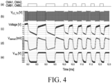
- FIG. 4 illustrates demodulation signals and signals transferred to a wireless power reception device through in-band communication according to control of switches corresponding to modulation capacitors in a wireless power reception device according to various embodiments.
- FIG. 4 may relate to a scenario in which the wireless power reception device 102 transmits an in-band communication signal based on the voltage V rec of the output end of the rectification circuit 225.
- (a) of FIG. 4 illustrates a control signal for controlling the plurality of first switches 231 and 232 and the plurality of second switches 233 and 234 output from the control circuit 250 when both of the plurality of first switches 231 and 232 and both of the plurality of second switches 233 and 234 are selected in the wireless power reception device 102 of FIG. 2 .
- (b) of FIG. 4 illustrates a voltage V LC_TX between both ends of the transmission coil 213.
- FIG. 4 illustrates an output signal at the output end 323 of the first low pass filter 320 of FIG. 3 .
- (d) of FIG. 4 illustrates an output signal V demod of the demodulation circuit 300.
- (e) of FIG. 4 illustrates a voltage Vrec at the output end of the rectification circuit 225 of the wireless power reception device 102.
- the wireless power reception device 102 may adjust the transmission power based on the output signal V demod .
- FIG. 5 is a flowchart illustrating operations performed in a wireless power reception device according to various embodiments.
- the control circuit 250 of the wireless power reception device e.g., the wireless power reception device 102 may identify the CEP value based on the output V rec of the rectification circuit 225 of the wireless power reception device 102 in operation 510.
- CEP_value V rec , target ⁇ V rec ScaledV rec , target ⁇ 128
- V rec, target may be the target voltage.
- ScaledV rec, target may be a predetermined constant.
- ScaledV rec, target may be a constant at which the absolute value of CEP _value is 1 when the difference between the output V rec of the rectification circuit 225 and the target voltage.
- the CEP value may have a value from - 127 to 127.
- the control circuit 250 of the wireless power reception device may select switches for modulating data to be transmitted to the wireless power transmission device from among the plurality of first switches 231 and 232 and the plurality of second switches 233 and 234, based on the CEP value.
- the control circuit 250 may select the first switch 232 connected to the first capacitor 262 having a smaller capacitance among the plurality of first capacitors 261 and 262 and the second switch 234 connected to the second capacitor 264 having a smaller capacitance among the plurality of second capacitors 263 and 264, select the first switch 231 connected to the first capacitor 261 having a larger capacitance among the plurality of first capacitors 261 and 262 and the second switch 233 connected to the second capacitor 263 having a larger capacitance among the plurality of second capacitors 263 and 264, or select both the first switches 231 and 232 and both the second switches 233 and 234.
- the control circuit 250 may select switches such that the capacitances of the modulation capacitors are small.
- the control circuit 250 may select switches such that the capacitances of the modulation capacitors are large.
- the rapid decrease in the CEP value may be a result of adjusting the transmission power based on the in-band signal by the wireless power reception device 102 due to smooth in-band communication.
- the control circuit 250 may select switches such that the capacitances of the modulation capacitors are small.
- the rate at which the CEP value decreases is slow or the CEP value does not decrease, the control circuit 250 may select the switches such that the capacitances of the modulation capacitors are small.
- the capacitances of the modulation capacitors may be larger when the first switch 231 and the second switch 233 are selected than when the first switch 232 and the second switch 234 are selected, and may be larger when both the first switches 231 and 233 and both the second switches 233 and 234 are selected than when the first switch 231 and the second switch 233 are selected.
- the wireless power reception device 102 may be equivalent to having a single capacitor having a capacitance of the sum of the capacitance C A1 of the first capacitor 261 and the capacitance C B1 of the first capacitor 262 and a single capacitor having a capacitance of the sum of the capacitance C A2 of the second capacitor 263 and the capacitance C B2 of the second capacitor 264 as modulation capacitors.
- FIGS. 6A and 6B An example of a reference for selecting switches in the control circuit 250 is described with reference to FIGS. 6A and 6B .
- the criteria described with reference to FIGS. 6A and 6B are exemplary, and the method for selecting the switches according to various embodiments is not limited as long as the switches are selected such that the capacitances of the modulation capacitors are small when in-band communication is smooth, and the capacitances of the modulation capacitors are large when in-band communication is not smooth.
- the control circuit 250 of the wireless power reception device may control the on/off of the selected switches based on the modulation of the data in operation 530.
- the modulated data may be data to be transmitted to the wireless power transmission device 101.
- the modulated data may indicate the voltage V rec of the output end of the rectification circuit 225.
- the modulated data may be a CEP value identified based on the voltage V rec of the output end of the rectification circuit 225.
- FIGS. 6A and 6B are flowcharts illustrating operations performed in a wireless power reception device according to various embodiments.
- FIGS. 6A and 6B illustrate operations that may be performed in a wireless power reception device including two first capacitors 261 and 262, two first switches 231 and 232, two second capacitors 263 and 264, and two second switches 233 and 234, like the wireless power reception device 102 illustrated in FIG. 2 .
- the wireless power reception device (e.g., the control circuit 250 of the wireless power reception device 102) may set the value of variable N for counting to 0 in operation 601.
- the wireless power reception device may identify the CEP value based on the output voltage V rec of the rectification circuit 225.
- the relationship between the output voltage V rec of the rectification circuit 225 and the CEP value has been described above with reference to Equation 1.
- the wireless power reception device e.g., the control circuit 250 of the wireless power reception device 102 may identify whether the absolute value of the CEP value is less than a predetermined first threshold.
- the wireless power reception device may select, in operation 611, the first switch 232 connected to the first capacitor 262 having a smaller capacitance of the two first switches 231 and 232 and the second switch 234 connected to the second capacitor 264 having a smaller capacitance of the two second switches 233 and 234.
- the wireless power reception device 102 is at a first level.
- the wireless power reception device e.g., the control circuit 250 of the wireless power reception device 102 may set the value of variable N for counting to 0.
- the wireless power reception device may transmit the CEP value to the wireless power transmission device using the selected switch and may wait for a predetermined period.
- the wireless power reception device e.g., the control circuit 250 of the wireless power reception device 102 may control the first switch 231 and the second switch 233 to be turned off, and may control the on/off of the first switch 232 and the second switch 234 to transmit an in-band communication signal indicating the CEP value.
- the wireless power reception device e.g., the control circuit 250 of the wireless power reception device 102 may return to operation 602.
- the wireless power reception device may increase the value of variable N for counting by 1 in operation 604.
- the wireless power reception device e.g., the control circuit 250 of the wireless power reception device 102 may identify whether the value of the variable N is larger than or equal to a predetermined first number of times.
- the wireless power reception device may select, in operation 621, the first switch 231 connected to the first capacitor 261 having a larger capacitance of the two first switches 231 and 232 and the second switch 233 connected to the second capacitor 263 having a larger capacitance of the two second switches 233 and 234.
- the wireless power reception device 102 is at a second level.
- the wireless power reception device may perform operation 613.
- the wireless power reception device e.g., the control circuit 250 of the wireless power reception device 102
- the wireless power transmission device 101 may control the transmitted wireless power such that the absolute value of the CEP value is close to zero.
- the wireless power reception device 102 may transition from the first level to the second level.
- the wireless power reception device e.g., the control circuit 250 of the wireless power reception device 102 may set the value of variable N to 0.
- the wireless power reception device may transmit the CEP value to the wireless power transmission device using the selected switch and may wait for a predetermined period.
- the wireless power reception device e.g., the control circuit 250 of the wireless power reception device 102
- the wireless power reception device may control the first switch 232 and the second switch 234 to be turned off, and may control the on/off of the first switch 231 and the second switch 233 to transmit an in-band communication signal indicating the CEP value in operation 623.
- the wireless power reception device when the wireless power reception device (e.g., the control circuit 250 of the wireless power reception device 102) is at the third level, the wireless power reception device (e.g., the control circuit 250 of the wireless power reception device 102) may control on/off of the first switch 231, the first switch 232, the second switch 233, and the second switch 234 to transmit the in-band communication signal indicating the CEP value in operation 623.
- the wireless power reception device (e.g., the control circuit 250 of the wireless power reception device 102) may identify the CEP value based on the output voltage V rec of the rectification circuit 225.
- the wireless power reception device e.g., the control circuit 250 of the wireless power reception device 102 may identify whether the absolute value of the CEP value identified in operation 624 exceeds the second threshold.
- the wireless power reception device e.g., the control circuit 250 of the wireless power reception device 102
- the wireless power reception device may set the value of variable N to 0 in operation 626, and may return to operation 602.
- the second threshold may be set to a value smaller than the first threshold.
- the wireless power reception device e.g., the control circuit 250 of the wireless power reception device 102
- the wireless power transmission device 101 may control the transmitted wireless power such that the absolute value of the CEP value is close to zero. Accordingly, when the absolute value of the CEP value decreases and becomes less than or equal to the second threshold, it may indicate that in-band communication is smoothly performed, and the wireless power reception device 102 may transition from the second level to the first level.
- the wireless power reception device e.g., the control circuit 250 of the wireless power reception device 102 may increase the value of variable N by 1 in operation 627.
- the wireless power reception device e.g., the control circuit 250 of the wireless power reception device 102 may identify whether the value of the variable N is larger than or equal to a predetermined second number of times.
- the wireless power reception device may select both the first switches 231 and 232 and both the second switches 233 and 234 in operation 631.
- the wireless power reception device 102 is at the third level.
- the wireless power reception device When it is identified that the value of variable N is less than the predetermined second number of times in operation 628, the wireless power reception device (e.g., the control circuit 250 of the wireless power reception device 102) may return to operation 623.
- the wireless power reception device e.g., the control circuit 250 of the wireless power reception device 102
- the number of times in which the absolute value of the CEP value is identified as exceeding the predetermined second threshold should be a predetermined second number of times.
- the wireless power transmission device 101 may control the transmitted wireless power such that the absolute value of the CEP value is close to zero. Accordingly, when the number of times in which the absolute value of the CEP value is identified as exceeding the predetermined second threshold becomes the predetermined second number of times, it may indicate that in-band communication is not smoothly performed, and the wireless power reception device 102 may transition from the second level to the third level.
- the wireless power reception device (e.g., the control circuit 250 of the wireless power reception device 102) having performed operation 631 may return to operation 623. If the absolute value of the CEP value decreases and becomes less than or equal to the second threshold when the wireless power reception device 102 is at the third level, the wireless power reception device 102 may transition to the first level. When the in-band communication is smoothly performed, the wireless power transmission device 101 may control the transmitted wireless power such that the absolute value of the CEP value is close to zero. Accordingly, when the absolute value of the CEP value decreases and becomes less than or equal to the second threshold, it may indicate that in-band communication is smoothly performed, and the wireless power reception device 102 may transition from the third level to the first level.
- FIG. 7 illustrates an example scenario of controlling a combination of capacitors for performing in-band communication in a wireless power reception device according to various embodiments.
- FIG. 7 illustrates a scenario in which wireless power is controlled by performing the operations illustrated in FIGS. 6A and 6B in the wireless power reception device (e.g., the control circuit 250 of the wireless power reception device 102), and the first threshold is 9, the second threshold is 3, the first number is 2, the second number is 4, and the target voltage is 10V.
- a control signal CMA1 applied from the control circuit 250 to the first switch 232 and a control signal CMA2 applied from the control circuit 250 to the second switch 234 are illustrated.
- a control signal CMB1 applied from the control circuit 250 to the first switch 231 and a control signal CMB2 applied from the control circuit 250 to the second switch 233 are illustrated.
- the signal indicated by CEP in FIG. 7 is a CEP value based on the voltage V rec of the output end of the rectification circuit 225 of the wireless power reception device 102, which is transferred from the wireless power reception device 102 to the wireless power transmitting device 101 in the form of an in-band communication signal.
- V demod denotes the output signal of the demodulation circuit 214.
- the wireless power reception device e.g., the control circuit 250 of the wireless power reception device 102 may perform operations 601 and 602, identify that the CEP value is -5 and the absolute value is less than 9, which is the first threshold, in operation 603, and perform operations 611 to 613. According to operation 613, the time immediately after a predetermined time elapses after transmitting the CEP value to the wireless power transmission device 101 may be t2.
- the first switch 231 and the second switch 233 may be controlled to be in the off state by the control signal CMB1 and the control signal CMB2, and the first switch 232 and the second switch 234 may be controlled to repeat the on/off state by the control signal CMA1 and the control signal CMA2.
- the wireless power reception device 102 may be at the first level.
- the wireless power reception device (e.g., the control circuit 250 of the wireless power reception device 102) may perform operation 602, identify that the CEP value is -7 and the absolute value is less than 9, which is the first threshold, in operation 603, and perform operations 611 to 613. According to operation 613, the time immediately after a predetermined time elapses after transmitting the CEP value to the wireless power transmission device 101 may be t3. From t2 to t3, the wireless power reception device 102 may be at the first level.
- the wireless power reception device may perform operation 602, identify that the CEP value is -10 and the absolute value is not less than 9, which is the first threshold, in operation 603, and increase N from 0 to 1 in operation 604. In operation 605, it may be identified that 1 which is the value of N is less than 2 which is the first number of times, and operation 613 may be performed. Since the switch selected in operation 611 between t2 and t3 is not changed, the wireless power reception device 102 may be at the first level when performing operation 613. According to operation 613, the time immediately after a predetermined time elapses after transmitting the CEP value to the wireless power transmission device 101 may be t4.
- the wireless power reception device may perform operation 602, identify that the CEP value is -10 and the absolute value is not less than 9, which is the first threshold, in operation 603, and increase N from 1 to 2 in operation 604.
- operation 605 it may be identified that 2 which is the value of N is equal to 2 which is the first number of times, and operation 621 may be performed.
- the first switch 232 and the second switch 234 may be controlled to be in the off state by the control signal CMA1 and the control signal CMA2, and the first switch 231 and the second switch 233 may be controlled to repeat the on/off state by the control signal CMB1 and the control signal CMB2.
- the wireless power reception device 102 may be at the second level.
- the wireless power reception device 102 may perform operations 622 and 623.
- operation 623 the CEP value transmitted to the wireless power transmission device 101 may be -10.
- the amplitude of the in-band communication signal transmitted from the wireless power reception device 102 to the wireless power transmission device 101 in operation 623 may be sufficiently large.
- the voltage V rec at the output end of the rectification circuit 225 may be close to the target voltage of 10V, and the CEP value identified when the wireless power reception device 102 performs operation 624 may be -4.
- operation 625 it may be identified that 4 which is the absolute value of the CEP value is larger than 3 which is the second threshold, and the wireless power reception device 102 may change the value of N from 0 to 1 in operation 627, identify that 1 which is the value of N is less than 3 which is the second number of times in operation 628, and may perform operation 623.
- the CEP value transmitted when the wireless power reception device 102 performs operation 623 may be -4.
- the voltage Vrec at the output end of the rectification circuit 225 may be close to the target voltage of 10V, and the CEP value identified when the wireless power reception device 102 performs operation 624 may be -3.
- the wireless power reception device 102 may identify that 3, which is the absolute value of the CEP value, is equal to or less than 3, which is the second threshold, and in operation 626, the wireless power reception device 102 may set the value of N to 0.
- the wireless power reception device 102 may perform operation 611. In other words, the wireless power reception device 102 may transition from the second level to the first level at t5.
- FIG. 8 illustrates an example scenario of controlling a combination of capacitors for performing in-band communication in a wireless power reception device according to various embodiments.
- FIG. 7 illustrates a scenario in which wireless power is controlled by performing the operations illustrated in FIGS. 6A and 6B in the wireless power reception device (e.g., the control circuit 250 of the wireless power reception device 102), and the first threshold is 9, the second threshold is 3, the first number is 3, the second number is 2, and the target voltage is 10V.
- the wireless power reception device may perform operations 601 and 602, identify that the CEP value is -6 and the absolute value is less than 9, which is the first threshold, in operation 603, and perform operations 611 to 613.
- the CEP value transmitted in operation 613 may be -6.
- the wireless power reception device 102 may be at the first level.
- the CEP value is repeatedly transmitted to the wireless power transmission device 101 in the form of an in-band communication signal at the first level, the difference between the voltage V rec at the output end of the rectification circuit 225 and the target voltage may increase.
- the absolute value of the CEP exceeds the first threshold of 9, and accordingly, the wireless power reception device 102 may transition from the first level to the second level at t2.
- the CEP value is repeatedly transmitted to the wireless power transmission device 101 in the form of an in-band communication signal at the second level, the difference between the voltage V rec at the output end of the rectification circuit 225 and the target voltage may not be reduced.
- N may be equal to 2 which is the second number of times. Accordingly, the wireless power reception device 102 may transition from the second level to the third level according to operation 631 at t3.
- the first switch 231, the first switch 232, the second switch 233, and the second switch 234 may be controlled to repeat the on/off state.
- the wireless power reception device 102 at the third level may repeat operation 623, operation 624, operation 625, operation 627, operation 628, and operation 631 until the absolute value of the CEP value decreases below the second threshold.
- the absolute value of the CEP value may be reduced to be less than or equal to the second threshold, and the wireless power reception device 102 may transition from the third level to the first level at t4.
- FIG. 9 is a view illustrating a configuration of a wireless power reception device according to various embodiments.
- a wireless power reception device 900 may include a resonance circuit 910, a rectification circuit 920, a plurality of first capacitors C A1 , C B1 , and C C1 , a plurality of first switches S A1 , S B1 , and S C1 respectively connecting the plurality of first capacitors and a ground, a plurality of second capacitors C A2 , C B2 , and C C2 , a plurality of second switches S A2 , S B2 , and S C2 respectively connecting the plurality of second capacitors and the ground, a control circuit 930, a capacitor 941, a regulator 942, a capacitor 943, a charger 944, and a battery 945.
- the wireless power reception device 102 includes two first capacitors 261 and 262, two first switches 231 and 232, two second capacitors 263 and 264, and two second switches 233 and 234, whereas the wireless power reception device 900 includes three first capacitors C A1 , C B1 , and C C1 , three first switches S A1 , S B1 , and S C1 , three second capacitors C A2 , C B2 , and C C2 , and three second switches S A2 , S B2 , and S C2 .
- the details of the resonance circuit 220, the rectification circuit 225, the control circuit 250, the capacitor 641, the regulator 242, the capacitor 643, the charger 244, and the battery 245 described above with reference to FIG. 2 may be equally applied to the resonance circuit 910, the rectification circuit 920, the control circuit 930, the capacitor 941, the regulator 942, the capacitor 943, the charger 944, and the battery 945, respectively.
- the control circuit 930 may select switches for modulating data to be transmitted to the wireless power transmission device (not shown) from among the plurality of first switches S A1 , S B1 , S C1 and the plurality of second switches S A2 , S B2 , and S C2 based on the voltage Vrec at the output end of the rectification circuit 920. According to various embodiments, the control circuit 930 may select the switches based on the CEP value identified based on the voltage V rec at the output end of the rectification circuit 920.
- a combination of capacitors that may be used as a modulation capacitor among the plurality of first capacitors C A1 , C B1 , and C C1 and the plurality of second capacitors C A2 , C B2 , and C C2 may vary. While the wireless power reception device 102 illustrated in FIG. 2 may be at the first level, the second level, and the third level, the wireless power reception device 900 illustrated in FIG. 9 may be at up to seven levels.
- the levels that the wireless power reception device 900 may have are arranged in the order of the capacitances of the modulation capacitors as follows.
- the control circuit 930 may select switches such that the capacitances of the modulation capacitors are small. For example, in response to identifying that the CEP value identified based on the voltage V rec of the output end of the rectification circuit 920 is less than a first threshold, the control circuit 930 may select the first switch S A1 connected to the first capacitor C A1 having the smallest capacitance among the plurality of first switches S A1 , S B1 , and Sci and the second switch S A2 connected to the second capacitor C A2 having the smallest capacitance among the plurality of second switches S A2 , S B2 , and S C2 as switches for modulating data.
- the wireless power reception device 900 may be at the first level.
- the control circuit 930 may select the first switch S A1 connected to the first capacitor C A1 having the smallest capacitance among the plurality of first switches S A1 , S B1 , and Sci, and the second switch S A2 connected to the second capacitor C A2 having the smallest capacitance among the plurality of second switches S A2 , S B2 , and S C2 as switches for modulating data.
- the wireless power reception device 900 may transition to the first level.
- control circuit 930 may select switches such that the capacitances of the modulation capacitors are large.
- FIG. 9 illustrates that the wireless power reception device 900 includes three first capacitors C A1 , C B1 , and C C1 , three first switches S A1 , S B1 , and S C1 , three second capacitors C A2 , C B2 , and C C2 , and three second switches S A2 , S B2 , and S C2 .
- the numbers of first capacitors, first switches, second capacitors, and second switches that the wireless power reception device 102 may include are not limited.
- a wireless power reception device may comprise a resonance circuit (e.g., the resonance circuit 220) configured to receive wireless power from a wireless power transmission device (e.g., the wireless power transmission device 101), a plurality of first capacitors (e.g., the plurality of first capacitors 261 and 262), a plurality of first switches (e.g., the plurality of first switches 231 and 232), a plurality of second capacitors (e.g., the plurality of second capacitors 263 and 264), a plurality of second switches (e.g., the plurality of second switches 233 and 234), a rectification circuit (e.g., the rectification circuit 225) connected to a first end and a second end of the resonance circuit 220, and a control circuit (e.g., the control circuit 250) connected to the rectification circuit 225.
- a resonance circuit e.g., the resonance circuit 220
- Each of first ends of the plurality of first capacitors 261 and 262 may be connected to the first end of the resonance circuit 220, second ends of the plurality of first capacitors 261 and 262 may be respectively connected to first ends of the plurality of first switches 231 and 232, and second ends of the plurality of first switches 231 and 232 may be connected to a ground.
- Each of first ends of the plurality of second capacitors 263 and 264 may be connected to the second end of the resonance circuit 220, second ends of the plurality of second capacitors 263 and 264 may be respectively connected to first ends of the plurality of second switches 233 and 234, and second ends of the plurality of second switches 233 and 234 may be connected to the ground.
- the control circuit 250 may be configured to select switches for modulating data to be transmitted to the wireless power transmission device 101 among the plurality of first switches 231 and 232 and the plurality of second switches 233 and 234 based on a CEP value identified based on an output of the rectification circuit 225 and control on/off of the selected switches based on modulation of the data.
- control circuit 250 may be configured to wait for a predetermined period after controlling the on/off of the selected switches based on the modulation of the data and re-identify the CEP value after the predetermined period elapses.
- the plurality of first capacitors 261 and 262 may include two first capacitors 261 and 262.
- the plurality of second capacitors 263 and 264 may include two second capacitors 263 and 264, and the plurality of first switches 231 and 232 may include two first switches 231 and 232.
- the plurality of second switches 233 and 234 may include two second switches 233 and 234.
- the control circuit 250 may be configured to, when selecting switches for modulating the data from among the plurality of first switches 231 and 232 and the plurality of second switches 233 and 234, select a first switch (e.g., the first switch 232) connected to a capacitor (e.g., the first capacitor 262) having a smaller capacitance of the two first switches and a second switch (e.g., the second switch 234) connected to a capacitor (e.g., the second capacitor 264) having a smaller capacitance of the two second switches, select a first switch (e.g., the first switch 231) connected to a capacitor (e.g., the first capacitor 261) having a larger capacitance of the two first switches 231 and 232 and a second switch (e.g., the second switch 233) connected to a capacitor (e.g., the second capacitor 263) having a larger capacitance of the two second switches 233 and 234, or select all of the two first switches 231 and 232 and the two second switches 233 and 234.
- control circuit 250 may be configured to select the first switch 232 connected to the capacitor (e.g., the first capacitor 262) having the smaller capacitance of the two first switches 231 and 232 and the second switch 234 connected to the capacitor (e.g., the second capacitor 264) having the smaller capacitance of the two second switches 233 and 234, as the switches for modulating the data, in response to identifying that an absolute value of the CEP value is smaller than a first threshold.
- control circuit 250 may be configured to select the first switch 231 connected to the capacitor (e.g., the first capacitor 261) having the larger capacitance of the two first switches 231 and 232 and the second switch 233 connected to the capacitor (e.g., the second capacitor 263) having the larger capacitance of the two second switches 233 and 234, as the switches for modulating the data, in response to a number of times in which the absolute value of the CEP value is identified as the first threshold or more being a first number or more.
- the control circuit 250 may be configured to, in response to identifying that the absolute value of the CEP value is a second threshold or less in a state in which the first switch 231 connected to the capacitor (e.g., the first capacitor 261) having the larger capacitance of the two first switches 231 and 232 and the second switch 233 connected to the capacitance (e.g., the second capacitor 263) having the larger capacitance of the two second switches 233 and 234 are selected as the switches for modulating the data, select the first switch 232 connected to the capacitor (e.g., the first capacitor 262) having the smaller capacitance of the two first switches 231 and 232 and the second switch 234 connected to the capacitor (e.g., the second capacitor 264) having the smaller capacitance of the two second switches 233 and 234, as the switches for modulating the data.
- the first switch 231 connected to the capacitor e.g., the first capacitor 261 having the larger capacitance of the two first switches 231 and 232 and the second switch 233 connected to the capacit
- control circuit 250 may be configured to, in response to identifying that a number of times in which the absolute value of the CEP value is identified as a second threshold or more is a second number or more in a state in which the first switch 231 connected to the capacitor (e.g., the first capacitor 261) having the larger capacitance of the two first switches 231 and 232 and the second switch 233 connected to the capacitor (e.g., the second capacitor 263) having the larger capacitance of the two second switches 233 and 234 are selected as the switches for modulating the data, select all of the two first switches 231 and 232 and the two second switches 233 and 234 as the switches for modulating the data.
- the first switch 231 connected to the capacitor e.g., the first capacitor 261 having the larger capacitance of the two first switches 231 and 232 and the second switch 233 connected to the capacitor (e.g., the second capacitor 263) having the larger capacitance of the two second switches 233 and 234 are selected as the switches for modulating the data
- control circuit 250 may be configured to, in response to identifying that the absolute value of the CEP value is less than the second threshold in a state where both all of the two first switches 231 and 232 and the two second switches 233 and 234 are selected as the switches for modulating the data, select the first switch 232 connected to the capacitor (e.g., the first capacitor 262) having the smaller capacitance of the two first switches 231 and 232 and the second switch 234 connected to the capacitor (e.g., the second capacitor 264) having the smaller capacitance of the two second switches 233 and 234, as the switches for modulating the data.
- the capacitor e.g., the first capacitor 262
- the second switch 234 connected to the capacitor having the smaller capacitance of the two second switches 233 and 234, as the switches for modulating the data.
- control circuit 250 may be configured to, in response to identifying that the CEP value is less than a first threshold, select a first switch connected to a capacitor having a smallest capacitance among the plurality of first switches 231 and 232 and a second switch connected to a capacitor having a smallest capacitance among the plurality of second switches 233 and 234, as the switches for modulating the data.
- control circuit 250 may be configured to, in response to identifying that the CEP value is less than a second threshold in a state in which the selected switches differ from a combination of a first switch connected to a capacitor having a smallest capacitance among the plurality of first switches 231 and 232 and a second switch connected to a capacitor having a smallest capacitance among the plurality of second switches 233 and 234, select a first switch connected to a capacitor having a smallest capacitance among the plurality of first switches 231 and 232 and a second switch connected to a capacitor having a smallest capacitance among the plurality of second switches 233 and 234, as the switches for modulating the data.
- the modulated data may indicate the CEP value.
- a method performed by a wireless power reception device including a resonance circuit (e.g., the resonance circuit 220), a plurality of first capacitors (e.g., the plurality of first capacitors 261 and 262), a plurality of first switches (e.g., the plurality of first switches 231 and 232), a plurality of second capacitors (e.g., the plurality of second capacitors 263 and 264), and a plurality of second switches (e.g., the plurality of second switches 233 and 234), wherein each of first ends of the plurality of first capacitors 261 and 262 may be connected to the first end of the resonance circuit 220, second ends of the plurality of first capacitors 261 and 262 are respectively connected to first ends of the plurality of first switches 231 and 232, and second ends of the plurality of first switches 231 and 232 are connected to a ground, wherein each of first ends of the plurality of second capacitors
- the method may further comprise waiting for a predetermined period after controlling the on/off of the selected switches based on the modulation of the data, and re-identifying the CEP value after the predetermined period elapses.
- the plurality of first capacitors 261 and 262 may include two first capacitors 261 and 262.
- the plurality of second capacitors 263 and 264 may include two second capacitors 263 and 264.
- the plurality of first switches 231 and 232 may include two first switches 231 and 232.
- the plurality of second switches 233 and 234 may include two second switches 233 and 234.
- Selecting the switches for modulating the data may include one of selecting a first switch 232 connected to a capacitor (e.g., the first capacitor 262) having a smaller capacitance of the two first switches 231 and 232 and a second switch 234 connected to a capacitor (e.g., the second capacitor 264) having a smaller capacitance of the two second switches 233 and 234, selecting a first switch 231 connected to a capacitor (e.g., the first capacitor 261) having a larger capacitance of the two first switches 231 and 232 and a second switch 233 connected to a capacitor (e.g., the second capacitor 263) having a larger capacitance of the two second switches 233 and 234, or selecting all of the two first switches 231 and 232 and the two second switches 233 and 234.
- Selecting the switches for modulating the data may include selecting the first switch 232 connected to the capacitor (e.g., the first capacitor 262) having the smaller capacitance of the two first switches 231 and 232 and the second switch 234 connected to the capacitor (e.g., the second capacitor 264) having the smaller capacitance of the two second switches 233 and 234, as the switches for modulating the data, in response to identifying that an absolute value of the CEP value is smaller than a first threshold.
- selecting the switches for modulating the data may include selecting the first switch 231 connected to the capacitor (e.g., the first capacitor 261) having the larger capacitance of the two first switches 231 and 232 and the second switch 233 connected to the capacitor (e.g., the second capacitor 263) having the larger capacitance of the two second switches 233 and 234, as the switches for modulating the data, in response to a number of times in which the absolute value of the CEP value is identified as the first threshold or more being a first number or more.
- the method may further comprise, in response to identifying that the absolute value of the CEP value is a second threshold or less in a state in which the first switch 231 connected to the capacitor (e.g., the first capacitor 261) having the larger capacitance of the two first switches 231 and 232 and the second switch 233 connected to the capacitance (e.g., the second capacitor 263) having the larger capacitance of the two second switches 233 and 234 are selected as the switches for modulating the data, selecting the first switch 232 connected to the capacitor (e.g., the first capacitor 262) having the smaller capacitance of the two first switches 231 and 232 and the second switch 234 connected to the capacitor (e.g., the second capacitor 264) having the smaller capacitance of the two second switches 233 and 234, as the switches for modulating the data and, based on the modulation of the data indicating the CEP value, controlling on/off of a first switch 232 connected to a capacitor (e.g., the first capacitor 262) having a
- the method may further comprise, in response to identifying that a number of times in which the absolute value of the CEP value is identified as a second threshold or more is a second number or more in a state in which the first switch 231 connected to the capacitor (e.g., the first capacitor 261) having the larger capacitance of the two first switches 231 and 232 and the second switch 233 connected to the capacitor (e.g., the second capacitor 263) having the larger capacitance of the two second switches 233 and 234 are selected as the switches for modulating the data, selecting all of the two first switches 231 and 232 and the two second switches 233 and 234 as the switches for modulating the data and, based on the modulation of the data indicating the CEP value, controlling on/off of all of the two first switches 231 and 232 and the two second switches 233 and 234.
- the first switch 231 connected to the capacitor e.g., the first capacitor 261 having the larger capacitance of the two first switches 231 and 232 and the second switch 233 connected to the
- the method may further comprise, in response to identifying that the absolute value of the CEP value is less than the second threshold in a state in which all of the two first switches 231 and 232 and the two second switches 233 and 234 are selected as the switches for modulating the data, selecting the first switch 232 connected to the capacitor (e.g., the first capacitor 262) having the smaller capacitance of the two first switches 231 and 232 and the second switch 234 connected to the capacitor (e.g., the second capacitor 264) having the smaller capacitance of the two second switches 233 and 234, as the switches for modulating the data and, based on the modulation of the data indicating the CEP value, controlling on/off of a first switch 232 connected to a capacitor (e.g., the first capacitor 262) having a smaller capacitance of the two first switches 231 and 232 and a second switch 234 connected to a capacitor (e.g., the second capacitor 264) having a smaller capacitance of the two second switches 233 and 234.
- selecting the switches for modulating the data may include, in response to identifying that the absolute value of the CEP value is less than a first threshold, selecting a first switch connected to a capacitor having a smallest capacitance among the plurality of first switches 231 and 232 and a second switch connected to a capacitor having a smallest capacitance among the plurality of second switches 233 and 234, as the switches for modulating the data.
- the wireless power reception device and the wireless power transmission device may be various types of devices.
- the wireless power reception device and the wireless power transmission device may include, for example, a portable communication device (e.g., a smartphone), a computer device, a portable multimedia device, a portable medical device, a camera, a wearable device, or a home appliance.
- a portable communication device e.g., a smartphone
- a computer device e.g., a computer device
- a portable multimedia device e.g., a portable medical device
- a camera e.g., a portable medical device
- a wearable device e.g., a portable medical device
- each of such phrases as “A or B,” “at least one of A and B,” “at least one of A or B,” “A, B, or C,” “at least one of A, B, and C,” and “at least one of A, B, or C,” may include all possible combinations of the items enumerated together in a corresponding one of the phrases.
- such terms as “1st” and “2nd,” or “first” and “second” may be used to simply distinguish a corresponding component from another, and does not limit the components in other aspect (e.g., importance or order).
- an element e.g., a first element
- the element may be coupled with the other element directly (e.g., wiredly), wirelessly, or via a third element.
- module may include a unit implemented in hardware, software, or firmware, and may interchangeably be used with other terms, for example, “logic,” “logic block,” “part,” or “circuitry”.
- a module may be a single integral component, or a minimum unit or part thereof, adapted to perform one or more functions.
- the module may be implemented in a form of an application-specific integrated circuit (ASIC).
- ASIC application-specific integrated circuit
- Various embodiments as set forth herein may be implemented as software (e.g., the program 140) including one or more instructions that are stored in a storage medium (e.g., internal memory 136 or external memory 138) that is readable by a machine (e.g., the electronic device 101).
- a processor e.g., the processor 120
- the machine e.g., the electronic device 101
- the one or more instructions may include a code generated by a complier or a code executable by an interpreter.
- the storage medium readable by the machine may be provided in the form of a non-transitory storage medium.
- the term “non-transitory” simply means that the storage medium is a tangible device, and does not include a signal (e.g., an electromagnetic wave), but this term does not differentiate between where data is semi-permanently stored in the storage medium and where the data is temporarily stored in the storage medium.
- a method may be included and provided in a computer program product.
- the computer program products may be traded as commodities between sellers and buyers.
- the computer program product may be distributed in the form of a machine-readable storage medium (e.g., compact disc read only memory (CD-ROM)), or be distributed (e.g., downloaded or uploaded) online via an application store (e.g., Play Store TM ), or between two user devices (e.g., smartphones) directly. If distributed online, at least part of the computer program product may be temporarily generated or at least temporarily stored in the machine-readable storage medium, such as memory of the manufacturer's server, a server of the application store, or a relay server.
- CD-ROM compact disc read only memory
- an application store e.g., Play Store TM
- two user devices e.g., smartphones
- each component e.g., a module or a program of the above-described components may include a single entity or multiple entities. Some of the plurality of entities may be separately disposed in different components. According to various embodiments, one or more of the above-described components may be omitted, or one or more other components may be added. Alternatively or additionally, a plurality of components (e.g., modules or programs) may be integrated into a single component. In such a case, according to various embodiments, the integrated component may still perform one or more functions of each of the plurality of components in the same or similar manner as they are performed by a corresponding one of the plurality of components before the integration.
- operations performed by the module, the program, or another component may be carried out sequentially, in parallel, repeatedly, or heuristically, or one or more of the operations may be executed in a different order or omitted, or one or more other operations may be added.
Landscapes
- Engineering & Computer Science (AREA)
- Computer Networks & Wireless Communication (AREA)
- Power Engineering (AREA)
- Signal Processing (AREA)
- Near-Field Transmission Systems (AREA)
- Charge And Discharge Circuits For Batteries Or The Like (AREA)
Abstract
Description
- Various embodiments relate to a wireless power reception device performing in-band communication with a wireless power transmission device and a method for performing in-band communication in a wireless power reception device.
- The wireless power transmission technology using the magnetic induction scheme is a scheme for transferring power by the electromagnetic field induced in the coil. The wireless power transmitting device applies a current to the transmission coil to generate an electromagnetic field, and an induced current is formed in the reception coil of the wireless power receiving device, so that power may be wirelessly transmitted. Wireless power transmission technology may contribute to convenience in that there is no need to connect the charging terminals to the electronic device.
- When receiving wireless power from the wireless power transmission device, the wireless power reception device may transmit a signal to the wireless power transmission device through in-band communication to control the received wireless power. An additional resonance element may be connected to the resonance circuit of the wireless power reception device and, as the additional resonance element is connected, the current flowing through the transmission coil of the wireless power transmission device and/or the voltage across the transmission coil may change. The wireless power transmission device may obtain the signal by performing demodulation on the current flowing through the transmission coil and/or the voltage across the transmission coil. The process of changing the current flowing through the transmission coil of the wireless power transmission device and/or the voltage across the transmission coil by controlling the connection between the resonance circuit and the additional resonance element in the wireless power reception device may be referred to as a process of transmitting an in-band communication signal to the wireless power transmission device. The wireless power transmission device may control wireless power transmitted to the wireless power reception device based on the signal obtained from the wireless power reception device through in-band communication.
- One or more modulation capacitors for performing in-band communication may be connected to the resonance circuit of the wireless power reception device. When the capacitance of the modulation capacitor is large, the current flowing through the transmission coil of the wireless power transmission device and/or the voltage across the transmission coil may be greatly changed. In other words, when the capacitance of the modulation capacitor is large, a signal having a large amplitude may be transferred to the wireless power transmission device. However, when the capacitance of the modulation capacitor is large, overshoot of the voltage output from the rectification circuit of the wireless power reception device increases, resulting in increased voltage stress in the rectification circuit and increased loss in the regulator. Further, audible noise may occur as perturbation of the audible frequency band periodically occurs in the in-band signal.
- Due to the non-linear characteristics of the resonance system, even when the capacitance of the modulation capacitor is the same, the amplitude of the demodulation signal that may be obtained by performing demodulation on the current flowing through the transmission coil and/or the voltage across the transmission coil in the wireless power transmission device may vary depending on the load conditions and the switching frequency.
- The wireless power reception device according to various embodiments may include a plurality of capacitors connected to the resonance circuit and may select a combination of modulation capacitors based on the control error packet (CEP) value identified based on the output of the resonance circuit.
- According to various embodiments, a wireless power reception device may comprise a resonance circuit configured to receive wireless power from a wireless power transmission device, a plurality of first capacitors, a plurality of first switches, a plurality of second capacitors, a plurality of second switches, a rectification circuit connected to a first end and a second end of the resonance circuit, and a control circuit connected to the rectification circuit. Each of first ends of the plurality of first capacitors may be connected to the first end of the resonance circuit, second ends of the plurality of first capacitors may be respectively connected to first ends of the plurality of first switches, and second ends of the plurality of first switches may be connected to a ground. Each of first ends of the plurality of second capacitors may be connected to the second end of the resonance circuit, second ends of the plurality of second capacitors may be respectively connected to first ends of the plurality of second switches, and second ends of the plurality of second switches may be connected to the ground. The control circuit may be configured to select switches for modulating data to be transmitted to the wireless power transmission device among the plurality of first switches and the plurality of second switches based on a CEP value identified based on an output of the rectification circuit and control on/off of the selected switches based on modulation of the data.
- According to various embodiments, a method performed by a wireless power reception device including a resonance circuit, a plurality of first capacitors, a plurality of first switches, a plurality of second capacitors, and a plurality of second switches, wherein each of first ends of the plurality of first capacitors is connected to the first end of the resonance circuit, second ends of the plurality of first capacitors are respectively connected to first ends of the plurality of first switches, and second ends of the plurality of first switches are connected to a ground, wherein each of first ends of the plurality of second capacitors is connected to the second end of the resonance circuit, second ends of the plurality of second capacitors are respectively connected to first ends of the plurality of second switches, and second ends of the plurality of second switches are connected to the ground, may comprise identifying a CEP value based on an output of a rectification circuit of the wireless power reception device, selecting switches for modulating data to be transmitted to a wireless power transmission device among the plurality of first switches and the plurality of second switches based on the CEP value, and controlling on/off of the selected switches based on the modulation of the data.
- According to various embodiments, there may be provided a wireless power reception device performing in-band communication with a wireless power transmission device and a method for performing in-band communication in a wireless power reception device. The wireless power reception device according to various embodiments may include a plurality of capacitors connected to the resonance circuit and may select a combination of modulation capacitors based on the CEP value identified based on the output of the resonance circuit. The wireless power reception device according to various embodiments may determine whether wireless power is properly controlled through in-band communication based on the CEP value and, accordingly, adaptively select a combination of modulation capacitors. Therefore, the wireless power reception device according to various embodiments may maintain the minimum capacitance of the modulation capacitors within a range in which smooth in-band communication is possible, making it possible to minimize the voltage stress of the resonance circuit and the loss in the regulator and properly control wireless power while mitigating audible noise.
-
-
FIG. 1 is a block diagram illustrating a wireless power transmission device and a wireless power receiving device according to various embodiments; -
FIG. 2 is a view illustrating a configuration of a wireless power transmission device and a wireless power reception device according to various embodiments; -
FIG. 3 is a view illustrating a demodulation circuit of a wireless power transmission device according to various embodiments; -
FIG. 4 illustrates demodulation signals and signals transferred to a wireless power reception device through in-band communication according to control of switches corresponding to a modulation capacitor in a wireless power reception device according to various embodiments; -
FIG. 5 is a flowchart illustrating operations performed in a wireless power reception device according to various embodiments; -
FIGS. 6A and6B are flowcharts illustrating operations performed in a wireless power reception device according to various embodiments; -
FIG. 7 illustrates an example scenario of controlling a combination of capacitors for performing in-band communication in a wireless power reception device according to various embodiments; -
FIG. 8 illustrates an example scenario of controlling a combination of capacitors for performing in-band communication in a wireless power reception device according to various embodiments; and -
FIG. 9 is a view illustrating a configuration of a wireless power reception device according to various embodiments. -
FIG. 1 is a block diagram illustrating a wireless power transmission device and a wireless power receiving device according to various embodiments. - Referring to
FIG. 1 , a wirelesspower transmission device 101 according to various embodiments may transmit wireless power to a wirelesspower reception device 102. According to various embodiments, the wirelesspower transmission device 101 may transmit wireless power to the wirelesspower reception device 102 according to an induction scheme. When the wirelesspower transmission device 101 transmits wireless power to the wirelesspower reception device 102 by the induction scheme, the wirelesspower transmitting device 101 may include at least one of, e.g., a power source, a direct current (DC)-alternating current (AC) converting circuit, an amplifying circuit, an impedance matching circuit, at least one capacitor, at least one coil, and a communication modulation/demodulation circuit. The at least one capacitor together with the at least one coil may constitute a resonance circuit. Thewireless power transmitter 101 may be implemented in a scheme defined in the wireless power consortium (WPC) standards (or Qi standards). - According to various embodiments, the wireless
power transmission device 101 may include a transmission coil for transmitting wireless power. As current is applied to the transmission coil, the transmission coil may generate an induced magnetic field. The wirelesspower reception device 102 may include a reception coil for receiving wireless power. According to the change in the induced magnetic field generated by the transmission coil, an induced current may flow between two opposite ends of the reception coil. The process of generating an induced magnetic field by the wirelesspower transmission device 101 may be represented as transmitting wireless power to the wirelesspower reception device 102 by the wirelesspower transmission device 101. The process in which the induced current is rendered to flow between two opposite ends of the wirelesspower reception device 102 according to the change in the induced magnetic field generated by the wirelesspower transmission device 101 may be represented as receiving wireless power from the wirelesspower transmission device 101 by the wirelesspower reception device 102. - According to various embodiments, the wireless
power reception device 102 may transmit an in-band communication signal to the wirelesspower transmission device 101. The wirelesspower reception device 102 may transmit a signal indicating information related to wireless power received from the wirelesspower transmission device 101 to the wirelesspower reception device 102 using in-band communication. According to various embodiments, the in-band communication signal may indicate a value based on a difference between an output voltage of the rectifier circuit of the wirelesspower reception device 102 and a target voltage. The in-band communication signal may indicate, e.g., a control error packet (CEP) value based on a difference between an output voltage of the rectification circuit of the wirelesspower reception device 102 and the target voltage. - The wireless
power transmission device 101 may control wireless power transmitted to the wirelesspower reception device 102 based on the in-band communication signal. According to various embodiments, the wirelesspower transmission device 101 may control wireless power by controlling a switching frequency and/or a pulse width modulation (PWM) duty cycle. - According to an embodiment, the wireless
power reception device 102 may select a combination of modulation capacitors to be used to transmit the in-band communication signal based on the wireless power received from the wirelesspower transmission device 101. According to various embodiments, the wirelesspower reception device 102 may select a combination of modulation capacitors to be used to transmit an in-band communication signal, based on a CEP value. As combinations of modulation capacitors having different capacitances are used to transmit the in-band communication signal, the amplitude of the in-band communication signal may vary. -
FIG. 2 is a view illustrating a configuration of a wireless power transmission device and a wireless power reception device according to various embodiments. - Referring to
FIG. 2 , a wirelesspower transmission device 101 may include apower source 211, a plurality of switches Q1, Q2, Q3, and Q4, acapacitor 212, atransmission coil 213, ademodulation circuit 214, and acontrol circuit 215. - According to various embodiments, the DC power provided by the
power source 211 may be converted into the AC power by the plurality of switches Q1, Q2, Q3, and Q4 constituting a full bridge circuit. One end of thetransmission coil 213 may be connected to a connection point between the switches Q1 and Q2 through thecapacitor 212, and the other end of thetransmission coil 213 may be connected to the connection point between the switches Q3 and Q4. Thecontrol circuit 215 may control on/off states of the plurality of switches Q1, Q2, Q3, and Q4 such that DC power provided by thepower source 211 may be converted into AC power. - The AC power converted by the plurality of switches Q1, Q2, Q3, and Q4 may be applied to the
transmission coil 213. Thetransmission coil 213 may form a magnetic field based on the applied AC power. Part of the magnetic field formed by thetransmission coil 213 may pass through the cross section of thereception coil 221 of the wirelesspower receiving device 102. As the magnetic field passing through the cross section of thereception coil 221 is changed over time, an induced current may flow through thereception coil 221. - According to various embodiments, the
demodulation circuit 214 may demodulate the voltage VLC_TX across thetransmission coil 213 to output the demodulation signal Vdemod. An example of the configuration of thedemodulation circuit 214 is described below with reference toFIG. 3 . - According to various embodiments, the
control circuit 215 may control the wireless power transmitted to the wirelesspower reception device 102 by controlling the frequency at which the on/off state of the plurality of switches Q1, Q2, Q3, and Q4 is switched based on the demodulation signal Vdemod output by thedemodulation circuit 214. According to various embodiments, thecontrol circuit 215 may control the wireless power by controlling the PWM duty cycle based on the demodulation signal Vdemod. - According to various embodiments, the wireless
power reception device 102 may include aresonance circuit 220, arectification circuit 225, acontrol circuit 250, a plurality offirst capacitors first switches second capacitors second switches capacitor 241, aregulator 242, acapacitor 243, acharger 244, and abattery 245. - According to various embodiments, the
resonance circuit 220 may include areception coil 221, acapacitor 222, and acapacitor 223. One end of thecapacitor 222 may be connected to thereception coil 221, and the other end of thecapacitor 222 may be connected to one end of thecapacitor 223 and one end of therectification circuit 225. One end of thecapacitor 223 may be connected to the other end of thecapacitor 222, and the other end of thecapacitor 223 may be connected to the other end of thereception coil 221. In other words, thecapacitor 223 may be connected in parallel to a circuit formed by connecting thereception coil 221 and thecapacitor 222 in series. The other end of thecapacitor 223 may be connected to the other end of therectification circuit 225. - According to various embodiments, the
rectification circuit 225 may include a plurality of switches S1, S2, S3, and S4 constituting the full bridge circuit. One end of theresonance circuit 220 may be connected to a connection point between the switches S1 and S2, and the other end of theresonance circuit 220 may be connected to the connection point between the switches S3 and S4. Therectification circuit 225 may convert the AC-type wireless power received through theresonance circuit 220 into DC power. Thecontrol circuit 250 may control the on/off state of the plurality of switches S1, S2, S3, and S4 such that the AC-type wireless power received through theresonance circuit 220 may be converted into DC power. - According to various embodiments, the
capacitor 241 and theregulator 242 may be connected to therectification circuit 225. One end of thecapacitor 241 may be grounded. Theregulator 242 may perform converting (e.g., buck converting and/or boost converting) and/or regulating on the voltage of the rectified power output from the power conversion circuit. According to an implementation, theregulator 242 may be referred to as a DC/DC converter or may not be included in the wirelesspower reception device 102. - According to various embodiments, the
charger 244 may charge thebattery 245 with the power converted and/or regulated by theregulator 242. According to various embodiments, thecharger 244 may control the voltage and/or current for charging thebattery 245 according to the charging mode (e.g., CC mode, CV mode, or quick charging mode) of thebattery 245. - According to various embodiments, the
control circuit 250 may control the plurality offirst switches second switches rectification circuit 225. According to various embodiments, thecontrol circuit 250 may include acomparator 251 and amodulation circuit 252. Thecomparator 251 may compare the voltage Vrec at the output end of therectification circuit 225 with the target voltage V TRGT, and transmit an error between the voltage Vrec at the output end of therectification circuit 225 and the target voltage V_TRGT to themodulation circuit 252. - According to an embodiment, the
modulation circuit 252 may select switches for modulating data to be transmitted to the wirelesspower transmission device 101 from among the plurality offirst switches second switches rectification circuit 225 and the target voltage V _TRGT. For example, themodulation circuit 252 may select at least one switch from among the plurality offirst switches second switches modulation circuit 252 may select thefirst switch 231 and thesecond switch 233, may select thefirst switch 232 and thesecond switch 234, or may select both the plurality offirst switches second switches - The
modulation circuit 252 may control non-selected switches among the plurality offirst switches second switches modulation circuit 252 may control on/off of switches selected based on data to be transmitted to the wirelesspower transmission device 101, and the data may be modulated under the control of themodulation circuit 252. As the switches selected from among the plurality offirst switches second switches first capacitors second capacitors resonance circuit 220. The operation of repeating the on/off of the switches selected from the plurality offirst switches second switches modulation circuit 252 may be referred to as a process in which the wirelesspower reception device 102 transmits an in-band communication signal. As the modulation capacitors are repeatedly connected to and disconnected from theresonance circuit 220, the voltage VLC_TX across thetransmission coil 213 may change. As described above, the voltage VLC_TX across thetransmission coil 213 may be input to thedemodulation circuit 214 to be demodulated. - According to various embodiments, the capacitances of the modulation capacitors may vary depending on the selection of the switches. For example, when the
first switch 231 and thesecond switch 233 are selected, thefirst capacitor 261 connected to thefirst switch 231 and thesecond capacitor 263 connected to thesecond switch 233 may be modulation capacitors. According to various embodiments, the capacitance CA1 of thefirst capacitor 262 may be smaller than the capacitance CB1 of thefirst capacitor 261, and the capacitance CA2 of thesecond capacitor 264 may be smaller than the capacitance CB2 of thesecond capacitor 263. When thefirst switch 231 and thesecond switch 233 are selected, the capacitances of the modulation capacitors may be larger than the capacitances of the modulation capacitors when thefirst switch 232 and thesecond switch 234 are selected. Further, the capacitances of the modulation capacitors when both of the plurality offirst switches second switches first switch 231 and thesecond switch 233 are selected. - According to various embodiments, when the capacitances of the modulation capacitors are larger, the variation width of the voltage VLC_TX across the
transmission coil 213 may be large. In other words, the amplitude of the in-band communication signal may be large. -
FIG. 3 is a view illustrating a demodulation circuit of a wireless power transmission device according to various embodiments. - Referring to
FIG. 3 , thedemodulation circuit 300 may include adiode 311, a firstlow pass filter 320, aresistor 331, and a secondlow pass filter 340. According to various embodiments, the firstlow pass filter 320 may include aresistor 321 and acapacitor 322. According to various embodiments, the secondlow pass filter 340 may include aresistor 341, acapacitor 342, and acapacitor 343. - According to various embodiments, the voltage VLC_TX across the
transmission coil 213 may be input to thedemodulation circuit 300 as an input signal. The output signal of thedemodulation circuit 300 may be an output signal Vdemod of the secondlow pass filter 340. - The configuration of the
demodulation circuit 300 ofFIG. 3 is exemplary, and according to various embodiments, the configuration of thedemodulation circuit 214 is not limited to thedemodulation circuit 300 illustrated inFIG. 3 . -
FIG. 4 illustrates demodulation signals and signals transferred to a wireless power reception device through in-band communication according to control of switches corresponding to modulation capacitors in a wireless power reception device according to various embodiments. - For example,
FIG. 4 may relate to a scenario in which the wirelesspower reception device 102 transmits an in-band communication signal based on the voltage Vrec of the output end of therectification circuit 225. (a) ofFIG. 4 illustrates a control signal for controlling the plurality offirst switches second switches control circuit 250 when both of the plurality offirst switches second switches power reception device 102 ofFIG. 2 . (b) ofFIG. 4 illustrates a voltage VLC_TX between both ends of thetransmission coil 213. (c) ofFIG. 4 illustrates an output signal at theoutput end 323 of the firstlow pass filter 320 ofFIG. 3 . (d) ofFIG. 4 illustrates an output signal Vdemod of thedemodulation circuit 300. (e) ofFIG. 4 illustrates a voltage Vrec at the output end of therectification circuit 225 of the wirelesspower reception device 102. - Referring to (a) and (b) of
FIG. 4 , it is identified that the voltage VLC_TX across thetransmission coil 213 changes as the plurality offirst switches second switches FIG. 4 , since the waveform of the output signal Vdemod which is the output of the voltage VLC_TX across thetransmission coil 213 via thedemodulation circuit 300 is similar to the waveform of the voltage Vrec at the output end of therectification circuit 225, the wirelesspower reception device 102 may adjust the transmission power based on the output signal Vdemod. -
FIG. 5 is a flowchart illustrating operations performed in a wireless power reception device according to various embodiments. According to various embodiments, thecontrol circuit 250 of the wireless power reception device (e.g., the wireless power reception device 102) may identify the CEP value based on the output Vrec of therectification circuit 225 of the wirelesspower reception device 102 inoperation 510. - According to various embodiments, the CEP value CEP_value may be identified as shown in
Equation 1.
- In
Equation 1, Vrec, target may be the target voltage. ScaledVrec, target may be a predetermined constant. For example, ScaledVrec, target may be a constant at which the absolute value of CEP _value is 1 when the difference between the output Vrec of therectification circuit 225 and the target voltage. According to various embodiments, the CEP value may have a value from - 127 to 127. - According to various embodiments, in
operation 520, thecontrol circuit 250 of the wireless power reception device (e.g., the wireless power reception device 102) may select switches for modulating data to be transmitted to the wireless power transmission device from among the plurality offirst switches second switches - According to various embodiments, the
control circuit 250 may select thefirst switch 232 connected to thefirst capacitor 262 having a smaller capacitance among the plurality offirst capacitors second switch 234 connected to thesecond capacitor 264 having a smaller capacitance among the plurality ofsecond capacitors first switch 231 connected to thefirst capacitor 261 having a larger capacitance among the plurality offirst capacitors second switch 233 connected to thesecond capacitor 263 having a larger capacitance among the plurality ofsecond capacitors first switches second switches - According to various embodiments, when the CEP value indicates that in-band communication is smooth, the
control circuit 250 may select switches such that the capacitances of the modulation capacitors are small. According to various embodiments, when the CEP value indicates that in-band communication is not smooth, thecontrol circuit 250 may select switches such that the capacitances of the modulation capacitors are large. For example, the rapid decrease in the CEP value may be a result of adjusting the transmission power based on the in-band signal by the wirelesspower reception device 102 due to smooth in-band communication. Accordingly, when the CEP value decreases rapidly, thecontrol circuit 250 may select switches such that the capacitances of the modulation capacitors are small. Conversely, when the rate at which the CEP value decreases is slow or the CEP value does not decrease, thecontrol circuit 250 may select the switches such that the capacitances of the modulation capacitors are small. - Assuming that the capacitance CB1 of the
first capacitor 262 is larger than the capacitance CA1 of thefirst capacitor 261 and the capacitance CB2 of thesecond capacitor 264 is larger than the capacitance CA2 of thesecond capacitor 263, the capacitances of the modulation capacitors may be larger when thefirst switch 231 and thesecond switch 233 are selected than when thefirst switch 232 and thesecond switch 234 are selected, and may be larger when both thefirst switches second switches first switch 231 and thesecond switch 233 are selected. When both thefirst switches second switches power reception device 102 may be equivalent to having a single capacitor having a capacitance of the sum of the capacitance CA1 of thefirst capacitor 261 and the capacitance CB1 of thefirst capacitor 262 and a single capacitor having a capacitance of the sum of the capacitance CA2 of thesecond capacitor 263 and the capacitance CB2 of thesecond capacitor 264 as modulation capacitors. - An example of a reference for selecting switches in the
control circuit 250 is described with reference toFIGS. 6A and6B . However, the criteria described with reference toFIGS. 6A and6B are exemplary, and the method for selecting the switches according to various embodiments is not limited as long as the switches are selected such that the capacitances of the modulation capacitors are small when in-band communication is smooth, and the capacitances of the modulation capacitors are large when in-band communication is not smooth. - According to an embodiment, the
control circuit 250 of the wireless power reception device (e.g., the wireless power reception device 102) may control the on/off of the selected switches based on the modulation of the data inoperation 530. According to various embodiments, the modulated data may be data to be transmitted to the wirelesspower transmission device 101. For example, the modulated data may indicate the voltage Vrec of the output end of therectification circuit 225. In another example, the modulated data may be a CEP value identified based on the voltage Vrec of the output end of therectification circuit 225. -
FIGS. 6A and6B are flowcharts illustrating operations performed in a wireless power reception device according to various embodiments. For example,FIGS. 6A and6B illustrate operations that may be performed in a wireless power reception device including twofirst capacitors first switches second capacitors second switches power reception device 102 illustrated inFIG. 2 . - According to various embodiments, the wireless power reception device (e.g., the
control circuit 250 of the wireless power reception device 102) may set the value of variable N for counting to 0 inoperation 601. - In
operation 602, the wireless power reception device (e.g., thecontrol circuit 250 of the wireless power reception device 102) may identify the CEP value based on the output voltage Vrec of therectification circuit 225. The relationship between the output voltage Vrec of therectification circuit 225 and the CEP value has been described above with reference toEquation 1. - In
operation 603, the wireless power reception device (e.g., thecontrol circuit 250 of the wireless power reception device 102) may identify whether the absolute value of the CEP value is less than a predetermined first threshold. - When it is identified that the absolute value of the CEP value is less than the predetermined first threshold in
operation 603, the wireless power reception device (e.g., thecontrol circuit 250 of the wireless power reception device 102) may select, inoperation 611, thefirst switch 232 connected to thefirst capacitor 262 having a smaller capacitance of the twofirst switches second switch 234 connected to thesecond capacitor 264 having a smaller capacitance of the twosecond switches first switch 232 and thesecond switch 234 are selected, it may be represented that the wirelesspower reception device 102 is at a first level. - In
operation 612, the wireless power reception device (e.g., thecontrol circuit 250 of the wireless power reception device 102) may set the value of variable N for counting to 0. - In
operation 613, the wireless power reception device (e.g., thecontrol circuit 250 of the wireless power reception device 102) may transmit the CEP value to the wireless power transmission device using the selected switch and may wait for a predetermined period. According to various embodiments, the wireless power reception device (e.g., thecontrol circuit 250 of the wireless power reception device 102) may control thefirst switch 231 and thesecond switch 233 to be turned off, and may control the on/off of thefirst switch 232 and thesecond switch 234 to transmit an in-band communication signal indicating the CEP value. - After performing
operation 613, the wireless power reception device (e.g., thecontrol circuit 250 of the wireless power reception device 102) may return tooperation 602. - When it is identified that the absolute value of the CEP value is larger than or equal to the predetermined first threshold in
operation 603, the wireless power reception device (e.g., thecontrol circuit 250 of the wireless power reception device 102) may increase the value of variable N for counting by 1 inoperation 604. Inoperation 605, the wireless power reception device (e.g., thecontrol circuit 250 of the wireless power reception device 102) may identify whether the value of the variable N is larger than or equal to a predetermined first number of times. - When it is identified that the value of variable N is larger than or equal to the predetermined first number of times in
operation 605, the wireless power reception device (e.g., thecontrol circuit 250 of the wireless power reception device 102) may select, inoperation 621, thefirst switch 231 connected to thefirst capacitor 261 having a larger capacitance of the twofirst switches second switch 233 connected to thesecond capacitor 263 having a larger capacitance of the twosecond switches first switch 231 and thesecond switch 233 are selected, it may be represented that the wirelesspower reception device 102 is at a second level. - When it is identified that the value of variable N is less than the predetermined first number of times in
operation 605, the wireless power reception device (e.g., thecontrol circuit 250 of the wireless power reception device 102) may performoperation 613. In other words, in order for the wireless power reception device (e.g., thecontrol circuit 250 of the wireless power reception device 102) to transition from the first level to the second level, the number of times in which the absolute value of the CEP value is identified as the predetermined first threshold or more should be a predetermined first number of times. When the in-band communication is smoothly performed, the wirelesspower transmission device 101 may control the transmitted wireless power such that the absolute value of the CEP value is close to zero. Accordingly, when the number of times in which the absolute value of the CEP value is identified as larger than or equal to the predetermined first threshold becomes the predetermined first number of times, it may indicate that in-band communication is not smoothly performed, and the wirelesspower reception device 102 may transition from the first level to the second level. - In
operation 622, the wireless power reception device (e.g., thecontrol circuit 250 of the wireless power reception device 102) may set the value of variable N to 0. - In
operation 623, the wireless power reception device (e.g., thecontrol circuit 250 of the wireless power reception device 102) may transmit the CEP value to the wireless power transmission device using the selected switch and may wait for a predetermined period. According to various embodiments, when the wireless power reception device (e.g., thecontrol circuit 250 of the wireless power reception device 102) is at the second level, the wireless power reception device (e.g., thecontrol circuit 250 of the wireless power reception device 102) may control thefirst switch 232 and thesecond switch 234 to be turned off, and may control the on/off of thefirst switch 231 and thesecond switch 233 to transmit an in-band communication signal indicating the CEP value inoperation 623. - According to various embodiments, when the wireless power reception device (e.g., the
control circuit 250 of the wireless power reception device 102) is at the third level, the wireless power reception device (e.g., thecontrol circuit 250 of the wireless power reception device 102) may control on/off of thefirst switch 231, thefirst switch 232, thesecond switch 233, and thesecond switch 234 to transmit the in-band communication signal indicating the CEP value inoperation 623. - In
operation 624, the wireless power reception device (e.g., thecontrol circuit 250 of the wireless power reception device 102) may identify the CEP value based on the output voltage Vrec of therectification circuit 225. - In
operation 625, the wireless power reception device (e.g., thecontrol circuit 250 of the wireless power reception device 102) may identify whether the absolute value of the CEP value identified inoperation 624 exceeds the second threshold. - When it is identified that the absolute value of the CEP value is less than or equal to the second threshold in
operation 625, the wireless power reception device (e.g., thecontrol circuit 250 of the wireless power reception device 102) may set the value of variable N to 0 inoperation 626, and may return tooperation 602. - According to various embodiments, the second threshold may be set to a value smaller than the first threshold. In this case, if the absolute value of the CEP value is less than or equal to the second threshold, the absolute value of the CEP value is less than the first threshold, so that the wireless power reception device (e.g., the
control circuit 250 of the wireless power reception device 102) may performoperation 626 and then performoperation 611. In other words, if the absolute value of the CEP value decreases and becomes less than or equal to the second threshold when the wirelesspower reception device 102 is at the second level, the wirelesspower reception device 102 may transition to the first level. When the in-band communication is smoothly performed, the wirelesspower transmission device 101 may control the transmitted wireless power such that the absolute value of the CEP value is close to zero. Accordingly, when the absolute value of the CEP value decreases and becomes less than or equal to the second threshold, it may indicate that in-band communication is smoothly performed, and the wirelesspower reception device 102 may transition from the second level to the first level. - When it is identified that the absolute value of the CEP value exceeds the second threshold in
operation 625, the wireless power reception device (e.g., thecontrol circuit 250 of the wireless power reception device 102) may increase the value of variable N by 1 inoperation 627. - In
operation 628, the wireless power reception device (e.g., thecontrol circuit 250 of the wireless power reception device 102) may identify whether the value of the variable N is larger than or equal to a predetermined second number of times. - When it is identified that the value of variable N is equal to or larger than the predetermined second number of times in
operation 628, the wireless power reception device (e.g., thecontrol circuit 250 of the wireless power reception device 102) may select both thefirst switches second switches operation 631. According to various embodiments, when all of the twofirst switches second switches power reception device 102 is at the third level. - When it is identified that the value of variable N is less than the predetermined second number of times in
operation 628, the wireless power reception device (e.g., thecontrol circuit 250 of the wireless power reception device 102) may return tooperation 623. In other words, in order for the wireless power reception device (e.g., thecontrol circuit 250 of the wireless power reception device 102) to transition from the second level to the third level, the number of times in which the absolute value of the CEP value is identified as exceeding the predetermined second threshold should be a predetermined second number of times. - When the in-band communication is smoothly performed, the wireless
power transmission device 101 may control the transmitted wireless power such that the absolute value of the CEP value is close to zero. Accordingly, when the number of times in which the absolute value of the CEP value is identified as exceeding the predetermined second threshold becomes the predetermined second number of times, it may indicate that in-band communication is not smoothly performed, and the wirelesspower reception device 102 may transition from the second level to the third level. - The wireless power reception device (e.g., the
control circuit 250 of the wireless power reception device 102) having performedoperation 631 may return tooperation 623. If the absolute value of the CEP value decreases and becomes less than or equal to the second threshold when the wirelesspower reception device 102 is at the third level, the wirelesspower reception device 102 may transition to the first level. When the in-band communication is smoothly performed, the wirelesspower transmission device 101 may control the transmitted wireless power such that the absolute value of the CEP value is close to zero. Accordingly, when the absolute value of the CEP value decreases and becomes less than or equal to the second threshold, it may indicate that in-band communication is smoothly performed, and the wirelesspower reception device 102 may transition from the third level to the first level. -
FIG. 7 illustrates an example scenario of controlling a combination of capacitors for performing in-band communication in a wireless power reception device according to various embodiments. For example,FIG. 7 illustrates a scenario in which wireless power is controlled by performing the operations illustrated inFIGS. 6A and6B in the wireless power reception device (e.g., thecontrol circuit 250 of the wireless power reception device 102), and the first threshold is 9, the second threshold is 3, the first number is 2, the second number is 4, and the target voltage is 10V. - Referring to
FIG. 7 , a control signal CMA1 applied from thecontrol circuit 250 to thefirst switch 232 and a control signal CMA2 applied from thecontrol circuit 250 to thesecond switch 234 are illustrated. Further, a control signal CMB1 applied from thecontrol circuit 250 to thefirst switch 231 and a control signal CMB2 applied from thecontrol circuit 250 to thesecond switch 233 are illustrated. The signal indicated by CEP inFIG. 7 is a CEP value based on the voltage Vrec of the output end of therectification circuit 225 of the wirelesspower reception device 102, which is transferred from the wirelesspower reception device 102 to the wirelesspower transmitting device 101 in the form of an in-band communication signal. InFIG. 7 , Vdemod denotes the output signal of thedemodulation circuit 214. - From t1, the wireless power reception device (e.g., the
control circuit 250 of the wireless power reception device 102) may performoperations operation 603, and performoperations 611 to 613. According tooperation 613, the time immediately after a predetermined time elapses after transmitting the CEP value to the wirelesspower transmission device 101 may be t2. While the CEP value is transmitted to the wirelesspower transmission device 101 according tooperation 613, thefirst switch 231 and thesecond switch 233 may be controlled to be in the off state by the control signal CMB1 and the control signal CMB2, and thefirst switch 232 and thesecond switch 234 may be controlled to repeat the on/off state by the control signal CMA1 and the control signal CMA2. In other words, the wirelesspower reception device 102 may be at the first level. - From t2, the wireless power reception device (e.g., the
control circuit 250 of the wireless power reception device 102) may performoperation 602, identify that the CEP value is -7 and the absolute value is less than 9, which is the first threshold, inoperation 603, and performoperations 611 to 613. According tooperation 613, the time immediately after a predetermined time elapses after transmitting the CEP value to the wirelesspower transmission device 101 may be t3. From t2 to t3, the wirelesspower reception device 102 may be at the first level. - From t3, the wireless power reception device (e.g., the
control circuit 250 of the wireless power reception device 102) may performoperation 602, identify that the CEP value is -10 and the absolute value is not less than 9, which is the first threshold, inoperation 603, and increase N from 0 to 1 inoperation 604. Inoperation 605, it may be identified that 1 which is the value of N is less than 2 which is the first number of times, andoperation 613 may be performed. Since the switch selected inoperation 611 between t2 and t3 is not changed, the wirelesspower reception device 102 may be at the first level when performingoperation 613. According tooperation 613, the time immediately after a predetermined time elapses after transmitting the CEP value to the wirelesspower transmission device 101 may be t4. - From t4, the wireless power reception device (e.g., the
control circuit 250 of the wireless power reception device 102) may performoperation 602, identify that the CEP value is -10 and the absolute value is not less than 9, which is the first threshold, inoperation 603, and increase N from 1 to 2 inoperation 604. Inoperation 605, it may be identified that 2 which is the value of N is equal to 2 which is the first number of times, andoperation 621 may be performed. While the CEP value is transmitted to the wirelesspower transmission device 101 according tooperation 621, thefirst switch 232 and thesecond switch 234 may be controlled to be in the off state by the control signal CMA1 and the control signal CMA2, and thefirst switch 231 and thesecond switch 233 may be controlled to repeat the on/off state by the control signal CMB1 and the control signal CMB2. In other words, the wirelesspower reception device 102 may be at the second level. - The wireless
power reception device 102 may performoperations operation 623 is performed, the CEP value transmitted to the wirelesspower transmission device 101 may be -10. As the wirelesspower reception device 102 is at the second level, the amplitude of the in-band communication signal transmitted from the wirelesspower reception device 102 to the wirelesspower transmission device 101 inoperation 623 may be sufficiently large. - As a result, the voltage Vrec at the output end of the
rectification circuit 225 may be close to the target voltage of 10V, and the CEP value identified when the wirelesspower reception device 102 performsoperation 624 may be -4. Inoperation 625, it may be identified that 4 which is the absolute value of the CEP value is larger than 3 which is the second threshold, and the wirelesspower reception device 102 may change the value of N from 0 to 1 inoperation 627, identify that 1 which is the value of N is less than 3 which is the second number of times inoperation 628, and may performoperation 623. The CEP value transmitted when the wirelesspower reception device 102 performsoperation 623 may be -4. - Thereafter, at t5, the voltage Vrec at the output end of the
rectification circuit 225 may be close to the target voltage of 10V, and the CEP value identified when the wirelesspower reception device 102 performsoperation 624 may be -3. Inoperation 625, the wirelesspower reception device 102 may identify that 3, which is the absolute value of the CEP value, is equal to or less than 3, which is the second threshold, and inoperation 626, the wirelesspower reception device 102 may set the value of N to 0. Thereafter, since the CEP value identified inoperation 602 is still -3 and the absolute value, 3, of the CEP value is less than the first threshold, 9, the wirelesspower reception device 102 may performoperation 611. In other words, the wirelesspower reception device 102 may transition from the second level to the first level at t5. -
FIG. 8 illustrates an example scenario of controlling a combination of capacitors for performing in-band communication in a wireless power reception device according to various embodiments. For example,FIG. 7 illustrates a scenario in which wireless power is controlled by performing the operations illustrated inFIGS. 6A and6B in the wireless power reception device (e.g., thecontrol circuit 250 of the wireless power reception device 102), and the first threshold is 9, the second threshold is 3, the first number is 3, the second number is 2, and the target voltage is 10V. - Details of the signals illustrated in
FIG. 8 are the same as those described above with reference toFIG. 7 . - From t1, the wireless power reception device (e.g., the
control circuit 250 of the wireless power reception device 102) may performoperations operation 603, and performoperations 611 to 613. The CEP value transmitted inoperation 613 may be -6. While transmitting the CEP value to the wirelesspower transmission device 101 according tooperation 613, the wirelesspower reception device 102 may be at the first level. - Although the CEP value is repeatedly transmitted to the wireless
power transmission device 101 in the form of an in-band communication signal at the first level, the difference between the voltage Vrec at the output end of therectification circuit 225 and the target voltage may increase. At t2, it may be third identified that the absolute value of the CEP exceeds the first threshold of 9, and accordingly, the wirelesspower reception device 102 may transition from the first level to the second level at t2. - Although the CEP value is repeatedly transmitted to the wireless
power transmission device 101 in the form of an in-band communication signal at the second level, the difference between the voltage Vrec at the output end of therectification circuit 225 and the target voltage may not be reduced. At t3, when the wirelesspower reception device 102 performsoperations power reception device 102 may transition from the second level to the third level according tooperation 631 at t3. When the wirelesspower reception device 102 is at the third level, thefirst switch 231, thefirst switch 232, thesecond switch 233, and thesecond switch 234 may be controlled to repeat the on/off state. - The wireless
power reception device 102 at the third level may repeatoperation 623,operation 624,operation 625,operation 627,operation 628, andoperation 631 until the absolute value of the CEP value decreases below the second threshold. When the voltage Vrec at the output end of therectification circuit 225 of the wirelesspower reception device 102 is sufficiently close to the target voltage, the absolute value of the CEP value may be reduced to be less than or equal to the second threshold, and the wirelesspower reception device 102 may transition from the third level to the first level at t4. -
FIG. 9 is a view illustrating a configuration of a wireless power reception device according to various embodiments. - Referring to
FIG. 9 , a wirelesspower reception device 900 may include aresonance circuit 910, arectification circuit 920, a plurality of first capacitors CA1, CB1, and CC1, a plurality of first switches SA1, SB1, and SC1 respectively connecting the plurality of first capacitors and a ground, a plurality of second capacitors CA2, CB2, and CC2, a plurality of second switches SA2, SB2, and SC2 respectively connecting the plurality of second capacitors and the ground, acontrol circuit 930, acapacitor 941, aregulator 942, acapacitor 943, acharger 944, and abattery 945. - As compared to the wireless
power reception device 102 illustrated inFIG. 2 , the wirelesspower reception device 102 includes twofirst capacitors first switches second capacitors second switches power reception device 900 includes three first capacitors CA1, CB1, and CC1, three first switches SA1, SB1, and SC1, three second capacitors CA2, CB2, and CC2, and three second switches SA2, SB2, and SC2. The details of theresonance circuit 220, therectification circuit 225, thecontrol circuit 250, the capacitor 641, theregulator 242, the capacitor 643, thecharger 244, and thebattery 245 described above with reference toFIG. 2 may be equally applied to theresonance circuit 910, therectification circuit 920, thecontrol circuit 930, thecapacitor 941, theregulator 942, thecapacitor 943, thecharger 944, and thebattery 945, respectively. - According to various embodiments, the
control circuit 930 may select switches for modulating data to be transmitted to the wireless power transmission device (not shown) from among the plurality of first switches SA1, SB1, SC1 and the plurality of second switches SA2, SB2, and SC2 based on the voltage Vrec at the output end of therectification circuit 920. According to various embodiments, thecontrol circuit 930 may select the switches based on the CEP value identified based on the voltage Vrec at the output end of therectification circuit 920. - According to various embodiments, as the
control circuit 930 selects different combinations of switches, a combination of capacitors that may be used as a modulation capacitor among the plurality of first capacitors CA1, CB1, and CC1 and the plurality of second capacitors CA2, CB2, and CC2 may vary. While the wirelesspower reception device 102 illustrated inFIG. 2 may be at the first level, the second level, and the third level, the wirelesspower reception device 900 illustrated inFIG. 9 may be at up to seven levels. Assuming that the capacitance of the first capacitor CB1 is larger than the capacitance of the first capacitor CA1, the capacitance of the first capacitor Cci is larger than the capacitance of the first capacitor CB1, the capacitance of the second capacitor CB2 is larger than the capacitance of the second capacitor CA2, and the capacitance of the second capacitor CC2 is larger than the capacitance of the second capacitor CB2, the levels that the wirelesspower reception device 900 may have are arranged in the order of the capacitances of the modulation capacitors as follows.[Table 1] modulation capacitance first capacitor CA1 and second capacitor CA2 first capacitor CB1 and second capacitor CB2 first capacitor CC1 and second capacitor CC2 first level O X X second level X O X third level X X O fourth level O O X fifth level O X O sixth level X O O seventh level O O O - According to various embodiments, when in-band communication is smooth, the
control circuit 930 may select switches such that the capacitances of the modulation capacitors are small. For example, in response to identifying that the CEP value identified based on the voltage Vrec of the output end of therectification circuit 920 is less than a first threshold, thecontrol circuit 930 may select the first switch SA1 connected to the first capacitor CA1 having the smallest capacitance among the plurality of first switches SA1, SB1, and Sci and the second switch SA2 connected to the second capacitor CA2 having the smallest capacitance among the plurality of second switches SA2, SB2, and SC2 as switches for modulating data. In other words, the wirelesspower reception device 900 may be at the first level. According to various embodiments, in response to identifying that the CEP value identified based on the voltage Vrec of the output end of therectification circuit 920 is less than the second threshold in a state in which the wirelesspower reception device 900 is at a level other than the first level, thecontrol circuit 930 may select the first switch SA1 connected to the first capacitor CA1 having the smallest capacitance among the plurality of first switches SA1, SB1, and Sci, and the second switch SA2 connected to the second capacitor CA2 having the smallest capacitance among the plurality of second switches SA2, SB2, and SC2 as switches for modulating data. In other words, the wirelesspower reception device 900 may transition to the first level. - According to various embodiments, when in-band communication is not smooth, the
control circuit 930 may select switches such that the capacitances of the modulation capacitors are large. -
FIG. 9 illustrates that the wirelesspower reception device 900 includes three first capacitors CA1, CB1, and CC1, three first switches SA1, SB1, and SC1, three second capacitors CA2, CB2, and CC2, and three second switches SA2, SB2, and SC2. However, according to various embodiments, the numbers of first capacitors, first switches, second capacitors, and second switches that the wirelesspower reception device 102 may include are not limited. - According to various embodiments, a wireless power reception device (e.g., the wireless power reception device 102) may comprise a resonance circuit (e.g., the resonance circuit 220) configured to receive wireless power from a wireless power transmission device (e.g., the wireless power transmission device 101), a plurality of first capacitors (e.g., the plurality of
first capacitors 261 and 262), a plurality of first switches (e.g., the plurality offirst switches 231 and 232), a plurality of second capacitors (e.g., the plurality ofsecond capacitors 263 and 264), a plurality of second switches (e.g., the plurality ofsecond switches 233 and 234), a rectification circuit (e.g., the rectification circuit 225) connected to a first end and a second end of theresonance circuit 220, and a control circuit (e.g., the control circuit 250) connected to therectification circuit 225. Each of first ends of the plurality offirst capacitors resonance circuit 220, second ends of the plurality offirst capacitors first switches first switches second capacitors resonance circuit 220, second ends of the plurality ofsecond capacitors second switches second switches control circuit 250 may be configured to select switches for modulating data to be transmitted to the wirelesspower transmission device 101 among the plurality offirst switches second switches rectification circuit 225 and control on/off of the selected switches based on modulation of the data. - According to various embodiments, the
control circuit 250 may be configured to wait for a predetermined period after controlling the on/off of the selected switches based on the modulation of the data and re-identify the CEP value after the predetermined period elapses. - According to various embodiments, the plurality of
first capacitors first capacitors second capacitors second capacitors first switches first switches second switches second switches control circuit 250 may be configured to, when selecting switches for modulating the data from among the plurality offirst switches second switches first switches second switches first switches second switches - According to various embodiments, the
control circuit 250 may be configured to select thefirst switch 232 connected to the capacitor (e.g., the first capacitor 262) having the smaller capacitance of the twofirst switches second switch 234 connected to the capacitor (e.g., the second capacitor 264) having the smaller capacitance of the twosecond switches - According to various embodiments, the
control circuit 250 may be configured to select thefirst switch 231 connected to the capacitor (e.g., the first capacitor 261) having the larger capacitance of the twofirst switches second switch 233 connected to the capacitor (e.g., the second capacitor 263) having the larger capacitance of the twosecond switches - According to various embodiments, the
control circuit 250 may be configured to, in response to identifying that the absolute value of the CEP value is a second threshold or less in a state in which thefirst switch 231 connected to the capacitor (e.g., the first capacitor 261) having the larger capacitance of the twofirst switches second switch 233 connected to the capacitance (e.g., the second capacitor 263) having the larger capacitance of the twosecond switches first switch 232 connected to the capacitor (e.g., the first capacitor 262) having the smaller capacitance of the twofirst switches second switch 234 connected to the capacitor (e.g., the second capacitor 264) having the smaller capacitance of the twosecond switches - According to various embodiments, the
control circuit 250 may be configured to, in response to identifying that a number of times in which the absolute value of the CEP value is identified as a second threshold or more is a second number or more in a state in which thefirst switch 231 connected to the capacitor (e.g., the first capacitor 261) having the larger capacitance of the twofirst switches second switch 233 connected to the capacitor (e.g., the second capacitor 263) having the larger capacitance of the twosecond switches first switches second switches - According to various embodiments, the
control circuit 250 may be configured to, in response to identifying that the absolute value of the CEP value is less than the second threshold in a state where both all of the twofirst switches second switches first switch 232 connected to the capacitor (e.g., the first capacitor 262) having the smaller capacitance of the twofirst switches second switch 234 connected to the capacitor (e.g., the second capacitor 264) having the smaller capacitance of the twosecond switches - According to various embodiments, the
control circuit 250 may be configured to, in response to identifying that the CEP value is less than a first threshold, select a first switch connected to a capacitor having a smallest capacitance among the plurality offirst switches second switches - According to various embodiments, the
control circuit 250 may be configured to, in response to identifying that the CEP value is less than a second threshold in a state in which the selected switches differ from a combination of a first switch connected to a capacitor having a smallest capacitance among the plurality offirst switches second switches first switches second switches - According to various embodiments, the modulated data may indicate the CEP value.
- According to various embodiments, a method performed by a wireless power reception device (e.g., the wireless power reception device 102) including a resonance circuit (e.g., the resonance circuit 220), a plurality of first capacitors (e.g., the plurality of first capacitors 261 and 262), a plurality of first switches (e.g., the plurality of first switches 231 and 232), a plurality of second capacitors (e.g., the plurality of second capacitors 263 and 264), and a plurality of second switches (e.g., the plurality of second switches 233 and 234), wherein each of first ends of the plurality of first capacitors 261 and 262 may be connected to the first end of the resonance circuit 220, second ends of the plurality of first capacitors 261 and 262 are respectively connected to first ends of the plurality of first switches 231 and 232, and second ends of the plurality of first switches 231 and 232 are connected to a ground, wherein each of first ends of the plurality of second capacitors 263 and 264 may be connected to the second end of the resonance circuit 220, second ends of the plurality of second capacitors 263 and 264 may be respectively connected to first ends of the plurality of second switches 233 and 234, and second ends of the plurality of second switches 233 and 234 may be connected to the ground, may comprise identifying a CEP value based on an output of a rectification circuit 225 of the wireless power reception device 102, selecting switches for modulating data to be transmitted to a wireless power transmission device (e.g., the wireless power transmission device 101) among the plurality of first switches 231 and 232 and the plurality of second switches 233 and 234 based on the CEP value, and controlling on/off of the selected switches based on the modulation of the data.
- According to various embodiments, the method may further comprise waiting for a predetermined period after controlling the on/off of the selected switches based on the modulation of the data, and re-identifying the CEP value after the predetermined period elapses.
- According to various embodiments, the plurality of
first capacitors first capacitors second capacitors second capacitors first switches first switches second switches second switches first switch 232 connected to a capacitor (e.g., the first capacitor 262) having a smaller capacitance of the twofirst switches second switch 234 connected to a capacitor (e.g., the second capacitor 264) having a smaller capacitance of the twosecond switches first switch 231 connected to a capacitor (e.g., the first capacitor 261) having a larger capacitance of the twofirst switches second switch 233 connected to a capacitor (e.g., the second capacitor 263) having a larger capacitance of the twosecond switches first switches second switches - Selecting the switches for modulating the data may include selecting the
first switch 232 connected to the capacitor (e.g., the first capacitor 262) having the smaller capacitance of the twofirst switches second switch 234 connected to the capacitor (e.g., the second capacitor 264) having the smaller capacitance of the twosecond switches - According to various embodiments, selecting the switches for modulating the data may include selecting the
first switch 231 connected to the capacitor (e.g., the first capacitor 261) having the larger capacitance of the twofirst switches second switch 233 connected to the capacitor (e.g., the second capacitor 263) having the larger capacitance of the twosecond switches - According to various embodiments, the method may further comprise, in response to identifying that the absolute value of the CEP value is a second threshold or less in a state in which the
first switch 231 connected to the capacitor (e.g., the first capacitor 261) having the larger capacitance of the twofirst switches second switch 233 connected to the capacitance (e.g., the second capacitor 263) having the larger capacitance of the twosecond switches first switch 232 connected to the capacitor (e.g., the first capacitor 262) having the smaller capacitance of the twofirst switches second switch 234 connected to the capacitor (e.g., the second capacitor 264) having the smaller capacitance of the twosecond switches first switch 232 connected to a capacitor (e.g., the first capacitor 262) having a smaller capacitance of the twofirst switches second switch 234 connected to a capacitor (e.g., the second capacitor 264) having a smaller capacitance of the twosecond switches - According to various embodiments, the method may further comprise, in response to identifying that a number of times in which the absolute value of the CEP value is identified as a second threshold or more is a second number or more in a state in which the
first switch 231 connected to the capacitor (e.g., the first capacitor 261) having the larger capacitance of the twofirst switches second switch 233 connected to the capacitor (e.g., the second capacitor 263) having the larger capacitance of the twosecond switches first switches second switches first switches second switches - According to various embodiments, the method may further comprise, in response to identifying that the absolute value of the CEP value is less than the second threshold in a state in which all of the two
first switches second switches first switch 232 connected to the capacitor (e.g., the first capacitor 262) having the smaller capacitance of the twofirst switches second switch 234 connected to the capacitor (e.g., the second capacitor 264) having the smaller capacitance of the twosecond switches first switch 232 connected to a capacitor (e.g., the first capacitor 262) having a smaller capacitance of the twofirst switches second switch 234 connected to a capacitor (e.g., the second capacitor 264) having a smaller capacitance of the twosecond switches - According to various embodiments, selecting the switches for modulating the data may include, in response to identifying that the absolute value of the CEP value is less than a first threshold, selecting a first switch connected to a capacitor having a smallest capacitance among the plurality of
first switches second switches - The wireless power reception device and the wireless power transmission device according to various embodiments of the disclosure may be various types of devices. The wireless power reception device and the wireless power transmission device may include, for example, a portable communication device (e.g., a smartphone), a computer device, a portable multimedia device, a portable medical device, a camera, a wearable device, or a home appliance. The wireless power reception device and the wireless power transmission device according to an embodiment of the disclosure are not limited to the above-listed embodiments.
- It should be appreciated that various embodiments of the present disclosure and the terms used therein are not intended to limit the technological features set forth herein to particular embodiments and include various changes, equivalents, or replacements for a corresponding embodiment. With regard to the description of the drawings, similar reference numerals may be used to refer to similar or related elements. It is to be understood that a singular form of a noun corresponding to an item may include one or more of the things, unless the relevant context clearly indicates otherwise. As used herein, each of such phrases as "A or B," "at least one of A and B," "at least one of A or B," "A, B, or C," "at least one of A, B, and C," and "at least one of A, B, or C," may include all possible combinations of the items enumerated together in a corresponding one of the phrases. As used herein, such terms as "1st" and "2nd," or "first" and "second" may be used to simply distinguish a corresponding component from another, and does not limit the components in other aspect (e.g., importance or order). It is to be understood that if an element (e.g., a first element) is referred to, with or without the term "operatively" or "communicatively", as "coupled with," "coupled to," "connected with," or "connected to" another element (e.g., a second element), it means that the element may be coupled with the other element directly (e.g., wiredly), wirelessly, or via a third element.
- As used herein, the term "module" may include a unit implemented in hardware, software, or firmware, and may interchangeably be used with other terms, for example, "logic," "logic block," "part," or "circuitry". A module may be a single integral component, or a minimum unit or part thereof, adapted to perform one or more functions. For example, according to an embodiment, the module may be implemented in a form of an application-specific integrated circuit (ASIC).
- Various embodiments as set forth herein may be implemented as software (e.g., the program 140) including one or more instructions that are stored in a storage medium (e.g., internal memory 136 or external memory 138) that is readable by a machine (e.g., the electronic device 101). For example, a processor (e.g., the processor 120) of the machine (e.g., the electronic device 101) may invoke at least one of the one or more instructions stored in the storage medium, and execute it, with or without using one or more other components under the control of the processor. This allows the machine to be operated to perform at least one function according to the at least one instruction invoked. The one or more instructions may include a code generated by a complier or a code executable by an interpreter. The storage medium readable by the machine may be provided in the form of a non-transitory storage medium. Wherein, the term "non-transitory" simply means that the storage medium is a tangible device, and does not include a signal (e.g., an electromagnetic wave), but this term does not differentiate between where data is semi-permanently stored in the storage medium and where the data is temporarily stored in the storage medium.
- According to an embodiment, a method according to various embodiments of the disclosure may be included and provided in a computer program product. The computer program products may be traded as commodities between sellers and buyers. The computer program product may be distributed in the form of a machine-readable storage medium (e.g., compact disc read only memory (CD-ROM)), or be distributed (e.g., downloaded or uploaded) online via an application store (e.g., Play Store™), or between two user devices (e.g., smartphones) directly. If distributed online, at least part of the computer program product may be temporarily generated or at least temporarily stored in the machine-readable storage medium, such as memory of the manufacturer's server, a server of the application store, or a relay server.
- According to various embodiments, each component (e.g., a module or a program) of the above-described components may include a single entity or multiple entities. Some of the plurality of entities may be separately disposed in different components. According to various embodiments, one or more of the above-described components may be omitted, or one or more other components may be added. Alternatively or additionally, a plurality of components (e.g., modules or programs) may be integrated into a single component. In such a case, according to various embodiments, the integrated component may still perform one or more functions of each of the plurality of components in the same or similar manner as they are performed by a corresponding one of the plurality of components before the integration. According to various embodiments, operations performed by the module, the program, or another component may be carried out sequentially, in parallel, repeatedly, or heuristically, or one or more of the operations may be executed in a different order or omitted, or one or more other operations may be added.
Claims (15)
- A wireless power reception device, comprising:a resonance circuit configured to receive wireless power from a wireless power transmission device;a plurality of first capacitors;a plurality of first switches;a plurality of second capacitors;a plurality of second switches;a rectification circuit connected to a first end and a second end of the resonance circuit; anda control circuit connected to the rectification circuit,wherein each of first ends of the plurality of first capacitors is connected to the first end of the resonance circuit, second ends of the plurality of first capacitors are respectively connected to first ends of the plurality of first switches, and second ends of the plurality of first switches are connected to a ground,wherein each of first ends of the plurality of second capacitors is connected to the second end of the resonance circuit, second ends of the plurality of second capacitors are respectively connected to first ends of the plurality of second switches, and second ends of the plurality of second switches are connected to the ground, andwherein the control circuit is configured to:select switches for modulating data to be transmitted to the wireless power transmission device among the plurality of first switches and the plurality of second switches based on a CEP value identified based on an output of the rectification circuit; andcontrol on/off of the selected switches based on modulation of the data.
- The wireless power reception device of claim 1, wherein the control circuit is configured to:wait for a predetermined period after controlling the on/off of the selected switches based on the modulation of the data; andre-identify the CEP value after the predetermined period elapses.
- The wireless power reception device of claim 1, wherein the plurality of first capacitors include two first capacitors,wherein the plurality of second capacitors include two second capacitors,wherein the plurality of first switches include two first switches,wherein the plurality of second switches include two second switches,wherein the control circuit is configured to, when selecting switches for modulating the data from among the plurality of first switches and the plurality of second switches,select a first switch connected to a capacitor having a smaller capacitance of the two first switches and a second switch connected to a capacitor having a smaller capacitance of the two second switches;select a first switch connected to a capacitor having a larger capacitance of the two first switches and a second switch connected to a capacitor having a larger capacitance of the two second switches; orselect all of the two first switches and the two second switches.
- The wireless power reception device of claim 3, wherein the control circuit is configured to select the first switch connected to the capacitor having the smaller capacitance of the two first switches and the second switch connected to the capacitor having the smaller capacitance of the two second switches, as the switches for modulating the data, in response to identifying that an absolute value of the CEP value is smaller than a first threshold.
- The wireless power reception device of claim 3, wherein the control circuit is configured to select the first switch connected to the capacitor having the larger capacitance of the two first switches and the second switch connected to the capacitor having the larger capacitance of the two second switches, as the switches for modulating the data, in response to a number of times in which the absolute value of the CEP value is identified as the first threshold or more being a first number or more.
- The wireless power reception device of claim 5, wherein the control circuit is configured to, in response to identifying that the absolute value of the CEP value is a second threshold or less in a state in which the first switch connected to the capacitor having the larger capacitance of the two first switches and the second switch connected to the capacitor having the larger capacitance of the two second switches are selected as the switches for modulating the data, select the first switch connected to the capacitor having the smaller capacitance of the two first switches and the second switch connected to the capacitor having the smaller capacitance of the two second switches, as the switches for modulating the data.
- The wireless power reception device of claim 5, wherein the control circuit is configured to, in response to identifying that a number of times in which the absolute value of the CEP value is identified as a second threshold or more is a second number or more in a state in which the first switch connected to the capacitor having the larger capacitance of the two first switches and the second switch connected to the capacitor having the larger capacitance of the two second switches are selected as the switches for modulating the data, select all of the two first switches and the two second switches as the switches for modulating the data.
- The wireless power reception device of claim 7, wherein the control circuit is configured to, in response to identifying that the absolute value of the CEP value is less than the second threshold in a state where both all of the two first switches and the two second switches are selected as the switches for modulating the data, select the first switch connected to the capacitor having the smaller capacitance of the two first switches and the second switch connected to the capacitor having the smaller capacitance of the two second switches, as the switches for modulating the data.
- The wireless power reception device of claim 1, wherein the control circuit is configured to, in response to identifying that the CEP value is less than a first threshold, select a first switch connected to a capacitor having a smallest capacitance among the plurality of first switches and a second switch connected to a capacitor having a smallest capacitance among the plurality of second switches, as the switches for modulating the data.
- The wireless power reception device of claim 1, wherein the control circuit is configured to, in response to identifying that the CEP value is less than a second threshold in a state in which the selected switches differ from a combination of a first switch connected to a capacitor having a smallest capacitance among the plurality of first switches and a second switch connected to a capacitor having a smallest capacitance among the plurality of second switches, select a first switch connected to a capacitor having a smallest capacitance among the plurality of first switches and a second switch connected to a capacitor having a smallest capacitance among the plurality of second switches, as the switches for modulating the data.
- The wireless power reception device of claim 1, wherein the modulated data indicates the CEP value.
- A method performed by a wireless power reception device including a resonance circuit, a plurality of first capacitors, a plurality of first switches, a plurality of second capacitors, and a plurality of second switches, wherein each of first ends of the plurality of first capacitors is connected to the first end of the resonance circuit, second ends of the plurality of first capacitors are respectively connected to first ends of the plurality of first switches, and second ends of the plurality of first switches are connected to a ground, wherein each of first ends of the plurality of second capacitors is connected to the second end of the resonance circuit, second ends of the plurality of second capacitors are respectively connected to first ends of the plurality of second switches, and second ends of the plurality of second switches are connected to the ground, the method comprising:identifying a CEP value based on an output of a rectification circuit of the wireless power reception device;selecting switches for modulating data to be transmitted to a wireless power transmission device among the plurality of first switches and the plurality of second switches based on the CEP value; andcontrolling on/off of the selected switches based on the modulation of the data.
- The method of claim 12, further comprising:waiting for a predetermined period after controlling the on/off of the selected switches based on the modulation of the data; andre-identifying the CEP value after the predetermined period elapses.
- The method of claim 12, wherein the plurality of first capacitors include two first capacitors, wherein the plurality of second capacitors include two second capacitors, wherein the plurality of first switches include two first switches, wherein the plurality of second switches include two second switches, and wherein selecting the switches for modulating the data includes one of:selecting a first switch connected to a capacitor having a smaller capacitance of the two first switches and a second switch connected to a capacitor having a smaller capacitance of the two second switches;selecting a first switch connected to a capacitor having a larger capacitance of the two first switches and a second switch connected to a capacitor having a larger capacitance of the two second switches; orselecting all of the two first switches and the two second switches.
- The method of claim 14, wherein selecting the switches for modulating the data includes selecting the first switch connected to the capacitor having the smaller capacitance of the two first switches and the second switch connected to the capacitor having the smaller capacitance of the two second switches, as the switches for modulating the data, in response to identifying that an absolute value of the CEP value is smaller than a first threshold.
Applications Claiming Priority (2)
| Application Number | Priority Date | Filing Date | Title |
|---|---|---|---|
| KR1020210039974A KR102935220B1 (en) | 2021-03-26 | 2021-03-26 | Wireless power receiving device performing in-band communication with wireless power transmitting device and method thereof |
| PCT/KR2022/003462 WO2022203253A1 (en) | 2021-03-26 | 2022-03-11 | Wireless power receiving apparatus for carrying out in-band communication with wireless power transmitting apparatus and method for carrying out in-band communication in wireless power receiving apparatus |
Publications (2)
| Publication Number | Publication Date |
|---|---|
| EP4318876A1 true EP4318876A1 (en) | 2024-02-07 |
| EP4318876A4 EP4318876A4 (en) | 2024-09-11 |
Family
ID=83397634
Family Applications (1)
| Application Number | Title | Priority Date | Filing Date |
|---|---|---|---|
| EP22775955.2A Pending EP4318876A4 (en) | 2021-03-26 | 2022-03-11 | WIRELESS POWER RECEIVING DEVICE FOR CARRYING OUT IN-BAND COMMUNICATION WITH WIRELESS POWER TRANSMITTING DEVICE |
Country Status (4)
| Country | Link |
|---|---|
| US (1) | US12308668B2 (en) |
| EP (1) | EP4318876A4 (en) |
| KR (1) | KR102935220B1 (en) |
| WO (1) | WO2022203253A1 (en) |
Families Citing this family (1)
| Publication number | Priority date | Publication date | Assignee | Title |
|---|---|---|---|---|
| WO2026054586A1 (en) * | 2024-09-09 | 2026-03-12 | 삼성전자 주식회사 | Electronic device for wirelessly receiving power and operating method thereof |
Family Cites Families (20)
| Publication number | Priority date | Publication date | Assignee | Title |
|---|---|---|---|---|
| US8629650B2 (en) | 2008-05-13 | 2014-01-14 | Qualcomm Incorporated | Wireless power transfer using multiple transmit antennas |
| JP5526833B2 (en) * | 2010-02-05 | 2014-06-18 | ソニー株式会社 | Wireless power transmission device |
| KR101893104B1 (en) | 2011-08-19 | 2018-08-31 | 삼성전자주식회사 | Wireless power receiver for controlling wireless power by using switch |
| JP6110236B2 (en) * | 2013-07-02 | 2017-04-05 | ルネサスエレクトロニクス株式会社 | Power receiving device and non-contact power feeding system |
| US9419469B2 (en) | 2013-12-23 | 2016-08-16 | Automotive Research & Testing Center | High efficiency wireless charging system and its control method |
| WO2015125655A1 (en) * | 2014-02-24 | 2015-08-27 | ソニー株式会社 | Power reception apparatus, power supply control method, and power supply system |
| KR20250172698A (en) * | 2014-05-26 | 2025-12-09 | 지이 하이브리드 테크놀로지스, 엘엘씨 | Wireless power reception device and wireless communication method |
| KR101740792B1 (en) * | 2015-04-09 | 2017-05-29 | 삼성전기주식회사 | Apparatus for transferring wireless power with adjustable voltage gain using variable resonant frequency and method using thererof |
| KR102460788B1 (en) * | 2015-10-15 | 2022-10-31 | 주식회사 위츠 | Apparatus for transmiting power wirelessly and control method using the same |
| JP6737636B2 (en) * | 2016-05-27 | 2020-08-12 | ローム株式会社 | Wireless power receiving device and control method thereof, power receiving control circuit, electronic device |
| JP6675094B2 (en) | 2016-05-31 | 2020-04-01 | パナソニックIpマネジメント株式会社 | Non-contact power supply device, program, non-contact power supply device control method, and non-contact power transmission system |
| JP6675093B2 (en) | 2016-05-31 | 2020-04-01 | パナソニックIpマネジメント株式会社 | Non-contact power supply device, program, non-contact power supply device control method, and non-contact power transmission system |
| KR101853913B1 (en) | 2016-07-27 | 2018-05-02 | 주식회사 맵스 | Wireless power transmitter for controlling communication depth |
| KR102620068B1 (en) | 2016-08-31 | 2024-01-03 | 삼성전자주식회사 | Method and System for Managing Wireless Charging |
| JP6764764B2 (en) | 2016-11-08 | 2020-10-07 | ローム株式会社 | Wireless power receiving device and its control method, power receiving control circuit, electronic device |
| KR102480474B1 (en) * | 2017-10-31 | 2022-12-23 | 삼성전자 주식회사 | Electronic device for receiving wireless power and method for the same |
| US10811913B2 (en) * | 2018-08-06 | 2020-10-20 | Apple Inc. | Wireless charging system with multiple communications modes |
| CN109462289B (en) | 2018-09-30 | 2020-10-23 | 华为技术有限公司 | A wireless charging receiving circuit, control method and terminal device |
| CN109687600B (en) * | 2018-12-20 | 2021-07-20 | 美的集团(上海)有限公司 | Electronic device, wireless power transmission and reception circuit and communication method, and wireless power transmission system |
| CN113765233B (en) * | 2020-06-05 | 2024-06-11 | 华为技术有限公司 | Electronic device and control method thereof |
-
2021
- 2021-03-26 KR KR1020210039974A patent/KR102935220B1/en active Active
-
2022
- 2022-03-11 EP EP22775955.2A patent/EP4318876A4/en active Pending
- 2022-03-11 WO PCT/KR2022/003462 patent/WO2022203253A1/en not_active Ceased
-
2023
- 2023-09-19 US US18/469,784 patent/US12308668B2/en active Active
Also Published As
| Publication number | Publication date |
|---|---|
| US12308668B2 (en) | 2025-05-20 |
| WO2022203253A1 (en) | 2022-09-29 |
| KR20220134378A (en) | 2022-10-05 |
| EP4318876A4 (en) | 2024-09-11 |
| KR102935220B1 (en) | 2026-03-06 |
| US20240014693A1 (en) | 2024-01-11 |
Similar Documents
| Publication | Publication Date | Title |
|---|---|---|
| US11258311B2 (en) | Wireless power system with coupling-coefficient-based coil selection | |
| EP2771838B1 (en) | Adaptive signal scaling in nfc transceivers | |
| US9997930B2 (en) | Wireless power transmission apparatus and wireless power transfer system | |
| US20220006333A1 (en) | Method, electronic device, and storage medium for performing adaptive impedance matching | |
| US9246521B2 (en) | Transmission device, transmission/reception device, integrated circuit, and communication state monitoring method | |
| US12136826B2 (en) | Method for performing wireless charging, wireless power transmission device, and storage medium | |
| EP3096437A1 (en) | Wireless power transfer device and wireless power transfer system | |
| US9882431B2 (en) | Wireless power transmitter apparatus receiving load-modulated signal transmitted from wireless power receiver apparatus by changing power consumption of wireless power receiver apparatus | |
| JP2014506111A (en) | System for wireless power transmission | |
| US9948184B2 (en) | Current balance method for multiphase switching regulators | |
| JP6632308B2 (en) | Wireless power transmission device, control circuit and control method thereof, and charger | |
| CN111817448B (en) | Wireless charging receiving end and method and electronic equipment | |
| US10298064B2 (en) | Power receiving unit, power feeding control method, and feed system | |
| WO2019230052A1 (en) | Contactless power supply device | |
| EP4187756A1 (en) | Wireless power transmission device including multiple resonators, and operation method thereof | |
| EP4318876A1 (en) | Wireless power receiving apparatus for carrying out in-band communication with wireless power transmitting apparatus and method for carrying out in-band communication in wireless power receiving apparatus | |
| US11171501B2 (en) | Divider circuit for parallel charging | |
| US20180102674A1 (en) | Wireless power transmission device | |
| WO2018100369A1 (en) | Near field communication device with voltage regulation comprising an integral controller and a variable shunt resistance | |
| CN216086500U (en) | Feedback control chip and switching power supply system | |
| US9753512B2 (en) | Electronic device and method for recognizing output power of power supply thereof | |
| US11870277B2 (en) | Back-data transmission circuit robust to load changes and method thereof | |
| US20190020221A1 (en) | Inductive power transfer | |
| EP3876389A1 (en) | Dynamic resonance for wireless power systems | |
| EP4369568A1 (en) | Wireless power transmission device and operation method thereof |
Legal Events
| Date | Code | Title | Description |
|---|---|---|---|
| STAA | Information on the status of an ep patent application or granted ep patent |
Free format text: STATUS: THE INTERNATIONAL PUBLICATION HAS BEEN MADE |
|
| PUAI | Public reference made under article 153(3) epc to a published international application that has entered the european phase |
Free format text: ORIGINAL CODE: 0009012 |
|
| STAA | Information on the status of an ep patent application or granted ep patent |
Free format text: STATUS: REQUEST FOR EXAMINATION WAS MADE |
|
| 17P | Request for examination filed |
Effective date: 20231025 |
|
| AK | Designated contracting states |
Kind code of ref document: A1 Designated state(s): AL AT BE BG CH CY CZ DE DK EE ES FI FR GB GR HR HU IE IS IT LI LT LU LV MC MK MT NL NO PL PT RO RS SE SI SK SM TR |
|
| DAV | Request for validation of the european patent (deleted) | ||
| DAX | Request for extension of the european patent (deleted) | ||
| A4 | Supplementary search report drawn up and despatched |
Effective date: 20240809 |
|
| RIC1 | Information provided on ipc code assigned before grant |
Ipc: H04B 5/26 20240101ALI20240805BHEP Ipc: H04B 5/79 20240101ALI20240805BHEP Ipc: H04L 25/02 20060101ALI20240805BHEP Ipc: H04B 5/00 20240101ALI20240805BHEP Ipc: H02J 50/12 20160101ALI20240805BHEP Ipc: H02J 50/80 20160101AFI20240805BHEP |