EP2771838B1 - Adaptive signal scaling in nfc transceivers - Google Patents
Adaptive signal scaling in nfc transceivers Download PDFInfo
- Publication number
- EP2771838B1 EP2771838B1 EP12784841.4A EP12784841A EP2771838B1 EP 2771838 B1 EP2771838 B1 EP 2771838B1 EP 12784841 A EP12784841 A EP 12784841A EP 2771838 B1 EP2771838 B1 EP 2771838B1
- Authority
- EP
- European Patent Office
- Prior art keywords
- load modulation
- harvested
- nfc
- power
- transceiver
- Prior art date
- Legal status (The legal status is an assumption and is not a legal conclusion. Google has not performed a legal analysis and makes no representation as to the accuracy of the status listed.)
- Active
Links
- 230000003044 adaptive effect Effects 0.000 title description 6
- 238000000034 method Methods 0.000 claims description 36
- 238000004891 communication Methods 0.000 claims description 12
- 230000003247 decreasing effect Effects 0.000 claims description 4
- 239000003990 capacitor Substances 0.000 description 11
- 238000005516 engineering process Methods 0.000 description 9
- 238000010586 diagram Methods 0.000 description 8
- 230000006870 function Effects 0.000 description 5
- 230000004044 response Effects 0.000 description 5
- 238000013461 design Methods 0.000 description 4
- 238000009499 grossing Methods 0.000 description 4
- 238000003306 harvesting Methods 0.000 description 4
- 230000035945 sensitivity Effects 0.000 description 4
- 238000012546 transfer Methods 0.000 description 4
- 239000003999 initiator Substances 0.000 description 3
- 230000003287 optical effect Effects 0.000 description 3
- 230000011664 signaling Effects 0.000 description 3
- 230000001131 transforming effect Effects 0.000 description 3
- HEZMWWAKWCSUCB-PHDIDXHHSA-N (3R,4R)-3,4-dihydroxycyclohexa-1,5-diene-1-carboxylic acid Chemical compound O[C@@H]1C=CC(C(O)=O)=C[C@H]1O HEZMWWAKWCSUCB-PHDIDXHHSA-N 0.000 description 2
- 238000006243 chemical reaction Methods 0.000 description 2
- 239000000835 fiber Substances 0.000 description 2
- 230000006698 induction Effects 0.000 description 2
- 239000002245 particle Substances 0.000 description 2
- 230000002265 prevention Effects 0.000 description 2
- 230000008569 process Effects 0.000 description 2
- 230000009471 action Effects 0.000 description 1
- 238000013459 approach Methods 0.000 description 1
- 230000005540 biological transmission Effects 0.000 description 1
- 230000001413 cellular effect Effects 0.000 description 1
- 230000008859 change Effects 0.000 description 1
- 238000004590 computer program Methods 0.000 description 1
- 230000008878 coupling Effects 0.000 description 1
- 238000010168 coupling process Methods 0.000 description 1
- 238000005859 coupling reaction Methods 0.000 description 1
- 230000001419 dependent effect Effects 0.000 description 1
- 230000005672 electromagnetic field Effects 0.000 description 1
- 230000006872 improvement Effects 0.000 description 1
- 230000007246 mechanism Effects 0.000 description 1
- 238000012986 modification Methods 0.000 description 1
- 230000004048 modification Effects 0.000 description 1
- 230000008520 organization Effects 0.000 description 1
- 230000009467 reduction Effects 0.000 description 1
- 238000007493 shaping process Methods 0.000 description 1
- 238000004088 simulation Methods 0.000 description 1
Images


Classifications
-
- H04B5/48—
-
- G—PHYSICS
- G06—COMPUTING; CALCULATING OR COUNTING
- G06K—GRAPHICAL DATA READING; PRESENTATION OF DATA; RECORD CARRIERS; HANDLING RECORD CARRIERS
- G06K7/00—Methods or arrangements for sensing record carriers, e.g. for reading patterns
- G06K7/0008—General problems related to the reading of electronic memory record carriers, independent of its reading method, e.g. power transfer
-
- G—PHYSICS
- G06—COMPUTING; CALCULATING OR COUNTING
- G06K—GRAPHICAL DATA READING; PRESENTATION OF DATA; RECORD CARRIERS; HANDLING RECORD CARRIERS
- G06K19/00—Record carriers for use with machines and with at least a part designed to carry digital markings
- G06K19/06—Record carriers for use with machines and with at least a part designed to carry digital markings characterised by the kind of the digital marking, e.g. shape, nature, code
- G06K19/067—Record carriers with conductive marks, printed circuits or semiconductor circuit elements, e.g. credit or identity cards also with resonating or responding marks without active components
- G06K19/07—Record carriers with conductive marks, printed circuits or semiconductor circuit elements, e.g. credit or identity cards also with resonating or responding marks without active components with integrated circuit chips
- G06K19/0723—Record carriers with conductive marks, printed circuits or semiconductor circuit elements, e.g. credit or identity cards also with resonating or responding marks without active components with integrated circuit chips the record carrier comprising an arrangement for non-contact communication, e.g. wireless communication circuits on transponder cards, non-contact smart cards or RFIDs
-
- G—PHYSICS
- G06—COMPUTING; CALCULATING OR COUNTING
- G06K—GRAPHICAL DATA READING; PRESENTATION OF DATA; RECORD CARRIERS; HANDLING RECORD CARRIERS
- G06K7/00—Methods or arrangements for sensing record carriers, e.g. for reading patterns
Definitions
- the present invention relates generally to near field communication (NFC). More specifically, the present invention relates to NFC transceivers configured for adaptive signal scaling.
- NFC Near Field Communication
- NFC technologies communicate over magnetic field induction, where at least two loop antennas are located within each other's "near field,” effectively forming an air-core transformer that operates within a globally available and unlicensed radio frequency which, as indicated, is an industrial, scientific and medical (ISM) band of 13.56 MHz, with a band width of almost two (2) MHz.
- ISM industrial, scientific and medical
- a contactless power reception circuit including a coil an tenna, a rectifying circuit, a voltage transforming circuit and a load modulation circuit
- the voltage transforming circuit includes an input smoothing capacitor, a DCDC converter and a backflow prevention switch.
- the coil antenna is coupled with adjacent electromagnetic field.
- the rectifying circuit rectifies output voltage transmitted from the coil antenna.
- the voltage transforming circuit transforms output voltage from the rectifying circuit.
- the load modulation circuit conducts a load modulation while signals are transmitted.
- An input smoothing capacitor smoothes an input voltage.
- the DCDC converter transforms output voltage from the smoothing capacitor.
- the backflow prevention switch prevents backflow of a charge from the input smoothing capacitor while the signals are transmitted.
- a NFC transceiver as set forth in claim 1
- a method performed by a NFC transceiver as set forth in claim 4 is provided. Further embodiments are claimed in the dependent claims.
- NFC is a communication standard that enables wireless communication devices, such as cellular telephones, SmartPhones, and personal digital assistants (PDAs) to establish peer-to-peer (P2P) networks.
- NFC may enable electronic devices to exchange data and initiate applications automatically when they are brought in close proximity, for example ranges from less than a centimeter to a distance of about 10 cm.
- NFC may enable downloading of images stored in a digital camera to a personal computer, downloading of audio and video entertainment to portable devices, or downloading of data stored in a SmartPhone to a personal computer or other wireless device.
- NFC may be compatible with smart card technologies and may also be utilized to enable purchase of goods and services.
- the frequency used for NFC is centered at about 13.56 MHz.
- An NFC transceiver may include circuitry to impedance match to an antenna or other circuitry within a coupling element.
- the NFC transceiver may also include suitable logic, circuitry, processors, code, or combinations thereof to enable the reception and transmission of NFC signals, for which the carrier frequency of the received signal is in the NFC frequency band. Data may be modulated on the carrier frequency.
- NFC may be based on Radio-Frequency Identification (RFID) technology that uses field induction to enable communication between electronic devices in close proximity. This can enable users to perform intuitive, safe, contactless transactions.
- RFID Radio-Frequency Identification
- Conventional state-of-the art NFC may operate at 13.56 MHz and transfers data at up to 424 Kbits/second. Of course, improvements to NFC technology may result in differing frequency(s), differing throughput values, or both. Communication between two or more NFC-compatible devices may occur when the devices are brought within a short distance from one another and maybe compatible with other known wireless technologies such as Bluetooth or Wi-Fi, for example.
- active mode a device may generate its own radio field to transmit data.
- passive mode one device may generate a radio field, while the other uses load modulation to transfer data.
- the passive mode of communication is often useful for limited power devices, such as mobile phones and PDAs, which need to minimize energy use. It may also prevent disruption of NFC communication when the device battery runs out.
- NFC is understood to encompass any now or future known wireless or near-proximity communication protocols or systems that facilitate the short-range wireless transfer of information, and is understood to not be limited to current standards or protocols promulgated by an NFC standards body or organization. Accordingly, NFC is understood to be applied herein as a generic sense of the term.
- an input signal to an NFC transceiver may have a large dynamic range.
- are large upper limit of the dynamic range may require placement of a voltage divider at the receiver input to protect the devices.
- a voltage divider may reduce receiver sensitivity for the lower limit of the dynamic range.
- the optimum depth of modulation can vary depending on the distance, data rate, and the mode of operation. It is therefore essential to identify the maximum modulation depth that can provide sufficient power for the tag to operate.
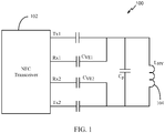
- FIG. 1 is an illustration of a conventional NFC system 100 including an antenna 104 coupled to an NFC transceiver 102.
- NFC system 100 includes two additional receive pins at nodes Rx1 and Rx2, which operate as virtual grounds. Further, series capacitor CVE1 is coupled between antenna 104 and node Rx1 and series capacitor CVE2 is coupled between antenna 104 and node Rx2. Nodes Rx1 and Rx2, which act as virtual grounds, may receive an input current proportional to a voltage at antenna 104. As will be appreciated by a person having ordinary skill, NFC system 100 may exhibit reduced efficiency due to the voltage to current conversion. Further, NFC system 100 may require additional external components.
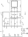
- FIG. 2 illustrates another conventional NFC system 120 including receiver circuitry 122, antenna 124, matching circuit 126, and EMC filter 128.
- Receiver circuitry 122 includes resistors R1 and R2, which together function as a voltage divider. Further, receiver circuitry 122 includes capacitor C vmid , which together with resistor R1, function as a low-pass filter that detects the common-mode value of the input signal that serves as a reference for the signal sampler within the receiver.
- the voltage divider provides protection for NFC system 120, the voltage divider has a fixed ratio and, therefore, is not suitable for operation over a wide dynamic range.
- Exemplary embodiments of the present invention are related to an NFC transceiver, which is configured to adaptively scale the amplitude of a received signal to optimize receiver sensitivity while providing adequate device protection. Furthermore, the NFC transceiver may be configured for adaptive load modulation depth scaling for optimal signal resolution and power harvesting.
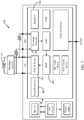
- FIG. 3 is a block diagram of an NFC transceiver 150, which is configured to support both active and passive modes, as mentioned above.
- NFC transceiver 150 includes, among other components, an antenna 151, a digital signal processor (DSP) 152, which is also commonly referred to as a baseband modem, a digital-to-analog converter (DAC) & driver module 154, and a load modulation module 156. It is noted that DAC and driver module 154 may be configured for load modulation and, thus, a separate load modulation module may not be required.
- DSP digital signal processor
- DAC digital-to-analog converter
- driver module 154 may be configured for load modulation and, thus, a separate load modulation module may not be required.
- NFC transceiver 150 further includes an envelope detector 158 and a regulator 160.
- regulator 152 may comprise a rectifier that may be configured to convert an AC input signal to a DC signal. Further, a voltage at an output of the rectifier may be used to determine an amount of power being harvested by an associated transceiver (e.g. transceiver 150).
- an amplitude of an input signal at an NFC transceiver is too high, the transceiver may be damaged. However, if the amplitude of the input signal it too low, the sensitivity of the transceiver may be inadequate.
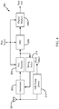
- FIG. 4 is a block diagram of an NFC receiver 200, in accordance with an exemplary embodiment of the present invention.
- NFC transceiver 200 includes an antenna 201, an attenuator 202, an envelope detector 204, an analog-to-digital converter 206, NFC field detect 212, and a digital modem 208.
- attenuator 202 is coupled to and configured to receive an input signal from antenna 201.
- envelope detector 204 is coupled to and configured to receive a signal output from attenuator 202.
- Attenuator 202 may also be referred to herein as an "adaptive attenuator,” and “adjustable loss stage,” or a “voltage divider.”
- envelope detector 204 may be configured to sense an amplitude of the input signal.
- NFC transceiver 200 further includes a swing select 210 configured to receive an output of envelope detector and, in response thereto, convey one or more control signals to attenuator 202 for controlling (i.e., adjusting) an attenuation of attenuator 202.
- swing select 210 may comprise a controller, a processor, digital logic, or the like. "Rate Select" adjusts the operation speed of the ADC depending on the mode of operation in order to achieve the best power efficiency.
- FIG. 5 is one contemplated circuit diagram of an attenuator 300, according to an exemplary embodiment of the present invention.
- attenuator 202 as illustrated in FIG. 4 may comprise attenuator 300 illustrated in FIG. 5 .
- Attenuator 300 which comprises a resistive network, includes a first resistor R1, which is external to a chip 302.
- attenuator 300 includes one or more resistors R2-RN in a parallel configuration and integrated on chip 302.
- resistor R1 may be coupled between an antenna (e.g., antenna 201 illustrated in FIG. 4 ) and chip 302, and may be in series with resistors R2-RN.
- Attenuator 300 may further include transistors M1 R and MN R .
- transistor M1 R is configured to provide a circuit path (i.e., a resistive path) from node N1 R to ground voltage 304 while in a conductive state.
- transistor MN R is configured to provide a circuit path (i.e., a resistive path) from node NN R to ground voltage 304 while in a conductive state.
- each transistor i.e., transistors M1 R -MN R
- Attenuator 300 may be configured to receive an input 306 and convey an output 308.
- FIG. 6 is a contemplated circuit diagram of another attenuator 350, according to an exemplary embodiment of the present invention.
- attenuator 202 may comprise attenuator 350 illustrated in FIG. 6 .
- Attenuator 350 which comprises a capacitive network, includes a first capacitor C1, which is external to a chip 352.
- attenuator 350 includes one or more capacitors C2-CN in a parallel configuration and may be integrated on chip 352.
- capacitor C1 may be coupled between an antenna (e.g., antenna 201 illustrated in FIGS. 4 and 5 ) and chip 352, and may be in parallel with capacitors C2-CN.
- Attenuator 350 may further include transistors M1 C and MN C .
- transistor M1 C is configured to provide a circuit path (i.e., a capacitive path) from node N1 C to ground voltage 304 while in a conductive state.
- transistor MN C is configured to provide a circuit path (i.e., a capacitive path) from node NN C to ground voltage 304 while in a conductive state.
- each transistor i.e., transistors M1 C -MN C
- Attenuator 350 may be configured to receive an input 356 and convey an output 358.
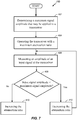
- FIG. 7 is a flowchart illustrating a method 400, in accordance with one or more exemplary embodiments.
- Method 400 may include determining a maximum signal amplitude of an input signal that may be applied to a transceiver (depicted by numeral 402). It is noted that the maximum signal amplitude may be determined during a design stage of the transceiver, as will be appreciated by a person having ordinary skill in the art.
- Method 400 may also include operating the transceiver with a maximum attenuation ratio (depicted by numeral 404). Further, method 400 may include measuring an amplitude of an input signal at the transceiver (depicted by numeral 406).
- step 408 of method 400 includes determining whether the input signal has an amplitude that is less than the maximum signal amplitude. If the amplitude of the input signal is less than the maximum signal amplitude, the attenuation ratio may be decreased (depicted by numeral 412), and method 400 may return to step 406. If the amplitude of the input signal is not less than the maximum signal amplitude, the attenuation ratio may be increased by one step (depicted by numeral 410).
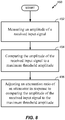
- FIG. 8 is a flowchart illustrating a method 450, in accordance with one or more exemplary embodiments.
- Method 450 may include measuring an amplitude of a received input signal (depicted by numeral 452).
- Method 450 may also include comparing the amplitude of the received input signal to a maximum threshold amplitude (depicted by numeral 454). Further, method 450 adjusting an attenuation ratio of an attenuator in response to comparing the amplitude of the received input signal to the maximum threshold amplitude (depicted by numeral 456).
- a transceiver may be configured to adaptively scale a depth of load modulation to provide for sufficient power harvesting while enabling a load modulation signal to be resolved at an initiator.
- exemplary embodiments of the present invention provide for a calibration mechanism, which maximizes a load modulation depth while enabling for an adequate amount of power to be harvested.
- various exemplary embodiments may utilize systems and devices to enable for programmable load modulation depths.
- DAC current digital-to-analog converter
- FIG. 9 illustrates a system 480 including a current digital-to-analog converter (DAC) 482, according to an exemplary embodiment of the present invention.
- current DAC 482 may also be referred to herein as a "segmented DAC.”
- Current DAC 482 is coupled to an antenna 484 and may be configured to receive one or more digital signals from a digital component, such as, for example only, a filter, such as a digital up-conversion (UPC) filter.
- Current DAC 482 may also be configured to receive one or more control signals from a control module 486, which may comprise, for example only, a processor, a controller, or the like.
- Control module 486 may comprise a mode selector 489 configured to determine whether system 480 should be in an active mode or a passive mode. Control module 486 may determine a mode (i.e., active or passive) of system 480 via one or more sensors, user input, or other suitable, known means. Upon determination of a mode, control module 486 may convey one or more control signals to current DAC 482 for controlling a configuration thereof. It is noted that control module 486 may adjust the signal modulation, data rate, etc, based on the mode of operation.
- current DAC 482 may be configured to drive a current into antenna 484. More specifically, in one operational mode (e.g., an active mode) current DAC 482 may be configured to convey a current directly to antenna 484 and, therefore, in comparison to conventional NFC transmitters, a separate driver may not be required.
- one operational mode e.g., an active mode
- current DAC 482 may be configured to convey a current directly to antenna 484 and, therefore, in comparison to conventional NFC transmitters, a separate driver may not be required.
- an antenna driver which is implemented by current DAC 482 may produce a variety of signal modulations.
- UPC filters may be implemented by digital components without significant area and power penalty, resulting in ease of design and area reduction. More specifically, for example, an up-converter (UPC) and filters within system 480 may be implemented with digital components.
- UPC up-converter
- current DAC 482 may be operated at a multiple of 13.56 MHz for enhanced pulse shaping and, therefore, an electromagnetic compatibility (EMC) filter may not be required.
- FIG. 10 illustrates an array of drivers 488, which is an example of an array of drivers within current DAC 482.
- Each driver 492 i.e., 492_A-492_N
- Each driver 492 includes an associated input 490 (i.e., 490_A-490_N) and, furthermore, array of drivers 488 includes an output 493.
- a current DAC such as current DAC 482
- driver 492_A may include 2 ⁇ 0 cells (i.e., one cell)
- driver 492_B may include 2 ⁇ 1 cells (i.e., two cells)
- driver 492_N-1 may include 2 ⁇ (N-1) cells (e.g., sixteen cells if N is equal to five)
- driver 492_N may include 2 ⁇ N cells (e.g., thirty-two cells if N is equal to five). It is noted that any number of drivers within an array of drivers is within the scope of the invention.
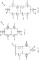
- FIG. 11 illustrates a DAC cell 500, according to an exemplary embodiment of the present invention.
- DAC cell 500 comprises a low-voltage differential signaling (LVDS) driver including a plurality of transistors M1, M2, M3, and M4 and current sources 502 and 503.
- LVDS low-voltage differential signaling
- DAC cell 500 may be configured to receive input signals D p and D n from, for example, control module 486, and output a current I out_1 .
- DAC cell 504 comprises a LVDS driver includes a plurality of transistors M5, M6, M7, and M8 and current source 503.
- DAC cell 504 may be configured to receive input signals V b , D p and D n from, for example, control module 486, and output a current I out_2 . This configuration of DAC cell 504 allows the circuit to run from a lower supply, compared to a typical LVDS approach.
- DAC cell 506 comprises a LVDS driver including a plurality of transistors M9, M12, M13, and M16 and current sources 502 and 503. Further, DAC cell 506 includes cascode devices M10, M11, M14 and M15. As will be appreciated by a person having ordinary skill in the art, a cascode device may improve stress related issues of DAC cell 506, especially at higher voltages (e.g., 1.8 volts). More specifically, cascode devices may provide added protection for devices by reducing the voltage drop across those devices.
- DAC cell 506 may be configured to receive input signals V cas1 , V cas2 , D p and D n from, for example, control module 486 or an analog generation block, and output a current I out_3 .
- a typical technique of NFC is the use of load modulation, in which a device varies a load impedance of its coil to change its resonant frequency and its quality factor Q. This action causes a voltage variation at another device (i.e., a device in an initiator mode).
- a low-voltage differential signaling (LVDS) driver stage may be reconfigured with a plurality of switches to perform load modulation.
- an array of LVDS cells wherein at least one cell includes one or more switches, may enable for adjustment of the strength (i.e., a depth) of load modulation.
- one or more LVDS cells may be configured to provide symmetry in load modulation.
- DAC cell 508 is illustrated.
- DAC cell 508 comprises a LVDS driver including a plurality of transistors M17, M19, M20, M21, M23, and M24 and current sources 502 and 503.
- DAC cell 508 includes cascode devices M18 and M22, which, as noted above, may provide added protection for DAC cell 508.
- DAC cell 508 further includes a plurality of switches S 1-S8, in accordance with an exemplary embodiment of the present invention.
- DAC cell 508 may be configured to receive input signals V cas1 , V DD , D p and D n from, for example, control module 486, output a current T out_4 .
- DAC cell 508 is in an active mode and, therefore, is adapted to drive a current into an associated antenna).
- DAC cell may provide load modulation. During load modulation, current sources 503 and 503 are each off. Further, when S2, S4, S5, and S7 are closed, the circuit effectively resembles a diode (formed by M23) and small resistances (formed by M19, M20, and M24). Effectively, if the voltage swing across the output nodes (Iout_4) is larger than one threshold (Vth), the path turns on and modulates the load.
- cell 508 may be configured such that switches S1, S3, S5, and S7 are on and the rest of the switches are off. Accordingly, cell 508 may still operate in the load modulation mode but the polarity of the hysteresis is alternated. Further, if switches S2, S3, S6, and S8 are on and the rest of switches are off while current sources 502 and 503 are conducting current, then the driver cell operates in the active mode and drives current into the antenna. Further, during a passive mode, one or more of switches S 1-S8 may be reconfigured to adaptively provide various levels of load modulation, as will be appreciated by a person having ordinary skill in the art.
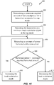
- FIG. 15 is a flowchart illustrating a method 600, in accordance with one or more exemplary embodiments.
- Method 600 may include determining a minimum required amount of harvested power for a transceiver to operate in a tag mode (depicted by numeral 4602). It is noted that the minimum required amount of harvested power may be determined via simulation, as will be appreciated by a person having ordinary skill in the art. Method 600 may also include operating the transceiver at a minimum load modulation depth in the tag mode (depicted by numeral 604). Further, method 600 may include measuring an amount of power harvested by the transceiver (depicted by numeral 606). It is noted that the amount of power harvested may be determined by measuring an amount of power at an output of a rectifier.
- step 608 of method 600 includes determining whether the amount of harvested power is greater than the minimum required amount of harvested power. If the harvested power is greater than the minimum required amount of harvested power, the load modulation depth may be increased (depicted by numeral 610), and method 600 may return to step 606. If the harvested power is not greater than the minimum required amount of harvested power, the load modulation depth may be decreased by one step (depicted by numeral 612).
- FIG. 16 is a flowchart illustrating a method 620, in accordance with one or more exemplary embodiments.
- Method 620 may include measuring an amount of power harvested by a transceiver during load modulation (depicted by numeral 622).
- Method 620 may also include comparing the amount of power harvested to a minimum harvested power threshold (depicted by numeral 624). Further, method 620 adjusting a depth of load modulation in response to comparing the amount of power harvested to the minimum harvested power threshold (depicted by numeral 626).
- FIG. 17 is a block diagram of a NFC transceiver 500, in accordance with one or more embodiments of the present invention.
- NFC transceiver 500 includes antenna 201, a scaling element 702, a sensing element 704, and a controller 706.
- scaling element 702 comprises a programmable load modulation element (e.g., current DAC 482 including a plurality of DAC cells 508) and sensing element 704 comprises a rectifier.
- controller 706 may be configured to receive one or more signals from sensing element 704, compare data (i.e., measured data) from sensing element 704 to stored data (i.e., threshold data) and convey one or more control signals to scaling element 702 for controlling operation thereof.
- scaling element 702 comprises an attenuator (e.g., attenuator 202) and sensing element 704 comprises an envelope detector (e.g., envelope detector 204).
- controller 706 may be configured to receive one or more signals from sensing element 704, compare data (i.e., measured data) from sensing element 704 to stored data (i.e., threshold data) and convey one or more control signals to scaling element 702 for controlling operation thereof.
- DSP Digital Signal Processor
- ASIC Application Specific Integrated Circuit
- FPGA Field Programmable Gate Array
- a general purpose processor may be a microprocessor, but in the alternative, the processor may be any conventional processor, controller, microcontroller, or state machine.
- a processor may also be implemented as a combination of computing devices, e.g., a combination of a DSP and a microprocessor, a plurality of microprocessors, one or more microprocessors in conjunction with a DSP core, or any other such configuration.
- a software module may reside in Random Access Memory (RAM), flash memory, Read Only Memory (ROM), Electrically Programmable ROM (EPROM), Electrically Erasable Programmable ROM (EEPROM), registers, hard disk, a removable disk, a CD-ROM, or any other form of storage medium known in the art.
- An exemplary storage medium is coupled to the processor such that the processor can read information from, and write information to, the storage medium.
- the storage medium may be integral to the processor.
- the processor and the storage medium may reside in an ASIC.
- the ASIC may reside in a user terminal.
- the processor and the storage medium may reside as discrete components in a user terminal.
- the functions described may be implemented in hardware, software, firmware, or any combination thereof. If implemented in software, the functions may be stored on or transmitted over as one or more instructions or code on a computer-readable medium.
- Computer-readable media includes both computer storage media and communication media including any medium that facilitates transfer of a computer program from one place to another.
- a storage media may be any available media that can be accessed by a computer.
- such computer-readable media can comprise RAM, ROM, EEPROM, CD-ROM or other optical disk storage, magnetic disk storage or other magnetic storage devices, or any other medium that can be used to carry or store desired program code in the form of instructions or data structures and that can be accessed by a computer.
- any connection is properly termed a computer-readable medium.
- the software is transmitted from a website, server, or other remote source using a coaxial cable, fiber optic cable, twisted pair, digital subscriber line (DSL), or wireless technologies such as infrared, radio, and microwave
- the coaxial cable, fiber optic cable, twisted pair, DSL, or wireless technologies such as infrared, radio, and microwave are included in the definition of medium.
- Disk and disc includes compact disc (CD), laser disc, optical disc, digital versatile disc (DVD), floppy disk and blu-ray disc where disks usually reproduce data magnetically, while discs reproduce data optically with lasers. Combinations of the above should also be included within the scope of computer-readable media.
Description
- The present invention relates generally to near field communication (NFC). More specifically, the present invention relates to NFC transceivers configured for adaptive signal scaling.
- Near Field Communication (NFC) is a wireless technology that can enable for short-range exchange of information between two or more devices. Devices capable of NFC can simplify presence-oriented transactions to enable for rapid and more secure exchange of information, for example, as in purchases for goods and services, or the exchange of information therein.
- As a person skilled in the art will appreciate and understand, NFC technologies communicate over magnetic field induction, where at least two loop antennas are located within each other's "near field," effectively forming an air-core transformer that operates within a globally available and unlicensed radio frequency which, as indicated, is an industrial, scientific and medical (ISM) band of 13.56 MHz, with a band width of almost two (2) MHz.
- In a conventional NFC system, a trade-off exists between adequate receiver sensitivity and protection from a large signal swing. Further, a trade-off exists between signal resolution and power harvesting during load modulation. A need exists for methods, systems, and devices for adaptive receive signal scaling and adaptive load modulation scaling within NFC systems.
- Attention is drawn to document
EP 2 333 932A1 - This prior art is acknowledged in the preamble of
claims - In accordance with the present invention, a NFC transceiver, as set forth in
claim 1, and a method performed by a NFC transceiver, as set forth inclaim 4, is provided. Further embodiments are claimed in the dependent claims. -
-
FIG. 1 illustrates a conventional NFC system. -
FIG. 2 illustrates another conventional NFC system. -
FIG. 3 is a block diagram of an NFC transceiver, according to an exemplary embodiment of the present invention. -
FIG. 4 is a block diagram of an NFC receiver, in accordance with an exemplary embodiment of the present invention. -
FIG. 5 illustrates an attenuator, according to an exemplary embodiment of the present invention. -
FIG. 6 illustrates another attenuator, according to an exemplary embodiment of the present invention. -
FIG. 7 is a flowchart illustrating a method, according to an exemplary embodiment of the present invention. -
FIG. 8 is a flowchart illustrating another method, according to an exemplary embodiment of the present invention. -
FIG. 9 illustrates an NFC system including a device comprising a current digital-to-analog converter (DAC) coupled to an antenna, in accordance with an exemplary embodiment of the present invention. -
FIG. 10 illustrates an array of drivers within a digital-to-analog converter (DAC), according to an exemplary embodiment of the present invention. -
FIG. 11 illustrates a DAC cell including a low-voltage differential signaling (LVDS) driver, according to an exemplary embodiment of the present invention. -
FIG. 12 illustrates another DAC cell including an LVDS driver, in accordance with an exemplary embodiment of the present invention. -
FIG. 13 illustrates another DAC cell including an LVDS driver, according to an exemplary embodiment of the present invention. -
FIG. 14 depicts yet another DAC cell including an LVDS driver, according to an exemplary embodiment of the present invention. -
FIG. 15 is a flowchart illustrating another method, according to an exemplary embodiment of the present invention. -
FIG. 16 is a flowchart illustrating yet another method, according to an exemplary embodiment of the present invention. -
FIG. 17 depicts an NFC transceiver, according to an exemplary embodiment of the present invention. - The detailed description set forth below in connection with the appended drawings is intended as a description of exemplary embodiments of the present invention and is not intended to represent the only embodiments in which the present invention can be practiced. The term "exemplary" used throughout this description means "serving as an example, instance, or illustration," and should not necessarily be construed as preferred or advantageous over other exemplary embodiments. The detailed description includes specific details for the purpose of providing a thorough understanding of the exemplary embodiments of the invention. It will be apparent to those skilled in the art that the exemplary embodiments of the invention may be practiced without these specific details. In some instances, well-known structures and devices are shown in block diagram form in order to avoid obscuring the novelty of the exemplary embodiments presented herein.
- NFC is a communication standard that enables wireless communication devices, such as cellular telephones, SmartPhones, and personal digital assistants (PDAs) to establish peer-to-peer (P2P) networks. NFC may enable electronic devices to exchange data and initiate applications automatically when they are brought in close proximity, for example ranges from less than a centimeter to a distance of about 10 cm. As non-limiting examples, NFC may enable downloading of images stored in a digital camera to a personal computer, downloading of audio and video entertainment to portable devices, or downloading of data stored in a SmartPhone to a personal computer or other wireless device. NFC may be compatible with smart card technologies and may also be utilized to enable purchase of goods and services. In an exemplary embodiment, the frequency used for NFC is centered at about 13.56 MHz.
- An NFC transceiver may include circuitry to impedance match to an antenna or other circuitry within a coupling element. The NFC transceiver may also include suitable logic, circuitry, processors, code, or combinations thereof to enable the reception and transmission of NFC signals, for which the carrier frequency of the received signal is in the NFC frequency band. Data may be modulated on the carrier frequency.
- Conventional NFC may be based on Radio-Frequency Identification (RFID) technology that uses field induction to enable communication between electronic devices in close proximity. This can enable users to perform intuitive, safe, contactless transactions. Conventional state-of-the art NFC may operate at 13.56 MHz and transfers data at up to 424 Kbits/second. Of course, improvements to NFC technology may result in differing frequency(s), differing throughput values, or both. Communication between two or more NFC-compatible devices may occur when the devices are brought within a short distance from one another and maybe compatible with other known wireless technologies such as Bluetooth or Wi-Fi, for example.
- Currently, there are two principal modes of operation available under present NFC standards: active and passive (i.e., powered by field). In active mode, a device may generate its own radio field to transmit data. In passive mode, one device may generate a radio field, while the other uses load modulation to transfer data. The passive mode of communication is often useful for limited power devices, such as mobile phones and PDAs, which need to minimize energy use. It may also prevent disruption of NFC communication when the device battery runs out.
- In the various exemplary embodiments described herein, the term NFC is understood to encompass any now or future known wireless or near-proximity communication protocols or systems that facilitate the short-range wireless transfer of information, and is understood to not be limited to current standards or protocols promulgated by an NFC standards body or organization. Accordingly, NFC is understood to be applied herein as a generic sense of the term.
- As will be understood by a person having ordinary skill in the art, an input signal to an NFC transceiver may have a large dynamic range. In conventional NFC devices, are large upper limit of the dynamic range may require placement of a voltage divider at the receiver input to protect the devices. However, a voltage divider may reduce receiver sensitivity for the lower limit of the dynamic range.
- Further, a trade off exists between a depth of load modulation for an NFC transmitter in the tag mode trades and the total energy that a transceiver can harvest during the power-by-field (PBF) mode. The optimum depth of modulation can vary depending on the distance, data rate, and the mode of operation. It is therefore essential to identify the maximum modulation depth that can provide sufficient power for the tag to operate.
-
FIG. 1 is an illustration of aconventional NFC system 100 including anantenna 104 coupled to anNFC transceiver 102.NFC system 100 includes two additional receive pins at nodes Rx1 and Rx2, which operate as virtual grounds. Further, series capacitor CVE1 is coupled betweenantenna 104 and node Rx1 and series capacitor CVE2 is coupled betweenantenna 104 and node Rx2. Nodes Rx1 and Rx2, which act as virtual grounds, may receive an input current proportional to a voltage atantenna 104. As will be appreciated by a person having ordinary skill,NFC system 100 may exhibit reduced efficiency due to the voltage to current conversion. Further,NFC system 100 may require additional external components. -
FIG. 2 illustrates anotherconventional NFC system 120 includingreceiver circuitry 122,antenna 124, matchingcircuit 126, andEMC filter 128.Receiver circuitry 122 includes resistors R1 and R2, which together function as a voltage divider. Further,receiver circuitry 122 includes capacitor Cvmid, which together with resistor R1, function as a low-pass filter that detects the common-mode value of the input signal that serves as a reference for the signal sampler within the receiver. Although, the voltage divider provides protection forNFC system 120, the voltage divider has a fixed ratio and, therefore, is not suitable for operation over a wide dynamic range. - Exemplary embodiments of the present invention, as described herein, are related to an NFC transceiver, which is configured to adaptively scale the amplitude of a received signal to optimize receiver sensitivity while providing adequate device protection. Furthermore, the NFC transceiver may be configured for adaptive load modulation depth scaling for optimal signal resolution and power harvesting.
-
FIG. 3 is a block diagram of anNFC transceiver 150, which is configured to support both active and passive modes, as mentioned above.NFC transceiver 150 includes, among other components, anantenna 151, a digital signal processor (DSP) 152, which is also commonly referred to as a baseband modem, a digital-to-analog converter (DAC) &driver module 154, and aload modulation module 156. It is noted that DAC anddriver module 154 may be configured for load modulation and, thus, a separate load modulation module may not be required.NFC transceiver 150 further includes anenvelope detector 158 and aregulator 160. Various components ofNFC transceiver 150, such asenvelope detector 158, DAC anddriver module 154, and aregulator 160, will be discussed more fully below. It is noted thatregulator 152 may comprise a rectifier that may be configured to convert an AC input signal to a DC signal. Further, a voltage at an output of the rectifier may be used to determine an amount of power being harvested by an associated transceiver (e.g. transceiver 150). - As will be appreciated by a person having ordinary skill in the art, if an amplitude of an input signal at an NFC transceiver is too high, the transceiver may be damaged. However, if the amplitude of the input signal it too low, the sensitivity of the transceiver may be inadequate.
-
FIG. 4 is a block diagram of anNFC receiver 200, in accordance with an exemplary embodiment of the present invention.NFC transceiver 200 includes anantenna 201, anattenuator 202, anenvelope detector 204, an analog-to-digital converter 206, NFC field detect 212, and adigital modem 208. As illustrated inFIG. 4 ,attenuator 202 is coupled to and configured to receive an input signal fromantenna 201. Further,envelope detector 204 is coupled to and configured to receive a signal output fromattenuator 202. It is noted thatattenuator 202 may also be referred to herein as an "adaptive attenuator," and "adjustable loss stage," or a "voltage divider." Moreover, as will be appreciated by a person having ordinary skill in the art,envelope detector 204 may be configured to sense an amplitude of the input signal.NFC transceiver 200 further includes a swing select 210 configured to receive an output of envelope detector and, in response thereto, convey one or more control signals toattenuator 202 for controlling (i.e., adjusting) an attenuation ofattenuator 202. It is noted that swing select 210 may comprise a controller, a processor, digital logic, or the like. "Rate Select" adjusts the operation speed of the ADC depending on the mode of operation in order to achieve the best power efficiency. -
FIG. 5 is one contemplated circuit diagram of anattenuator 300, according to an exemplary embodiment of the present invention. It is noted thatattenuator 202, as illustrated inFIG. 4 may compriseattenuator 300 illustrated inFIG. 5 .Attenuator 300, which comprises a resistive network, includes a first resistor R1, which is external to achip 302. Furthermore,attenuator 300 includes one or more resistors R2-RN in a parallel configuration and integrated onchip 302. As illustrated inFIG. 5 , resistor R1 may be coupled between an antenna (e.g.,antenna 201 illustrated inFIG. 4 ) andchip 302, and may be in series with resistors R2-RN.Attenuator 300 may further include transistors M1R and MNR. As will be appreciated by a person having ordinary skill in the art, transistor M1R is configured to provide a circuit path (i.e., a resistive path) from node N1R toground voltage 304 while in a conductive state. Similarly, transistor MNR is configured to provide a circuit path (i.e., a resistive path) from node NNR toground voltage 304 while in a conductive state. More specifically, each transistor (i.e., transistors M1R-MNR) is configured to receive a control signal (i.e., at a respective gate) from swing select 210 (seeFIG. 4 ) and, in response thereto, may operate in either a conductive mode to provide a resistive path or non-conductive mode to provide an open circuit. Accordingly, the number of resistive paths withinattenuator 300 is programmable and, thus, the attenuation ratio ofattenuator 300 is programmable. It is further noted thatattenuator 300 may be configured to receive aninput 306 and convey anoutput 308. -
FIG. 6 is a contemplated circuit diagram of anotherattenuator 350, according to an exemplary embodiment of the present invention. It is noted thatattenuator 202, as illustrated inFIG. 4 , may compriseattenuator 350 illustrated inFIG. 6 .Attenuator 350, which comprises a capacitive network, includes a first capacitor C1, which is external to achip 352. Furthermore,attenuator 350 includes one or more capacitors C2-CN in a parallel configuration and may be integrated onchip 352. As illustrated inFIG. 6 , capacitor C1 may be coupled between an antenna (e.g.,antenna 201 illustrated inFIGS. 4 and5 ) andchip 352, and may be in parallel with capacitors C2-CN.Attenuator 350 may further include transistors M1C and MNC. As will be appreciated by a person having ordinary skill in the art, transistor M1C is configured to provide a circuit path (i.e., a capacitive path) from node N1C toground voltage 304 while in a conductive state. Similarly, transistor MNC is configured to provide a circuit path (i.e., a capacitive path) from node NNC toground voltage 304 while in a conductive state. More specifically, each transistor (i.e., transistors M1C-MNC) is configured to receive a control signal (i.e., at a respective gate) from swing select 210 (seeFIG. 4 ) and, in response thereto, may operate in either a conductive mode to provide a capacitive path or non-conductive mode to provide an open circuit. Accordingly, the number of capacitive paths withinattenuator 350 is programmable and, thus, the attenuation ratio ofattenuator 350 is programmable. It is further noted thatattenuator 350 may be configured to receive aninput 356 and convey anoutput 358. -
FIG. 7 is a flowchart illustrating amethod 400, in accordance with one or more exemplary embodiments.Method 400 may include determining a maximum signal amplitude of an input signal that may be applied to a transceiver (depicted by numeral 402). It is noted that the maximum signal amplitude may be determined during a design stage of the transceiver, as will be appreciated by a person having ordinary skill in the art.Method 400 may also include operating the transceiver with a maximum attenuation ratio (depicted by numeral 404). Further,method 400 may include measuring an amplitude of an input signal at the transceiver (depicted by numeral 406). Further, step 408 ofmethod 400 includes determining whether the input signal has an amplitude that is less than the maximum signal amplitude. If the amplitude of the input signal is less than the maximum signal amplitude, the attenuation ratio may be decreased (depicted by numeral 412), andmethod 400 may return to step 406. If the amplitude of the input signal is not less than the maximum signal amplitude, the attenuation ratio may be increased by one step (depicted by numeral 410). -
FIG. 8 is a flowchart illustrating amethod 450, in accordance with one or more exemplary embodiments.Method 450 may include measuring an amplitude of a received input signal (depicted by numeral 452).Method 450 may also include comparing the amplitude of the received input signal to a maximum threshold amplitude (depicted by numeral 454). Further,method 450 adjusting an attenuation ratio of an attenuator in response to comparing the amplitude of the received input signal to the maximum threshold amplitude (depicted by numeral 456). - As will be appreciated, large depth load modulation by a tag simplifies data recognition by an initiator. However, larger load modulation depth may reduce the total energy harvested by the tag. According to another exemplary embodiment of the present invention, a transceiver may be configured to adaptively scale a depth of load modulation to provide for sufficient power harvesting while enabling a load modulation signal to be resolved at an initiator. Stated another way, exemplary embodiments of the present invention provide for a calibration mechanism, which maximizes a load modulation depth while enabling for an adequate amount of power to be harvested. Accordingly, various exemplary embodiments may utilize systems and devices to enable for programmable load modulation depths. With reference to
FIGS. 9-14 , a current digital-to-analog converter (DAC) will be described. Further, with specific reference toFIG. 14 , programmable load modulation techniques, utilizing the current DAC, will be described. -
FIG. 9 illustrates asystem 480 including a current digital-to-analog converter (DAC) 482, according to an exemplary embodiment of the present invention. It is noted thatcurrent DAC 482 may also be referred to herein as a "segmented DAC."Current DAC 482 is coupled to anantenna 484 and may be configured to receive one or more digital signals from a digital component, such as, for example only, a filter, such as a digital up-conversion (UPC) filter.Current DAC 482 may also be configured to receive one or more control signals from acontrol module 486, which may comprise, for example only, a processor, a controller, or the like.Control module 486 may comprise amode selector 489 configured to determine whethersystem 480 should be in an active mode or a passive mode.Control module 486 may determine a mode (i.e., active or passive) ofsystem 480 via one or more sensors, user input, or other suitable, known means. Upon determination of a mode,control module 486 may convey one or more control signals tocurrent DAC 482 for controlling a configuration thereof. It is noted thatcontrol module 486 may adjust the signal modulation, data rate, etc, based on the mode of operation. - Further, as described more fully below,
current DAC 482 may be configured to drive a current intoantenna 484. More specifically, in one operational mode (e.g., an active mode)current DAC 482 may be configured to convey a current directly toantenna 484 and, therefore, in comparison to conventional NFC transmitters, a separate driver may not be required. - It is noted that an antenna driver, which is implemented by
current DAC 482, may produce a variety of signal modulations. Further, at finer process nodes (e.g., CMOS process nodes), UPC filters may be implemented by digital components without significant area and power penalty, resulting in ease of design and area reduction. More specifically, for example, an up-converter (UPC) and filters withinsystem 480 may be implemented with digital components. It is noted thatcurrent DAC 482 may be operated at a multiple of 13.56 MHz for enhanced pulse shaping and, therefore, an electromagnetic compatibility (EMC) filter may not be required. -
FIG. 10 illustrates an array ofdrivers 488, which is an example of an array of drivers withincurrent DAC 482. Each driver 492 (i.e., 492_A-492_N) includes an associated input 490 (i.e., 490_A-490_N) and, furthermore, array ofdrivers 488 includes an output 493. As will be understood by a person having ordinary skill in the art, a current DAC, such ascurrent DAC 482, may include an array of drivers wherein eachdriver 492 includes one or more cells. For example, driver 492_A may include 2^0 cells (i.e., one cell), driver 492_B may include 2^1 cells (i.e., two cells), driver 492_N-1 may include 2^(N-1) cells (e.g., sixteen cells if N is equal to five), and driver 492_N may include 2^N cells (e.g., thirty-two cells if N is equal to five). It is noted that any number of drivers within an array of drivers is within the scope of the invention. -
FIG. 11 illustrates aDAC cell 500, according to an exemplary embodiment of the present invention.DAC cell 500 comprises a low-voltage differential signaling (LVDS) driver including a plurality of transistors M1, M2, M3, and M4 andcurrent sources DAC cell 500 may be configured to receive input signals Dp and Dn from, for example,control module 486, and output a current Iout_1. In a contemplated operation, the bias current is switched into the antenna according to the data input. It uses four MOS switches (M1-M4) in a bridged configuration. If switches M1 and M4 are on (Dp=0 & Din=1), the polarity of the output current is positive. On the contrary, if switches M2 and M3 are on (Dp=1 & Dn=0), the polarity of the output current is negative. It is noted that the present invention is not limited toDAC cell 500 and other cells designs may be within the scope of the invention. For example, with reference toFIG. 12 , aDAC cell 504 is illustrated.DAC cell 504 comprises a LVDS driver includes a plurality of transistors M5, M6, M7, and M8 andcurrent source 503. As will be appreciated by a person having ordinary skill in the art,DAC cell 504 may be configured to receive input signals Vb, Dp and Dn from, for example,control module 486, and output a current Iout_2. This configuration ofDAC cell 504 allows the circuit to run from a lower supply, compared to a typical LVDS approach. - Another
DAC cell 506, according to an exemplary embodiment of the present invention, is illustrated inFIG. 13 .DAC cell 506 comprises a LVDS driver including a plurality of transistors M9, M12, M13, and M16 andcurrent sources DAC cell 506 includes cascode devices M10, M11, M14 and M15. As will be appreciated by a person having ordinary skill in the art, a cascode device may improve stress related issues ofDAC cell 506, especially at higher voltages (e.g., 1.8 volts). More specifically, cascode devices may provide added protection for devices by reducing the voltage drop across those devices. As will be appreciated by a person having ordinary skill in the art,DAC cell 506 may be configured to receive input signals Vcas1, Vcas2, Dp and Dn from, for example,control module 486 or an analog generation block, and output a current Iout_3. - As will be appreciated by a person having ordinary skill in the art, a typical technique of NFC is the use of load modulation, in which a device varies a load impedance of its coil to change its resonant frequency and its quality factor Q. This action causes a voltage variation at another device (i.e., a device in an initiator mode).
- In accordance with an exemplary embodiment of the present invention, a low-voltage differential signaling (LVDS) driver stage may be reconfigured with a plurality of switches to perform load modulation. Further, an array of LVDS cells, wherein at least one cell includes one or more switches, may enable for adjustment of the strength (i.e., a depth) of load modulation. Moreover, one or more LVDS cells may be configured to provide symmetry in load modulation. With reference to
FIG. 14 , aDAC cell 508 is illustrated.DAC cell 508 comprises a LVDS driver including a plurality of transistors M17, M19, M20, M21, M23, and M24 andcurrent sources DAC cell 508 includes cascode devices M18 and M22, which, as noted above, may provide added protection forDAC cell 508.DAC cell 508 further includes a plurality of switches S 1-S8, in accordance with an exemplary embodiment of the present invention. As will be appreciated by a person having ordinary skill in the art,DAC cell 508 may be configured to receive input signals Vcas1, VDD, Dp and Dn from, for example,control module 486, output a current Tout_4. - It is noted that in the configuration illustrated in
FIG. 14 (i.e., switches S1, S4, S5, and S7 are closed and switches S2, S3, S6, and S8 are open),DAC cell 508 is in an active mode and, therefore, is adapted to drive a current into an associated antenna). In other contemplated configurations, DAC cell may provide load modulation. During load modulation,current sources cell 508 may be configured such that switches S1, S3, S5, and S7 are on and the rest of the switches are off. Accordingly,cell 508 may still operate in the load modulation mode but the polarity of the hysteresis is alternated. Further, if switches S2, S3, S6, and S8 are on and the rest of switches are off whilecurrent sources -
FIG. 15 is a flowchart illustrating amethod 600, in accordance with one or more exemplary embodiments.Method 600 may include determining a minimum required amount of harvested power for a transceiver to operate in a tag mode (depicted by numeral 4602). It is noted that the minimum required amount of harvested power may be determined via simulation, as will be appreciated by a person having ordinary skill in the art.Method 600 may also include operating the transceiver at a minimum load modulation depth in the tag mode (depicted by numeral 604). Further,method 600 may include measuring an amount of power harvested by the transceiver (depicted by numeral 606). It is noted that the amount of power harvested may be determined by measuring an amount of power at an output of a rectifier. Further, step 608 ofmethod 600 includes determining whether the amount of harvested power is greater than the minimum required amount of harvested power. If the harvested power is greater than the minimum required amount of harvested power, the load modulation depth may be increased (depicted by numeral 610), andmethod 600 may return to step 606. If the harvested power is not greater than the minimum required amount of harvested power, the load modulation depth may be decreased by one step (depicted by numeral 612). -
FIG. 16 is a flowchart illustrating amethod 620, in accordance with one or more exemplary embodiments.Method 620 may include measuring an amount of power harvested by a transceiver during load modulation (depicted by numeral 622).Method 620 may also include comparing the amount of power harvested to a minimum harvested power threshold (depicted by numeral 624). Further,method 620 adjusting a depth of load modulation in response to comparing the amount of power harvested to the minimum harvested power threshold (depicted by numeral 626). -
FIG. 17 is a block diagram of aNFC transceiver 500, in accordance with one or more embodiments of the present invention. As illustrated,NFC transceiver 500 includesantenna 201, ascaling element 702, asensing element 704, and acontroller 706. According to one exemplary embodiment, scalingelement 702 comprises a programmable load modulation element (e.g.,current DAC 482 including a plurality of DAC cells 508) andsensing element 704 comprises a rectifier. In this exemplary embodiment,controller 706 may be configured to receive one or more signals from sensingelement 704, compare data (i.e., measured data) fromsensing element 704 to stored data (i.e., threshold data) and convey one or more control signals to scalingelement 702 for controlling operation thereof. - According to another exemplary embodiment, scaling
element 702 comprises an attenuator (e.g., attenuator 202) andsensing element 704 comprises an envelope detector (e.g., envelope detector 204). In this exemplary embodiment,controller 706 may be configured to receive one or more signals from sensingelement 704, compare data (i.e., measured data) fromsensing element 704 to stored data (i.e., threshold data) and convey one or more control signals to scalingelement 702 for controlling operation thereof. - Those of skill in the art would understand that information and signals may be represented using any of a variety of different technologies and techniques. For example, data, instructions, commands, information, signals, bits, symbols, and chips that may be referenced throughout the above description may be represented by voltages, currents, electromagnetic waves, magnetic fields or particles, optical fields or particles, or any combination thereof.
- Those of skill would further appreciate that the various illustrative logical blocks, modules, circuits, and algorithm steps described in connection with the exemplary embodiments disclosed herein may be implemented as electronic hardware, computer software, or combinations of both. To clearly illustrate this interchangeability of hardware and software, various illustrative components, blocks, modules, circuits, and steps have been described above generally in terms of their functionality. Whether such functionality is implemented as hardware or software depends upon the particular application and design constraints imposed on the overall system. Skilled artisans may implement the described functionality in varying ways for each particular application, but such implementation decisions should not be interpreted as causing a departure from the scope of the exemplary embodiments of the invention.
- The various illustrative logical blocks, modules, and circuits described in connection with the exemplary embodiments disclosed herein may be implemented or performed with a general purpose processor, a Digital Signal Processor (DSP), an Application Specific Integrated Circuit (ASIC), a Field Programmable Gate Array (FPGA) or other programmable logic device, discrete gate or transistor logic, discrete hardware components, or any combination thereof designed to perform the functions described herein. A general purpose processor may be a microprocessor, but in the alternative, the processor may be any conventional processor, controller, microcontroller, or state machine. A processor may also be implemented as a combination of computing devices, e.g., a combination of a DSP and a microprocessor, a plurality of microprocessors, one or more microprocessors in conjunction with a DSP core, or any other such configuration.
- The steps of a method or algorithm described in connection with the exemplary embodiments disclosed herein may be embodied directly in hardware, in a software module executed by a processor, or in a combination of the two. A software module may reside in Random Access Memory (RAM), flash memory, Read Only Memory (ROM), Electrically Programmable ROM (EPROM), Electrically Erasable Programmable ROM (EEPROM), registers, hard disk, a removable disk, a CD-ROM, or any other form of storage medium known in the art. An exemplary storage medium is coupled to the processor such that the processor can read information from, and write information to, the storage medium. In the alternative, the storage medium may be integral to the processor. The processor and the storage medium may reside in an ASIC. The ASIC may reside in a user terminal. In the alternative, the processor and the storage medium may reside as discrete components in a user terminal.
- In one or more exemplary embodiments, the functions described may be implemented in hardware, software, firmware, or any combination thereof. If implemented in software, the functions may be stored on or transmitted over as one or more instructions or code on a computer-readable medium. Computer-readable media includes both computer storage media and communication media including any medium that facilitates transfer of a computer program from one place to another. A storage media may be any available media that can be accessed by a computer. By way of example, and not limitation, such computer-readable media can comprise RAM, ROM, EEPROM, CD-ROM or other optical disk storage, magnetic disk storage or other magnetic storage devices, or any other medium that can be used to carry or store desired program code in the form of instructions or data structures and that can be accessed by a computer. Also, any connection is properly termed a computer-readable medium. For example, if the software is transmitted from a website, server, or other remote source using a coaxial cable, fiber optic cable, twisted pair, digital subscriber line (DSL), or wireless technologies such as infrared, radio, and microwave, then the coaxial cable, fiber optic cable, twisted pair, DSL, or wireless technologies such as infrared, radio, and microwave are included in the definition of medium. Disk and disc, as used herein, includes compact disc (CD), laser disc, optical disc, digital versatile disc (DVD), floppy disk and blu-ray disc where disks usually reproduce data magnetically, while discs reproduce data optically with lasers. Combinations of the above should also be included within the scope of computer-readable media.
- The previous description of the disclosed exemplary embodiments is provided to enable any person skilled in the art to make or use the present invention. Various modifications to these exemplary embodiments will be readily apparent to those skilled in the art, and the generic principles defined herein may be applied to other embodiments without departing from the scope of the invention.
Claims (6)
- A near field communication, NFC, transceiver, comprising:a programmable load modulation element (702) configured for load modulation in a tag mode;a sensing element (704) for measuring an amount of power harvested by the transceiver in the tag mode; anda controller (706) coupled to each of the programmable load modulation element and the sensing element and configured to:compare the measured amount of power harvested to a minimum harvested power threshold, characterized by adjusting a depth of load modulation of the programmable load modulation element based on the comparison, wherein the depth of load modulation is increased if the measured amount of power harvested is greater than the minimum harvested power threshold, and wherein the depth of load modulation is decreased if the measured amount of power harvested is less than the minimum harvested power threshold.
- The transceiver of claim 1, the programmable load modulation element (702) comprising a current digital-to-analog converter, DAC.
- The transceiver of claim 1, the sensing element (704) comprising a rectifier.
- A method (600, 620) performed by a near field communication, NFC, transceiver, the method comprising:performing load modulation in a tag mode;measuring (606, 622) an amount of power harvested by a transceiver during the tag mode;comparing (608, 624) the amount of power harvested to a minimum harvested power threshold; characterized byadjusting (626) a depth of load modulation based on the comparison, whereinthe depth of load modulation is increased (610) if the measured amount of power harvested is greater than the minimum harvested power threshold, and wherein the depth of load modulation is decreased (612) if the measured amount of power harvested is less than the minimum harvested power threshold.
- The method (600, 620) of claim 4, the measuring (606, 622) an amount of power harvested comprising measuring an amount of power at an output of a rectifier.
- The method (600, 620) of claim 4, the adjusting (626) comprising adjusting the depth of load modulation with one or more drivers of a current DAC.
Applications Claiming Priority (2)
| Application Number | Priority Date | Filing Date | Title |
|---|---|---|---|
| US13/282,328 US9384373B2 (en) | 2011-10-26 | 2011-10-26 | Adaptive signal scaling in NFC transceivers |
| PCT/US2012/062286 WO2013063514A2 (en) | 2011-10-26 | 2012-10-26 | Adaptive signal scaling in nfc transceivers |
Publications (2)
| Publication Number | Publication Date |
|---|---|
| EP2771838A2 EP2771838A2 (en) | 2014-09-03 |
| EP2771838B1 true EP2771838B1 (en) | 2017-03-08 |
Family
ID=47178348
Family Applications (1)
| Application Number | Title | Priority Date | Filing Date |
|---|---|---|---|
| EP12784841.4A Active EP2771838B1 (en) | 2011-10-26 | 2012-10-26 | Adaptive signal scaling in nfc transceivers |
Country Status (7)
| Country | Link |
|---|---|
| US (1) | US9384373B2 (en) |
| EP (1) | EP2771838B1 (en) |
| JP (1) | JP2014532927A (en) |
| KR (1) | KR101621045B1 (en) |
| CN (1) | CN104025112B (en) |
| IN (1) | IN2014CN02489A (en) |
| WO (1) | WO2013063514A2 (en) |
Families Citing this family (22)
| Publication number | Priority date | Publication date | Assignee | Title |
|---|---|---|---|---|
| US8811930B2 (en) * | 2011-06-30 | 2014-08-19 | Broadcom Corporation | Wireless peripheral device powered by harvested power generated by wireless communication |
| US8686887B2 (en) * | 2011-10-26 | 2014-04-01 | Qualcomm Incorporated | NFC transceiver with current converter |
| US10037522B2 (en) * | 2012-01-17 | 2018-07-31 | Raytheon Bbn Technologies Corp. | Near-field communication (NFC) system and method for private near-field communication |
| US8909140B2 (en) * | 2012-05-02 | 2014-12-09 | Cambridge Silicon Radio Limited | Transmitter |
| CN110557174A (en) * | 2013-09-04 | 2019-12-10 | 联发科技(新加坡)私人有限公司 | envelope extraction apparatus, signal decoding apparatus, short-range contactless communication apparatus, and related methods |
| KR102155199B1 (en) * | 2013-12-23 | 2020-09-11 | 삼성전자주식회사 | Matching circuit, NFC device and electronic system including the same |
| KR102139552B1 (en) | 2014-04-11 | 2020-07-31 | 삼성전자주식회사 | Wireless communication device and operating method thereof |
| CN104298152B (en) * | 2014-09-29 | 2017-01-25 | 飞天诚信科技股份有限公司 | Near-field communication modulation depth adaptive method and device |
| US9553747B2 (en) | 2014-12-23 | 2017-01-24 | Qualcomm Incorporated | Systems and methods for switching quality factors during inductively coupled communications |
| US9969355B2 (en) * | 2015-10-09 | 2018-05-15 | Nxp B.V. | Integrated circuit device and method for dual-mode transponder communication |
| CN105448237A (en) * | 2016-01-11 | 2016-03-30 | 深圳市芯联电子科技有限公司 | LED display apparatus controlled and driven by use of NFC |
| CN107437960B (en) * | 2016-05-27 | 2021-09-07 | 鸿富锦精密工业(深圳)有限公司 | Near field communication device and system |
| FR3052930B1 (en) * | 2016-06-17 | 2019-06-28 | Continental Automotive France | RECHARGEABLE ELECTRONIC UNIT FOR MOTOR VEHICLE |
| US10659009B2 (en) * | 2016-08-01 | 2020-05-19 | Nxp B.V. | Method and system for attenuator phase compensation |
| US10110281B2 (en) * | 2017-03-17 | 2018-10-23 | Nxp B.V. | Near field communication device |
| KR102603180B1 (en) * | 2017-12-14 | 2023-11-16 | 삼성전자주식회사 | Modulation index setting circuit of NFC device, NFC device and method of operating the NFC device |
| CN108446576B (en) * | 2018-01-17 | 2021-02-05 | 艾体威尔电子技术(北京)有限公司 | Terminal modulation depth self-adaption method |
| US10893597B2 (en) | 2018-06-25 | 2021-01-12 | Fanlight Co., Ltd. | Group-performance control method using light-emitting devices |
| JP6860039B2 (en) * | 2019-06-24 | 2021-04-14 | セイコーエプソン株式会社 | Control devices and electronic devices |
| KR20210077180A (en) | 2019-12-17 | 2021-06-25 | 삼성전자주식회사 | Near field communication reader, operation method of near field communication reader, and operation method of electronic device including near field communication reader |
| CN111210753B (en) * | 2020-01-23 | 2023-06-09 | 京东方科技集团股份有限公司 | Display driving circuit, display driving method and display device |
| JP2022135501A (en) * | 2021-03-05 | 2022-09-15 | キヤノン株式会社 | Power receiving device, control method for the same, and program |
Family Cites Families (39)
| Publication number | Priority date | Publication date | Assignee | Title |
|---|---|---|---|---|
| JPH10240889A (en) | 1997-02-27 | 1998-09-11 | Kokusai Electric Co Ltd | Noncontact ic card |
| US5955870A (en) * | 1997-09-29 | 1999-09-21 | Intel Corporation | Multi-mode low power voltage regulator |
| US7260371B1 (en) | 1998-04-14 | 2007-08-21 | The Goodyear Tire & Rubber Company | Programmable modulation index for transponder |
| EP1188144B1 (en) | 1999-05-17 | 2003-12-17 | The Goodyear Tire & Rubber Company | Rf transponder and method for controlling rf signal modulation in a passive transponder |
| US8373544B2 (en) | 2003-10-29 | 2013-02-12 | Innovision Research & Technology Plc | RFID apparatus |
| US7689195B2 (en) | 2005-02-22 | 2010-03-30 | Broadcom Corporation | Multi-protocol radio frequency identification transponder tranceiver |
| US20070026825A1 (en) * | 2005-02-24 | 2007-02-01 | Innovision Research & Technology Plc | NFC device and apparatus |
| US20060197650A1 (en) * | 2005-03-02 | 2006-09-07 | Magnadyne Corporation | Passive transmitter |
| US20060273882A1 (en) * | 2005-06-01 | 2006-12-07 | Intel Corporation | RFID tag with separate transmit and receive clocks and related method |
| FR2892212A1 (en) * | 2005-10-17 | 2007-04-20 | St Microelectronics Sa | NFC READER HAVING PASSIVE OPERATING MODE WITH LOW POWER CONSUMPTION |
| US8947233B2 (en) * | 2005-12-09 | 2015-02-03 | Tego Inc. | Methods and systems of a multiple radio frequency network node RFID tag |
| GB0525635D0 (en) * | 2005-12-16 | 2006-01-25 | Innovision Res & Tech Plc | Chip card and method of data communication |
| JP4355711B2 (en) | 2006-04-20 | 2009-11-04 | フェリカネットワークス株式会社 | Information processing terminal, IC card, portable communication device, wireless communication method, and program |
| ES2676623T3 (en) * | 2006-04-24 | 2018-07-23 | Nokia Technologies Oy | System and method for managing and controlling near-field communication for a mobile multifunctional device when the device is not charged or is only partially charged |
| JP5325415B2 (en) | 2006-12-18 | 2013-10-23 | 株式会社半導体エネルギー研究所 | Semiconductor device |
| FR2914800B1 (en) * | 2007-04-04 | 2010-09-17 | Jacek Kowalski | NFC MODULE, IN PARTICULAR FOR MOBILE TELEPHONE |
| US20080268803A1 (en) * | 2007-04-25 | 2008-10-30 | Guillaume Blin | Techniques for antenna retuning utilizing receive power information |
| US8520692B2 (en) * | 2007-10-31 | 2013-08-27 | Qualcomm Incorporated | Methods and apparatus related to controlling traffic in a wireless communications system using shared air link traffic resources |
| GB0801225D0 (en) * | 2008-01-23 | 2008-02-27 | Innovision Res & Tech Plc | Near field RF communications |
| JP4637204B2 (en) * | 2008-04-30 | 2011-02-23 | フェリカネットワークス株式会社 | Communication apparatus and antenna characteristic control method |
| JP2009302953A (en) | 2008-06-13 | 2009-12-24 | Toshiba Corp | Noncontact data communications device |
| US8224277B2 (en) | 2008-09-26 | 2012-07-17 | Semiconductor Energy Laboratory Co., Ltd. | Semiconductor device |
| EP2333932A4 (en) | 2008-09-29 | 2015-12-30 | Murata Manufacturing Co | Non-contact power receiving circuit and non-contact power transmission system |
| NZ593772A (en) * | 2009-01-06 | 2013-09-27 | Access Business Group Int Llc | Communication across an inductive link with a dynamic load |
| JP5424459B2 (en) * | 2009-03-05 | 2014-02-26 | パナソニック株式会社 | Electronics |
| US8134410B1 (en) * | 2009-06-22 | 2012-03-13 | Pmc-Sierra, Inc. | Transceiver gain calibration |
| PL2446600T3 (en) * | 2009-06-25 | 2017-03-31 | Koninklijke Philips N.V. | Method and device for processing data packets |
| JP2011015005A (en) * | 2009-06-30 | 2011-01-20 | Panasonic Corp | Antenna device, and portable wireless apparatus provided with the same |
| US8706053B2 (en) | 2009-11-19 | 2014-04-22 | Sony Corporation | Communications circuitry for an electronic device |
| EP2330538A1 (en) | 2009-11-30 | 2011-06-08 | Nxp B.V. | Radio frequency transponder |
| US8686685B2 (en) * | 2009-12-25 | 2014-04-01 | Golba, Llc | Secure apparatus for wirelessly transferring power and communicating with one or more slave devices |
| US9027840B2 (en) * | 2010-04-08 | 2015-05-12 | Access Business Group International Llc | Point of sale inductive systems and methods |
| US8897699B2 (en) * | 2010-05-20 | 2014-11-25 | Broadcom Corporation | Reducing emissions in a near field communications (NFC) capable device |
| CA2752716C (en) * | 2010-09-21 | 2019-04-30 | Inside Secure | Nfc card sensitive to foucault currents |
| US9013896B2 (en) * | 2010-12-30 | 2015-04-21 | Echostar Technologies L.L.C. | Apparatus, systems and methods for power supply employing single-stage forward voltage conversion |
| US9030052B2 (en) * | 2011-05-17 | 2015-05-12 | Samsung Electronics Co., Ltd. | Apparatus and method for using near field communication and wireless power transmission |
| US20130049674A1 (en) * | 2011-08-24 | 2013-02-28 | Qualcomm Incorporated | Integrated photo voltaic solar plant and electric vehicle charging station and method of operation |
| US20130078914A1 (en) * | 2011-09-23 | 2013-03-28 | Broadcom Corporation | Varying Load Modulation in an NFC-Enabled Device Over a Range of Field Strength |
| US9026041B2 (en) * | 2011-11-10 | 2015-05-05 | Avery Dennison Corporation | Portable radio-frequency repeater |
-
2011
- 2011-10-26 US US13/282,328 patent/US9384373B2/en not_active Expired - Fee Related
-
2012
- 2012-10-26 WO PCT/US2012/062286 patent/WO2013063514A2/en active Application Filing
- 2012-10-26 IN IN2489CHN2014 patent/IN2014CN02489A/en unknown
- 2012-10-26 EP EP12784841.4A patent/EP2771838B1/en active Active
- 2012-10-26 CN CN201280053129.8A patent/CN104025112B/en active Active
- 2012-10-26 JP JP2014539088A patent/JP2014532927A/en active Pending
- 2012-10-26 KR KR1020147014070A patent/KR101621045B1/en not_active IP Right Cessation
Non-Patent Citations (1)
| Title |
|---|
| None * |
Also Published As
| Publication number | Publication date |
|---|---|
| CN104025112B (en) | 2018-10-19 |
| WO2013063514A3 (en) | 2013-06-13 |
| KR20140096315A (en) | 2014-08-05 |
| KR101621045B1 (en) | 2016-05-13 |
| CN104025112A (en) | 2014-09-03 |
| US9384373B2 (en) | 2016-07-05 |
| US20130109304A1 (en) | 2013-05-02 |
| EP2771838A2 (en) | 2014-09-03 |
| JP2014532927A (en) | 2014-12-08 |
| WO2013063514A2 (en) | 2013-05-02 |
| IN2014CN02489A (en) | 2015-06-26 |
Similar Documents
| Publication | Publication Date | Title |
|---|---|---|
| EP2771838B1 (en) | Adaptive signal scaling in nfc transceivers | |
| US9292782B2 (en) | Adaptive NFC transceivers | |
| US8686887B2 (en) | NFC transceiver with current converter | |
| US8503931B2 (en) | Tuneable NFC-enabled device | |
| US7881665B2 (en) | Near field communications, NFC, communicators and NFC communications enabled devices | |
| US9553747B2 (en) | Systems and methods for switching quality factors during inductively coupled communications | |
| US8150321B2 (en) | Near field RF communicators and near field communications enabled devices | |
| US8965279B2 (en) | Recovering data in a near field communications apparatus | |
| EP2388930B1 (en) | Overvoltage protection in a near field communications (NFC) capable device | |
| EP2771839B1 (en) | Nfc transceiver utilizing common circuitry for active and passive modes | |
| CN108076448A (en) | For the automated power control in communicator(APC)Method and system | |
| CN108206709A (en) | For operating the method and system of communication device to communicate via inductive coupling | |
| EP4016389B1 (en) | Rfid tag | |
| US20130176111A1 (en) | Radio frequency identification system | |
| EP4016390A1 (en) | Dual system rfid tag | |
| CN115769502A (en) | Frequency division coordinated automatic power control for near field communication | |
| WO2021151229A1 (en) | Devices and methods for near-field communication detection | |
| CN101542927B (en) | Signal transmission system |
Legal Events
| Date | Code | Title | Description |
|---|---|---|---|
| PUAI | Public reference made under article 153(3) epc to a published international application that has entered the european phase |
Free format text: ORIGINAL CODE: 0009012 |
|
| 17P | Request for examination filed |
Effective date: 20140526 |
|
| AK | Designated contracting states |
Kind code of ref document: A2 Designated state(s): AL AT BE BG CH CY CZ DE DK EE ES FI FR GB GR HR HU IE IS IT LI LT LU LV MC MK MT NL NO PL PT RO RS SE SI SK SM TR |
|
| DAX | Request for extension of the european patent (deleted) | ||
| 17Q | First examination report despatched |
Effective date: 20160112 |
|
| GRAP | Despatch of communication of intention to grant a patent |
Free format text: ORIGINAL CODE: EPIDOSNIGR1 |
|
| INTG | Intention to grant announced |
Effective date: 20160923 |
|
| GRAS | Grant fee paid |
Free format text: ORIGINAL CODE: EPIDOSNIGR3 |
|
| GRAA | (expected) grant |
Free format text: ORIGINAL CODE: 0009210 |
|
| AK | Designated contracting states |
Kind code of ref document: B1 Designated state(s): AL AT BE BG CH CY CZ DE DK EE ES FI FR GB GR HR HU IE IS IT LI LT LU LV MC MK MT NL NO PL PT RO RS SE SI SK SM TR |
|
| REG | Reference to a national code |
Ref country code: GB Ref legal event code: FG4D |
|
| REG | Reference to a national code |
Ref country code: CH Ref legal event code: EP Ref country code: AT Ref legal event code: REF Ref document number: 874122 Country of ref document: AT Kind code of ref document: T Effective date: 20170315 |
|
| REG | Reference to a national code |
Ref country code: IE Ref legal event code: FG4D |
|
| REG | Reference to a national code |
Ref country code: DE Ref legal event code: R096 Ref document number: 602012029623 Country of ref document: DE |
|
| REG | Reference to a national code |
Ref country code: LT Ref legal event code: MG4D |
|
| REG | Reference to a national code |
Ref country code: NL Ref legal event code: MP Effective date: 20170308 |
|
| PG25 | Lapsed in a contracting state [announced via postgrant information from national office to epo] |
Ref country code: LT Free format text: LAPSE BECAUSE OF FAILURE TO SUBMIT A TRANSLATION OF THE DESCRIPTION OR TO PAY THE FEE WITHIN THE PRESCRIBED TIME-LIMIT Effective date: 20170308 Ref country code: NO Free format text: LAPSE BECAUSE OF FAILURE TO SUBMIT A TRANSLATION OF THE DESCRIPTION OR TO PAY THE FEE WITHIN THE PRESCRIBED TIME-LIMIT Effective date: 20170608 Ref country code: FI Free format text: LAPSE BECAUSE OF FAILURE TO SUBMIT A TRANSLATION OF THE DESCRIPTION OR TO PAY THE FEE WITHIN THE PRESCRIBED TIME-LIMIT Effective date: 20170308 Ref country code: GR Free format text: LAPSE BECAUSE OF FAILURE TO SUBMIT A TRANSLATION OF THE DESCRIPTION OR TO PAY THE FEE WITHIN THE PRESCRIBED TIME-LIMIT Effective date: 20170609 Ref country code: HR Free format text: LAPSE BECAUSE OF FAILURE TO SUBMIT A TRANSLATION OF THE DESCRIPTION OR TO PAY THE FEE WITHIN THE PRESCRIBED TIME-LIMIT Effective date: 20170308 |
|
| REG | Reference to a national code |
Ref country code: AT Ref legal event code: MK05 Ref document number: 874122 Country of ref document: AT Kind code of ref document: T Effective date: 20170308 |
|
| PG25 | Lapsed in a contracting state [announced via postgrant information from national office to epo] |
Ref country code: LV Free format text: LAPSE BECAUSE OF FAILURE TO SUBMIT A TRANSLATION OF THE DESCRIPTION OR TO PAY THE FEE WITHIN THE PRESCRIBED TIME-LIMIT Effective date: 20170308 Ref country code: ES Free format text: LAPSE BECAUSE OF FAILURE TO SUBMIT A TRANSLATION OF THE DESCRIPTION OR TO PAY THE FEE WITHIN THE PRESCRIBED TIME-LIMIT Effective date: 20170308 Ref country code: RS Free format text: LAPSE BECAUSE OF FAILURE TO SUBMIT A TRANSLATION OF THE DESCRIPTION OR TO PAY THE FEE WITHIN THE PRESCRIBED TIME-LIMIT Effective date: 20170308 Ref country code: SE Free format text: LAPSE BECAUSE OF FAILURE TO SUBMIT A TRANSLATION OF THE DESCRIPTION OR TO PAY THE FEE WITHIN THE PRESCRIBED TIME-LIMIT Effective date: 20170308 Ref country code: BG Free format text: LAPSE BECAUSE OF FAILURE TO SUBMIT A TRANSLATION OF THE DESCRIPTION OR TO PAY THE FEE WITHIN THE PRESCRIBED TIME-LIMIT Effective date: 20170608 |
|
| REG | Reference to a national code |
Ref country code: FR Ref legal event code: PLFP Year of fee payment: 6 |
|
| PG25 | Lapsed in a contracting state [announced via postgrant information from national office to epo] |
Ref country code: NL Free format text: LAPSE BECAUSE OF FAILURE TO SUBMIT A TRANSLATION OF THE DESCRIPTION OR TO PAY THE FEE WITHIN THE PRESCRIBED TIME-LIMIT Effective date: 20170308 |
|
| PG25 | Lapsed in a contracting state [announced via postgrant information from national office to epo] |
Ref country code: SK Free format text: LAPSE BECAUSE OF FAILURE TO SUBMIT A TRANSLATION OF THE DESCRIPTION OR TO PAY THE FEE WITHIN THE PRESCRIBED TIME-LIMIT Effective date: 20170308 Ref country code: RO Free format text: LAPSE BECAUSE OF FAILURE TO SUBMIT A TRANSLATION OF THE DESCRIPTION OR TO PAY THE FEE WITHIN THE PRESCRIBED TIME-LIMIT Effective date: 20170308 Ref country code: AT Free format text: LAPSE BECAUSE OF FAILURE TO SUBMIT A TRANSLATION OF THE DESCRIPTION OR TO PAY THE FEE WITHIN THE PRESCRIBED TIME-LIMIT Effective date: 20170308 Ref country code: CZ Free format text: LAPSE BECAUSE OF FAILURE TO SUBMIT A TRANSLATION OF THE DESCRIPTION OR TO PAY THE FEE WITHIN THE PRESCRIBED TIME-LIMIT Effective date: 20170308 Ref country code: IT Free format text: LAPSE BECAUSE OF FAILURE TO SUBMIT A TRANSLATION OF THE DESCRIPTION OR TO PAY THE FEE WITHIN THE PRESCRIBED TIME-LIMIT Effective date: 20170308 Ref country code: EE Free format text: LAPSE BECAUSE OF FAILURE TO SUBMIT A TRANSLATION OF THE DESCRIPTION OR TO PAY THE FEE WITHIN THE PRESCRIBED TIME-LIMIT Effective date: 20170308 |
|
| PG25 | Lapsed in a contracting state [announced via postgrant information from national office to epo] |
Ref country code: PL Free format text: LAPSE BECAUSE OF FAILURE TO SUBMIT A TRANSLATION OF THE DESCRIPTION OR TO PAY THE FEE WITHIN THE PRESCRIBED TIME-LIMIT Effective date: 20170308 Ref country code: PT Free format text: LAPSE BECAUSE OF FAILURE TO SUBMIT A TRANSLATION OF THE DESCRIPTION OR TO PAY THE FEE WITHIN THE PRESCRIBED TIME-LIMIT Effective date: 20170710 Ref country code: SM Free format text: LAPSE BECAUSE OF FAILURE TO SUBMIT A TRANSLATION OF THE DESCRIPTION OR TO PAY THE FEE WITHIN THE PRESCRIBED TIME-LIMIT Effective date: 20170308 Ref country code: IS Free format text: LAPSE BECAUSE OF FAILURE TO SUBMIT A TRANSLATION OF THE DESCRIPTION OR TO PAY THE FEE WITHIN THE PRESCRIBED TIME-LIMIT Effective date: 20170708 |
|
| REG | Reference to a national code |
Ref country code: DE Ref legal event code: R097 Ref document number: 602012029623 Country of ref document: DE |
|
| PLBE | No opposition filed within time limit |
Free format text: ORIGINAL CODE: 0009261 |
|
| STAA | Information on the status of an ep patent application or granted ep patent |
Free format text: STATUS: NO OPPOSITION FILED WITHIN TIME LIMIT |
|
| PG25 | Lapsed in a contracting state [announced via postgrant information from national office to epo] |
Ref country code: DK Free format text: LAPSE BECAUSE OF FAILURE TO SUBMIT A TRANSLATION OF THE DESCRIPTION OR TO PAY THE FEE WITHIN THE PRESCRIBED TIME-LIMIT Effective date: 20170308 |
|
| 26N | No opposition filed |
Effective date: 20171211 |
|
| PG25 | Lapsed in a contracting state [announced via postgrant information from national office to epo] |
Ref country code: SI Free format text: LAPSE BECAUSE OF FAILURE TO SUBMIT A TRANSLATION OF THE DESCRIPTION OR TO PAY THE FEE WITHIN THE PRESCRIBED TIME-LIMIT Effective date: 20170308 |
|
| PG25 | Lapsed in a contracting state [announced via postgrant information from national office to epo] |
Ref country code: MC Free format text: LAPSE BECAUSE OF FAILURE TO SUBMIT A TRANSLATION OF THE DESCRIPTION OR TO PAY THE FEE WITHIN THE PRESCRIBED TIME-LIMIT Effective date: 20170308 |
|
| REG | Reference to a national code |
Ref country code: CH Ref legal event code: PL |
|
| REG | Reference to a national code |
Ref country code: IE Ref legal event code: MM4A |
|
| PG25 | Lapsed in a contracting state [announced via postgrant information from national office to epo] |
Ref country code: LU Free format text: LAPSE BECAUSE OF NON-PAYMENT OF DUE FEES Effective date: 20171026 Ref country code: LI Free format text: LAPSE BECAUSE OF NON-PAYMENT OF DUE FEES Effective date: 20171031 Ref country code: CH Free format text: LAPSE BECAUSE OF NON-PAYMENT OF DUE FEES Effective date: 20171031 |
|
| REG | Reference to a national code |
Ref country code: BE Ref legal event code: MM Effective date: 20171031 |
|
| PG25 | Lapsed in a contracting state [announced via postgrant information from national office to epo] |
Ref country code: BE Free format text: LAPSE BECAUSE OF NON-PAYMENT OF DUE FEES Effective date: 20171031 |
|
| REG | Reference to a national code |
Ref country code: FR Ref legal event code: PLFP Year of fee payment: 7 |
|
| PG25 | Lapsed in a contracting state [announced via postgrant information from national office to epo] |
Ref country code: MT Free format text: LAPSE BECAUSE OF NON-PAYMENT OF DUE FEES Effective date: 20171026 |
|
| PG25 | Lapsed in a contracting state [announced via postgrant information from national office to epo] |
Ref country code: IE Free format text: LAPSE BECAUSE OF NON-PAYMENT OF DUE FEES Effective date: 20171026 |
|
| PG25 | Lapsed in a contracting state [announced via postgrant information from national office to epo] |
Ref country code: HU Free format text: LAPSE BECAUSE OF FAILURE TO SUBMIT A TRANSLATION OF THE DESCRIPTION OR TO PAY THE FEE WITHIN THE PRESCRIBED TIME-LIMIT; INVALID AB INITIO Effective date: 20121026 |
|
| PG25 | Lapsed in a contracting state [announced via postgrant information from national office to epo] |
Ref country code: CY Free format text: LAPSE BECAUSE OF NON-PAYMENT OF DUE FEES Effective date: 20170308 |
|
| PG25 | Lapsed in a contracting state [announced via postgrant information from national office to epo] |
Ref country code: MK Free format text: LAPSE BECAUSE OF FAILURE TO SUBMIT A TRANSLATION OF THE DESCRIPTION OR TO PAY THE FEE WITHIN THE PRESCRIBED TIME-LIMIT Effective date: 20170308 |
|
| PG25 | Lapsed in a contracting state [announced via postgrant information from national office to epo] |
Ref country code: TR Free format text: LAPSE BECAUSE OF FAILURE TO SUBMIT A TRANSLATION OF THE DESCRIPTION OR TO PAY THE FEE WITHIN THE PRESCRIBED TIME-LIMIT Effective date: 20170308 |
|
| PG25 | Lapsed in a contracting state [announced via postgrant information from national office to epo] |
Ref country code: AL Free format text: LAPSE BECAUSE OF FAILURE TO SUBMIT A TRANSLATION OF THE DESCRIPTION OR TO PAY THE FEE WITHIN THE PRESCRIBED TIME-LIMIT Effective date: 20170308 |
|
| PGFP | Annual fee paid to national office [announced via postgrant information from national office to epo] |
Ref country code: GB Payment date: 20230914 Year of fee payment: 12 |
|
| PGFP | Annual fee paid to national office [announced via postgrant information from national office to epo] |
Ref country code: FR Payment date: 20230914 Year of fee payment: 12 |
|
| PGFP | Annual fee paid to national office [announced via postgrant information from national office to epo] |
Ref country code: DE Payment date: 20230915 Year of fee payment: 12 |