EP4311024A1 - Antenna assembly and electronic device - Google Patents
Antenna assembly and electronic device Download PDFInfo
- Publication number
- EP4311024A1 EP4311024A1 EP22778422.0A EP22778422A EP4311024A1 EP 4311024 A1 EP4311024 A1 EP 4311024A1 EP 22778422 A EP22778422 A EP 22778422A EP 4311024 A1 EP4311024 A1 EP 4311024A1
- Authority
- EP
- European Patent Office
- Prior art keywords
- radiator
- band
- antenna
- antenna assembly
- branch
- Prior art date
- Legal status (The legal status is an assumption and is not a legal conclusion. Google has not performed a legal analysis and makes no representation as to the accuracy of the status listed.)
- Pending
Links
- 230000008878 coupling Effects 0.000 claims abstract description 31
- 238000010168 coupling process Methods 0.000 claims abstract description 31
- 238000005859 coupling reaction Methods 0.000 claims abstract description 31
- 238000010295 mobile communication Methods 0.000 claims description 4
- 230000005855 radiation Effects 0.000 description 62
- 230000005284 excitation Effects 0.000 description 30
- 238000010586 diagram Methods 0.000 description 23
- 238000009826 distribution Methods 0.000 description 17
- 230000001965 increasing effect Effects 0.000 description 9
- 230000005540 biological transmission Effects 0.000 description 8
- 230000005684 electric field Effects 0.000 description 7
- 238000006243 chemical reaction Methods 0.000 description 6
- 238000004891 communication Methods 0.000 description 4
- 238000005516 engineering process Methods 0.000 description 4
- 239000002184 metal Substances 0.000 description 4
- 239000000243 solution Substances 0.000 description 4
- 239000003990 capacitor Substances 0.000 description 3
- 230000009471 action Effects 0.000 description 2
- 239000000853 adhesive Substances 0.000 description 2
- 230000001070 adhesive effect Effects 0.000 description 2
- 238000004458 analytical method Methods 0.000 description 2
- 238000013461 design Methods 0.000 description 2
- 238000011997 immunoflourescence assay Methods 0.000 description 2
- 230000001939 inductive effect Effects 0.000 description 2
- 238000000034 method Methods 0.000 description 2
- 238000012986 modification Methods 0.000 description 2
- 230000004048 modification Effects 0.000 description 2
- 239000012811 non-conductive material Substances 0.000 description 2
- 230000003071 parasitic effect Effects 0.000 description 2
- 238000011160 research Methods 0.000 description 2
- 239000011248 coating agent Substances 0.000 description 1
- 238000000576 coating method Methods 0.000 description 1
- 238000010276 construction Methods 0.000 description 1
- 238000012938 design process Methods 0.000 description 1
- 238000011161 development Methods 0.000 description 1
- 230000009977 dual effect Effects 0.000 description 1
- 230000002708 enhancing effect Effects 0.000 description 1
- 238000002347 injection Methods 0.000 description 1
- 239000007924 injection Substances 0.000 description 1
- 230000007774 longterm Effects 0.000 description 1
- 229910001092 metal group alloy Inorganic materials 0.000 description 1
- 230000008569 process Effects 0.000 description 1
- 229910000679 solder Inorganic materials 0.000 description 1
Images


Classifications
-
- H—ELECTRICITY
- H01—ELECTRIC ELEMENTS
- H01Q—ANTENNAS, i.e. RADIO AERIALS
- H01Q9/00—Electrically-short antennas having dimensions not more than twice the operating wavelength and consisting of conductive active radiating elements
- H01Q9/04—Resonant antennas
- H01Q9/30—Resonant antennas with feed to end of elongated active element, e.g. unipole
- H01Q9/42—Resonant antennas with feed to end of elongated active element, e.g. unipole with folded element, the folded parts being spaced apart a small fraction of the operating wavelength
-
- H—ELECTRICITY
- H01—ELECTRIC ELEMENTS
- H01Q—ANTENNAS, i.e. RADIO AERIALS
- H01Q9/00—Electrically-short antennas having dimensions not more than twice the operating wavelength and consisting of conductive active radiating elements
- H01Q9/04—Resonant antennas
- H01Q9/0407—Substantially flat resonant element parallel to ground plane, e.g. patch antenna
- H01Q9/0442—Substantially flat resonant element parallel to ground plane, e.g. patch antenna with particular tuning means
-
- H—ELECTRICITY
- H01—ELECTRIC ELEMENTS
- H01Q—ANTENNAS, i.e. RADIO AERIALS
- H01Q1/00—Details of, or arrangements associated with, antennas
- H01Q1/36—Structural form of radiating elements, e.g. cone, spiral, umbrella; Particular materials used therewith
-
- H—ELECTRICITY
- H01—ELECTRIC ELEMENTS
- H01Q—ANTENNAS, i.e. RADIO AERIALS
- H01Q1/00—Details of, or arrangements associated with, antennas
- H01Q1/12—Supports; Mounting means
- H01Q1/22—Supports; Mounting means by structural association with other equipment or articles
-
- H—ELECTRICITY
- H01—ELECTRIC ELEMENTS
- H01Q—ANTENNAS, i.e. RADIO AERIALS
- H01Q1/00—Details of, or arrangements associated with, antennas
- H01Q1/12—Supports; Mounting means
- H01Q1/22—Supports; Mounting means by structural association with other equipment or articles
- H01Q1/24—Supports; Mounting means by structural association with other equipment or articles with receiving set
- H01Q1/241—Supports; Mounting means by structural association with other equipment or articles with receiving set used in mobile communications, e.g. GSM
- H01Q1/242—Supports; Mounting means by structural association with other equipment or articles with receiving set used in mobile communications, e.g. GSM specially adapted for hand-held use
- H01Q1/243—Supports; Mounting means by structural association with other equipment or articles with receiving set used in mobile communications, e.g. GSM specially adapted for hand-held use with built-in antennas
-
- H—ELECTRICITY
- H01—ELECTRIC ELEMENTS
- H01Q—ANTENNAS, i.e. RADIO AERIALS
- H01Q1/00—Details of, or arrangements associated with, antennas
- H01Q1/48—Earthing means; Earth screens; Counterpoises
-
- H—ELECTRICITY
- H01—ELECTRIC ELEMENTS
- H01Q—ANTENNAS, i.e. RADIO AERIALS
- H01Q1/00—Details of, or arrangements associated with, antennas
- H01Q1/50—Structural association of antennas with earthing switches, lead-in devices or lightning protectors
-
- H—ELECTRICITY
- H01—ELECTRIC ELEMENTS
- H01Q—ANTENNAS, i.e. RADIO AERIALS
- H01Q5/00—Arrangements for simultaneous operation of antennas on two or more different wavebands, e.g. dual-band or multi-band arrangements
- H01Q5/10—Resonant antennas
-
- H—ELECTRICITY
- H01—ELECTRIC ELEMENTS
- H01Q—ANTENNAS, i.e. RADIO AERIALS
- H01Q5/00—Arrangements for simultaneous operation of antennas on two or more different wavebands, e.g. dual-band or multi-band arrangements
- H01Q5/30—Arrangements for providing operation on different wavebands
- H01Q5/307—Individual or coupled radiating elements, each element being fed in an unspecified way
- H01Q5/314—Individual or coupled radiating elements, each element being fed in an unspecified way using frequency dependent circuits or components, e.g. trap circuits or capacitors
- H01Q5/328—Individual or coupled radiating elements, each element being fed in an unspecified way using frequency dependent circuits or components, e.g. trap circuits or capacitors between a radiating element and ground
-
- H—ELECTRICITY
- H01—ELECTRIC ELEMENTS
- H01Q—ANTENNAS, i.e. RADIO AERIALS
- H01Q5/00—Arrangements for simultaneous operation of antennas on two or more different wavebands, e.g. dual-band or multi-band arrangements
- H01Q5/30—Arrangements for providing operation on different wavebands
- H01Q5/307—Individual or coupled radiating elements, each element being fed in an unspecified way
- H01Q5/314—Individual or coupled radiating elements, each element being fed in an unspecified way using frequency dependent circuits or components, e.g. trap circuits or capacitors
- H01Q5/335—Individual or coupled radiating elements, each element being fed in an unspecified way using frequency dependent circuits or components, e.g. trap circuits or capacitors at the feed, e.g. for impedance matching
-
- H—ELECTRICITY
- H01—ELECTRIC ELEMENTS
- H01Q—ANTENNAS, i.e. RADIO AERIALS
- H01Q5/00—Arrangements for simultaneous operation of antennas on two or more different wavebands, e.g. dual-band or multi-band arrangements
- H01Q5/30—Arrangements for providing operation on different wavebands
- H01Q5/307—Individual or coupled radiating elements, each element being fed in an unspecified way
- H01Q5/342—Individual or coupled radiating elements, each element being fed in an unspecified way for different propagation modes
- H01Q5/35—Individual or coupled radiating elements, each element being fed in an unspecified way for different propagation modes using two or more simultaneously fed points
-
- H—ELECTRICITY
- H01—ELECTRIC ELEMENTS
- H01Q—ANTENNAS, i.e. RADIO AERIALS
- H01Q5/00—Arrangements for simultaneous operation of antennas on two or more different wavebands, e.g. dual-band or multi-band arrangements
- H01Q5/30—Arrangements for providing operation on different wavebands
- H01Q5/307—Individual or coupled radiating elements, each element being fed in an unspecified way
- H01Q5/342—Individual or coupled radiating elements, each element being fed in an unspecified way for different propagation modes
- H01Q5/357—Individual or coupled radiating elements, each element being fed in an unspecified way for different propagation modes using a single feed point
- H01Q5/364—Creating multiple current paths
- H01Q5/371—Branching current paths
-
- H—ELECTRICITY
- H01—ELECTRIC ELEMENTS
- H01Q—ANTENNAS, i.e. RADIO AERIALS
- H01Q5/00—Arrangements for simultaneous operation of antennas on two or more different wavebands, e.g. dual-band or multi-band arrangements
- H01Q5/30—Arrangements for providing operation on different wavebands
- H01Q5/378—Combination of fed elements with parasitic elements
- H01Q5/392—Combination of fed elements with parasitic elements the parasitic elements having dual-band or multi-band characteristics
Definitions
- This disclosure relates to the field of communication technology, and specifically to an antenna assembly and an electronic device.
- the number and types of electronic components in the electronic device are also increased, and people have required the electronic device to be light and thin for portability of the electronic device, so that space reserved for an antenna in the electronic device is more and more limited, and how to improve an antenna structure to have higher antenna efficiency becomes a technical problem to be solved.
- An antenna assembly and an electronic device are provided in the present disclosure, which can improve antenna efficiency.
- the antenna assembly includes a first antenna element and a second antenna element.
- the first antenna element includes a first radiator, a ground branch, and a first signal source.
- the first radiator includes a first radiating branch and a second radiating branch that are integrally connected to each other, and a j oint of the first radiating branch and the second radiating branch is a first feed point.
- the ground branch has one end electrically connected to the first feed point, and the other end electrically connected to reference ground.
- the first signal source is electrically connected to the first feed point, and the first signal source is configured to excite the first radiating branch and the second radiating branch to respectively resonate in a first wavelength mode of a first band.
- the second antenna element includes a second radiator, a second signal source, and the first radiator.
- a coupling slot is defined between the second radiator and the first radiator.
- the second signal source is electrically connected to the second radiator, and the second signal source is configured to excite the second radiator to resonate in a first wavelength mode of a second band, and excite, through the coupling slot, the first radiator to resonate in a second wavelength mode of the second band.
- the electronic device includes a housing and an antenna assembly. At least part of the antenna assembly is disposed in the housing, or at least part of the antenna assembly is disposed out of the housing, or at least part of the antenna assembly is integrated with the housing.
- the ground branch is disposed at the feed point of the first radiator, so that the first radiating branch and the second radiating branch respectively resonate in the first wavelength mode of the first band under excitation of the first signal source. Therefore, the first antenna element has relatively high efficiency in the first band, thereby improving radiation performance of the antenna assembly.
- the second radiator resonates in the first wavelength mode of the second band under the action of the second signal source, and the first radiator resonates in the second wavelength mode of the second band under excitation of the second signal source, the second radiator, and the coupling slot.
- the radiator of the first antenna element is also multiplexed as the radiator of the second antenna element, the stacking space of the first radiator of the first antenna element and the second radiator of the second antenna element is saved, the overall volume of the antenna assembly is reduced, and the antenna assembly can cover more bands or can cover a band with relatively wide width.
- the antenna assembly is disposed in the electronic device, since the electronic device is provided with the antenna assembly, there is no need to additionally dispose a component for improving efficiency, so that the antenna efficiency can be effectively improved, the number of components can be reduced, and the space can be saved.
- the electronic device not only serves as a communication device, but also serves as a multimedia device with rich functions (for example, call, video, camera, and the like).
- the space reserved for an antenna in the electronic device has become smaller and smaller.
- 5G 5th generation
- a research direction is mainly to reduce an impact of components around the antenna (such as a speaker box, a universal serial bus (USB) data port, a camera, and the like) on the performance of the antenna.
- components around the antenna such as a speaker box, a universal serial bus (USB) data port, a camera, and the like
- USB universal serial bus
- an antenna structure is improved, and antenna efficiency (the antenna efficiency refers to reception conversion efficiency and transmission conversion efficiency of the antenna assembly for an electromagnetic wave, which will not be described hereinafter) is improved, so that the antenna assembly can be effectively used for a present electronic device with multiple functions and a full screen.
- the product type of the electronic device for which an antenna assembly is used is not specifically limited in the present disclosure.
- the electronic device includes, but is not limited to, devices capable of transmitting/receiving electromagnetic wave signals, such as a telephone, a television, a tablet computer, a smart phone, a camera, a personal computer, a notebook computer, an on-board device, an earphone, a watch, a wearable device, a base station, an on-board radar, and a customer premise equipment (CPE).
- a telephone a television, a tablet computer, a smart phone, a camera, a personal computer, a notebook computer, an on-board device, an earphone, a watch, a wearable device, a base station, an on-board radar, and a customer premise equipment (CPE).
- CPE customer premise equipment
- the electronic device is a smart phone, and other devices may refer to the detailed description in the present disclosure.
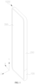
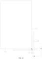
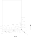
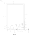
- FIG. 1 is a schematic structural diagram of an electronic device 1000 provided in embodiments of the present disclosure
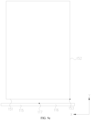
- FIG. 2 is an exploded schematic structural diagram of the electronic device 1000 in FIG. 1
- the electronic device 1000 includes an antenna assembly 100, and a housing 200 and a display screen 300 that cover and are connected to each other.
- An accommodating space is defined between the display screen 300 and the housing 200, and the antenna assembly 100 is disposed in or out of the accommodating space.
- the electronic device 1000 further includes a circuit board 400, a battery 500, a camera, a microphone, a telephone receiver, a loudspeaker, a face recognition module, a fingerprint recognition module, and other components that are disposed in the accommodating space and capable of implementing basic functions of the mobile phone, which will not be repeated in the embodiments.
- the form of the electronic device 1000 is not limited in the present disclosure. Specifically, the electronic device 1000 may be non-deformable, retractable, bendable, foldable, or the like.
- the antenna assembly 100 is disposed on a retractable assembly of the electronic device 1000.
- At least part of the antenna assembly 100 can extend out of the electronic device 1000 along with the retractable assembly of the electronic device 1000, and retract into the electronic device 1000 along with the retractable assembly, so as to increase the clearance space of the radiator and further improve the antenna efficiency when the at least part of the antenna assembly 100 extends out of the electronic device 1000, and to increase the portability of the electronic device 1000 when the at least part of the antenna assembly 100 retracts into the electronic device 1000; or the overall length of the antenna assembly 100 extends along with the extension of the retractable assembly of the electronic device 1000.
- the extension of the length of the antenna assembly 100 includes, but is not limited to, splicing of multiple segments of radiators to form a relatively long length; or the extension of the length of the antenna assembly 100 may also be extension of a distance between the radiator and a radio frequency (RF) chip or other electronic components, so as to increase the clearance space of the antenna assembly 100, thereby further improving the antenna efficiency.
- RF radio frequency
- the antenna assembly 100 is disposed in the accommodating space of the electronic device 1000, or part of the antenna assembly 100 is integrated with the housing 200, or part of the antenna assembly 100 is disposed out of the housing 200.
- the electronic device 1000 introduced above is only one description of the electronic device 1000 for which the antenna assembly 100 is used, and a specific structure of the electronic device 1000 should not be understood as a limitation to the antenna assembly 100 provided in the present disclosure.
- the antenna assembly 100 in the present disclosure includes at least a RF transceiver chip 101, a matching module 102, and a radiator 103.
- the RF transceiver chip 101 may be disposed on the circuit board 400 and electrically connected to the battery 500 or a power management chip, so that the battery 500 supplies power to the RF transceiver chip 101.
- the matching module 102 may be disposed on the circuit board 400 together with the RF transceiver chip 101, or be disposed on another circuit board 400 together with the radiator 103.
- the radiator 103 may be disposed on a support in the accommodating space, or disposed on a surface of the housing 200, or integrated with the housing 200. Specific examples will be provided later.
- the antenna assembly 100 provided in the present disclosure includes, but is not limited to, the following embodiments.
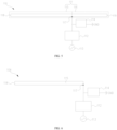
- the antenna assembly 100 includes at least a first antenna element 110.
- the antenna assembly 100 includes at least a first antenna element 110 and a second antenna element 120.
- the antenna assembly 100 may only include a first antenna element 110.
- the first antenna element 110 includes at least a first radiator 111, a first signal source 113, and a ground branch 114.
- the first radiator 111 includes a first radiating branch 115 and a second radiating branch 116 that are integrally connected to each other.
- a joint between the first radiating branch 115 and the second radiating branch 116 is a first feed point 117.
- the first radiating branch 115 has a first free end 118 away from the first feed point 117.
- the second radiating branch 116 has a second free end 119 away from the first feed point 117.
- the first radiator 111 has a first free end 118 and a second free end 119 opposite to the first free end 118, and the first feed point 117 disposed between the first free end 118 and the second free end 119.
- Part of the radiator 103 between the first feed point 117 and the first free end 118 is the first radiating branch 115
- part of the radiator 103 between the first feed point 117 and the second free end 119 is the second radiating branch 116.
- a specific position of the first feed point 117 on the first radiator 111 is not limited in the present disclosure.
- the first radiating branch 115 may have the length equal or unequal to the second radiating branch 116, which is not specifically limited in the present disclosure.
- the shape of the first radiator 111 is strip-shaped, and an extension direction of the first radiator 111 may be a straight line, a curved line, a bent line, or the like.
- an extension direction of the first radiator 111 may be a straight line, a curved line, a bent line, or the like.
- the first free end 118 and the second free end 119 are two opposite extremities.
- the first radiator 111 is in a bent strip shape
- the first free end 118 and the second free end 119 are two extremities in extension directions of the first radiator 111.
- the first radiator 111 may also be in the shape of a strip curve, a sheet, a coating, a rod, a film, or the like.
- the above first radiator 111 may be a line with a uniform width on an extension track, or be in a strip shape with a gradually changing width and a different width such as a widened region.
- the first signal source 113 is electrically connected to the first feed point 117, and is configured to supply a RF signal (electromagnetic energy) to the first radiator 111 through the first feed point 117.
- the first antenna element 110 of the antenna assembly 100 further includes a first matching circuit 112.
- the first matching circuit 112 has one end electrically connected to the first feed point 117, and the other end electrically connected to the first signal source 113.
- the first signal source 113 is a RF transceiver chip 101 for transmitting an RF signal (electromagnetic energy), or a feed portion electrically connected to the RF transceiver chip 101 for transmitting the RF signal (electromagnetic energy).
- the first signal source 113 is configured to feed the electromagnetic energy to the first radiating branch 115 and the second radiating branch 116 through the first matching circuit 112.
- the first matching circuit 112 includes at least one of multiple selection branches formed by switch-capacitor-inductor-resistor, a tuning circuit formed by capacitor-inductor-resistor, or a variable capacitor.
- the first matching circuit 112 is configured to tune impedance of a feeder (from the first signal source 113 to the first radiator 111), so that conversion efficiency of a RF signal into an electromagnetic wave signal can be improved, and conversion efficiency of an electromagnetic wave signal received into a RF signal can be improved.
- the ground branch 114 has one end electrically connected to the first feed point 117, and the other end electrically connected to reference ground GND.
- the antenna assembly 100 has the reference ground GND.
- a specific form of the reference ground GND includes, but is not limited to, a metal plate, a metal layer that is formed in a flexible circuit board 400, etc.
- the reference ground GND is a metal alloy plate in a middle frame of the electronic device 1000.
- the other end of the ground branch 114 is electrically connected to the reference ground GND through a conductive member such as a ground spring sheet, solder, and conductive adhesive.
- the antenna assembly 100 does not have any reference ground GND, and the radiator 103 of the antenna assembly 100 is electrically connected to the reference ground GND of the electronic device 1000 directly or through an intermediate conductive connecting member, or electrically connected to the reference ground GND of an electronic component in the electronic device 1000.
- the ground branch 114, the first signal source 113, and the first radiating branch 115 form at least part of a first sub-antenna 104.
- the ground branch 114, the first signal source 113, the first radiating branch 115, and the reference ground GND form the first sub-antenna 104.
- the ground branch 114, the first signal source 113, and the second radiating branch 116 form at least part of a second sub-antenna 105.
- the ground branch 114, the first signal source 113, the second radiating branch 116, and the reference ground GND form the second sub-antenna 105.
- the first antenna element 110 can form the first sub-antenna 104 and the second sub-antenna 105 independent from the first sub-antenna 104.
- a radiator of the first sub-antenna 104 is different from a radiator of the second sub-antenna 105.
- the radiator of the first sub-antenna 104 is a radiating branch formed by the first radiating branch 115
- the radiator of the second sub-antenna 105 is a radiating branch formed by the second radiating branch 116.
- the first sub-antenna 104 and the second sub-antenna 105 share the first signal source 113, the ground branch 114, and the reference ground GND.
- the first signal source 113 is configured to excite the first radiating branch 115 and the second radiating branch 116 to respectively resonate in a first wavelength mode of a first band.
- a range of the first band is not specifically limited in the present disclosure.
- the frequency of the first band is less than or equal to 1 GHz.
- the first wavelength mode includes, but is not limited to, a quarter-wavelength mode, a half-wavelength mode, a three-quarter-wavelength mode, a one-time-wavelength mode, and the like.
- the first sub-antenna 104 is configured to transmit/receive electromagnetic wave signals of a first target band under excitation of the first signal source 113
- the second sub-antenna 105 is configured to transmit/receive electromagnetic wave signals of a second target band under excitation of the first signal source 113, where the first target band at least partially overlaps with the second target band.
- transmitting/receiving an electromagnetic wave signal of a certain band refers to that an antenna has good efficiency in the band.
- a mode factor of the first antenna element 110 in the band is greater than or equal to x, and for example, x is 0.9, 0.95, and so on, which indicates that the first antenna element 110 has relatively high antenna efficiency in the band.
- x is 0.9, 0.95, and so on.
- the first target band and the second target band are the same bands, and for example, the first target band and the second target band each is: 600MHz-1000MHz (the above values are taken as examples and are not limited), therefore, the first sub-antenna 104 and the second sub-antenna 105 each can transmit/receive electromagnetic wave signals of the first target band (or the second target band).
- the first antenna element 110 since the first antenna element 110 can transmit/receive the electromagnetic wave signals of the first target band (or the second target band) through two current paths, radiation efficiency of the first antenna element 110 in the first target band (or the second target band) is improved.
- the first target band is partially the same as the second target band, and for example, the first target band is 500 MHz-1000MHz (the above values are taken as examples and are not limited), and the second target band is 600MHz-1100MHz (the above values are taken as examples and are not limited). Therefore, the first sub-antenna 104 and the second sub-antenna 105 each can transmit/receive electromagnetic wave signals of 600MHz-1000MHz. For the first antenna element 110, since the first antenna element 110 can transmit/receive the electromagnetic wave signals of 600MHz-1000MHz through the two current paths, the radiation efficiency of the first antenna element 110 in 600 MHz-1000 MHz is improved.
- an overlapping band of the first target band and the second target band is defined as the first band.
- the first signal source 113 is configured to excite the first radiating branch 115 and the second radiating branch 116 to respectively resonate in a first wavelength mode of the first band.
- the first sub-antenna 104 and the second sub-antenna 105 each are configured to transmit/receive electromagnetic wave signals of the first band under excitation of the first signal source 113.
- the first antenna element 110 since the first antenna element 110 can transmit/receive the electromagnetic wave signals of the first band through the two current paths (i.e., the first sub-antenna 104 and the second sub-antenna 105), the radiation efficiency of the first antenna element 110 in the first band is improved.
- the first band is a lower band (LB)
- the radiation efficiency of the first antenna element 110 resonating in the LB is improved, so that the first antenna element 110 is a low-frequency antenna and has relatively high radiation efficiency.
- the second radiating branch 116 is formed by extending the first radiating branch 115 at the first feed point 117, and the ground branch 114 is disposed at the first feed point 117.
- a current distribution is formed between each of the first radiating branch 115, the ground branch 114, and the reference ground GND under the excitation of the first signal source 113, so as to transmit/receive the electromagnetic wave signals covering at least the first band.
- a current distribution is formed between each of the second radiating branch 116 and the ground branch 114 and the reference ground GND under the excitation of the first signal source 113, so as to transmit/receive the electromagnetic wave signals covering at least the first band.
- the first antenna element 110 can form the first sub-antenna 104 and the second sub-antenna 105, the first sub-antenna 104 and the second sub-antenna 105 generate, under the excitation of the first signal source 113, two current distributions that are independent from each other, each current distribution can excite to generate electromagnetic wave signals covering at least the first band, and electromagnetic wave signals of the first band that are generated under excitation of the two current distributions can improve the efficiency of the first band, so as to improve the radiation efficiency of the first antenna element 110 resonating in the first band.
- the range of the first band is not specifically limited in the present disclosure.
- the first band may be at least one of a LB, a middle high band (MHB), or an ultra-high band (UHB), according to division of transceiving bands.
- the LB refers to a band with a frequency less than 1000MHz.
- the LB includes, but is not limited to, at least one of a global system for mobile communication (GSM) 900 band (GSM 900: 890MHz-915MHz; and 935MHz-960MHz), GSM 850 band (GSM 850: 824MHz-849MHz; and 869MHz-894MHz), etc.
- GSM global system for mobile communication
- the MHB refers to a band that is a middle high band.
- the MHB is 1000MHz-3000MHz.
- the MHB includes, but is not limited to, at least one of a long-term evolution (LTE) band 3 (B3) (1710MHz-1785 MHz; and 1805-1880MHz), an LTE band 1 (B1) (1920-1980MHz; and 2110MHz-2170MHz), an LTE band 40 (B40) (2330MHz-2400MHz), an LTE band 41 (B41) (2496MHz-2690MHz), etc.
- LTE long-term evolution
- B3 long-term evolution (LTE) band 3
- B1 (1920-1980MHz; and 2110MHz-2170MHz
- LTE band 40 B40
- B41 (2330MHz-2400MHz
- B41 2496MHz-2690MHz
- the UHB is 3000MHz-6000MHz.
- the above are exemplary division methods for the LB, the MHB, and the UHB, but are not limited thereto.
- the second antenna element 120 includes a second radiator 121, a second matching circuit 122, a second signal source 123, and a first radiator 111.
- a coupling slot 127 is defined between the second radiator 121 and the first radiator 111.
- the first radiator 111 is coupled to the second radiator 121 through the coupling slot 127.
- the second matching circuit 122 has one end electrically connected to the second radiator 121, and the other end electrically connected to the second signal source 123.
- the first radiator 111 and the second radiator 121 can be arranged along a straight line or substantially along a straight line (that is, there is a small tolerance in a design process). In other embodiments, the first radiator 111 and the second radiator 121 may also be arranged in a staggered manner in an extension direction, to provide an avoidance space for other components.
- an end portion of the first radiator 111 faces and is spaced apart from an end portion of the second radiator 121 through the coupling slot 127.
- the coupling slot 127 is a slit between the first radiator 111 and the second radiator 121, and for example, the coupling slot 127 has the width of 0.5mm-2mm, but is not limited to this size.
- the first radiator 111 can be in capacitive coupling with the second radiator 121 through the coupling slot 127. In one of the angles, the first radiator 111 and the second radiator 121 can be considered as two parts formed by the radiator 103 being separated by the coupling slot 127.
- the first radiator 111 is in capacitive coupling with the second radiator 121 through the coupling slot 127.
- the "capacitive coupling" means that, an electric field is generated between the first radiator 111 and the second radiator 121, and a signal of the first radiator 111 can be transferred to the second radiator 121 through the electric field, and a signal of the second radiator 121 can be transferred to the first radiator 111 through the electric field, so that the first radiator 111 and the second radiator 121 can realize electrical signal conduction even in a disconnected state.
- the second radiator 121 can generate an electric field under excitation of the second signal source 123, and energy of the electric field can be transferred to the first radiator 111 through the coupling slot 127, so that the first radiator 111 generates an excitation current.
- the first radiator 111 may also be referred to as a parasitic radiator of the second radiator 121.
- the second signal source 123 is configured to excite the second radiator 121 to resonate in a first wavelength mode of a second band, and excite, through the coupling slot 127, the first radiator 111 to resonate in a second wavelength mode of the second band.
- a range of the second band is not specifically limited in the present disclosure, and optionally, the frequency of the second band is greater than 1GHz.
- the first wavelength mode of the second band includes, but is not limited to, a quarter-wavelength mode, a half-wavelength mode, a three-quarter-wavelength mode, a one-time-wavelength mode, and the like.
- the second wavelength mode of the second band includes, but is not limited to, the quarter-wavelength mode, the half-wavelength mode, the three-quarter-wavelength mode, the one-time-wavelength mode, and the like.
- the specific range of the first band and the specific range of the second band are not limited in the present disclosure.
- the first wavelength mode of the second band and the second wavelength mode of the second band are different wavelength modes.
- the ground branch 114 is disposed at the first feed point 117 of the first radiator 111, so that the first antenna element 110 and the reference ground GND form the first sub-antenna 104 and the second sub-antenna 105, the first sub-antenna 104 and the second sub-antenna 105 each can transmit/receive the electromagnetic wave signals of the first band under the excitation of the first signal source 113, and the first radiating branch 115 and the second radiating branch 116 respectively resonate in the first wavelength mode of the first band under the excitation of the first signal source 113. Therefore, efficiency of the first antenna element 110 in the first band is improved, and the radiation efficiency of the antenna assembly 100 is improved.
- the second radiator 121 resonates in the first wavelength mode of the second band under the action of the second signal source 123
- the first radiator 111 resonates in the second wavelength mode of the second band under excitation of the second signal source 123, the second radiator 121, and the coupling slot 127. Therefore, the first radiator 111 of the first antenna element 110 is also multiplexed as the second radiator 121 of the second antenna element 120, the stacking space of the first radiator 111 of the first antenna element 110 and the second radiator 121 of the second antenna element 120 is saved, and the overall volume of the antenna assembly 100 is reduced.
- the antenna assembly 100 can cover more bands or can cover a band with relatively wide width.
- the antenna assembly 100 When the antenna assembly 100 is disposed in the electronic device 1000, since the electronic device 1000 is provide with the antenna assembly 100, there is no need to additionally dispose a component for improving efficiency, and there is no need to reserve a relatively large clearance space at a periphery of the first radiator 111, so that the antenna efficiency can be effectively improved, the number of components can be reduced, and the space is saved.
- the first radiating branch 115 further has a tuning point 131 between the first free end 118 and the first feed point 117
- the second radiating branch 116 further has a tuning point 131 between the second free end 119 and the first feed point 117.
- the first antenna element 110 of the antenna assembly 100 further includes a switching circuit 132, and the switching circuit 132 has one end electrically connected to the tuning point 131, and the other end electrically connected to the reference ground GND. In other words, the switching circuit 132 is electrically connected to the first radiating branch 115 or the second radiating branch 116.
- there are multiple switching circuits 132 and all the multiple switching circuits 132 may be electrically connected to the first radiating branch 115, all the multiple switching circuits 132 may be electrically connected to the second radiating branch 116, or some of the multiple switching circuits 132 may be electrically connected to the first radiating branch 115 and the rest of the multiple switching circuits 132 may be electrically connected to the second radiating branch 116.
- types of components included in the switching circuit 132 are not limited to an antenna switch, a resistor, a capacitor, an inductor, and the like.
- a tuning branch can be formed by one antenna switch and at least one of an inductor, a capacitor, a resistor, etc., and the switching circuit 132 includes multiple different tuning branches, so that impedance of the switching circuit 132 can be effectively switched by conducting different tuning branches or selecting different tuning branches to conduct, thereby adjusting impedance of the radiating branch electrically connected to the switching circuit 132, so as to adjust the shift of the resonant frequency of the resonant mode generated by the radiating branch.
- the switching circuit 132 when the switching circuit 132 is capacitive in the band on which the switching circuit 132 acts, the resonant frequency of the resonant mode affected by the switching circuit 132 moves toward a lower frequency; and when the switching circuit 132 is inductive in the band on which the switching circuit 132 acts, the resonant frequency of the resonant mode affected by the switching circuit 132 moves towards a higher frequency.
- the first radiating branch 115 has relatively high efficiency in the GSM 900 band, by switching switches in the switching circuit 132, an equivalent inductive value of components in the first radiating branch 115 and in the switching circuit 132 is increased, so that the first radiating branch 115 can generate resonance in the GSM 850 band, and the efficiency is relatively high.
- the switching circuit 132 can switch the first radiating branch 115 from covering the GSM 900 band to covering the GSM 850 band, so as to better cover an actual application band.
- the switching circuit 132 can also switch the GSM 900 band to other bands, which is not repeated herein.
- the first radiating branch 115 or the second radiating branch 116 is selectively provided or not provided with the switching circuit 132, or the first radiating branch 115 and the second radiating branch 116 each are provided with the switching circuit 132, but two switching circuits 132 are tuned to have different or the same impedance characteristics, so that the first radiating branch 115 and the second radiating branch 116 have relatively high transceiving efficiency in the same band (e.g., adjusting from that the first radiating branch 115 and the second radiating branch 116 each have high transceiving efficiency in the GSM 900 band to that the first radiating branch 115 and the second radiating branch 116 each have relatively high transceiving efficiency in the GSM 850 band), or the first radiating branch 115 and the second radiating branch 116 have relatively high transceiving efficiency in different bands (e.g., adjusting from that the first radiating branch 115 and the second radiating branch 116 each have relatively high transceiving efficiency in the GSM 900 band to that the first radiating
- the first antenna element 110 When the first radiating branch 115 and the second radiating branch 116 each generate resonance in the same band, the first antenna element 110 has an efficiency enhancing characteristic in the band; and when the first radiating branch 115 and the second radiating branch 116 generate resonance in different bands, the first antenna element 110 can support more bands at the same time, and has wider application.
- the antenna assembly 100 further includes a controller, the switching circuit 132 includes multiple switches, and the controller is electrically connected to the multiple switches in the switching circuit 132 to control the multiple switches in the switching circuit 132 to be on or off, so as to tune the impedance of the switching circuit 132, thereby tuning the resonance of the radiating branch electrically connected to the switching circuit 132.
- a position of the antenna assembly 100 with respect to the reference ground GND is not specifically limited in the present disclosure.
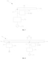
- the reference ground GND includes a first edge 151 and a second edge 152 intersecting the first edge 151, and a connecting point between the first edge 151 and the second edge 152 is a corner portion 153.
- the reference ground GND is substantially rectangular.
- the first radiating branch 115 faces and is spaced apart from the first edge 151
- at least part of the second radiating branch 116 faces and is spaced part from the second edge 152.
- the first radiator 111 is in an L shape.
- the arrangement manner of the first feed point 117 includes, but is not limited to, following cases.
- a first arrangement manner of the first feed point 117 is that the first feed point 117 is opposite to the first edge 151.
- a second arrangement manner of the first feed point 117 is that first feed point 117 is located at one side of the corner portion 153 away from the first edge 151 in an extension direction of the first edge 151.
- a second arrangement manner of the first feed point 117 is that the first feed point 117 is opposite to the second edge 152.
- a fourth arrangement manner of the first feed point 117 is that the first feed point 117 is located at one side of the corner portion 153 away from the second edge 152 in an extension direction of the second edge 152.
- all the first radiator 111 faces the first edge 151, and the first feed point 117 faces the first edge 151.
- all the first radiator 111 faces the second edge 152, and the first feed point 117 faces the second edge 152.
- the extension direction of the first edge 151 of the reference ground GND is defined as an X-axis direction
- the extension direction of the second edge 152 of the reference ground GND is defined as a Y-axis direction
- a thickness direction of the reference ground GND is defined as a Z-axis direction.
- a direction of an arrow is a forward direction
- a direction opposite to the arrow is an opposite direction.
- the first feed point 117 is disposed close to the corner portion 153 of the reference ground GND.
- the first feed point 117 is disposed close to the corner portion 153 of the reference ground GND, more currents in the Y-axis direction can be generated under excitation of the first radiating branch 115 and the second radiating branch 116, and fewer currents in the X-axis direction can be generated under the excitation of the first radiating branch 115 and the second radiating branch 116, so that more longitudinal modes can be excited and fewer transverse modes can be excited, thereby better improving the radiation efficiency.
- the first feed point 117 is located within ⁇ 10 mm of a center, and the center faces the corner portion 153 and is in the extension direction of the first edge 151. This value is only an example, but is not limited thereto.
- the first feed point 117 is located within ⁇ 10 mm of a center, and the center faces the corner portion 153 and is in the extension direction of the second edge 152, and is located in a range of ⁇ 10 mm centered on the corner portion 153.
- This value is only an example, but is not limited thereto.
- FIG. 10 is an equivalent structural diagram of the first radiating branch 115 and the ground branch 114
- FIG. 11 is an equivalent structural diagram of the second radiating branch 116 and the ground branch 114
- the ground branch 114 is equivalent to a small inductor in the first band.
- the ground branch 114 is equivalent to an inductor with inductance less than or equal to 5 nanohenry (nH) in the first band.
- the ground branch 114 which is equivalent to the small inductor, forms a path for the current signal of the first band, so that the current signal corresponding to the first band can be grounded through the ground branch 114.
- Each of the current signal generated on the first radiating branch 115 under the excitation of the first signal source 113 and the current signal generated on the second radiating branch 116 under the excitation of the first signal source 113 can be grounded through the ground branch 114, so that two current paths are formed on the first radiator 111, and in particular, one is grounded from the first radiating branch 115 through the ground branch 114, and the other is grounded from the second radiating branch 116 through the ground branch 114.
- the above two current paths respectively excite the first radiating branch 115 and the second radiating branch 116 to transmit/receive electromagnetic wave signals covering the first band, so that the first antenna element 110 has the relatively high transceiving efficiency in the first band.
- the first band is less than 1000MHz.
- the first sub-antenna 104 and the second sub-antenna 105 each are configured to transmit/receive the electromagnetic wave signals covering the low frequency signal.
- the first band includes at least one of a GSM 900 band or a GSM 850 band.
- the GSM 900 band and the GSM 850 band are bands used by global mobile communication systems in different countries.
- the antenna assembly 100 When the first band covers the GSM 900 band, the antenna assembly 100 has relatively high frequency in the GSM 900 band.
- the antenna assembly 100 When the first band covers the GSM 850 band, the antenna assembly 100 has relatively high frequency in the GSM 850 band.
- the antenna assembly 100 has relatively high frequency in both the GSM 900 band and the GSM 850 band, which will not be illustrated one by one herein.
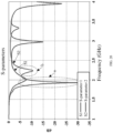
- FIG. 12 is a mode profile of the first sub-antenna 104 illustrated in FIG. 10
- FIG. 13 is a mode profile of the second sub-antenna 105 illustrated in FIG. 11
- characteristic mode analysis is performed on the first sub-antenna 104 illustrated in FIG. 10 and the second sub-antenna 105 illustrated in FIG. 11
- FIG. 12 it can be seen from FIG. 12 that the first sub-antenna 104 generates four radiation modes
- FIG. 13 the second sub-antenna 105 also generates four radiation modes.
- a first radiation mode (corresponding to a curve marked with 1 in FIG.
- the first sub-antenna 104 and a fifth radiation mode (corresponding to a curve marked with 5 in FIG. 13 ) of the second sub-antenna 105 each have a relatively high mode factor (greater than or equal to 0.95) in 0.8GHz-1GHz.
- the mode factor of the first sub-antenna 104 at about 0.915GHz is 0.98
- the mode factor of the second sub-antenna 105 at about 0.915GHz is 0.99.
- a main radiation mode of the first sub-antenna 104 in the GSM 900 band is the first radiation mode
- a main radiation mode of the second sub-antenna 105 in the GSM 900 band is the fifth radiation mode.
- the first sub-antenna 104 and the second sub-antenna 105 each have relatively high radiation efficiency in the GSM 900 band.
- the first radiation mode is a first wavelength mode in which the first radiating branch 115 resonates in the first band.
- the fifth radiation mode is a first wavelength mode in which the second radiating branch 116 resonates in the first band.
- FIG. 14 is a current profile of the first sub-antenna 104 illustrated in FIG. 10 in the first radiation mode
- FIG. 15 is a far-field pattern of the first sub-antenna 104 illustrated in FIG. 10 in the first radiation mode.
- the current of the first sub-antenna 104 flows from the reference ground GND, the ground branch 114, and the first feed point 117 to the first free end 118, and the current forms resonance on the first radiating branch 115, so that the first radiation mode illustrated in FIG. 12 is generated.
- the first radiation mode is a half-wavelength mode of the first radiating branch 115 in the first band, and the mode factor in the first radiation mode is relatively high, so that the first radiation mode is the main radiation mode of the first sub-antenna 104 resonating in the first band.
- the first wavelength mode of the first radiating branch 115 in the first band is a half-wavelength mode.
- the first sub-antenna 104 has a relatively high transceiving efficiency in the first band, and it can be seen from FIG. 15 that the first sub-antenna 104 has a relatively high gain in the first band.
- FIG. 16 is a current profile of the second sub-antenna 105 illustrated in FIG. 11 in the fifth radiation mode
- FIG. 17 is a far-field pattern of the second sub-antenna 105 illustrated in FIG. 11 in the fifth radiation mode.
- the current of the second sub-antenna 105 flows from the reference ground GND, the ground branch 114, and the first feed point 117 to the second free end 119, and the current forms resonance on the second radiating branch 116, so that the fifth radiation mode is generated.
- the fifth radiation mode is a half-wavelength mode of the second radiating branch 116 in the first band, and the mode factor in the fifth radiation mode is relatively high, so that the fifth radiation mode is the main radiation mode of the second sub-antenna 105 resonating in the first band.
- the first wavelength mode of the second radiating branch 116 in the first band is the half-wavelength mode.
- the second sub-antenna 105 has relatively high transceiving efficiency in the first band.
- the first sub-antenna 104 has a relatively high gain in the first band.
- the first radiating branch 115 and the second radiating branch 116 each have the relatively high efficiency in the first band.
- the first radiating branch 115 and the second radiating branch 116 each are part of the first antenna element 110, in other words, two parts of the first antenna element 110 each can have relatively high efficiency in the first band, so that the transceiving efficiency of the first antenna element 110 in the first band is improved.
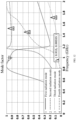
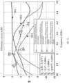
- FIG. 18 is a comparison curve of radiation performance of an antenna assembly provided in embodiments of the present disclosure.
- a dashed line 1 in FIG. 18 is a curve of system efficiency 1 of an antenna assembly 100 provided with a first radiating branch 115, a second radiating branch 116, and a ground branch 114.
- a solid line 1 in FIG. 18 is a curve of the radiation efficiency of the antenna assembly 100 provided with the first radiating branch 115, the second radiating branch 116, and the ground branch 114.
- a dashed line 2 in FIG. 18 is a curve of system efficiency 2 of the antenna assembly 100 without the second radiating branch 116 and the ground branch 114.
- FIG. 18 is a curve of radiation efficiency 2 of the antenna assembly 100 without the second radiating branch 116 and the ground branch 114. It can be seen from FIG. 18 that the antenna assembly 100 provided with the first radiating branch 115, the second radiating branch 116, and the ground branch 114 can significantly improve the radiation performance of the antenna by using an antenna-efficiency-improvement scheme, and the system efficiency is increased by about 2.5dB near 0.92GHz compared to the system efficiency of the antenna assembly 100 without the second radiating branch 116 and the ground branch 114.
- the antenna assembly 100 provided in the present disclosure, corners of the reference ground GND are fully utilized to excite to generate more longitudinal currents, the first radiating branch 115 and the second radiating branch 116 each form an inverted-F antenna (IFA), and the first radiating branch 115 and the second radiating branch 116 each resonate in the half-wavelength mode of the first band under the excitation of the first signal source 113, so that the radiation performance of the antenna assembly 100 is improved during operation.
- IFA inverted-F antenna
- the above is the specific structure of the first antenna element 110, and the first antenna element 110 is provided with the first radiating branch 115, the second radiating branch 116, and the ground branch 114, so that the first radiating branch 115 and the second radiating branch 116 resonate in the same mode, thereby increasing the radiation efficiency of the mode.
- the second radiator 121 has a third free end 124, a ground end 125, and a second feed point 126 between the third free end 124 and the ground end 125.
- the coupling slot 127 is defined between the third free end 124 and an end portion of the first radiator 111.
- the ground end 125 is electrically connected to reference ground GND.
- the second matching circuit 122 has one end electrically connected to the second feed point 126, and the other end electrically connected to the second signal source 123.
- one end of the second antenna element 120 is the third free end 124
- the other end of the second antenna element 120 is the ground end 125
- the second feed point 126 is located between the third free end 124 and the ground end 125, so that the second antenna element 120 is an IFA.
- the length of the second radiator 121 is about a quarter of a free space wavelength of the operating band of the second antenna element 120
- the second antenna element 120 resonates in a fundamental mode state.
- the fundamental mode state is also a quarter-wavelength mode of the antenna, and in this case, the reception conversion efficiency or the transmission conversion efficiency of the antenna is relatively high.
- the first wavelength mode of the second band is a quarter-wavelength mode of the second band.
- the first radiator 111 has the length that is about one time wavelength of the free space wavelength of the operating band of the second antenna element 120.
- the second wavelength mode of the second band is a one-time-wavelength mode of the second band.
- the coupling slot 127 is defined between the third free end 124 and the end portion of the first radiator 111.
- the coupling slot 127 is defined between the third free end 124 and the first free end 118 of the first radiator 111, and the switching circuit 132 of the first antenna element 110 is electrically connected to the first radiating branch 115; or the coupling slot 127 is defined between the third free end 124 and the second free end 119 of the first radiator 111, and the switching circuit 132 of the first antenna element 110 is electrically connected to the second radiating branch 116.
- the second radiator 121 may be disposed at any side of the first radiator 111, and the switching circuit 132 is disposed at one side close to the second radiator 121, so that the switching circuit 132 can tune the operating band of the first antenna element 110 and the operating band of the second antenna element 120.
- the second radiator 121 generates at least one first resonant mode a under excitation of the second signal source 123.
- the first resonant mode a is a first wavelength mode in which the second radiator 121 resonates in the second band.
- the first radiator 111 generates at least one second resonant mode b under excitation of the second signal source 123.
- the second resonant mode b is a second wavelength mode in which the second radiator 121 resonates in the second band.
- the resonant mode is characterized by relatively high transmission efficiency of the electromagnetic wave of the antenna assembly 100 at the resonant frequency of the resonant mode.
- the second radiator 121 has relatively high transceiving efficiency at a certain resonant frequency, under excitation of the second signal source 123, so that transceiving of the electromagnetic wave signal of a band near the resonant frequency can be supported.
- one resonant mode corresponds to one trough curve in FIG. 20
- one resonant mode has one resonant frequency
- the resonant frequency is a frequency corresponding to a trough.
- One resonant mode has a valid band (that is, a band supported by the resonant mode), that is, for example, formed by corresponding frequencies when an absolute value of a return loss less than or equal to a certain value.
- the band supported by the first resonant mode a and the band supported by the second resonant mode b are continuous or discontinuous with each other.
- the multiple bands being continuous means that two adjacent bands supported by the radiator at least partially overlaps, and the multiple bands being discontinuous means that the two adjacent bands supported by the radiator does not overlaps.
- the band supported by the first resonant mode a and the band supported by the second resonant mode b are continuous with each other and form a relatively wide bandwidth, so as to improve data throughput and a data transmission rate of the electronic device 1000 provided with the antenna assembly 100, thereby improving communication quality of the electronic device 1000.
- the bandwidth of the antenna assembly 100 is relatively wide, no tunable component is required to switch different bands, thereby omitting a tunable component, saving costs, and realizing a simple structure of the antenna assembly 100.
- the antenna assembly 100 and the electronic device 1000 provided in the present disclosure by designing the first radiator 111 and the second radiator 121 to be capacitively coupled, multiple resonant modes are generated, so that the antenna assembly 100 can support a relatively wide bandwidth, thereby improving the throughput and data transmission rate of the electronic device 1000 provided with the antenna assembly 100, and improving the communication quality of the electronic device 1000.
- the second radiator 121 when the first radiator 111 is not coupled to the second radiator 121, the second radiator 121 generates one resonance in 1.5GHz-2.5GHz under the excitation of the second signal source 123.
- the first radiator 111 and the second radiator 121 After the first radiator 111 is coupled to the second radiator 121, the first radiator 111 and the second radiator 121 generate two resonances in 1.5GHz-2.5GHz under the excitation of the second signal source 123, where the resonant frequency of the first resonant mode a is about 1.8GHz, and the resonant frequency of the second resonant mode b is about 2.3GHz.
- the second radiator 121 By designing that the first radiator 111 of the first antenna element 110 is in capacitive coupling with the second radiator 121 of the second antenna element 120 through the coupling slot 127, the second radiator 121 generates the first resonant mode a under the excitation of the second signal source 123, and the first radiator 111 generates the second resonant mode b under the excitation of the second signal source 123. Therefore, the number of resonant modes is increased, the bandwidth of the band covered by the second antenna element 120 is further increased, and the bandwidth of transmitting/receiving signals by the antenna assembly 100 is increased.
- the first radiator 111 of the first antenna element 110 can also be used by the first antenna element 110 to generate a resonant mode, thereby broadening a band of the antenna assembly 100.
- a longer second radiator 121 needs to be disposed, so that an overall size of the whole antenna assembly 100 is larger, and in the electronic device 1000 with extremely limited space, the antenna assembly 100 with the relatively large size is not conducive to miniaturization of the electronic device 1000.
- the first resonant mode a and the second resonant mode b are used to support a second band.
- the second band is an MHB of 1GHz-3GHz. Further, the second band covers 1.85GHz-2.35GHz.
- the band covered by the second band includes, but is not limited to, at least one of the B3, the B1, the B40, or the B41.
- the length of the second radiator 121 is about one quarter of the free space wavelength of the operating band of the second antenna element 120, and the second radiator 121 resonates in a quarter-wavelength mode of the second band under the excitation of the second signal source 123, so that the second radiator 121 has relatively high efficiency.
- the first wavelength mode of the second band is the quarter-wavelength mode of the second band.
- the length of the first radiator 111 is about one time of the free space wavelength of the operating band of the second antenna element 120, and the first radiator 111 resonates in a one-time-wavelength mode of the second band under the excitation of the second signal source 123.
- the second wavelength mode of the second band is the one-time-wavelength mode of the second band.
- the antenna assembly 100 provided in the present disclosure utilizes a shared-aperture technology, which utilizes a full-wavelength radiation mode of the radiator of the first antenna element 110 (e.g., a low-frequency antenna), in addition to a quarter-wavelength radiation mode of the own radiator of the second antenna element 120 (e.g., a middle-high-frequency antenna).
- a shared-aperture technology which utilizes a full-wavelength radiation mode of the radiator of the first antenna element 110 (e.g., a low-frequency antenna), in addition to a quarter-wavelength radiation mode of the own radiator of the second antenna element 120 (e.g., a middle-high-frequency antenna).
- performance of the middle-high-frequency antenna is greatly improved compared to a single radiation mode.
- the first antenna element 110 two IFAs are integrated and the two IFAs each are enabled to resonate in the first radiation mode, so that the first antenna element 110 has relatively high efficiency in the first radiation mode, and the antenna assembly 100 has relatively high transceiving efficiency in the LB.
- the switching circuit 32 is disposed on the first radiator 111 to tune the operating band of the first antenna element 110, so that the antenna assembly 100 can effectively cover many bands in the LB, such as the GSM 950 band and the GSM 800 band.
- the first radiator 111 of the first antenna element 110 is coupled to the second radiator 121 of the second antenna element 120, so that the first radiator 111 can also be used for transmitting/receiving in the second band when being used for transmitting/receiving in the first band, and the second band can cover the MHB, such as the B3, the B1, the B40, and the B41, so as to improve the utilization rate of the first radiator 111.
- the bandwidth of the second band is increased, and an overall size of the radiator 103 of the antenna assembly 100 can also be reduced, thereby reducing the overall size of the antenna assembly 100.
- a current distribution corresponding to the first resonant mode a includes, but is not limited to, a first current distribution R1: when the second radiator 121 resonates in the second band, a current is distributed between the ground end 125 and the third free end 124.
- the first current distribution R1 specifically includes, but is not limited to, that the current flows from the ground end 125 to the third free end 124.
- the above current distribution generates the first resonant mode a , that is, the first current distribution on the second radiator 121 corresponds to the quarter-wavelength mode of the second radiator 121 in the second band.
- a current distribution corresponding to the second resonant mode b includes, but is not limited to, a second current distribution R2: when the first radiator 111 resonates in the second band, a current includes a first sub-current R21 and a second sub-current R22.
- the first radiator 111 further has an intersection 133, and the intersection 133 is located between the first free end 118 and the first feed point 117, or between the second free end 119 and the first feed point 117, or at the first feed point 117; and the first sub-current R21 is distributed between the second free end 119 and the intersection 133, the second sub-current R22 is distributed between the first free end 118 and the intersection 133, and the first sub-current R21 has a flow direction opposite to the second sub-current R22.
- the second current distribution R2 specifically includes, but is not limited to, that the first sub-current R21 flows from the second free end 119 to the intersection 133, and the second sub-current R22 flows from the first free end 118 to the intersection 133.
- the intersection 133 includes, but is not limited to, a middle position of the first radiator 111 in an extension-length direction.
- the above current distribution generates the second resonant mode b, that is, the second current distribution of the first radiator 111 corresponds to the one-time-wavelength mode of the first radiator 111 in the second band.
- the current distribution of the second antenna element 120 in the second band is illustrated in FIG. 21 , with arrows representing flow directions of currents and arcs representing range distributions of the currents. It can be seen that on the second radiator 121, the current is distributed according to a quarter wavelength, and on the first radiator 111, the current is distributed according to a one-time wavelength.
- the second antenna element 120 of the antenna assembly 100 resonates in an LTE B1 state.
- FIG. 20 shows a comparison between a reflection coefficient of the second antenna element 120 including the second radiator 121 alone and a reflection coefficient of the second antenna element 120 including the second radiator 121 and the first radiator 111, and it can be found that the second antenna element 120 including the second radiator 121 and the first radiator 111 has a better impedance matching characteristic, and the reflection coefficient is less than -5dB in 1.85GHz-2.35GHz.
- an absolute value of a return loss curve greater than or equal to 5dB is taken as a reference value with relatively high transceiving efficiency of the electromagnetic wave.
- the reference value may also be 6dB, 7dB, and so on.
- the second band covers 1.85GHz-2.35GHz.
- the band covered by the second band includes, but is not limited to, at least one of the B3, the B1, the B40, or the B41.
- FIG. 22 illustrates a comparison between radiation performance of the second antenna element 120 including the second radiator 121 alone and radiation performance of the second antenna element 120 including the second radiator 121 and the first radiator 111, and it can be found that when the second antenna element 120 resonates in B1, the second antenna element 120 including the second radiator 121 and the first radiator 111 has a higher radiation frequency and wider radiation bandwidth, and has peak efficiency 1 dB higher than the efficiency of the second antenna element 120 including the second radiator 121 alone.
- a mean value of system efficiency of the second antenna element 120 including the second radiator 121 and the first radiator 111 is -3dB, and a radiation characteristic is excellent.
- an effective efficiency bandwidth of an antenna is not wide enough, for example, the effective efficiency bandwidth is difficult to cover B3 and B40 at the same time, which causes that switches need to be additionally disposed, resulting in poor signal of the antenna in coverage of certain bands or insufficient miniaturization of the antenna.
- the above bands are merely exemplary, and cannot be taken as a limitation to the bands that can be radiated in the present disclosure.
- the structure of the antenna assembly 100 is miniaturized and multiple resonant modes are generated, and the multiple resonant modes can cover the second band at the same time (e.g., the second band includes 1.85GHz-2.35GHz), so that the antenna assembly 100 can support a relatively wide bandwidth, thereby improving the throughput and the data transmission rate of the electronic device 1000 provided with the antenna assembly 100.
- the antenna assembly 100 is for the above MHB (e.g., 1710MHz-2690MHz)
- B3 and B40 can be supported at the same time. Therefore, the antenna assembly 100 is simple and miniaturized in structure at least, and has relatively high efficiency and data transmission rate in an application band of B3 and B40.
- the bands listed above may be MHBs used by multiple operators, and the antenna assembly 100 provided in the present disclosure may simultaneously support any one or any combination of the multiple bands mentioned above, so that the antenna assembly 100 provided in the present disclosure can support models of the electronic device 1000 corresponding to multiple different operators, and there is no need to adopt different antenna structures for different operators, thereby further improving an application scope of the antenna assembly 100 and compatibility of the antenna assembly 100.
- the present disclosure designs the first antenna element 110 (e.g., the low-frequency antenna) and the second antenna element 120 (e.g., the medium-high-frequency antenna) both with excellent performance, and proposes a set of high-performance terminal antenna solutions.
- the radiation performance of the first antenna element 110 e.g., the low-frequency antenna
- the radiation performance of the first antenna element 110 is greatly improved without increasing additional space and clearance.
- the second antenna element 120 utilizes high-order mode of a metal branch of the first antenna element 110 (for example, a low-frequency antenna) in a shared-aperture manner, and common radiation is formed in the medium-high frequency, thereby greatly improving the radiation performance of the medium-high-frequency antenna.
- the specific position where the radiator 103 of the antenna assembly 100 is disposed on the electronic device 1000 is not specifically limited in the present disclosure.
- the antenna assembly 100 is disposed in the housing 200; or at least part of the antenna assembly 100 is integrated with the housing 200. Specifically, examples are illustrated by the following embodiments.
- the housing 200 includes an edge frame 210 and a rear cover 220.
- a middle plate 230 is formed in the edge frame 210 through injection, and multiple mounting grooves for mounting various electronic components are defined on the middle plate 230.
- the reference ground GND can be located on the middle plate 230.
- the edge frame 210 has one side that surrounds and is connected to the periphery of the rear cover 220, and the other side that surrounds and is connected to the periphery of the display screen 300.
- the edge frame 210 includes multiple side edge-frames connected end to end. Among the multiple side edge-frames of the edge frame 210, two adjacent side edge-frames intersect. For example, the two adjacent side edge-frames are perpendicular to each other.
- the multiple side frames include a top edge-frame 211 and a bottom edge-frame 212 opposite to the top edge-frame 211, and a first side-edge-frame 213 and a second side-edge-frame 214 that each are connected between the top edge-frame 211 and the bottom edge-frame 212.
- Ajoint between two adjacent side edge-frames is a corner 125.
- the top edge-frame 211 is parallel to and equal to the bottom edge-frame 212.
- the first side-edge-frame 213 is parallel to and equal to the second side-edge-frame 214.
- the first side-edge-frame 213 has the length greater than the top edge-frame 211.
- the arrangement of the antenna assembly 100 is not specifically limited in the present disclosure.
- the first radiator 111 of the antenna assembly 100 is disposed at the bottom edge-frame 212, the second side-edge-frame 214, and the corner 125 between the bottom edge-frame 212 and the second side-edge-frame 214.
- the first radiating branch 115 is disposed at the bottom edge-frame 212 close to the second side-edge-frame 214
- the second radiating branch 116 is disposed at the second side-edge-frame 214 close to the bottom edge-frame 212
- the second radiator 121 is disposed at the bottom edge-frame 212 or at the second side-edge-frame 214.
- the first radiator 111 may also be disposed at the top edge-frame 211, the second side-edge-frame 214, and the corner 125 between the top edge-frame 211 and the second side-edge-frame 214.
- the second may be disposed at the top edge-frame 211 or the second side-edge-frame 214.
- the first radiator 111 may also be disposed at other corners 125, which are not listed one by one herein.
- the first radiator 111 is disposed at the corner 125 of the edge frame 210, and the corner 125 of the edge frame 210 corresponds to the corner portion 153 of the reference ground GND, so that the first radiating branch 115 of the first radiator 111 forms an electric field with one edge of the reference ground GND and the second radiating branch 116 of the first radiator 111 forms an electric field with one edge of the reference ground GND, and the first radiating branch 115 and the second radiating branch 116 each can form an IF A with the same construction.
- the first radiating branch 115 and the second radiating branch 116 generate the same radiation mode in the first band, to support transmission/reception of the signal of the first band, thereby improving the transceiving efficiency strengthened of the antenna assembly 100 in the first band can be improved.
- the edge frame 210 is made of metal.
- the first radiator 111, the second radiator 121, and the edge frame 210 are integrated into one body.
- the above radiator 103 may also be integrated with the rear cover 220.
- the first radiator 111 and the second radiator 121 are integrated as part of the housing 200.
- the antenna assembly 100 includes the reference ground GND, the first signal source 113, the second signal source 123, the matching circuit, and the switching circuit 132 that are all disposed on the flexible circuit board 400.
- the first radiator 111 and the second radiator 121 are formed on the surface of the edge frame 210.
- the basic forms of the first radiator 111 and the second radiator 121 include, but are not limited to, a patch radiator 103, or being formed on the inner surface of the edge frame 210 through processes such as laser direct structuring (LDS) or print direct structuring (PDS).
- the edge frame 210 may be made of a non-conductive material.
- the above radiator 103 may also be disposed on the rear cover 220.
- the first radiator 111 and the second radiator 121 are disposed on the flexible printed circuit board 400.
- the flexible printed circuit board 400 is attached to a surface of the edge frame 210.
- the first radiator 111 and the second radiator 121 can be integrated on the flexible printed circuit board 400, and the flexible printed circuit board 400 is attached to the inner surface of the middle frame 240 by an adhesive or the like.
- the edge frame 210 may be made of a non-conductive material.
- the radiator 103 may also be disposed on the inner surface of the rear cover 220.
Abstract
An antenna assembly and an electronic device are provided in the present disclosure. A first antenna element includes a first radiator, a ground branch, and a first signal source. The first radiator includes a first radiating branch and a second radiating branch. A joint of the first radiating branch and the second radiating branch is a first feed point. The ground branch has one end electrically connected to the first feed point, and the other end electrically connected to reference ground. The first signal source is electrically connected to the first feed point, and is configured to excite the first radiating branch and the second radiating branch to respectively resonate in a first wavelength mode of a first band. A second antenna element includes a second radiator, a second signal source, and the first radiator. A coupling slot is defined between the second radiator and the first radiator. The second signal source is electrically connected to the second radiator, and is configured to excite the second radiator to resonate in a first wavelength mode of a second band, and excite, through the coupling slot, the first radiator to resonate in a second wavelength mode of the second band. Antenna efficiency can be improved in the present disclosure.
Description
- This application claims priority to
Chinese Patent Application No. 2021103439701, filed with the Chinese Patent Office on March 30, 2021 - This disclosure relates to the field of communication technology, and specifically to an antenna assembly and an electronic device.
- With more and more functions of electronic devices, the number and types of electronic components in the electronic device are also increased, and people have required the electronic device to be light and thin for portability of the electronic device, so that space reserved for an antenna in the electronic device is more and more limited, and how to improve an antenna structure to have higher antenna efficiency becomes a technical problem to be solved.
- An antenna assembly and an electronic device are provided in the present disclosure, which can improve antenna efficiency.
- An antenna assembly is provided in the present disclosure. The antenna assembly includes a first antenna element and a second antenna element. The first antenna element includes a first radiator, a ground branch, and a first signal source. The first radiator includes a first radiating branch and a second radiating branch that are integrally connected to each other, and a j oint of the first radiating branch and the second radiating branch is a first feed point. The ground branch has one end electrically connected to the first feed point, and the other end electrically connected to reference ground. The first signal source is electrically connected to the first feed point, and the first signal source is configured to excite the first radiating branch and the second radiating branch to respectively resonate in a first wavelength mode of a first band. The second antenna element includes a second radiator, a second signal source, and the first radiator. A coupling slot is defined between the second radiator and the first radiator. The second signal source is electrically connected to the second radiator, and the second signal source is configured to excite the second radiator to resonate in a first wavelength mode of a second band, and excite, through the coupling slot, the first radiator to resonate in a second wavelength mode of the second band.
- An electronic device is provided in the present disclosure. The electronic device includes a housing and an antenna assembly. At least part of the antenna assembly is disposed in the housing, or at least part of the antenna assembly is disposed out of the housing, or at least part of the antenna assembly is integrated with the housing.
- For the antenna assembly and the electronic device provided in the present disclosure, the ground branch is disposed at the feed point of the first radiator, so that the first radiating branch and the second radiating branch respectively resonate in the first wavelength mode of the first band under excitation of the first signal source. Therefore, the first antenna element has relatively high efficiency in the first band, thereby improving radiation performance of the antenna assembly. In addition, the second radiator resonates in the first wavelength mode of the second band under the action of the second signal source, and the first radiator resonates in the second wavelength mode of the second band under excitation of the second signal source, the second radiator, and the coupling slot. Therefore, the radiator of the first antenna element is also multiplexed as the radiator of the second antenna element, the stacking space of the first radiator of the first antenna element and the second radiator of the second antenna element is saved, the overall volume of the antenna assembly is reduced, and the antenna assembly can cover more bands or can cover a band with relatively wide width. When the antenna assembly is disposed in the electronic device, since the electronic device is provided with the antenna assembly, there is no need to additionally dispose a component for improving efficiency, so that the antenna efficiency can be effectively improved, the number of components can be reduced, and the space can be saved.
- To describe the technical solutions in embodiments of the present disclosure more clearly, the following briefly introduces the accompanying drawings required for describing embodiments. Apparently, the accompanying drawings in the following description show merely some embodiments of the present disclosure, and those of ordinary skill in the art may still derive other drawings from these accompanying drawings without creative efforts.
-
FIG. 1 is a schematic structural diagram of an electronic device provided in embodiments of the present disclosure. -
FIG. 2 is an exploded schematic structural diagram of the electronic device provided inFIG. 1 . -
FIG. 3 is a partial schematic structural diagram of the electronic device provided inFIG. 2 . -
FIG. 4 is a schematic structural diagram of an antenna assembly provided inFIG. 3 . -
FIG. 5 is a schematic structural diagram of a first antenna element provided inFIG. 4 . -
FIG. 6 is a schematic structural diagram of a first sub-antenna inFIG. 5 . -
FIG. 7 is a schematic structural diagram of a second sub-antenna inFIG. 5 . -
FIG. 8 is a schematic structural diagram of the first antenna element being provided with a switching circuit inFIG. 5 . -
FIG. 9a is a schematic diagram of the antenna assembly illustrated inFIG. 8 with a first feed point disposed at a first arrangement position. -
FIG. 9b is a schematic diagram of the antenna assembly illustrated inFIG. 8 with a first feed point disposed at a second arrangement position. -
FIG. 9c is a schematic diagram of the antenna assembly illustrated inFIG. 8 with a first feed point disposed at a third arrangement position. -
FIG. 9d is a schematic diagram of the antenna assembly illustrated inFIG. 8 with a first feed point disposed at a fourth arrangement position. -
FIG. 9e is a schematic diagram of the antenna assembly illustrated inFIG. 8 with a first feed point disposed at a fifth arrangement position. -
FIG. 9f is a schematic diagram of the antenna assembly illustrated inFIG. 8 with a first feed point disposed at a sixth arrangement position. -
FIG. 10 is a schematic structural diagram of a first sub-antenna and reference ground illustrated inFIG. 9a . -
FIG. 11 is a schematic structural diagram of a second sub-antenna and reference ground illustrated inFIG. 9a . -
FIG. 12 is a mode profile of the first sub-antenna illustrated inFIG. 10 . -
FIG. 13 is a mode profile of the second sub-antenna illustrated inFIG. 11 . -
FIG. 14 is a current profile of the first sub-antenna illustrated inFIG. 10 in a first radiation mode. -
FIG. 15 is a far-field pattern of the first sub-antenna illustrated inFIG. 10 in a first radiation mode. -
FIG. 16 is a current profile of the second antenna illustrated inFIG. 11 in a fifth radiation mode. -
FIG. 17 is a far-field pattern of the second antenna illustrated inFIG. 11 in a fifth radiation mode. -
FIG. 18 is a comparison curve of radiation performance of an antenna assembly provided in embodiments of the present disclosure. -
FIG. 19 is a schematic structural diagram of the antenna assembly illustrated inFIG. 4 and reference ground. -
FIG. 20 is a graph of S-parameters of the antenna assembly illustrated inFIG. 19 . -
FIG. 21 is a current profile of the antenna assembly illustrated inFIG. 19 under excitation of a second signal source. -
FIG. 22 is a graph of efficiency of the antenna assembly illustrated inFIG. 19 . -
FIG. 23 is a schematic structural diagram of the antenna assembly illustrated inFIG. 21 and a frame that are mounted in a first manner. -
FIG. 24 is a schematic structural diagram of the antenna assembly illustrated inFIG. 21 and a frame that are mounted in a second manner. - The following clearly and completely describes the technical solutions in embodiments of the present disclosure with reference to the accompanying drawings in the embodiments of the present disclosure. Apparently, the described embodiments are merely part rather than all of the embodiments of the present disclosure. In addition, reference herein to "embodiment" or "implementation" means that a particular feature, structure, or characteristic described with reference to the embodiment or the implementation can be included in at least one embodiment of the present disclosure. The appearances of this phrase in various places in the specification are not necessarily all referring to the same embodiment, nor are separate or alternative embodiments mutually exclusive of other embodiments. It is apparent and implicitly understood by those skilled in the art that the embodiments described herein can be combined with other embodiments.
- With development of an electronic device such as a smart phone, the electronic device not only serves as a communication device, but also serves as a multimedia device with rich functions (for example, call, video, camera, and the like). With the increase of the number of electronic components in the electronic device and the pursuit of people on portability of the electronic device, the space reserved for an antenna in the electronic device has become smaller and smaller. For example, in 5th generation (5G) mobile communication at present, due to full screen configuration of the electronic device, the clearance space reserved for the antenna is smaller, which greatly affects efficiency of the antenna for receiving an electromagnetic wave and transmitting an electromagnetic wave. At present, a research direction is mainly to reduce an impact of components around the antenna (such as a speaker box, a universal serial bus (USB) data port, a camera, and the like) on the performance of the antenna. However, as the space in the mobile phone reserved for the antenna becomes more and more limited, it is not enough to research this direction alone. Therefore, how to improve an antenna structure and improve antenna efficiency becomes a technical problem to be solved.
- For an antenna assembly provided in embodiments of the present disclosure, an antenna structure is improved, and antenna efficiency (the antenna efficiency refers to reception conversion efficiency and transmission conversion efficiency of the antenna assembly for an electromagnetic wave, which will not be described hereinafter) is improved, so that the antenna assembly can be effectively used for a present electronic device with multiple functions and a full screen. The product type of the electronic device for which an antenna assembly is used is not specifically limited in the present disclosure. The electronic device includes, but is not limited to, devices capable of transmitting/receiving electromagnetic wave signals, such as a telephone, a television, a tablet computer, a smart phone, a camera, a personal computer, a notebook computer, an on-board device, an earphone, a watch, a wearable device, a base station, an on-board radar, and a customer premise equipment (CPE). In the present disclosure, for illustrative purpose, the electronic device is a smart phone, and other devices may refer to the detailed description in the present disclosure.
- Reference is made to
FIG. 1 andFIG. 2 , whereFIG. 1 is a schematic structural diagram of anelectronic device 1000 provided in embodiments of the present disclosure, andFIG. 2 is an exploded schematic structural diagram of theelectronic device 1000 inFIG. 1 . Theelectronic device 1000 includes anantenna assembly 100, and ahousing 200 and adisplay screen 300 that cover and are connected to each other. An accommodating space is defined between thedisplay screen 300 and thehousing 200, and theantenna assembly 100 is disposed in or out of the accommodating space. Theelectronic device 1000 further includes acircuit board 400, abattery 500, a camera, a microphone, a telephone receiver, a loudspeaker, a face recognition module, a fingerprint recognition module, and other components that are disposed in the accommodating space and capable of implementing basic functions of the mobile phone, which will not be repeated in the embodiments. - The form of the
electronic device 1000 is not limited in the present disclosure. Specifically, theelectronic device 1000 may be non-deformable, retractable, bendable, foldable, or the like. Optionally, theantenna assembly 100 is disposed on a retractable assembly of theelectronic device 1000. In other words, at least part of theantenna assembly 100 can extend out of theelectronic device 1000 along with the retractable assembly of theelectronic device 1000, and retract into theelectronic device 1000 along with the retractable assembly, so as to increase the clearance space of the radiator and further improve the antenna efficiency when the at least part of theantenna assembly 100 extends out of theelectronic device 1000, and to increase the portability of theelectronic device 1000 when the at least part of theantenna assembly 100 retracts into theelectronic device 1000; or the overall length of theantenna assembly 100 extends along with the extension of the retractable assembly of theelectronic device 1000. Optionally, the extension of the length of theantenna assembly 100 includes, but is not limited to, splicing of multiple segments of radiators to form a relatively long length; or the extension of the length of theantenna assembly 100 may also be extension of a distance between the radiator and a radio frequency (RF) chip or other electronic components, so as to increase the clearance space of theantenna assembly 100, thereby further improving the antenna efficiency. - Optionally, the
antenna assembly 100 is disposed in the accommodating space of theelectronic device 1000, or part of theantenna assembly 100 is integrated with thehousing 200, or part of theantenna assembly 100 is disposed out of thehousing 200. It can be understood that theelectronic device 1000 introduced above is only one description of theelectronic device 1000 for which theantenna assembly 100 is used, and a specific structure of theelectronic device 1000 should not be understood as a limitation to theantenna assembly 100 provided in the present disclosure. - Referring to
FIG. 3 , theantenna assembly 100 in the present disclosure includes at least aRF transceiver chip 101, amatching module 102, and aradiator 103. TheRF transceiver chip 101 may be disposed on thecircuit board 400 and electrically connected to thebattery 500 or a power management chip, so that thebattery 500 supplies power to theRF transceiver chip 101. Thematching module 102 may be disposed on thecircuit board 400 together with theRF transceiver chip 101, or be disposed on anothercircuit board 400 together with theradiator 103. Theradiator 103 may be disposed on a support in the accommodating space, or disposed on a surface of thehousing 200, or integrated with thehousing 200. Specific examples will be provided later. - A structure of the
antenna assembly 100 provided in the present disclosure will be specifically described in detail below with reference to the accompanying drawings. Theantenna assembly 100 provided in the present disclosure includes, but is not limited to, the following embodiments. - Referring to
FIG. 4 , theantenna assembly 100 includes at least afirst antenna element 110. In this embodiment, theantenna assembly 100 includes at least afirst antenna element 110 and asecond antenna element 120. - Referring to
FIG. 5 , theantenna assembly 100 may only include afirst antenna element 110. Thefirst antenna element 110 includes at least afirst radiator 111, afirst signal source 113, and aground branch 114. - Referring to
FIG. 5 , thefirst radiator 111 includes afirst radiating branch 115 and asecond radiating branch 116 that are integrally connected to each other. A joint between thefirst radiating branch 115 and thesecond radiating branch 116 is afirst feed point 117. - Referring to
FIG. 5 , thefirst radiating branch 115 has a firstfree end 118 away from thefirst feed point 117. Thesecond radiating branch 116 has a secondfree end 119 away from thefirst feed point 117. In other words, thefirst radiator 111 has a firstfree end 118 and a secondfree end 119 opposite to the firstfree end 118, and thefirst feed point 117 disposed between the firstfree end 118 and the secondfree end 119. Part of theradiator 103 between thefirst feed point 117 and the firstfree end 118 is thefirst radiating branch 115, and part of theradiator 103 between thefirst feed point 117 and the secondfree end 119 is thesecond radiating branch 116. A specific position of thefirst feed point 117 on thefirst radiator 111 is not limited in the present disclosure. In other words, thefirst radiating branch 115 may have the length equal or unequal to thesecond radiating branch 116, which is not specifically limited in the present disclosure. - Optionally, the shape of the
first radiator 111 is strip-shaped, and an extension direction of thefirst radiator 111 may be a straight line, a curved line, a bent line, or the like. When thefirst radiator 111 is in a linear strip shape, the firstfree end 118 and the secondfree end 119 are two opposite extremities. When thefirst radiator 111 is in a bent strip shape, the firstfree end 118 and the secondfree end 119 are two extremities in extension directions of thefirst radiator 111. In other embodiments, thefirst radiator 111 may also be in the shape of a strip curve, a sheet, a coating, a rod, a film, or the like. The abovefirst radiator 111 may be a line with a uniform width on an extension track, or be in a strip shape with a gradually changing width and a different width such as a widened region. - Referring to
FIG. 5 , thefirst signal source 113 is electrically connected to thefirst feed point 117, and is configured to supply a RF signal (electromagnetic energy) to thefirst radiator 111 through thefirst feed point 117. - Optionally, referring to
FIG. 5 , thefirst antenna element 110 of theantenna assembly 100 further includes afirst matching circuit 112. Thefirst matching circuit 112 has one end electrically connected to thefirst feed point 117, and the other end electrically connected to thefirst signal source 113. Thefirst signal source 113 is aRF transceiver chip 101 for transmitting an RF signal (electromagnetic energy), or a feed portion electrically connected to theRF transceiver chip 101 for transmitting the RF signal (electromagnetic energy). Thefirst signal source 113 is configured to feed the electromagnetic energy to thefirst radiating branch 115 and thesecond radiating branch 116 through thefirst matching circuit 112. Optionally, thefirst matching circuit 112 includes at least one of multiple selection branches formed by switch-capacitor-inductor-resistor, a tuning circuit formed by capacitor-inductor-resistor, or a variable capacitor. Thefirst matching circuit 112 is configured to tune impedance of a feeder (from thefirst signal source 113 to the first radiator 111), so that conversion efficiency of a RF signal into an electromagnetic wave signal can be improved, and conversion efficiency of an electromagnetic wave signal received into a RF signal can be improved. - Optionally, the
ground branch 114 has one end electrically connected to thefirst feed point 117, and the other end electrically connected to reference ground GND. Optionally, theantenna assembly 100 has the reference ground GND. A specific form of the reference ground GND includes, but is not limited to, a metal plate, a metal layer that is formed in aflexible circuit board 400, etc. When theantenna assembly 100 is disposed in theelectronic device 1000, the reference ground GND is a metal alloy plate in a middle frame of theelectronic device 1000. The other end of theground branch 114 is electrically connected to the reference ground GND through a conductive member such as a ground spring sheet, solder, and conductive adhesive. In other embodiments, theantenna assembly 100 does not have any reference ground GND, and theradiator 103 of theantenna assembly 100 is electrically connected to the reference ground GND of theelectronic device 1000 directly or through an intermediate conductive connecting member, or electrically connected to the reference ground GND of an electronic component in theelectronic device 1000. - Optionally, referring to
FIG. 6 , theground branch 114, thefirst signal source 113, and thefirst radiating branch 115 form at least part of afirst sub-antenna 104. Specifically, theground branch 114, thefirst signal source 113, thefirst radiating branch 115, and the reference ground GND form thefirst sub-antenna 104. - Optionally, referring to
FIG. 7 , theground branch 114, thefirst signal source 113, and thesecond radiating branch 116 form at least part of asecond sub-antenna 105. Specifically, theground branch 114, thefirst signal source 113, thesecond radiating branch 116, and the reference ground GND form thesecond sub-antenna 105. - Thus, the
first antenna element 110 can form thefirst sub-antenna 104 and thesecond sub-antenna 105 independent from thefirst sub-antenna 104. A radiator of thefirst sub-antenna 104 is different from a radiator of thesecond sub-antenna 105. Specifically, the radiator of thefirst sub-antenna 104 is a radiating branch formed by thefirst radiating branch 115, and the radiator of thesecond sub-antenna 105 is a radiating branch formed by thesecond radiating branch 116. Thefirst sub-antenna 104 and thesecond sub-antenna 105 share thefirst signal source 113, theground branch 114, and the reference ground GND. - The
first signal source 113 is configured to excite thefirst radiating branch 115 and thesecond radiating branch 116 to respectively resonate in a first wavelength mode of a first band. A range of the first band is not specifically limited in the present disclosure. Optionally, the frequency of the first band is less than or equal to 1 GHz. The first wavelength mode includes, but is not limited to, a quarter-wavelength mode, a half-wavelength mode, a three-quarter-wavelength mode, a one-time-wavelength mode, and the like. - Specifically, the
first sub-antenna 104 is configured to transmit/receive electromagnetic wave signals of a first target band under excitation of thefirst signal source 113, and thesecond sub-antenna 105 is configured to transmit/receive electromagnetic wave signals of a second target band under excitation of thefirst signal source 113, where the first target band at least partially overlaps with the second target band. It can be understood that in the present disclosure, transmitting/receiving an electromagnetic wave signal of a certain band refers to that an antenna has good efficiency in the band. For example, based on characteristic mode analysis, a mode factor of thefirst antenna element 110 in the band is greater than or equal to x, and for example, x is 0.9, 0.95, and so on, which indicates that thefirst antenna element 110 has relatively high antenna efficiency in the band. The above values are only examples, and are not limited thereto. - Optionally, the first target band and the second target band are the same bands, and for example, the first target band and the second target band each is: 600MHz-1000MHz (the above values are taken as examples and are not limited), therefore, the
first sub-antenna 104 and thesecond sub-antenna 105 each can transmit/receive electromagnetic wave signals of the first target band (or the second target band). For thefirst antenna element 110, since thefirst antenna element 110 can transmit/receive the electromagnetic wave signals of the first target band (or the second target band) through two current paths, radiation efficiency of thefirst antenna element 110 in the first target band (or the second target band) is improved. - Optionally, the first target band is partially the same as the second target band, and for example, the first target band is 500 MHz-1000MHz (the above values are taken as examples and are not limited), and the second target band is 600MHz-1100MHz (the above values are taken as examples and are not limited). Therefore, the
first sub-antenna 104 and thesecond sub-antenna 105 each can transmit/receive electromagnetic wave signals of 600MHz-1000MHz. For thefirst antenna element 110, since thefirst antenna element 110 can transmit/receive the electromagnetic wave signals of 600MHz-1000MHz through the two current paths, the radiation efficiency of thefirst antenna element 110 in 600 MHz-1000 MHz is improved. - Regardless of whether the first target band is partially or completely the same as the second target band, in this embodiment, an overlapping band of the first target band and the second target band is defined as the first band. In other words, the
first signal source 113 is configured to excite thefirst radiating branch 115 and thesecond radiating branch 116 to respectively resonate in a first wavelength mode of the first band. Thefirst sub-antenna 104 and thesecond sub-antenna 105 each are configured to transmit/receive electromagnetic wave signals of the first band under excitation of thefirst signal source 113. For thefirst antenna element 110, since thefirst antenna element 110 can transmit/receive the electromagnetic wave signals of the first band through the two current paths (i.e., thefirst sub-antenna 104 and the second sub-antenna 105), the radiation efficiency of thefirst antenna element 110 in the first band is improved. When the first band is a lower band (LB), the radiation efficiency of thefirst antenna element 110 resonating in the LB is improved, so that thefirst antenna element 110 is a low-frequency antenna and has relatively high radiation efficiency. - In the present disclosure, the structure of the
antenna assembly 100 is improved. Thesecond radiating branch 116 is formed by extending thefirst radiating branch 115 at thefirst feed point 117, and theground branch 114 is disposed at thefirst feed point 117. A current distribution is formed between each of thefirst radiating branch 115, theground branch 114, and the reference ground GND under the excitation of thefirst signal source 113, so as to transmit/receive the electromagnetic wave signals covering at least the first band. A current distribution is formed between each of thesecond radiating branch 116 and theground branch 114 and the reference ground GND under the excitation of thefirst signal source 113, so as to transmit/receive the electromagnetic wave signals covering at least the first band. Therefore, thefirst antenna element 110 can form thefirst sub-antenna 104 and thesecond sub-antenna 105, thefirst sub-antenna 104 and thesecond sub-antenna 105 generate, under the excitation of thefirst signal source 113, two current distributions that are independent from each other, each current distribution can excite to generate electromagnetic wave signals covering at least the first band, and electromagnetic wave signals of the first band that are generated under excitation of the two current distributions can improve the efficiency of the first band, so as to improve the radiation efficiency of thefirst antenna element 110 resonating in the first band. - The range of the first band is not specifically limited in the present disclosure. For example, the first band may be at least one of a LB, a middle high band (MHB), or an ultra-high band (UHB), according to division of transceiving bands. The LB refers to a band with a frequency less than 1000MHz. The LB includes, but is not limited to, at least one of a global system for mobile communication (GSM) 900 band (GSM 900: 890MHz-915MHz; and 935MHz-960MHz), GSM 850 band (GSM 850: 824MHz-849MHz; and 869MHz-894MHz), etc. The MHB refers to a band that is a middle high band. The MHB is 1000MHz-3000MHz. The MHB includes, but is not limited to, at least one of a long-term evolution (LTE) band 3 (B3) (1710MHz-1785 MHz; and 1805-1880MHz), an LTE band 1 (B1) (1920-1980MHz; and 2110MHz-2170MHz), an LTE band 40 (B40) (2330MHz-2400MHz), an LTE band 41 (B41) (2496MHz-2690MHz), etc. The UHB is 3000MHz-6000MHz. The above are exemplary division methods for the LB, the MHB, and the UHB, but are not limited thereto.
- Optionally, referring to
FIG. 4 , thesecond antenna element 120 includes asecond radiator 121, asecond matching circuit 122, asecond signal source 123, and afirst radiator 111. Acoupling slot 127 is defined between thesecond radiator 121 and thefirst radiator 111. Thefirst radiator 111 is coupled to thesecond radiator 121 through thecoupling slot 127. Thesecond matching circuit 122 has one end electrically connected to thesecond radiator 121, and the other end electrically connected to thesecond signal source 123. - Referring to
FIG. 4 , thefirst radiator 111 and thesecond radiator 121 can be arranged along a straight line or substantially along a straight line (that is, there is a small tolerance in a design process). In other embodiments, thefirst radiator 111 and thesecond radiator 121 may also be arranged in a staggered manner in an extension direction, to provide an avoidance space for other components. - Referring to
FIG. 4 , an end portion of thefirst radiator 111 faces and is spaced apart from an end portion of thesecond radiator 121 through thecoupling slot 127. Optionally, thecoupling slot 127 is a slit between thefirst radiator 111 and thesecond radiator 121, and for example, thecoupling slot 127 has the width of 0.5mm-2mm, but is not limited to this size. Thefirst radiator 111 can be in capacitive coupling with thesecond radiator 121 through thecoupling slot 127. In one of the angles, thefirst radiator 111 and thesecond radiator 121 can be considered as two parts formed by theradiator 103 being separated by thecoupling slot 127. - The
first radiator 111 is in capacitive coupling with thesecond radiator 121 through thecoupling slot 127. The "capacitive coupling" means that, an electric field is generated between thefirst radiator 111 and thesecond radiator 121, and a signal of thefirst radiator 111 can be transferred to thesecond radiator 121 through the electric field, and a signal of thesecond radiator 121 can be transferred to thefirst radiator 111 through the electric field, so that thefirst radiator 111 and thesecond radiator 121 can realize electrical signal conduction even in a disconnected state. In this embodiment, thesecond radiator 121 can generate an electric field under excitation of thesecond signal source 123, and energy of the electric field can be transferred to thefirst radiator 111 through thecoupling slot 127, so that thefirst radiator 111 generates an excitation current. In other words, thefirst radiator 111 may also be referred to as a parasitic radiator of thesecond radiator 121. - The
second signal source 123 is configured to excite thesecond radiator 121 to resonate in a first wavelength mode of a second band, and excite, through thecoupling slot 127, thefirst radiator 111 to resonate in a second wavelength mode of the second band. A range of the second band is not specifically limited in the present disclosure, and optionally, the frequency of the second band is greater than 1GHz. The first wavelength mode of the second band includes, but is not limited to, a quarter-wavelength mode, a half-wavelength mode, a three-quarter-wavelength mode, a one-time-wavelength mode, and the like. The second wavelength mode of the second band includes, but is not limited to, the quarter-wavelength mode, the half-wavelength mode, the three-quarter-wavelength mode, the one-time-wavelength mode, and the like. - The specific range of the first band and the specific range of the second band are not limited in the present disclosure. Optionally, the first wavelength mode of the second band and the second wavelength mode of the second band are different wavelength modes.
- For the
antenna assembly 100 and theelectronic device 1000 provided in the present disclosure, theground branch 114 is disposed at thefirst feed point 117 of thefirst radiator 111, so that thefirst antenna element 110 and the reference ground GND form thefirst sub-antenna 104 and thesecond sub-antenna 105, thefirst sub-antenna 104 and thesecond sub-antenna 105 each can transmit/receive the electromagnetic wave signals of the first band under the excitation of thefirst signal source 113, and thefirst radiating branch 115 and thesecond radiating branch 116 respectively resonate in the first wavelength mode of the first band under the excitation of thefirst signal source 113. Therefore, efficiency of thefirst antenna element 110 in the first band is improved, and the radiation efficiency of theantenna assembly 100 is improved. Thesecond radiator 121 resonates in the first wavelength mode of the second band under the action of thesecond signal source 123, and thefirst radiator 111 resonates in the second wavelength mode of the second band under excitation of thesecond signal source 123, thesecond radiator 121, and thecoupling slot 127. Therefore, thefirst radiator 111 of thefirst antenna element 110 is also multiplexed as thesecond radiator 121 of thesecond antenna element 120, the stacking space of thefirst radiator 111 of thefirst antenna element 110 and thesecond radiator 121 of thesecond antenna element 120 is saved, and the overall volume of theantenna assembly 100 is reduced. In addition, theantenna assembly 100 can cover more bands or can cover a band with relatively wide width. - When the
antenna assembly 100 is disposed in theelectronic device 1000, since theelectronic device 1000 is provide with theantenna assembly 100, there is no need to additionally dispose a component for improving efficiency, and there is no need to reserve a relatively large clearance space at a periphery of thefirst radiator 111, so that the antenna efficiency can be effectively improved, the number of components can be reduced, and the space is saved. - Optionally, referring to
FIG. 8 , thefirst radiating branch 115 further has atuning point 131 between the firstfree end 118 and thefirst feed point 117, or thesecond radiating branch 116 further has atuning point 131 between the secondfree end 119 and thefirst feed point 117. Thefirst antenna element 110 of theantenna assembly 100 further includes aswitching circuit 132, and theswitching circuit 132 has one end electrically connected to thetuning point 131, and the other end electrically connected to the reference ground GND. In other words, theswitching circuit 132 is electrically connected to thefirst radiating branch 115 or thesecond radiating branch 116. In other embodiments, there are multiple switchingcircuits 132, and all themultiple switching circuits 132 may be electrically connected to thefirst radiating branch 115, all themultiple switching circuits 132 may be electrically connected to thesecond radiating branch 116, or some of themultiple switching circuits 132 may be electrically connected to thefirst radiating branch 115 and the rest of themultiple switching circuits 132 may be electrically connected to thesecond radiating branch 116. - Optionally, types of components included in the
switching circuit 132 are not limited to an antenna switch, a resistor, a capacitor, an inductor, and the like. A tuning branch can be formed by one antenna switch and at least one of an inductor, a capacitor, a resistor, etc., and theswitching circuit 132 includes multiple different tuning branches, so that impedance of theswitching circuit 132 can be effectively switched by conducting different tuning branches or selecting different tuning branches to conduct, thereby adjusting impedance of the radiating branch electrically connected to theswitching circuit 132, so as to adjust the shift of the resonant frequency of the resonant mode generated by the radiating branch. For example, when theswitching circuit 132 is capacitive in the band on which theswitching circuit 132 acts, the resonant frequency of the resonant mode affected by the switchingcircuit 132 moves toward a lower frequency; and when theswitching circuit 132 is inductive in the band on which theswitching circuit 132 acts, the resonant frequency of the resonant mode affected by the switchingcircuit 132 moves towards a higher frequency. In addition, for example, when thefirst radiating branch 115 has relatively high efficiency in the GSM 900 band, by switching switches in theswitching circuit 132, an equivalent inductive value of components in thefirst radiating branch 115 and in theswitching circuit 132 is increased, so that thefirst radiating branch 115 can generate resonance in the GSM 850 band, and the efficiency is relatively high. Therefore, theswitching circuit 132 can switch thefirst radiating branch 115 from covering the GSM 900 band to covering the GSM 850 band, so as to better cover an actual application band. Theswitching circuit 132 can also switch the GSM 900 band to other bands, which is not repeated herein. - Optionally, the
first radiating branch 115 or thesecond radiating branch 116 is selectively provided or not provided with theswitching circuit 132, or thefirst radiating branch 115 and thesecond radiating branch 116 each are provided with theswitching circuit 132, but two switchingcircuits 132 are tuned to have different or the same impedance characteristics, so that thefirst radiating branch 115 and thesecond radiating branch 116 have relatively high transceiving efficiency in the same band (e.g., adjusting from that thefirst radiating branch 115 and thesecond radiating branch 116 each have high transceiving efficiency in the GSM 900 band to that thefirst radiating branch 115 and thesecond radiating branch 116 each have relatively high transceiving efficiency in the GSM 850 band), or thefirst radiating branch 115 and thesecond radiating branch 116 have relatively high transceiving efficiency in different bands (e.g., adjusting from that thefirst radiating branch 115 and thesecond radiating branch 116 each have relatively high transceiving efficiency in the GSM 900 band to that thefirst radiating branch 115 has relatively high transceiving efficiency in the GSM 900 band and thesecond radiating branch 116 has relatively high transceiving efficiency in the GSM 850 band). When thefirst radiating branch 115 and thesecond radiating branch 116 each generate resonance in the same band, thefirst antenna element 110 has an efficiency enhancing characteristic in the band; and when thefirst radiating branch 115 and thesecond radiating branch 116 generate resonance in different bands, thefirst antenna element 110 can support more bands at the same time, and has wider application. - Optionally, the
antenna assembly 100 further includes a controller, theswitching circuit 132 includes multiple switches, and the controller is electrically connected to the multiple switches in theswitching circuit 132 to control the multiple switches in theswitching circuit 132 to be on or off, so as to tune the impedance of theswitching circuit 132, thereby tuning the resonance of the radiating branch electrically connected to theswitching circuit 132. - A position of the
antenna assembly 100 with respect to the reference ground GND is not specifically limited in the present disclosure. - Referring to
FIG. 9a , the reference ground GND includes afirst edge 151 and asecond edge 152 intersecting thefirst edge 151, and a connecting point between thefirst edge 151 and thesecond edge 152 is acorner portion 153. For example, the reference ground GND is substantially rectangular. - Optionally, at least part of the
first radiating branch 115 faces and is spaced apart from thefirst edge 151, and at least part of thesecond radiating branch 116 faces and is spaced part from thesecond edge 152. In other words, thefirst radiator 111 is in an L shape. In this embodiment, the arrangement manner of thefirst feed point 117 includes, but is not limited to, following cases. - Referring to
FIG. 9a , a first arrangement manner of thefirst feed point 117 is that thefirst feed point 117 is opposite to thefirst edge 151. - Referring to
FIG. 9b , a second arrangement manner of thefirst feed point 117 is thatfirst feed point 117 is located at one side of thecorner portion 153 away from thefirst edge 151 in an extension direction of thefirst edge 151. - Referring to
FIG. 9c , a second arrangement manner of thefirst feed point 117 is that thefirst feed point 117 is opposite to thesecond edge 152. - Referring to
FIG. 9d , a fourth arrangement manner of thefirst feed point 117 is that thefirst feed point 117 is located at one side of thecorner portion 153 away from thesecond edge 152 in an extension direction of thesecond edge 152. - Optionally, referring to
FIG. 9e , all thefirst radiator 111 faces thefirst edge 151, and thefirst feed point 117 faces thefirst edge 151. - Optionally, referring to
FIG. 9f , all thefirst radiator 111 faces thesecond edge 152, and thefirst feed point 117 faces thesecond edge 152. - For convenience of description, the extension direction of the
first edge 151 of the reference ground GND is defined as an X-axis direction, the extension direction of thesecond edge 152 of the reference ground GND is defined as a Y-axis direction, and a thickness direction of the reference ground GND is defined as a Z-axis direction. A direction of an arrow is a forward direction, and a direction opposite to the arrow is an opposite direction. - Referring to
FIG. 9a , optionally, thefirst feed point 117 is disposed close to thecorner portion 153 of the reference ground GND. Thefirst feed point 117 is disposed close to thecorner portion 153 of the reference ground GND, more currents in the Y-axis direction can be generated under excitation of thefirst radiating branch 115 and thesecond radiating branch 116, and fewer currents in the X-axis direction can be generated under the excitation of thefirst radiating branch 115 and thesecond radiating branch 116, so that more longitudinal modes can be excited and fewer transverse modes can be excited, thereby better improving the radiation efficiency. It can be understood that when thefirst feed point 117 is closer to thecorner portion 153 of the reference ground GND, more currents in the Y-axis direction can be generated under the excitation of thefirst radiator 111, and therefore the resonance current has more longitudinal modes, and the antenna efficiency can be improved better. - Specifically, the
first feed point 117 is located within ±10 mm of a center, and the center faces thecorner portion 153 and is in the extension direction of thefirst edge 151. This value is only an example, but is not limited thereto. - Specifically, the
first feed point 117 is located within ±10 mm of a center, and the center faces thecorner portion 153 and is in the extension direction of thesecond edge 152, and is located in a range of ±10 mm centered on thecorner portion 153. This value is only an example, but is not limited thereto. - Reference is made to
FIG. 10 andFIG. 11 , whereFIG. 10 is an equivalent structural diagram of thefirst radiating branch 115 and theground branch 114, andFIG. 11 is an equivalent structural diagram of thesecond radiating branch 116 and theground branch 114. Theground branch 114 is equivalent to a small inductor in the first band. Optionally, theground branch 114 is equivalent to an inductor with inductance less than or equal to 5 nanohenry (nH) in the first band. Theground branch 114, which is equivalent to the small inductor, forms a path for the current signal of the first band, so that the current signal corresponding to the first band can be grounded through theground branch 114. Each of the current signal generated on thefirst radiating branch 115 under the excitation of thefirst signal source 113 and the current signal generated on thesecond radiating branch 116 under the excitation of thefirst signal source 113 can be grounded through theground branch 114, so that two current paths are formed on thefirst radiator 111, and in particular, one is grounded from thefirst radiating branch 115 through theground branch 114, and the other is grounded from thesecond radiating branch 116 through theground branch 114. The above two current paths respectively excite thefirst radiating branch 115 and thesecond radiating branch 116 to transmit/receive electromagnetic wave signals covering the first band, so that thefirst antenna element 110 has the relatively high transceiving efficiency in the first band. Optionally, the first band is less than 1000MHz. In other words, thefirst sub-antenna 104 and thesecond sub-antenna 105 each are configured to transmit/receive the electromagnetic wave signals covering the low frequency signal. - Optionally, the first band includes at least one of a GSM 900 band or a GSM 850 band. The GSM 900 band and the GSM 850 band are bands used by global mobile communication systems in different countries. When the first band covers the GSM 900 band, the
antenna assembly 100 has relatively high frequency in the GSM 900 band. When the first band covers the GSM 850 band, theantenna assembly 100 has relatively high frequency in the GSM 850 band. When the first band covers both the GSM 900 band and the GSM 850 band, theantenna assembly 100 has relatively high frequency in both the GSM 900 band and the GSM 850 band, which will not be illustrated one by one herein. - Reference is made to
FIG. 12 andFIG. 13 , whereFIG. 12 is a mode profile of thefirst sub-antenna 104 illustrated inFIG. 10 , andFIG. 13 is a mode profile of thesecond sub-antenna 105 illustrated inFIG. 11 . After characteristic mode analysis is performed on thefirst sub-antenna 104 illustrated inFIG. 10 and thesecond sub-antenna 105 illustrated inFIG. 11 , it can be seen fromFIG. 12 that thefirst sub-antenna 104 generates four radiation modes, and it can be seen fromFIG. 13 that thesecond sub-antenna 105 also generates four radiation modes. A first radiation mode (corresponding to a curve marked with 1 inFIG. 12 ) of thefirst sub-antenna 104 and a fifth radiation mode (corresponding to a curve marked with 5 inFIG. 13 ) of thesecond sub-antenna 105 each have a relatively high mode factor (greater than or equal to 0.95) in 0.8GHz-1GHz. For example, the mode factor of thefirst sub-antenna 104 at about 0.915GHz is 0.98, and the mode factor of thesecond sub-antenna 105 at about 0.915GHz is 0.99. This indicates that a main radiation mode of thefirst sub-antenna 104 in the GSM 900 band is the first radiation mode and a main radiation mode of thesecond sub-antenna 105 in the GSM 900 band is the fifth radiation mode. In other words, thefirst sub-antenna 104 and thesecond sub-antenna 105 each have relatively high radiation efficiency in the GSM 900 band. - Optionally, the first radiation mode is a first wavelength mode in which the
first radiating branch 115 resonates in the first band. The fifth radiation mode is a first wavelength mode in which thesecond radiating branch 116 resonates in the first band. - Reference is made to
FIG. 14 andFIG. 15 , whereFIG. 14 is a current profile of thefirst sub-antenna 104 illustrated inFIG. 10 in the first radiation mode, andFIG. 15 is a far-field pattern of thefirst sub-antenna 104 illustrated inFIG. 10 in the first radiation mode. When thefirst sub-antenna 104 resonates in the first band (the first radiation mode), a current is distributed from the reference ground GND to the firstfree end 118 through theground branch 114 and thefirst feed point 117. Specifically, the current of thefirst sub-antenna 104 flows from the reference ground GND, theground branch 114, and thefirst feed point 117 to the firstfree end 118, and the current forms resonance on thefirst radiating branch 115, so that the first radiation mode illustrated inFIG. 12 is generated. It can be seen from curved arrows inFIG. 14 that the first radiation mode is a half-wavelength mode of thefirst radiating branch 115 in the first band, and the mode factor in the first radiation mode is relatively high, so that the first radiation mode is the main radiation mode of thefirst sub-antenna 104 resonating in the first band. In other words, the first wavelength mode of thefirst radiating branch 115 in the first band is a half-wavelength mode. Thefirst sub-antenna 104 has a relatively high transceiving efficiency in the first band, and it can be seen fromFIG. 15 that thefirst sub-antenna 104 has a relatively high gain in the first band. - Reference is made to
FIG. 16 andFIG. 17 , whereFIG. 16 is a current profile of thesecond sub-antenna 105 illustrated inFIG. 11 in the fifth radiation mode, andFIG. 17 is a far-field pattern of thesecond sub-antenna 105 illustrated inFIG. 11 in the fifth radiation mode. When thesecond sub-antenna 105 resonates in the fifth radiation mode (that is, in the first band), a current is distributed from the secondfree end 119 to the reference ground GND through thefirst feed point 117 and theground branch 114. Specifically, the current of thesecond sub-antenna 105 flows from the reference ground GND, theground branch 114, and thefirst feed point 117 to the secondfree end 119, and the current forms resonance on thesecond radiating branch 116, so that the fifth radiation mode is generated. It can be seen from curved arrows inFIG. 16 that the fifth radiation mode is a half-wavelength mode of thesecond radiating branch 116 in the first band, and the mode factor in the fifth radiation mode is relatively high, so that the fifth radiation mode is the main radiation mode of thesecond sub-antenna 105 resonating in the first band. In other words, the first wavelength mode of thesecond radiating branch 116 in the first band is the half-wavelength mode. Thesecond sub-antenna 105 has relatively high transceiving efficiency in the first band. It can be seen fromFIG. 15 that thefirst sub-antenna 104 has a relatively high gain in the first band. - According to the above, by performing a structural design on the
antenna assembly 100, thefirst radiating branch 115 and thesecond radiating branch 116 each have the relatively high efficiency in the first band. Thefirst radiating branch 115 and thesecond radiating branch 116 each are part of thefirst antenna element 110, in other words, two parts of thefirst antenna element 110 each can have relatively high efficiency in the first band, so that the transceiving efficiency of thefirst antenna element 110 in the first band is improved. - Reference is made to
FIG. 18 , whereFIG. 18 is a comparison curve of radiation performance of an antenna assembly provided in embodiments of the present disclosure. A dashedline 1 inFIG. 18 is a curve ofsystem efficiency 1 of anantenna assembly 100 provided with afirst radiating branch 115, asecond radiating branch 116, and aground branch 114. Asolid line 1 inFIG. 18 is a curve of the radiation efficiency of theantenna assembly 100 provided with thefirst radiating branch 115, thesecond radiating branch 116, and theground branch 114. A dashedline 2 inFIG. 18 is a curve ofsystem efficiency 2 of theantenna assembly 100 without thesecond radiating branch 116 and theground branch 114. Asolid line 2 inFIG. 18 is a curve ofradiation efficiency 2 of theantenna assembly 100 without thesecond radiating branch 116 and theground branch 114. It can be seen fromFIG. 18 that theantenna assembly 100 provided with thefirst radiating branch 115, thesecond radiating branch 116, and theground branch 114 can significantly improve the radiation performance of the antenna by using an antenna-efficiency-improvement scheme, and the system efficiency is increased by about 2.5dB near 0.92GHz compared to the system efficiency of theantenna assembly 100 without thesecond radiating branch 116 and theground branch 114. - According to a characteristic mode theory, for the
antenna assembly 100 provided in the present disclosure, corners of the reference ground GND are fully utilized to excite to generate more longitudinal currents, thefirst radiating branch 115 and thesecond radiating branch 116 each form an inverted-F antenna (IFA), and thefirst radiating branch 115 and thesecond radiating branch 116 each resonate in the half-wavelength mode of the first band under the excitation of thefirst signal source 113, so that the radiation performance of theantenna assembly 100 is improved during operation. In other words, the above is the specific structure of thefirst antenna element 110, and thefirst antenna element 110 is provided with thefirst radiating branch 115, thesecond radiating branch 116, and theground branch 114, so that thefirst radiating branch 115 and thesecond radiating branch 116 resonate in the same mode, thereby increasing the radiation efficiency of the mode. - A specific structure of the
second antenna element 120 is illustrated below with reference to the accompanying drawings. - Referring to
FIG. 19 , thesecond radiator 121 has a thirdfree end 124, aground end 125, and asecond feed point 126 between the thirdfree end 124 and theground end 125. Thecoupling slot 127 is defined between the thirdfree end 124 and an end portion of thefirst radiator 111. Theground end 125 is electrically connected to reference ground GND. Thesecond matching circuit 122 has one end electrically connected to thesecond feed point 126, and the other end electrically connected to thesecond signal source 123. - Specifically, referring to
FIG. 19 , one end of thesecond antenna element 120 is the thirdfree end 124, the other end of thesecond antenna element 120 is theground end 125, and thesecond feed point 126 is located between the thirdfree end 124 and theground end 125, so that thesecond antenna element 120 is an IFA. The length of thesecond radiator 121 is about a quarter of a free space wavelength of the operating band of thesecond antenna element 120, and thesecond antenna element 120 resonates in a fundamental mode state. The fundamental mode state is also a quarter-wavelength mode of the antenna, and in this case, the reception conversion efficiency or the transmission conversion efficiency of the antenna is relatively high. In other words, the first wavelength mode of the second band is a quarter-wavelength mode of the second band. In addition, as a parasitic branch of thesecond antenna element 120, thefirst radiator 111 has the length that is about one time wavelength of the free space wavelength of the operating band of thesecond antenna element 120. In other words, the second wavelength mode of the second band is a one-time-wavelength mode of the second band. - The
coupling slot 127 is defined between the thirdfree end 124 and the end portion of thefirst radiator 111. Optionally, thecoupling slot 127 is defined between the thirdfree end 124 and the firstfree end 118 of thefirst radiator 111, and theswitching circuit 132 of thefirst antenna element 110 is electrically connected to thefirst radiating branch 115; or thecoupling slot 127 is defined between the thirdfree end 124 and the secondfree end 119 of thefirst radiator 111, and theswitching circuit 132 of thefirst antenna element 110 is electrically connected to thesecond radiating branch 116. In other words, thesecond radiator 121 may be disposed at any side of thefirst radiator 111, and theswitching circuit 132 is disposed at one side close to thesecond radiator 121, so that theswitching circuit 132 can tune the operating band of thefirst antenna element 110 and the operating band of thesecond antenna element 120. - Referring to
FIG. 20 , thesecond radiator 121 generates at least one first resonant mode a under excitation of thesecond signal source 123. Optionally, the first resonant mode a is a first wavelength mode in which thesecond radiator 121 resonates in the second band. Thefirst radiator 111 generates at least one second resonant mode b under excitation of thesecond signal source 123. Optionally, the second resonant mode b is a second wavelength mode in which thesecond radiator 121 resonates in the second band. The resonant mode is characterized by relatively high transmission efficiency of the electromagnetic wave of theantenna assembly 100 at the resonant frequency of the resonant mode. In other words, thesecond radiator 121 has relatively high transceiving efficiency at a certain resonant frequency, under excitation of thesecond signal source 123, so that transceiving of the electromagnetic wave signal of a band near the resonant frequency can be supported. Specifically, one resonant mode corresponds to one trough curve inFIG. 20 , one resonant mode has one resonant frequency, and the resonant frequency is a frequency corresponding to a trough. One resonant mode has a valid band (that is, a band supported by the resonant mode), that is, for example, formed by corresponding frequencies when an absolute value of a return loss less than or equal to a certain value. - It can be understood that the band supported by the first resonant mode a and the band supported by the second resonant mode b are continuous or discontinuous with each other. The multiple bands being continuous means that two adjacent bands supported by the radiator at least partially overlaps, and the multiple bands being discontinuous means that the two adjacent bands supported by the radiator does not overlaps.
- Referring to
FIG. 20 , in this embodiment, the band supported by the first resonant mode a and the band supported by the second resonant mode b are continuous with each other and form a relatively wide bandwidth, so as to improve data throughput and a data transmission rate of theelectronic device 1000 provided with theantenna assembly 100, thereby improving communication quality of theelectronic device 1000. In addition, when the bandwidth of theantenna assembly 100 is relatively wide, no tunable component is required to switch different bands, thereby omitting a tunable component, saving costs, and realizing a simple structure of theantenna assembly 100. - For the
antenna assembly 100 and theelectronic device 1000 provided in the present disclosure, by designing thefirst radiator 111 and thesecond radiator 121 to be capacitively coupled, multiple resonant modes are generated, so that theantenna assembly 100 can support a relatively wide bandwidth, thereby improving the throughput and data transmission rate of theelectronic device 1000 provided with theantenna assembly 100, and improving the communication quality of theelectronic device 1000. - Referring to
FIG. 20 , when thefirst radiator 111 is not coupled to thesecond radiator 121, thesecond radiator 121 generates one resonance in 1.5GHz-2.5GHz under the excitation of thesecond signal source 123. After thefirst radiator 111 is coupled to thesecond radiator 121, thefirst radiator 111 and thesecond radiator 121 generate two resonances in 1.5GHz-2.5GHz under the excitation of thesecond signal source 123, where the resonant frequency of the first resonant mode a is about 1.8GHz, and the resonant frequency of the second resonant mode b is about 2.3GHz. - By designing that the
first radiator 111 of thefirst antenna element 110 is in capacitive coupling with thesecond radiator 121 of thesecond antenna element 120 through thecoupling slot 127, thesecond radiator 121 generates the first resonant mode a under the excitation of thesecond signal source 123, and thefirst radiator 111 generates the second resonant mode b under the excitation of thesecond signal source 123. Therefore, the number of resonant modes is increased, the bandwidth of the band covered by thesecond antenna element 120 is further increased, and the bandwidth of transmitting/receiving signals by theantenna assembly 100 is increased. - The
first radiator 111 of thefirst antenna element 110 can also be used by thefirst antenna element 110 to generate a resonant mode, thereby broadening a band of theantenna assembly 100. For anantenna assembly 100 without any coupling, in order to realize the above bandwidth, a longersecond radiator 121 needs to be disposed, so that an overall size of thewhole antenna assembly 100 is larger, and in theelectronic device 1000 with extremely limited space, theantenna assembly 100 with the relatively large size is not conducive to miniaturization of theelectronic device 1000. - The first resonant mode a and the second resonant mode b are used to support a second band. The second band is an MHB of 1GHz-3GHz. Further, the second band covers 1.85GHz-2.35GHz. For example, the band covered by the second band includes, but is not limited to, at least one of the B3, the B1, the B40, or the B41. Optionally, the length of the
second radiator 121 is about one quarter of the free space wavelength of the operating band of thesecond antenna element 120, and thesecond radiator 121 resonates in a quarter-wavelength mode of the second band under the excitation of thesecond signal source 123, so that thesecond radiator 121 has relatively high efficiency. The first wavelength mode of the second band is the quarter-wavelength mode of the second band. The length of thefirst radiator 111 is about one time of the free space wavelength of the operating band of thesecond antenna element 120, and thefirst radiator 111 resonates in a one-time-wavelength mode of the second band under the excitation of thesecond signal source 123. The second wavelength mode of the second band is the one-time-wavelength mode of the second band. - The
antenna assembly 100 provided in the present disclosure utilizes a shared-aperture technology, which utilizes a full-wavelength radiation mode of the radiator of the first antenna element 110 (e.g., a low-frequency antenna), in addition to a quarter-wavelength radiation mode of the own radiator of the second antenna element 120 (e.g., a middle-high-frequency antenna). In a dual radiation mode, performance of the middle-high-frequency antenna is greatly improved compared to a single radiation mode. - In the present disclosure, for the
first antenna element 110, two IFAs are integrated and the two IFAs each are enabled to resonate in the first radiation mode, so that thefirst antenna element 110 has relatively high efficiency in the first radiation mode, and theantenna assembly 100 has relatively high transceiving efficiency in the LB. The switching circuit 32 is disposed on thefirst radiator 111 to tune the operating band of thefirst antenna element 110, so that theantenna assembly 100 can effectively cover many bands in the LB, such as the GSM 950 band and the GSM 800 band. Thefirst radiator 111 of thefirst antenna element 110 is coupled to thesecond radiator 121 of thesecond antenna element 120, so that thefirst radiator 111 can also be used for transmitting/receiving in the second band when being used for transmitting/receiving in the first band, and the second band can cover the MHB, such as the B3, the B1, the B40, and the B41, so as to improve the utilization rate of thefirst radiator 111. By utilizing the originalfirst radiator 111, the bandwidth of the second band is increased, and an overall size of theradiator 103 of theantenna assembly 100 can also be reduced, thereby reducing the overall size of theantenna assembly 100. - Referring to
FIG. 21 , a current distribution corresponding to the first resonant mode a includes, but is not limited to, a first current distribution R1: when thesecond radiator 121 resonates in the second band, a current is distributed between theground end 125 and the thirdfree end 124. The first current distribution R1 specifically includes, but is not limited to, that the current flows from theground end 125 to the thirdfree end 124. The above current distribution generates the first resonant mode a, that is, the first current distribution on thesecond radiator 121 corresponds to the quarter-wavelength mode of thesecond radiator 121 in the second band. - Referring to
FIG. 21 , a current distribution corresponding to the second resonant mode b includes, but is not limited to, a second current distribution R2: when thefirst radiator 111 resonates in the second band, a current includes a first sub-current R21 and a second sub-current R22. Thefirst radiator 111 further has anintersection 133, and theintersection 133 is located between the firstfree end 118 and thefirst feed point 117, or between the secondfree end 119 and thefirst feed point 117, or at thefirst feed point 117; and the first sub-current R21 is distributed between the secondfree end 119 and theintersection 133, the second sub-current R22 is distributed between the firstfree end 118 and theintersection 133, and the first sub-current R21 has a flow direction opposite to the second sub-current R22. The second current distribution R2 specifically includes, but is not limited to, that the first sub-current R21 flows from the secondfree end 119 to theintersection 133, and the second sub-current R22 flows from the firstfree end 118 to theintersection 133. Theintersection 133 includes, but is not limited to, a middle position of thefirst radiator 111 in an extension-length direction. The above current distribution generates the second resonant mode b, that is, the second current distribution of thefirst radiator 111 corresponds to the one-time-wavelength mode of thefirst radiator 111 in the second band. - The current distribution of the
second antenna element 120 in the second band is illustrated inFIG. 21 , with arrows representing flow directions of currents and arcs representing range distributions of the currents. It can be seen that on thesecond radiator 121, the current is distributed according to a quarter wavelength, and on thefirst radiator 111, the current is distributed according to a one-time wavelength. - For example, the
second antenna element 120 of theantenna assembly 100 resonates in an LTE B1 state.FIG. 20 shows a comparison between a reflection coefficient of thesecond antenna element 120 including thesecond radiator 121 alone and a reflection coefficient of thesecond antenna element 120 including thesecond radiator 121 and thefirst radiator 111, and it can be found that thesecond antenna element 120 including thesecond radiator 121 and thefirst radiator 111 has a better impedance matching characteristic, and the reflection coefficient is less than -5dB in 1.85GHz-2.35GHz. In this embodiment, an absolute value of a return loss curve greater than or equal to 5dB is taken as a reference value with relatively high transceiving efficiency of the electromagnetic wave. In other embodiments, the reference value may also be 6dB, 7dB, and so on. In other words, the second band covers 1.85GHz-2.35GHz. For example, the band covered by the second band includes, but is not limited to, at least one of the B3, the B1, the B40, or the B41. -
FIG. 22 illustrates a comparison between radiation performance of thesecond antenna element 120 including thesecond radiator 121 alone and radiation performance of thesecond antenna element 120 including thesecond radiator 121 and thefirst radiator 111, and it can be found that when thesecond antenna element 120 resonates in B1, thesecond antenna element 120 including thesecond radiator 121 and thefirst radiator 111 has a higher radiation frequency and wider radiation bandwidth, and haspeak efficiency 1 dB higher than the efficiency of thesecond antenna element 120 including thesecond radiator 121 alone. In B1, a mean value of system efficiency of thesecond antenna element 120 including thesecond radiator 121 and thefirst radiator 111 is -3dB, and a radiation characteristic is excellent. - In a general technology, an effective efficiency bandwidth of an antenna is not wide enough, for example, the effective efficiency bandwidth is difficult to cover B3 and B40 at the same time, which causes that switches need to be additionally disposed, resulting in poor signal of the antenna in coverage of certain bands or insufficient miniaturization of the antenna. It should be noted that the above bands are merely exemplary, and cannot be taken as a limitation to the bands that can be radiated in the present disclosure.
- For the
antenna assembly 100 provided in the present disclosure, by designing thefirst radiator 111 to be coupled to thesecond radiator 121, the structure of theantenna assembly 100 is miniaturized and multiple resonant modes are generated, and the multiple resonant modes can cover the second band at the same time (e.g., the second band includes 1.85GHz-2.35GHz), so that theantenna assembly 100 can support a relatively wide bandwidth, thereby improving the throughput and the data transmission rate of theelectronic device 1000 provided with theantenna assembly 100. When theantenna assembly 100 is for the above MHB (e.g., 1710MHz-2690MHz), B3 and B40 can be supported at the same time. Therefore, theantenna assembly 100 is simple and miniaturized in structure at least, and has relatively high efficiency and data transmission rate in an application band of B3 and B40. - The bands listed above may be MHBs used by multiple operators, and the
antenna assembly 100 provided in the present disclosure may simultaneously support any one or any combination of the multiple bands mentioned above, so that theantenna assembly 100 provided in the present disclosure can support models of theelectronic device 1000 corresponding to multiple different operators, and there is no need to adopt different antenna structures for different operators, thereby further improving an application scope of theantenna assembly 100 and compatibility of theantenna assembly 100. - Based on the characteristic mode and shared-aperture technology, the present disclosure designs the first antenna element 110 (e.g., the low-frequency antenna) and the second antenna element 120 (e.g., the medium-high-frequency antenna) both with excellent performance, and proposes a set of high-performance terminal antenna solutions. In this set of solutions, the radiation performance of the first antenna element 110 (e.g., the low-frequency antenna) is greatly improved without increasing additional space and clearance. On the basis of utilizing radiating branches of the second antenna element 120 (e.g., the medium-high-frequency antenna), the
second antenna element 120 utilizes high-order mode of a metal branch of the first antenna element 110 (for example, a low-frequency antenna) in a shared-aperture manner, and common radiation is formed in the medium-high frequency, thereby greatly improving the radiation performance of the medium-high-frequency antenna. - The specific position where the
radiator 103 of theantenna assembly 100 is disposed on theelectronic device 1000 is not specifically limited in the present disclosure. Theantenna assembly 100 is disposed in thehousing 200; or at least part of theantenna assembly 100 is integrated with thehousing 200. Specifically, examples are illustrated by the following embodiments. - Referring to
FIG. 2 , thehousing 200 includes anedge frame 210 and arear cover 220. Amiddle plate 230 is formed in theedge frame 210 through injection, and multiple mounting grooves for mounting various electronic components are defined on themiddle plate 230. The reference ground GND can be located on themiddle plate 230. Themiddle plate 230, together with theedge frame 210, forms themiddle frame 240 of theelectronic device 1000. After thedisplay screen 300, themiddle frame 240, and therear cover 220 are closed, an accommodating space is defined on each side of themiddle frame 240. - Referring to
FIG. 2 andFIG. 23 , theedge frame 210 has one side that surrounds and is connected to the periphery of therear cover 220, and the other side that surrounds and is connected to the periphery of thedisplay screen 300. Theedge frame 210 includes multiple side edge-frames connected end to end. Among the multiple side edge-frames of theedge frame 210, two adjacent side edge-frames intersect. For example, the two adjacent side edge-frames are perpendicular to each other. The multiple side frames include a top edge-frame 211 and a bottom edge-frame 212 opposite to the top edge-frame 211, and a first side-edge-frame 213 and a second side-edge-frame 214 that each are connected between the top edge-frame 211 and the bottom edge-frame 212. Ajoint between two adjacent side edge-frames is acorner 125. The top edge-frame 211 is parallel to and equal to the bottom edge-frame 212. The first side-edge-frame 213 is parallel to and equal to the second side-edge-frame 214. The first side-edge-frame 213 has the length greater than the top edge-frame 211. - The arrangement of the
antenna assembly 100 is not specifically limited in the present disclosure. - Optionally, referring to
FIG. 23 , thefirst radiator 111 of theantenna assembly 100 is disposed at the bottom edge-frame 212, the second side-edge-frame 214, and thecorner 125 between the bottom edge-frame 212 and the second side-edge-frame 214. Thefirst radiating branch 115 is disposed at the bottom edge-frame 212 close to the second side-edge-frame 214, thesecond radiating branch 116 is disposed at the second side-edge-frame 214 close to the bottom edge-frame 212, and thesecond radiator 121 is disposed at the bottom edge-frame 212 or at the second side-edge-frame 214. - The
first radiator 111 may also be disposed at the top edge-frame 211, the second side-edge-frame 214, and thecorner 125 between the top edge-frame 211 and the second side-edge-frame 214. The second may be disposed at the top edge-frame 211 or the second side-edge-frame 214. Thefirst radiator 111 may also be disposed atother corners 125, which are not listed one by one herein. - The
first radiator 111 is disposed at thecorner 125 of theedge frame 210, and thecorner 125 of theedge frame 210 corresponds to thecorner portion 153 of the reference ground GND, so that thefirst radiating branch 115 of thefirst radiator 111 forms an electric field with one edge of the reference ground GND and thesecond radiating branch 116 of thefirst radiator 111 forms an electric field with one edge of the reference ground GND, and thefirst radiating branch 115 and thesecond radiating branch 116 each can form an IF A with the same construction. Therefore, thefirst radiating branch 115 and thesecond radiating branch 116 generate the same radiation mode in the first band, to support transmission/reception of the signal of the first band, thereby improving the transceiving efficiency strengthened of theantenna assembly 100 in the first band can be improved. - Optionally, referring to
FIG. 23 , at least part of theradiator 103 of theantenna assembly 100 is integrated with theedge frame 210. For example, theedge frame 210 is made of metal. Thefirst radiator 111, thesecond radiator 121, and theedge frame 210 are integrated into one body. In other embodiments, theabove radiator 103 may also be integrated with therear cover 220. In other words, thefirst radiator 111 and thesecond radiator 121 are integrated as part of thehousing 200. Specifically, theantenna assembly 100 includes the reference ground GND, thefirst signal source 113, thesecond signal source 123, the matching circuit, and theswitching circuit 132 that are all disposed on theflexible circuit board 400. - Optionally, referring to
FIG. 24 , thefirst radiator 111 and thesecond radiator 121 are formed on the surface of theedge frame 210. Specifically, the basic forms of thefirst radiator 111 and thesecond radiator 121 include, but are not limited to, apatch radiator 103, or being formed on the inner surface of theedge frame 210 through processes such as laser direct structuring (LDS) or print direct structuring (PDS). In this embodiment, theedge frame 210 may be made of a non-conductive material. Theabove radiator 103 may also be disposed on therear cover 220. - Optionally, the
first radiator 111 and thesecond radiator 121 are disposed on the flexible printedcircuit board 400. The flexible printedcircuit board 400 is attached to a surface of theedge frame 210. Thefirst radiator 111 and thesecond radiator 121 can be integrated on the flexible printedcircuit board 400, and the flexible printedcircuit board 400 is attached to the inner surface of themiddle frame 240 by an adhesive or the like. In this embodiment, theedge frame 210 may be made of a non-conductive material. Theradiator 103 may also be disposed on the inner surface of therear cover 220. - The above are only some embodiments of the present disclosure. It should be noted that, those ordinary skilled in the art may make further improvements and modifications without departing from the principle of the present disclosure, and these improvements and modifications shall also belong to the scope of protection of the present disclosure.
Claims (20)
- An antenna assembly comprising:a first antenna element, wherein the first antenna element comprises a first radiator, a ground branch, and a first signal source; the first radiator comprises a first radiating branch and a second radiating branch that are integrally connected to each other, and a joint of the first radiating branch and the second radiating branch is a first feed point; the ground branch has one end electrically connected to the first feed point, and the other end electrically connected to reference ground, the first signal source is electrically connected to the first feed point, and the first signal source is configured to excite the first radiating branch and the second radiating branch to respectively resonate in a first wavelength mode of a first band; anda second antenna element, wherein the second antenna element comprises a second radiator, a second signal source, and the first radiator, a coupling slot is defined between the second radiator and the first radiator, the second signal source is electrically connected to the second radiator, and the second signal source is configured to excite the second radiator to resonate in a first wavelength mode of a second band, and excite, through the coupling slot, the first radiator to resonate in a second wavelength mode of the second band.
- The antenna assembly of claim 1, wherein the ground branch, the first signal source, and the first radiating branch form a first sub-antenna, the ground branch, the first signal source, and the second radiating branch form a second sub-antenna, and the first sub-antenna and the second sub-antenna each are an inverted-F antenna (IFA).
- The antenna assembly of claim 1, wherein the first wavelength mode of the first band is a half-wavelength mode.
- The antenna assembly of claim 1, wherein the first wavelength mode of the second band is a quarter-wavelength mode of the second band, and the second wavelength mode of the second band is a one-time-wavelength mode of the second band.
- The antenna assembly of claim 1, wherein the first band has a frequency less than or equal to 1 gigahertz (GHz), and the second band has a frequency greater than 1 GHz.
- The antenna assembly of claim 5, wherein the first band covers at least one of a global system for mobile communications (GSM) 900 band or a GSM 850 band, and the second band covers at least one of a band 3 (B3), a band 1 (B1), a band 40 (B40), or a band 41 (B41).
- The antenna assembly of claim 1, wherein the ground branch is equivalent to an inductor with inductance less than or equal to 5 nanohenry (nH) in the first band.
- The antenna assembly of claim 7, wherein the ground branch includes at least one of an inductor or a microstrip.
- The antenna assembly of claim 1, wherein the first radiating branch has a first free end of the first feed point, and the second radiating branch has a second free end away from the first feed point; and the antenna assembly further comprises the reference ground, and the first free end and the second free end each are spaced apart from the reference ground.
- The antenna assembly of claim 9, whereinthe first radiating branch further has a tuning point located between the first free end and the first feed point, or the second radiating branch further has a tuning point located between the second free end and the first feed point; andthe antenna assembly further comprises a switching circuit, and the switching circuit has one end electrically connected to the tuning point, and the other end electrically connected to the reference ground.
- The antenna assembly of claim 9, wherein the reference ground comprises a first edge and a second edge intersecting the first edge, a connecting point between the first edge and the second edge is a corner portion, at least part of the first radiating branch faces the first edge, and at least part of the second radiating branch faces the second edge.
- The antenna assembly of claim 11, wherein the first feed point is opposite to the first edge, or the first feed point is located at one side of the corner portion away from the first edge in an extension direction of the first edge.
- The antenna assembly of claim 11, wherein the first feed point is opposite to the second edge, or the first feed point is located at one side of the corner portion away from the second edge in an extension direction of the second edge.
- The antenna assembly of claim 11, wherein the first radiator faces the first edge, or the first radiator faces the second edge.
- The antenna assembly of claim 9, wherein when the first radiating branch resonates in the first wavelength mode of the first band, a current is distributed from the reference ground to the first free end through the ground branch and the first feed point; and/or, when the second radiating branch resonates in the first wavelength mode of the first band, a current is distributed from the second free end to the reference ground through the first feed point and the ground branch.
- The antenna assembly of claim 1, further comprising a first matching circuit, wherein the first matching circuit has one end electrically connected to the first feed point, and the other end electrically connected to the first signal source.
- The antenna assembly of any one of claims 1 to 16, wherein the second antenna element further comprises a second matching circuit, the second radiator has a third free end, a ground end, and a second feed point between the third free end and the ground end, the coupling slot is defined between the third free end and an end portion of the first radiator, and the ground end is electrically connected to the reference ground; and the second matching circuit has one end electrically connected to the second feed point, and the other end electrically connected to the second signal source.
- The antenna assembly of claim 17, wherein,the coupling slot is defined between the third free end and a first free end of the first radiator, and the first antenna element comprises a switching circuit electrically connected to the first radiating branch; or the coupling slot is defined between the third free end and a second free end of the first radiator, and the first antenna element comprises the switching circuit electrically connected to the second radiating branch; andthe first free end of the first radiator and the second free end of the first radiator are two opposite ends.
- The antenna assembly of claim 18, wherein when the second radiator resonates in the first wavelength mode of the second band, a current is distributed between the ground end and the third free end; and
when the first radiator resonates in the second wavelength mode of the second band, a current comprises a first sub-current and a second sub-current, the first radiator further has an intersection, and the intersection is located between the first free end and the first feed point, or between the second free end and the first feed point, or at the first feed point; and the first sub-current is distributed between the second free end and the intersection, the second sub-current is distributed between the first free end and the intersection, and the first sub-current has a flow direction opposite to the second sub-current. - An electronic device, comprising a housing and the antenna assembly of any one of claims 1 to 19, wherein at least part of the antenna assembly is disposed in the housing, or at least part of the antenna assembly is disposed out of the housing, or at least part of the antenna assembly is integrated with the housing.
Applications Claiming Priority (2)
| Application Number | Priority Date | Filing Date | Title |
|---|---|---|---|
| CN202110343970.1A CN112928456B (en) | 2021-03-30 | 2021-03-30 | Antenna assembly and electronic equipment |
| PCT/CN2022/077946 WO2022206237A1 (en) | 2021-03-30 | 2022-02-25 | Antenna assembly and electronic device |
Publications (1)
| Publication Number | Publication Date |
|---|---|
| EP4311024A1 true EP4311024A1 (en) | 2024-01-24 |
Family
ID=76176649
Family Applications (1)
| Application Number | Title | Priority Date | Filing Date |
|---|---|---|---|
| EP22778422.0A Pending EP4311024A1 (en) | 2021-03-30 | 2022-02-25 | Antenna assembly and electronic device |
Country Status (4)
| Country | Link |
|---|---|
| US (1) | US20240021998A1 (en) |
| EP (1) | EP4311024A1 (en) |
| CN (1) | CN112928456B (en) |
| WO (1) | WO2022206237A1 (en) |
Families Citing this family (13)
| Publication number | Priority date | Publication date | Assignee | Title |
|---|---|---|---|---|
| CN112928456B (en) * | 2021-03-30 | 2023-05-26 | Oppo广东移动通信有限公司 | Antenna assembly and electronic equipment |
| CN114976631B (en) * | 2021-06-25 | 2023-11-14 | 荣耀终端有限公司 | Terminal antenna and electronic equipment |
| CN115548649A (en) * | 2021-06-30 | 2022-12-30 | Oppo广东移动通信有限公司 | Antenna module and electronic equipment |
| CN113690585B (en) * | 2021-08-11 | 2023-09-22 | Oppo广东移动通信有限公司 | Antenna device, housing and electronic equipment |
| CN115882200A (en) * | 2021-09-26 | 2023-03-31 | 中兴通讯股份有限公司 | Antenna and electronic device |
| CN114243259B (en) * | 2021-11-12 | 2023-03-24 | 荣耀终端有限公司 | Terminal antenna system and electronic equipment |
| CN114221127B (en) * | 2021-11-30 | 2022-11-01 | 荣耀终端有限公司 | Self-decoupling broadband antenna system and terminal equipment |
| CN116266668A (en) * | 2021-12-17 | 2023-06-20 | Oppo广东移动通信有限公司 | Antenna assembly, electronic device and control method thereof |
| CN116345122A (en) * | 2021-12-22 | 2023-06-27 | 荣耀终端有限公司 | Foldable electronic device and antenna system thereof |
| CN116404422A (en) * | 2021-12-28 | 2023-07-07 | 中兴通讯股份有限公司 | Terminal equipment |
| CN114552181A (en) * | 2022-01-30 | 2022-05-27 | Oppo广东移动通信有限公司 | Antenna assembly and electronic equipment |
| CN114976600A (en) * | 2022-06-27 | 2022-08-30 | Oppo广东移动通信有限公司 | Antenna assembly, middle frame assembly and electronic equipment |
| CN115377663B (en) * | 2022-08-17 | 2023-10-20 | 荣耀终端有限公司 | Wireless earphone |
Family Cites Families (14)
| Publication number | Priority date | Publication date | Assignee | Title |
|---|---|---|---|---|
| WO2001028035A1 (en) * | 1999-10-12 | 2001-04-19 | Arc Wireless Solutions, Inc. | Compact dual narrow band microstrip antenna |
| US9035830B2 (en) * | 2012-09-28 | 2015-05-19 | Nokia Technologies Oy | Antenna arrangement |
| TWI600210B (en) * | 2015-11-12 | 2017-09-21 | 和碩聯合科技股份有限公司 | Multi-band antenna |
| US10276924B2 (en) * | 2016-07-19 | 2019-04-30 | Chiun Mai Communication Systems, Inc. | Antenna structure and wireless communication device using same |
| WO2018171057A1 (en) * | 2017-03-20 | 2018-09-27 | 华为技术有限公司 | Antenna of mobile terminal and mobile terminal |
| CN108346863B (en) * | 2018-01-29 | 2021-02-09 | 维沃移动通信有限公司 | Antenna and mobile terminal |
| CN108631041B (en) * | 2018-04-25 | 2020-04-03 | Oppo广东移动通信有限公司 | Antenna assembly and electronic device |
| CN109659693B (en) * | 2018-12-12 | 2021-08-24 | 维沃移动通信有限公司 | Antenna structure and communication terminal |
| CN111628298B (en) * | 2019-02-27 | 2022-03-11 | 华为技术有限公司 | Integrated antenna and electronic device |
| CN110350295A (en) * | 2019-06-30 | 2019-10-18 | RealMe重庆移动通信有限公司 | Wearable electronic equipment |
| CN211743388U (en) * | 2020-03-26 | 2020-10-23 | Oppo广东移动通信有限公司 | Wireless electronic device |
| CN112086753A (en) * | 2020-09-30 | 2020-12-15 | Oppo广东移动通信有限公司 | Antenna assembly and electronic equipment |
| CN112467387B (en) * | 2020-11-20 | 2023-02-28 | Oppo广东移动通信有限公司 | Antenna device and electronic apparatus |
| CN112928456B (en) * | 2021-03-30 | 2023-05-26 | Oppo广东移动通信有限公司 | Antenna assembly and electronic equipment |
-
2021
- 2021-03-30 CN CN202110343970.1A patent/CN112928456B/en active Active
-
2022
- 2022-02-25 WO PCT/CN2022/077946 patent/WO2022206237A1/en active Application Filing
- 2022-02-25 EP EP22778422.0A patent/EP4311024A1/en active Pending
-
2023
- 2023-09-27 US US18/476,118 patent/US20240021998A1/en active Pending
Also Published As
| Publication number | Publication date |
|---|---|
| CN112928456B (en) | 2023-05-26 |
| CN112928456A (en) | 2021-06-08 |
| US20240021998A1 (en) | 2024-01-18 |
| WO2022206237A1 (en) | 2022-10-06 |
Similar Documents
| Publication | Publication Date | Title |
|---|---|---|
| EP4311024A1 (en) | Antenna assembly and electronic device | |
| US10056696B2 (en) | Antenna structure | |
| KR102455333B1 (en) | Antenna systems and terminal equipment | |
| EP3855567B1 (en) | Coupled antenna device and electronic device | |
| CN111463547B (en) | Mobile device | |
| US20160079683A1 (en) | Built-in antenna for electronic device | |
| TWI599095B (en) | Antenna structure and wireless communication device using the same | |
| CN109216885B (en) | Mobile device | |
| JP2014533474A (en) | Multi-mode broadband antenna module and wireless terminal | |
| US10439269B2 (en) | Mobile device and antenna structure | |
| US20240072418A1 (en) | Antenna assembly and electronic device | |
| US20240014556A1 (en) | Antenna assembly and electronic device | |
| US20240072440A1 (en) | Antenna assembly and electronic device | |
| US11329382B1 (en) | Antenna structure | |
| RU2727099C1 (en) | Mobile terminal and method of antenna radiation of mobile terminal | |
| CN114762190A (en) | Antenna device | |
| CN114628892A (en) | PCB antenna and electronic equipment | |
| CN115036674B (en) | Antenna assembly and electronic equipment | |
| TWI756931B (en) | Antenna structure | |
| WO2023273604A1 (en) | Antenna module and electronic device | |
| TWI821856B (en) | Antenna system | |
| CN112615140B (en) | Antenna structure and mobile terminal | |
| CN113300095B (en) | Antenna structure | |
| US20240136736A1 (en) | Terminal antenna and mobile terminal device | |
| TWI833445B (en) | Antenna structure |
Legal Events
| Date | Code | Title | Description |
|---|---|---|---|
| STAA | Information on the status of an ep patent application or granted ep patent |
Free format text: STATUS: THE INTERNATIONAL PUBLICATION HAS BEEN MADE |
|
| PUAI | Public reference made under article 153(3) epc to a published international application that has entered the european phase |
Free format text: ORIGINAL CODE: 0009012 |
|
| STAA | Information on the status of an ep patent application or granted ep patent |
Free format text: STATUS: REQUEST FOR EXAMINATION WAS MADE |
|
| 17P | Request for examination filed |
Effective date: 20231019 |
|
| AK | Designated contracting states |
Kind code of ref document: A1 Designated state(s): AL AT BE BG CH CY CZ DE DK EE ES FI FR GB GR HR HU IE IS IT LI LT LU LV MC MK MT NL NO PL PT RO RS SE SI SK SM TR |