EP4310893A1 - Method for evaluating crystal defects of silicon carbide single crystal wafer - Google Patents
Method for evaluating crystal defects of silicon carbide single crystal wafer Download PDFInfo
- Publication number
- EP4310893A1 EP4310893A1 EP22771048.0A EP22771048A EP4310893A1 EP 4310893 A1 EP4310893 A1 EP 4310893A1 EP 22771048 A EP22771048 A EP 22771048A EP 4310893 A1 EP4310893 A1 EP 4310893A1
- Authority
- EP
- European Patent Office
- Prior art keywords
- silicon carbide
- carbide single
- single crystal
- microscopic images
- crystal wafer
- Prior art date
- Legal status (The legal status is an assumption and is not a legal conclusion. Google has not performed a legal analysis and makes no representation as to the accuracy of the status listed.)
- Pending
Links
Images


Classifications
-
- G—PHYSICS
- G01—MEASURING; TESTING
- G01N—INVESTIGATING OR ANALYSING MATERIALS BY DETERMINING THEIR CHEMICAL OR PHYSICAL PROPERTIES
- G01N21/00—Investigating or analysing materials by the use of optical means, i.e. using sub-millimetre waves, infrared, visible or ultraviolet light
- G01N21/84—Systems specially adapted for particular applications
- G01N21/88—Investigating the presence of flaws or contamination
- G01N21/95—Investigating the presence of flaws or contamination characterised by the material or shape of the object to be examined
- G01N21/9501—Semiconductor wafers
- G01N21/9505—Wafer internal defects, e.g. microcracks
-
- C—CHEMISTRY; METALLURGY
- C30—CRYSTAL GROWTH
- C30B—SINGLE-CRYSTAL GROWTH; UNIDIRECTIONAL SOLIDIFICATION OF EUTECTIC MATERIAL OR UNIDIRECTIONAL DEMIXING OF EUTECTOID MATERIAL; REFINING BY ZONE-MELTING OF MATERIAL; PRODUCTION OF A HOMOGENEOUS POLYCRYSTALLINE MATERIAL WITH DEFINED STRUCTURE; SINGLE CRYSTALS OR HOMOGENEOUS POLYCRYSTALLINE MATERIAL WITH DEFINED STRUCTURE; AFTER-TREATMENT OF SINGLE CRYSTALS OR A HOMOGENEOUS POLYCRYSTALLINE MATERIAL WITH DEFINED STRUCTURE; APPARATUS THEREFOR
- C30B29/00—Single crystals or homogeneous polycrystalline material with defined structure characterised by the material or by their shape
- C30B29/10—Inorganic compounds or compositions
- C30B29/36—Carbides
-
- C—CHEMISTRY; METALLURGY
- C30—CRYSTAL GROWTH
- C30B—SINGLE-CRYSTAL GROWTH; UNIDIRECTIONAL SOLIDIFICATION OF EUTECTIC MATERIAL OR UNIDIRECTIONAL DEMIXING OF EUTECTOID MATERIAL; REFINING BY ZONE-MELTING OF MATERIAL; PRODUCTION OF A HOMOGENEOUS POLYCRYSTALLINE MATERIAL WITH DEFINED STRUCTURE; SINGLE CRYSTALS OR HOMOGENEOUS POLYCRYSTALLINE MATERIAL WITH DEFINED STRUCTURE; AFTER-TREATMENT OF SINGLE CRYSTALS OR A HOMOGENEOUS POLYCRYSTALLINE MATERIAL WITH DEFINED STRUCTURE; APPARATUS THEREFOR
- C30B33/00—After-treatment of single crystals or homogeneous polycrystalline material with defined structure
- C30B33/08—Etching
- C30B33/10—Etching in solutions or melts
-
- G—PHYSICS
- G01—MEASURING; TESTING
- G01N—INVESTIGATING OR ANALYSING MATERIALS BY DETERMINING THEIR CHEMICAL OR PHYSICAL PROPERTIES
- G01N21/00—Investigating or analysing materials by the use of optical means, i.e. using sub-millimetre waves, infrared, visible or ultraviolet light
- G01N21/84—Systems specially adapted for particular applications
- G01N21/88—Investigating the presence of flaws or contamination
- G01N21/8806—Specially adapted optical and illumination features
-
- G—PHYSICS
- G01—MEASURING; TESTING
- G01N—INVESTIGATING OR ANALYSING MATERIALS BY DETERMINING THEIR CHEMICAL OR PHYSICAL PROPERTIES
- G01N21/00—Investigating or analysing materials by the use of optical means, i.e. using sub-millimetre waves, infrared, visible or ultraviolet light
- G01N21/84—Systems specially adapted for particular applications
- G01N21/88—Investigating the presence of flaws or contamination
- G01N21/8851—Scan or image signal processing specially adapted therefor, e.g. for scan signal adjustment, for detecting different kinds of defects, for compensating for structures, markings, edges
-
- G—PHYSICS
- G01—MEASURING; TESTING
- G01N—INVESTIGATING OR ANALYSING MATERIALS BY DETERMINING THEIR CHEMICAL OR PHYSICAL PROPERTIES
- G01N21/00—Investigating or analysing materials by the use of optical means, i.e. using sub-millimetre waves, infrared, visible or ultraviolet light
- G01N21/84—Systems specially adapted for particular applications
- G01N21/88—Investigating the presence of flaws or contamination
- G01N21/95—Investigating the presence of flaws or contamination characterised by the material or shape of the object to be examined
- G01N21/9501—Semiconductor wafers
-
- G—PHYSICS
- G01—MEASURING; TESTING
- G01N—INVESTIGATING OR ANALYSING MATERIALS BY DETERMINING THEIR CHEMICAL OR PHYSICAL PROPERTIES
- G01N21/00—Investigating or analysing materials by the use of optical means, i.e. using sub-millimetre waves, infrared, visible or ultraviolet light
- G01N21/84—Systems specially adapted for particular applications
- G01N21/88—Investigating the presence of flaws or contamination
- G01N21/95—Investigating the presence of flaws or contamination characterised by the material or shape of the object to be examined
- G01N21/956—Inspecting patterns on the surface of objects
-
- H—ELECTRICITY
- H10—SEMICONDUCTOR DEVICES; ELECTRIC SOLID-STATE DEVICES NOT OTHERWISE PROVIDED FOR
- H10P—GENERIC PROCESSES OR APPARATUS FOR THE MANUFACTURE OR TREATMENT OF DEVICES COVERED BY CLASS H10
- H10P50/00—Etching of wafers, substrates or parts of devices
- H10P50/60—Wet etching
- H10P50/64—Wet etching of semiconductor materials
- H10P50/642—Chemical etching
-
- H—ELECTRICITY
- H10—SEMICONDUCTOR DEVICES; ELECTRIC SOLID-STATE DEVICES NOT OTHERWISE PROVIDED FOR
- H10P—GENERIC PROCESSES OR APPARATUS FOR THE MANUFACTURE OR TREATMENT OF DEVICES COVERED BY CLASS H10
- H10P74/00—Testing or measuring during manufacture or treatment of wafers, substrates or devices
- H10P74/20—Testing or measuring during manufacture or treatment of wafers, substrates or devices characterised by the properties tested or measured, e.g. structural or electrical properties
- H10P74/203—Structural properties, e.g. testing or measuring thicknesses, line widths, warpage, bond strengths or physical defects
-
- H—ELECTRICITY
- H10—SEMICONDUCTOR DEVICES; ELECTRIC SOLID-STATE DEVICES NOT OTHERWISE PROVIDED FOR
- H10P—GENERIC PROCESSES OR APPARATUS FOR THE MANUFACTURE OR TREATMENT OF DEVICES COVERED BY CLASS H10
- H10P74/00—Testing or measuring during manufacture or treatment of wafers, substrates or devices
- H10P74/23—Testing or measuring during manufacture or treatment of wafers, substrates or devices characterised by multiple measurements, corrections, marking or sorting processes
-
- G—PHYSICS
- G01—MEASURING; TESTING
- G01N—INVESTIGATING OR ANALYSING MATERIALS BY DETERMINING THEIR CHEMICAL OR PHYSICAL PROPERTIES
- G01N21/00—Investigating or analysing materials by the use of optical means, i.e. using sub-millimetre waves, infrared, visible or ultraviolet light
- G01N21/84—Systems specially adapted for particular applications
- G01N21/88—Investigating the presence of flaws or contamination
- G01N21/8851—Scan or image signal processing specially adapted therefor, e.g. for scan signal adjustment, for detecting different kinds of defects, for compensating for structures, markings, edges
- G01N2021/8854—Grading and classifying of flaws
- G01N2021/8858—Flaw counting
-
- G—PHYSICS
- G02—OPTICS
- G02B—OPTICAL ELEMENTS, SYSTEMS OR APPARATUS
- G02B21/00—Microscopes
- G02B21/36—Microscopes arranged for photographic purposes or projection purposes or digital imaging or video purposes including associated control and data processing arrangements
- G02B21/365—Control or image processing arrangements for digital or video microscopes
Definitions
- the present invention relates to a method for evaluating crystal defects in a silicon carbide single crystal wafer.
- SiC silicon carbide
- the silicon carbide (SiC) single crystal wafer contains various crystal defects. Specifically, a micropipe, a threading helical dislocation, a threading edge dislocation, and a basal plane dislocation considerably adversely affect characteristics of electronic devices, and thereby precise evaluation therefor is extremely important for evaluation of substrate performance. In particular, required is a method for easily and simply detecting crystal defect density with high precision in a process for manufacturing a semiconductor substrate.
- a method for detecting crystal defects in a silicon carbide single crystal is proposed in, for example, Patent Document 1.
- the method for evaluating dislocation density in the silicon carbide single crystal wafer described in Patent Document 1 evaluates performance by observing the wafer with a microscope. The crystal defects (dislocation) in the wafer are revealed as an etch pit by selective etching using melted alkali.
- Patent Document 1 JP 2011-151317 A
- An object of the present invention is to provide a method for evaluating crystal defects in a silicon carbide single crystal wafer that can easily and simply evaluate the defect dense part of crystal defects, such as micropipes, threading helical dislocations, threading edge dislocations, and basal plane dislocations, in the silicon carbide single crystal wafer surface, specifically that can evaluate a position and distribution of the defect dense part and that can quantitatively evaluate a degree of the defect dense part.
- the defect dense part of crystal defects such as micropipes, threading helical dislocations, threading edge dislocations, and basal plane dislocations
- the present invention has been made to achieve the above object, and provides a method for evaluating crystal defects in a silicon carbide single crystal wafer, the method comprising steps of: etching a silicon carbide single crystal wafer with melted KOH so that a size of an etch pit due to a threading edge dislocation is 10 to 50 ⁇ m; obtaining microscopic images by automatic photographing at a plurality of positions on a surface of the silicon carbide single crystal wafer after the etching; determining presence or absence of a defect dense part in each of all the obtained microscopic images based on a continued length of the etch pit formed by the etching; and classifying all the obtained microscopic images into microscopic images having the defect dense part and microscopic images not having the defect dense part to evaluate a dense state of crystal defects in the silicon carbide single crystal wafer.
- Such a method for evaluating crystal defects in a silicon carbide single crystal wafer can easily and simply evaluate a dense state of the crystal defects in the silicon carbide single crystal wafer with high precision by revealing the crystal defects as the etch pit. By further inspecting the defect dense part by using this evaluation results and performing improvement or selection, a good silicon carbide single crystal wafer with reduced dense crystal defects can be provided. As a result, a silicon carbide single crystal wafer with which a device can be manufactured with a high yield can be provided.
- the method can be the method for evaluating crystal defects in a silicon carbide single crystal wafer wherein the microscopic images are judged to have the defect dense part when an etch pit having a continued length of 500 ⁇ m or longer is observed.
- This method can evaluate the crystal defects in the silicon carbide single crystal wafer more stably and certainly with high precision.
- the method can be the method for evaluating crystal defects in a silicon carbide single crystal wafer wherein the dense state of the crystal defects in the silicon carbide single crystal wafer is evaluated based on a ratio of a number of the microscopic images having the defect dense part to a total number of the obtained microscopic images.
- This method enables to easily and quantitatively evaluate a degree of the defect dense part on the silicon carbide single crystal wafer surface with digitalization.
- the method can be the method for evaluating crystal defects in a silicon carbide single crystal wafer wherein an in-plane distribution of the crystal defects in the silicon carbide single crystal wafer is evaluated based on positional information of the microscopic images having the defect dense part and positional information of the microscopic images not having the defect dense part.
- This method can grasp the position of the defect dense part on the silicon carbide single crystal wafer surface, and enables to easily evaluate the in-plane distribution.
- the method for evaluating crystal defects in a silicon carbide single crystal wafer can be a method in which the crystal defects are micropipes, threading helical dislocations, threading edge dislocations, and basal plane dislocations.
- the method for evaluating crystal defects according to the present invention is suitable for evaluating such crystal defects.
- the method can be the method for evaluating crystal defects in a silicon carbide single crystal wafer wherein the microscopic images are obtained by the automatic photographing by using an automatic inspecting apparatus having at least an electrically-driven XY stage, a microscope, and an imaging camera, and the obtained microscopic images are subjected to image analysis to judge presence or absence of the defect dense part.
- This method can stably and easily evaluate the crystal defects in a short time regardless of difference in the skill and proficiency of the measurers, etc.
- the inventive method for evaluating crystal defects in the silicon carbide single crystal wafer can easily and simply evaluate the dense state of the crystal defects in the silicon carbide single crystal wafer with high precision by revealing the crystal defects as the etch pit. By further inspecting the defect dense part by using this evaluation result and performing improvement or selection, a good silicon carbide single crystal wafer with reduced dense crystal defects can be provided. As a result, the silicon carbide single crystal wafer that can manufacture a device with a good yield can be provided.
- a method that can evaluate the position and distribution of a dense part of crystal defects in the silicon carbide single crystal wafer surface, such as a micropipe, a threading helical dislocation, a threading edge dislocation, and a basal plane dislocation, and that can quantitatively evaluate a degree of the dense part.
- the present inventors have made earnest study on the above problem, and consequently have found that the dense state of the crystal defects in the silicon carbide single crystal wafer can be easily and simply evaluated with high precision by a method for evaluating crystal defects in a silicon carbide single crystal wafer, the method comprising steps of: etching a silicon carbide single crystal wafer with melted KOH so that a size of an etch pit due to a threading edge dislocation is 10 to 50 ⁇ m; obtaining microscopic images by automatic photographing at a plurality of positions on a surface of the silicon carbide single crystal wafer after the etching; determining presence or absence of a defect dense part in each of all the obtained microscopic images based on a continued length of the etch pit formed by the etching; and classifying all the obtained microscopic images into microscopic images having the defect dense part and microscopic images not having the defect dense part to evaluate a dense state of crystal defects in the silicon carbide single crystal wafer. This finding has led to complete the present invention.
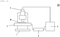
- FIG. 6 illustrates an example of the automatic inspecting apparatus.
- This automatic inspecting apparatus 10 comprises a microscope 1, an electrically-driven XY stage 2 on which an evaluation (observation) target wafer W is mounted and electrically movable in an XY direction, and an imaging camera 3 such as a digital camera.
- the automatic inspecting apparatus also comprises a controller 4 to control the apparatus.
- the automatic inspecting apparatus comprising a personal computer (PC) 5. Equipped with the PC 5, an operator can input measurement conditions and display measurement results on the PC monitor to check and analyze evaluation results.
- PC personal computer
- FIG. 1 shows a flowchart of the method for evaluating crystal defects in a silicon carbide single crystal wafer according to the present invention.
- a measurement target silicon carbide (SiC) single crystal wafer is etched with melted KOH to reveal crystal defects such as dislocation present in the silicon carbide single crystal wafer as a pit.
- An amount (condition) of the etching in this time is regulated so that a size of the etch pit due to a threading edge dislocation is 10 to 50 ⁇ m.
- Such a melted KOH etching condition can be adjusted by a temperature of the melted KOH, an etching time, etc., and the etching condition is determined in advance prior to the actual crystal evaluation.
- the size (10 to 50 ⁇ m) of the pit due to a threading edge dislocation is adopted as an index in order to precisely grasp and determine the presence of the etch pit when a microscopic image of a surface of the silicon carbide single crystal wafer is automatically photographed in the next step. That is, there are a larger amount of threading edge dislocations than other dislocations and the etch pit has a circular shape, and thereby the threading edge dislocation is most suitable as an index for setting the etching condition.
- the size of the etch pit due to the threading edge dislocation is smaller than 10 ⁇ m, the shape of the etch pit is unclear and may fail to be distinguished from a dust.
- the excessively large pit makes it difficult to precisely evaluate the dense state.
- microscopic images are obtained by automatic photographing at a plurality of positions on a surface of the silicon carbide single crystal wafer.
- an entire wafer can be photographed with a predetermined interval by controlling the electrically driven XY stage.
- the microscopic images are preferably automatically photographed with 2-mm interval so that an observation field size is 1 mm square.
- presence or absence of a defect dense part is determined in each of all the obtained microscopic images based on a continued length of the etch pit formed by the etching.
- the obtained microscopic images are image-analyzed, and a continued etch pit having a length equal to or longer than a predetermined length is judged as the defect dense part, for example.
- a microscopic image (picture) including such a defect dense part is judged as the presence of the defect dense part.
- FIG. 2 shows a microscopic image (observation field: 1.42 ⁇ 1.06 mm) showing a continued etch pit. A microscopic image in which the continued etch pit is observed as FIG. 2 is judged to have the defect dense part.
- FIG. 3 shows a microscopic image (observation field: 1.42 ⁇ 1.06 mm) without a continued etch pit. A microscopic image as FIG. 3 is judged not to have the defect dense part.
- the microscopic images are preferably judged to have the defect dense part when an etch pit having a continued length of 500 ⁇ m or longer is observed. This is because the presence or absence of the defect dense part can be more stably and more highly precisely determined by setting the continued length of the etch pit within such a range as a reference.
- the crystal defect of the evaluation target can be a micropipe, a threading helical dislocation, a threading edge dislocation, and a basal plane dislocation.
- the method for evaluating crystal defects according to the present invention is particularly suitable for evaluating the dense state of such crystal defects.
- the dense state in the silicon carbide single crystal wafer can be quantitatively evaluated.
- a ratio of a number of the microscopic images having the defect dense part (number of images having the defect dense part) to a total number of the obtained microscopic images (total number of the images) is preferably calculated and digitalized. This enables to compare wafers.
- the silicon carbide single crystal wafer can also be evaluated. This evaluation may be, for example, acceptance determination, and a condition of growing the single crystal can be reconsidered.
- an in-plane distribution of the crystal defects in the silicon carbide single crystal wafer can be evaluated.
- the in-plane distribution of the crystal defects can be visually evaluated by performing mapping from the positional information of the microscopic images to display the mapping on a monitor of the PC.
- the method for evaluating a silicon carbide single crystal wafer according to the present invention can observe many points in the wafer surface compared with a conventional manual observation, and enables to combine the mapping measurement and image analysis on the entire surface, which can easily grasp positions of the defect dense parts.
- a degree of the defect dense part can be digitalized and quantitatively evaluated.
- the silicon carbide single crystal wafer can be provided with a good degree of the defect dense part.
- the silicon carbide single crystal wafer with which a device can be manufactured with a good yield can be provided.
- Evaluation targets were silicon carbide single crystal wafers with 100 mm or 96 mm in diameter. These silicon carbide single crystal wafers were subjected to a selective etching treatment by using melted KOH melted at 500°C to reveal crystal defects (dislocation) as an etch pit so that a pit size due to a threading edge dislocation was approximately 30 ⁇ m. An entirety of this wafer was automatically photographed with 2-mm interval so that an observation size was 1 mm square by using the automatic inspecting apparatus illustrated in FIG. 6 with the imaging camera to control the electrically driven XY stage.
- Example of the present invention was able to easily evaluate the dense state of the defects regardless of operation skill of an operator.
Landscapes
- Chemical & Material Sciences (AREA)
- Engineering & Computer Science (AREA)
- Life Sciences & Earth Sciences (AREA)
- Health & Medical Sciences (AREA)
- Analytical Chemistry (AREA)
- Biochemistry (AREA)
- General Health & Medical Sciences (AREA)
- General Physics & Mathematics (AREA)
- Immunology (AREA)
- Pathology (AREA)
- Physics & Mathematics (AREA)
- Materials Engineering (AREA)
- Crystallography & Structural Chemistry (AREA)
- Metallurgy (AREA)
- Organic Chemistry (AREA)
- Inorganic Chemistry (AREA)
- Computer Vision & Pattern Recognition (AREA)
- Signal Processing (AREA)
- Testing Or Measuring Of Semiconductors Or The Like (AREA)
- Investigating Materials By The Use Of Optical Means Adapted For Particular Applications (AREA)
- Crystals, And After-Treatments Of Crystals (AREA)
- Chemical Kinetics & Catalysis (AREA)
- General Chemical & Material Sciences (AREA)
Abstract
Description
- The present invention relates to a method for evaluating crystal defects in a silicon carbide single crystal wafer.
- A power device using a silicon carbide (SiC) single crystal wafer has attracted attention in recent years since having features such as high breakdown voltage resistance, low loss, and operability at high temperature.
- The silicon carbide (SiC) single crystal wafer contains various crystal defects. Specifically, a micropipe, a threading helical dislocation, a threading edge dislocation, and a basal plane dislocation considerably adversely affect characteristics of electronic devices, and thereby precise evaluation therefor is extremely important for evaluation of substrate performance. In particular, required is a method for easily and simply detecting crystal defect density with high precision in a process for manufacturing a semiconductor substrate. A method for detecting crystal defects in a silicon carbide single crystal is proposed in, for example,
Patent Document 1. The method for evaluating dislocation density in the silicon carbide single crystal wafer described inPatent Document 1 evaluates performance by observing the wafer with a microscope. The crystal defects (dislocation) in the wafer are revealed as an etch pit by selective etching using melted alkali. - Patent Document 1:
JP 2011-151317 A - However, it is difficult to observe an entire surface of the wafer with the conventional microscope observation, and the observation is limited to local observation. Although a dislocation dense part causes a considerably large adverse effect, it is difficult to quantitatively evaluate a position and distribution of the dislocation dense part in the wafer surface and a degree of the dense part by the conventional local observation.
- The present invention has been made to solve the above problem. An object of the present invention is to provide a method for evaluating crystal defects in a silicon carbide single crystal wafer that can easily and simply evaluate the defect dense part of crystal defects, such as micropipes, threading helical dislocations, threading edge dislocations, and basal plane dislocations, in the silicon carbide single crystal wafer surface, specifically that can evaluate a position and distribution of the defect dense part and that can quantitatively evaluate a degree of the defect dense part.
- The present invention has been made to achieve the above object, and provides a method for evaluating crystal defects in a silicon carbide single crystal wafer, the method comprising steps of: etching a silicon carbide single crystal wafer with melted KOH so that a size of an etch pit due to a threading edge dislocation is 10 to 50 µm; obtaining microscopic images by automatic photographing at a plurality of positions on a surface of the silicon carbide single crystal wafer after the etching; determining presence or absence of a defect dense part in each of all the obtained microscopic images based on a continued length of the etch pit formed by the etching; and classifying all the obtained microscopic images into microscopic images having the defect dense part and microscopic images not having the defect dense part to evaluate a dense state of crystal defects in the silicon carbide single crystal wafer.
- Such a method for evaluating crystal defects in a silicon carbide single crystal wafer can easily and simply evaluate a dense state of the crystal defects in the silicon carbide single crystal wafer with high precision by revealing the crystal defects as the etch pit. By further inspecting the defect dense part by using this evaluation results and performing improvement or selection, a good silicon carbide single crystal wafer with reduced dense crystal defects can be provided. As a result, a silicon carbide single crystal wafer with which a device can be manufactured with a high yield can be provided.
- In this case, the method can be the method for evaluating crystal defects in a silicon carbide single crystal wafer wherein the microscopic images are judged to have the defect dense part when an etch pit having a continued length of 500 µm or longer is observed.
- This method can evaluate the crystal defects in the silicon carbide single crystal wafer more stably and certainly with high precision.
- In this case, the method can be the method for evaluating crystal defects in a silicon carbide single crystal wafer wherein the dense state of the crystal defects in the silicon carbide single crystal wafer is evaluated based on a ratio of a number of the microscopic images having the defect dense part to a total number of the obtained microscopic images.
- This method enables to easily and quantitatively evaluate a degree of the defect dense part on the silicon carbide single crystal wafer surface with digitalization.
- In this case, the method can be the method for evaluating crystal defects in a silicon carbide single crystal wafer wherein an in-plane distribution of the crystal defects in the silicon carbide single crystal wafer is evaluated based on positional information of the microscopic images having the defect dense part and positional information of the microscopic images not having the defect dense part.
- This method can grasp the position of the defect dense part on the silicon carbide single crystal wafer surface, and enables to easily evaluate the in-plane distribution.
- In this case, the method for evaluating crystal defects in a silicon carbide single crystal wafer can be a method in which the crystal defects are micropipes, threading helical dislocations, threading edge dislocations, and basal plane dislocations.
- The method for evaluating crystal defects according to the present invention is suitable for evaluating such crystal defects.
- In this case, the method can be the method for evaluating crystal defects in a silicon carbide single crystal wafer wherein the microscopic images are obtained by the automatic photographing by using an automatic inspecting apparatus having at least an electrically-driven XY stage, a microscope, and an imaging camera, and the obtained microscopic images are subjected to image analysis to judge presence or absence of the defect dense part.
- This method can stably and easily evaluate the crystal defects in a short time regardless of difference in the skill and proficiency of the measurers, etc.
- As noted above, the inventive method for evaluating crystal defects in the silicon carbide single crystal wafer can easily and simply evaluate the dense state of the crystal defects in the silicon carbide single crystal wafer with high precision by revealing the crystal defects as the etch pit. By further inspecting the defect dense part by using this evaluation result and performing improvement or selection, a good silicon carbide single crystal wafer with reduced dense crystal defects can be provided. As a result, the silicon carbide single crystal wafer that can manufacture a device with a good yield can be provided.
-
-
FIG. 1 shows a schematic flowchart of the method for evaluating crystal defects in a silicon carbide single crystal wafer according to the present invention. -
FIG. 2 shows a microscopic image showing a continued etch pit. -
FIG. 3 shows a microscopic image without a continued etch pit. -
FIG. 4 shows a mapping of microscopic images in which presence or absence of a defect dense part is classified in Example (wafer with 100 mm in diameter). -
FIG. 5 shows a mapping of microscopic images in which presence or absence of a defect dense part is classified in Example (wafer with 96 mm in diameter). -
FIG. 6 illustrates an automatic inspecting apparatus suitably used for the method for evaluating crystal defects in a silicon carbide single crystal wafer according to the present invention. - Hereinafter, the present invention will be described in detail, but the present invention is not limited thereto.
- As noted above, required is a method that can evaluate the position and distribution of a dense part of crystal defects in the silicon carbide single crystal wafer surface, such as a micropipe, a threading helical dislocation, a threading edge dislocation, and a basal plane dislocation, and that can quantitatively evaluate a degree of the dense part.
- The present inventors have made earnest study on the above problem, and consequently have found that the dense state of the crystal defects in the silicon carbide single crystal wafer can be easily and simply evaluated with high precision by a method for evaluating crystal defects in a silicon carbide single crystal wafer, the method comprising steps of: etching a silicon carbide single crystal wafer with melted KOH so that a size of an etch pit due to a threading edge dislocation is 10 to 50 µm; obtaining microscopic images by automatic photographing at a plurality of positions on a surface of the silicon carbide single crystal wafer after the etching; determining presence or absence of a defect dense part in each of all the obtained microscopic images based on a continued length of the etch pit formed by the etching; and classifying all the obtained microscopic images into microscopic images having the defect dense part and microscopic images not having the defect dense part to evaluate a dense state of crystal defects in the silicon carbide single crystal wafer. This finding has led to complete the present invention.
- Hereinafter, the description will be made with reference to the drawings.
- First, an automatic inspecting apparatus suitably used for the method for evaluating crystal defects in the silicon carbide single crystal wafer according to the present invention will be described.
FIG. 6 illustrates an example of the automatic inspecting apparatus. Thisautomatic inspecting apparatus 10 comprises amicroscope 1, an electrically-drivenXY stage 2 on which an evaluation (observation) target wafer W is mounted and electrically movable in an XY direction, and animaging camera 3 such as a digital camera. The automatic inspecting apparatus also comprises acontroller 4 to control the apparatus. Furthermore, the automatic inspecting apparatus comprising a personal computer (PC) 5. Equipped with thePC 5, an operator can input measurement conditions and display measurement results on the PC monitor to check and analyze evaluation results. - Next, the method for evaluating crystal defects in a silicon carbide single crystal wafer according to the present invention will be described.
FIG. 1 shows a flowchart of the method for evaluating crystal defects in a silicon carbide single crystal wafer according to the present invention. - First, as shown in
FIG. 1(a) , a measurement target silicon carbide (SiC) single crystal wafer is etched with melted KOH to reveal crystal defects such as dislocation present in the silicon carbide single crystal wafer as a pit. An amount (condition) of the etching in this time is regulated so that a size of the etch pit due to a threading edge dislocation is 10 to 50 µm. Such a melted KOH etching condition can be adjusted by a temperature of the melted KOH, an etching time, etc., and the etching condition is determined in advance prior to the actual crystal evaluation. - Here, the size (10 to 50 µm) of the pit due to a threading edge dislocation is adopted as an index in order to precisely grasp and determine the presence of the etch pit when a microscopic image of a surface of the silicon carbide single crystal wafer is automatically photographed in the next step. That is, there are a larger amount of threading edge dislocations than other dislocations and the etch pit has a circular shape, and thereby the threading edge dislocation is most suitable as an index for setting the etching condition. With etching so that the size of the etch pit due to the threading edge dislocation is smaller than 10 µm, the shape of the etch pit is unclear and may fail to be distinguished from a dust. Meanwhile, with etching so that the size of the etch pit due to the threading edge dislocation is larger than 50 µm, the excessively large pit makes it difficult to precisely evaluate the dense state.
- Then, as shown in
FIG. 1(b) , microscopic images are obtained by automatic photographing at a plurality of positions on a surface of the silicon carbide single crystal wafer. By using the automatic inspecting apparatus described as above, an entire wafer can be photographed with a predetermined interval by controlling the electrically driven XY stage. For example, the microscopic images are preferably automatically photographed with 2-mm interval so that an observation field size is 1 mm square. - Then, presence or absence of a defect dense part is determined in each of all the obtained microscopic images based on a continued length of the etch pit formed by the etching. As shown in
FIG. 1(c) , the obtained microscopic images are image-analyzed, and a continued etch pit having a length equal to or longer than a predetermined length is judged as the defect dense part, for example. A microscopic image (picture) including such a defect dense part is judged as the presence of the defect dense part. -
FIG. 2 shows a microscopic image (observation field: 1.42×1.06 mm) showing a continued etch pit. A microscopic image in which the continued etch pit is observed asFIG. 2 is judged to have the defect dense part.FIG. 3 shows a microscopic image (observation field: 1.42×1.06 mm) without a continued etch pit. A microscopic image asFIG. 3 is judged not to have the defect dense part. - In this time, the microscopic images are preferably judged to have the defect dense part when an etch pit having a continued length of 500 µm or longer is observed. This is because the presence or absence of the defect dense part can be more stably and more highly precisely determined by setting the continued length of the etch pit within such a range as a reference.
- The crystal defect of the evaluation target can be a micropipe, a threading helical dislocation, a threading edge dislocation, and a basal plane dislocation. The method for evaluating crystal defects according to the present invention is particularly suitable for evaluating the dense state of such crystal defects.
- As shown in
FIG. 1(d) , all the obtained microscopic images are classified into microscopic images having the defect dense part and microscopic images not having the defect dense part. Then, the dense state of the crystal defects in the silicon carbide single crystal wafer is evaluated by using this classification results. - Next, a specific example of the evaluation of the dense state of the crystal defects will be described. For example, the dense state in the silicon carbide single crystal wafer can be quantitatively evaluated. In this case, a ratio of a number of the microscopic images having the defect dense part (number of images having the defect dense part) to a total number of the obtained microscopic images (total number of the images) is preferably calculated and digitalized. This enables to compare wafers. Based on the digitalized value, the silicon carbide single crystal wafer can also be evaluated. This evaluation may be, for example, acceptance determination, and a condition of growing the single crystal can be reconsidered.
- Based on positional information of the microscopic images having the defect dense part and positional information of the microscopic images not having the defect dense part, an in-plane distribution of the crystal defects in the silicon carbide single crystal wafer can be evaluated. In this case, the in-plane distribution of the crystal defects can be visually evaluated by performing mapping from the positional information of the microscopic images to display the mapping on a monitor of the PC.
- As described above in detail, the method for evaluating a silicon carbide single crystal wafer according to the present invention can observe many points in the wafer surface compared with a conventional manual observation, and enables to combine the mapping measurement and image analysis on the entire surface, which can easily grasp positions of the defect dense parts. In addition, a degree of the defect dense part can be digitalized and quantitatively evaluated. By further inspecting the defect dense part base on such results to improve the wafer manufacturing condition or by selecting the manufactured wafers, the silicon carbide single crystal wafer can be provided with a good degree of the defect dense part. As a result, the silicon carbide single crystal wafer with which a device can be manufactured with a good yield can be provided.
- Hereinafter, the present invention will be specifically described with Example, but this Example does not limit the present invention.
- Evaluation targets were silicon carbide single crystal wafers with 100 mm or 96 mm in diameter. These silicon carbide single crystal wafers were subjected to a selective etching treatment by using melted KOH melted at 500°C to reveal crystal defects (dislocation) as an etch pit so that a pit size due to a threading edge dislocation was approximately 30 µm. An entirety of this wafer was automatically photographed with 2-mm interval so that an observation size was 1 mm square by using the automatic inspecting apparatus illustrated in
FIG. 6 with the imaging camera to control the electrically driven XY stage. In the wafer with 100 mm in diameter, 1789 microscopic images were automatically photographed, presence or absence of a defect dense part was determined when the etch pit had a continued length of 800 µm or longer was judged to have the defect dense part, and the microscopic images were classified. Mapping the microscopic images classified as above based on positional information yielded a map asFIG. 4 . InFIG. 4 , a cell indicated in black is the image having the defect dense part. As shown inFIG. 4 , 73 images were judged to have the defect dense part, and a ratio of the images having the defect dense part was 73/1789 = 4.1%. On the wafer with 96 mm in diameter, 1741 microscopic images were automatically photographed by the similar method, and the etch pit having a continued length of 800 µm or longer was judged to have the defect dense part, resulting in a map asFIG. 5 . As shown inFIG. 5 , 23 images were judged to have the defect dense part, and a ratio of the images having the defect dense part was 23/1741 = 1.3%. The mapping as above enabled to visualize the distribution of the defect dense part for easy grasp. The digitalization enabled to quantitatively the dense state of the defects. - With the same wafer as in Example that was subjected to the selective etching with melted KOH, the wafer surface was visually observed with a microscope manually. The presence of the defect dense part was able to be confirmed, but it was difficult to precisely grasp the positions of the defect dense part and to perform quantitative evaluation with digitalization. The difference in the dense states of the defects between the two wafers was not obviously determined.
- As above, Example of the present invention was able to easily evaluate the dense state of the defects regardless of operation skill of an operator.
- It should be noted that the present invention is not limited to the above-described embodiments. The embodiments are just examples, and any examples that substantially have the same feature and demonstrate the same functions and effects as those in the technical concept disclosed in claims of the present invention are included in the technical scope of the present invention.
Claims (6)
- A method for evaluating crystal defects in a silicon carbide single crystal wafer, the method comprising steps of:etching a silicon carbide single crystal wafer with melted KOH so that a size of an etch pit due to a threading edge dislocation is 10 to 50 µm;obtaining microscopic images by automatic photographing at a plurality of positions on a surface of the silicon carbide single crystal wafer after the etching;determining presence or absence of a defect dense part in each of all the obtained microscopic images based on a continued length of the etch pit formed by the etching; andclassifying all the obtained microscopic images into microscopic images having the defect dense part and microscopic images not having the defect dense part to evaluate a dense state of crystal defects in the silicon carbide single crystal wafer.
- The method for evaluating crystal defects in a silicon carbide single crystal wafer according to claim 1, wherein the microscopic images are judged to have the defect dense part when an etch pit having a continued length of 500 µm or longer is observed.
- The method for evaluating crystal defects in a silicon carbide single crystal wafer according to claim 1 or 2, wherein the dense state of the crystal defects in the silicon carbide single crystal wafer is evaluated based on a ratio of a number of the microscopic images having the defect dense part to a total number of the obtained microscopic images.
- The method for evaluating crystal defects in a silicon carbide single crystal wafer according to any one of claims 1 to 3, wherein an in-plane distribution of the crystal defects in the silicon carbide single crystal wafer is evaluated based on positional information of the microscopic images having the defect dense part and positional information of the microscopic images not having the defect dense part.
- The method for evaluating crystal defects in a silicon carbide single crystal wafer according to any one of claims 1 to 4, wherein the crystal defects are micropipes, threading helical dislocations, threading edge dislocations, and basal plane dislocations.
- The method for evaluating crystal defects in a silicon carbide single crystal wafer according to any one of claims 1 to 5, wherein the microscopic images are obtained by the automatic photographing by using an automatic inspecting apparatus having at least an electrically-driven XY stage, a microscope, and an imaging camera, and the obtained microscopic images are subjected to image analysis to judge presence or absence of the defect dense part.
Applications Claiming Priority (2)
| Application Number | Priority Date | Filing Date | Title |
|---|---|---|---|
| JP2021042104A JP7494768B2 (en) | 2021-03-16 | 2021-03-16 | Method for evaluating crystal defects in silicon carbide single crystal wafers |
| PCT/JP2022/007910 WO2022196292A1 (en) | 2021-03-16 | 2022-02-25 | Method for evaluating crystal defects of silicon carbide single crystal wafer |
Publications (2)
| Publication Number | Publication Date |
|---|---|
| EP4310893A1 true EP4310893A1 (en) | 2024-01-24 |
| EP4310893A4 EP4310893A4 (en) | 2025-03-19 |
Family
ID=83321263
Family Applications (1)
| Application Number | Title | Priority Date | Filing Date |
|---|---|---|---|
| EP22771048.0A Pending EP4310893A4 (en) | 2021-03-16 | 2022-02-25 | Method for evaluating crystal defects in a silicon carbide single-crystal wafer |
Country Status (7)
| Country | Link |
|---|---|
| US (1) | US12345660B2 (en) |
| EP (1) | EP4310893A4 (en) |
| JP (1) | JP7494768B2 (en) |
| KR (1) | KR20230156348A (en) |
| CN (1) | CN116918052A (en) |
| TW (1) | TWI914506B (en) |
| WO (1) | WO2022196292A1 (en) |
Families Citing this family (2)
| Publication number | Priority date | Publication date | Assignee | Title |
|---|---|---|---|---|
| JP7494768B2 (en) * | 2021-03-16 | 2024-06-04 | 信越半導体株式会社 | Method for evaluating crystal defects in silicon carbide single crystal wafers |
| TWI890143B (en) * | 2023-09-20 | 2025-07-11 | 環球晶圓股份有限公司 | Method of identifying defects in crystals |
Family Cites Families (33)
| Publication number | Priority date | Publication date | Assignee | Title |
|---|---|---|---|---|
| JPH0622191B2 (en) * | 1983-09-07 | 1994-03-23 | 日本電信電話株式会社 | Compound semiconductor crystal substrate for FET fabrication |
| US5958132A (en) * | 1991-04-18 | 1999-09-28 | Nippon Steel Corporation | SiC single crystal and method for growth thereof |
| US7018554B2 (en) * | 2003-09-22 | 2006-03-28 | Cree, Inc. | Method to reduce stacking fault nucleation sites and reduce forward voltage drift in bipolar devices |
| US7173285B2 (en) * | 2004-03-18 | 2007-02-06 | Cree, Inc. | Lithographic methods to reduce stacking fault nucleation sites |
| JP4850663B2 (en) * | 2006-11-02 | 2012-01-11 | 新日本製鐵株式会社 | Method for producing SiC single crystal and method for producing SiC single crystal substrate |
| CN101802273B (en) * | 2007-09-12 | 2013-04-17 | 昭和电工株式会社 | Epitaxial SIC single crystal substrate and method for manufacturing epitaxial SIC single crystal substrate |
| JP2010095397A (en) * | 2008-10-15 | 2010-04-30 | Nippon Steel Corp | Silicon carbide single crystal and silicon carbide single crystal wafer |
| JP4758492B2 (en) * | 2009-03-24 | 2011-08-31 | トヨタ自動車株式会社 | Single crystal defect density measurement method |
| JP5167208B2 (en) * | 2009-07-21 | 2013-03-21 | トヨタ自動車株式会社 | Method and apparatus for measuring defect density of single crystal |
| JP5519305B2 (en) | 2010-01-25 | 2014-06-11 | トヨタ自動車株式会社 | Method for detecting defects in silicon carbide single crystal |
| JP4850960B2 (en) * | 2010-04-07 | 2012-01-11 | 新日本製鐵株式会社 | Epitaxial silicon carbide single crystal substrate manufacturing method |
| KR101530057B1 (en) * | 2011-08-29 | 2015-06-18 | 신닛테츠스미킨 카부시키카이샤 | Silicon carbide single crystal wafer and manufacturing method for same |
| JP5961357B2 (en) * | 2011-09-09 | 2016-08-02 | 昭和電工株式会社 | SiC epitaxial wafer and manufacturing method thereof |
| US8900979B2 (en) * | 2011-11-23 | 2014-12-02 | University Of South Carolina | Pretreatment method for reduction and/or elimination of basal plane dislocations close to epilayer/substrate interface in growth of SiC epitaxial films |
| US9797064B2 (en) * | 2013-02-05 | 2017-10-24 | Dow Corning Corporation | Method for growing a SiC crystal by vapor deposition onto a seed crystal provided on a support shelf which permits thermal expansion |
| US9738991B2 (en) * | 2013-02-05 | 2017-08-22 | Dow Corning Corporation | Method for growing a SiC crystal by vapor deposition onto a seed crystal provided on a supporting shelf which permits thermal expansion |
| JP6052934B2 (en) * | 2013-08-14 | 2016-12-27 | 株式会社日立製作所 | Semiconductor inspection method, semiconductor inspection apparatus, and semiconductor element manufacturing method |
| JP6197722B2 (en) * | 2014-03-26 | 2017-09-20 | 新日鐵住金株式会社 | Method for evaluating in-plane distribution of dislocations in SiC plate |
| CN105658846B (en) * | 2014-09-30 | 2018-08-28 | 昭和电工株式会社 | The manufacturing method of silicon carbide single crystal wafer and single-crystal silicon carbide ingot |
| US10030319B2 (en) | 2014-11-27 | 2018-07-24 | Sumitomo Electric Industries, Ltd. | Silicon carbide substrate, method for producing same, and method for manufacturing silicon carbide semiconductor device |
| JP6524233B2 (en) * | 2015-07-29 | 2019-06-05 | 昭和電工株式会社 | Method of manufacturing epitaxial silicon carbide single crystal wafer |
| JP6690282B2 (en) * | 2016-02-15 | 2020-04-28 | 住友電気工業株式会社 | Silicon carbide epitaxial substrate and method for manufacturing silicon carbide semiconductor device |
| JP2018131350A (en) * | 2017-02-14 | 2018-08-23 | 株式会社豊田自動織機 | Semiconductor substrate |
| WO2018160785A1 (en) * | 2017-03-02 | 2018-09-07 | University Of South Carolina | PINNING THE CONVERSION POINT BELOW THE EPILAYER INTERFACE FOR SiC POWER DEVICE |
| DE112018000035T5 (en) * | 2017-03-30 | 2019-02-28 | Showa Denko K.K. | A method of quality evaluation of a SiC single crystal body and a method of producing a silicon carbide single crystal ingot using the same |
| JP6784220B2 (en) * | 2017-04-14 | 2020-11-11 | 信越化学工業株式会社 | Method for manufacturing SiC single crystal |
| JP7085833B2 (en) * | 2017-12-25 | 2022-06-17 | 昭和電工株式会社 | Method for manufacturing silicon carbide single crystal |
| WO2021025084A1 (en) * | 2019-08-06 | 2021-02-11 | 学校法人関西学院 | SiC SEED CRYSTAL AND METHOD FOR PRODUCING SAME, SiC INGOT PRODUCED BY GROWING SAID SiC SEED CRYSTAL AND METHOD FOR PRODUCING SAME, AND SiC WAFER PRODUCED FROM SAID SiC INGOT AND SiC WAFER WITH EPITAXIAL FILM AND METHODS RESPECTIVELY FOR PRODUCING SAID SiC WAFER AND SAID SiC WAFER WITH EPITAXIAL FILM |
| EP4012077A4 (en) * | 2019-08-06 | 2023-09-20 | Kwansei Gakuin Educational Foundation | METHOD FOR PRODUCING SIC SUBSTRATE |
| JP7393900B2 (en) * | 2019-09-24 | 2023-12-07 | 一般財団法人電力中央研究所 | Method for manufacturing silicon carbide single crystal wafer and silicon carbide single crystal ingot |
| CN114423889B (en) * | 2019-09-27 | 2024-07-09 | 学校法人关西学院 | Method for producing SiC single crystal, device for producing SiC single crystal, and SiC single crystal wafer |
| WO2022190458A1 (en) * | 2021-03-12 | 2022-09-15 | 住友電気工業株式会社 | Silicon carbide substrate and silicon carbide substrate manufacturing method |
| JP7494768B2 (en) * | 2021-03-16 | 2024-06-04 | 信越半導体株式会社 | Method for evaluating crystal defects in silicon carbide single crystal wafers |
-
2021
- 2021-03-16 JP JP2021042104A patent/JP7494768B2/en active Active
-
2022
- 2022-02-25 KR KR1020237031063A patent/KR20230156348A/en active Pending
- 2022-02-25 EP EP22771048.0A patent/EP4310893A4/en active Pending
- 2022-02-25 WO PCT/JP2022/007910 patent/WO2022196292A1/en not_active Ceased
- 2022-02-25 CN CN202280019273.3A patent/CN116918052A/en active Pending
- 2022-02-25 US US18/280,825 patent/US12345660B2/en active Active
- 2022-03-07 TW TW111108114A patent/TWI914506B/en active
Also Published As
| Publication number | Publication date |
|---|---|
| JP7494768B2 (en) | 2024-06-04 |
| US20240142390A1 (en) | 2024-05-02 |
| JP2022142095A (en) | 2022-09-30 |
| WO2022196292A1 (en) | 2022-09-22 |
| CN116918052A (en) | 2023-10-20 |
| US12345660B2 (en) | 2025-07-01 |
| TW202300903A (en) | 2023-01-01 |
| TWI914506B (en) | 2026-02-11 |
| KR20230156348A (en) | 2023-11-14 |
| EP4310893A4 (en) | 2025-03-19 |
Similar Documents
| Publication | Publication Date | Title |
|---|---|---|
| US5777327A (en) | Pattern shape inspection apparatus for forming specimen image on display apparatus | |
| US12345660B2 (en) | Method for evaluating crystal defects in silicon carbide single crystal wafer | |
| US9335277B2 (en) | Region-of-interest determination apparatus, observation tool or inspection tool, region-of-interest determination method, and observation method or inspection method using region-of-interest determination method | |
| JP3993817B2 (en) | Defect composition analysis method and apparatus | |
| US20090268959A1 (en) | Method and apparatus for reviewing defects | |
| US8664596B2 (en) | Method for characterizing identified defects during charged particle beam inspection and application thereof | |
| US20130108147A1 (en) | Inspection method and device therefor | |
| TW200944784A (en) | Inspection detecting method | |
| JP2016156812A (en) | Pattern matching using slices of known shape for automated S / TEM acquisition and measurement | |
| TW202305321A (en) | Crystal defect detection method and detection device | |
| JP2001127129A (en) | Sample defect inspection system and inspection method | |
| US12228523B2 (en) | Method of evaluating SiC substrate, method of manufacturing SiC epitaxial wafer, and method of manufacturing SiC device | |
| KR100963131B1 (en) | How to automatically inspect wafer defects | |
| US20180219069A1 (en) | Silicon carbide single crystal, silicon carbide single crystal wafer, silicon carbide single crystal epitaxial wafer, and electronic device | |
| CN108508053B (en) | Method for detecting systematic infinitesimal physical defects | |
| JP5604196B2 (en) | Macro inspection method and inspection system | |
| US20070024963A1 (en) | Method of observing defect and observation apparatus using microscope | |
| EP4497855A1 (en) | Method for evaluating sic substrate, method for manufacturing sic substrate, and sic substrate evaluation device | |
| KR20090048524A (en) | Indentation test method of LCD panel inspection system | |
| CN111883450B (en) | Method for improving yield of gallium nitride device | |
| JP2013118333A (en) | Method for evaluating defect of epitaxial wafer | |
| JP2026078891A (en) | Crystal evaluation methods, crystal evaluation equipment, SiC substrates, SiC devices, SiC epitaxial wafers | |
| US11557457B2 (en) | Charged particle beam apparatus | |
| US20260118295A1 (en) | CRYSTAL EVALUATION METHOD, CRYSTAL EVALUATION DEVICE, SiC SUBSTRATE, SiC DEVICE, AND SiC EPITAXIAL WAFER | |
| Larsen et al. | Automatic determination of recrystallization parameters in metals by electron backscatter pattern line scans |
Legal Events
| Date | Code | Title | Description |
|---|---|---|---|
| STAA | Information on the status of an ep patent application or granted ep patent |
Free format text: STATUS: THE INTERNATIONAL PUBLICATION HAS BEEN MADE |
|
| PUAI | Public reference made under article 153(3) epc to a published international application that has entered the european phase |
Free format text: ORIGINAL CODE: 0009012 |
|
| STAA | Information on the status of an ep patent application or granted ep patent |
Free format text: STATUS: REQUEST FOR EXAMINATION WAS MADE |
|
| 17P | Request for examination filed |
Effective date: 20230907 |
|
| AK | Designated contracting states |
Kind code of ref document: A1 Designated state(s): AL AT BE BG CH CY CZ DE DK EE ES FI FR GB GR HR HU IE IS IT LI LT LU LV MC MK MT NL NO PL PT RO RS SE SI SK SM TR |
|
| DAV | Request for validation of the european patent (deleted) | ||
| DAX | Request for extension of the european patent (deleted) | ||
| A4 | Supplementary search report drawn up and despatched |
Effective date: 20250219 |
|
| RIC1 | Information provided on ipc code assigned before grant |
Ipc: G01N 21/95 20060101ALI20250213BHEP Ipc: G01N 21/956 20060101ALI20250213BHEP Ipc: C30B 29/36 20060101ALI20250213BHEP Ipc: H01L 21/66 20060101AFI20250213BHEP |