EP4303941A1 - Light-emitting device and method for manufacturing light-emitting device - Google Patents
Light-emitting device and method for manufacturing light-emitting device Download PDFInfo
- Publication number
- EP4303941A1 EP4303941A1 EP22763032.4A EP22763032A EP4303941A1 EP 4303941 A1 EP4303941 A1 EP 4303941A1 EP 22763032 A EP22763032 A EP 22763032A EP 4303941 A1 EP4303941 A1 EP 4303941A1
- Authority
- EP
- European Patent Office
- Prior art keywords
- light emitting
- film
- light
- compound semiconductor
- semiconductor layer
- Prior art date
- Legal status (The legal status is an assumption and is not a legal conclusion. Google has not performed a legal analysis and makes no representation as to the accuracy of the status listed.)
- Pending
Links
Images











Classifications
-
- G—PHYSICS
- G09—EDUCATION; CRYPTOGRAPHY; DISPLAY; ADVERTISING; SEALS
- G09F—DISPLAYING; ADVERTISING; SIGNS; LABELS OR NAME-PLATES; SEALS
- G09F9/00—Indicating arrangements for variable information in which the information is built-up on a support by selection or combination of individual elements
- G09F9/30—Indicating arrangements for variable information in which the information is built-up on a support by selection or combination of individual elements in which the desired character or characters are formed by combining individual elements
- G09F9/33—Indicating arrangements for variable information in which the information is built-up on a support by selection or combination of individual elements in which the desired character or characters are formed by combining individual elements being semiconductor devices, e.g. diodes
-
- H—ELECTRICITY
- H10—SEMICONDUCTOR DEVICES; ELECTRIC SOLID-STATE DEVICES NOT OTHERWISE PROVIDED FOR
- H10D—INORGANIC ELECTRIC SEMICONDUCTOR DEVICES
- H10D86/00—Integrated devices formed in or on insulating or conducting substrates, e.g. formed in silicon-on-insulator [SOI] substrates or on stainless steel or glass substrates
- H10D86/40—Integrated devices formed in or on insulating or conducting substrates, e.g. formed in silicon-on-insulator [SOI] substrates or on stainless steel or glass substrates characterised by multiple TFTs
- H10D86/441—Interconnections, e.g. scanning lines
-
- H—ELECTRICITY
- H10—SEMICONDUCTOR DEVICES; ELECTRIC SOLID-STATE DEVICES NOT OTHERWISE PROVIDED FOR
- H10D—INORGANIC ELECTRIC SEMICONDUCTOR DEVICES
- H10D86/00—Integrated devices formed in or on insulating or conducting substrates, e.g. formed in silicon-on-insulator [SOI] substrates or on stainless steel or glass substrates
- H10D86/40—Integrated devices formed in or on insulating or conducting substrates, e.g. formed in silicon-on-insulator [SOI] substrates or on stainless steel or glass substrates characterised by multiple TFTs
- H10D86/60—Integrated devices formed in or on insulating or conducting substrates, e.g. formed in silicon-on-insulator [SOI] substrates or on stainless steel or glass substrates characterised by multiple TFTs wherein the TFTs are in active matrices
-
- H—ELECTRICITY
- H10—SEMICONDUCTOR DEVICES; ELECTRIC SOLID-STATE DEVICES NOT OTHERWISE PROVIDED FOR
- H10H—INORGANIC LIGHT-EMITTING SEMICONDUCTOR DEVICES HAVING POTENTIAL BARRIERS
- H10H20/00—Individual inorganic light-emitting semiconductor devices having potential barriers, e.g. light-emitting diodes [LED]
- H10H20/01—Manufacture or treatment
- H10H20/011—Manufacture or treatment of bodies, e.g. forming semiconductor layers
- H10H20/013—Manufacture or treatment of bodies, e.g. forming semiconductor layers having light-emitting regions comprising only Group III-V materials
- H10H20/0133—Manufacture or treatment of bodies, e.g. forming semiconductor layers having light-emitting regions comprising only Group III-V materials with a substrate not being Group III-V materials
- H10H20/01335—Manufacture or treatment of bodies, e.g. forming semiconductor layers having light-emitting regions comprising only Group III-V materials with a substrate not being Group III-V materials the light-emitting regions comprising nitride materials
-
- H—ELECTRICITY
- H10—SEMICONDUCTOR DEVICES; ELECTRIC SOLID-STATE DEVICES NOT OTHERWISE PROVIDED FOR
- H10H—INORGANIC LIGHT-EMITTING SEMICONDUCTOR DEVICES HAVING POTENTIAL BARRIERS
- H10H20/00—Individual inorganic light-emitting semiconductor devices having potential barriers, e.g. light-emitting diodes [LED]
- H10H20/01—Manufacture or treatment
- H10H20/011—Manufacture or treatment of bodies, e.g. forming semiconductor layers
- H10H20/018—Bonding of wafers
-
- H—ELECTRICITY
- H10—SEMICONDUCTOR DEVICES; ELECTRIC SOLID-STATE DEVICES NOT OTHERWISE PROVIDED FOR
- H10H—INORGANIC LIGHT-EMITTING SEMICONDUCTOR DEVICES HAVING POTENTIAL BARRIERS
- H10H20/00—Individual inorganic light-emitting semiconductor devices having potential barriers, e.g. light-emitting diodes [LED]
- H10H20/80—Constructional details
- H10H20/83—Electrodes
- H10H20/832—Electrodes characterised by their material
- H10H20/833—Transparent materials
-
- H—ELECTRICITY
- H10—SEMICONDUCTOR DEVICES; ELECTRIC SOLID-STATE DEVICES NOT OTHERWISE PROVIDED FOR
- H10H—INORGANIC LIGHT-EMITTING SEMICONDUCTOR DEVICES HAVING POTENTIAL BARRIERS
- H10H20/00—Individual inorganic light-emitting semiconductor devices having potential barriers, e.g. light-emitting diodes [LED]
- H10H20/80—Constructional details
- H10H20/84—Coatings, e.g. passivation layers or antireflective coatings
- H10H20/841—Reflective coatings, e.g. dielectric Bragg reflectors
-
- H—ELECTRICITY
- H10—SEMICONDUCTOR DEVICES; ELECTRIC SOLID-STATE DEVICES NOT OTHERWISE PROVIDED FOR
- H10H—INORGANIC LIGHT-EMITTING SEMICONDUCTOR DEVICES HAVING POTENTIAL BARRIERS
- H10H20/00—Individual inorganic light-emitting semiconductor devices having potential barriers, e.g. light-emitting diodes [LED]
- H10H20/80—Constructional details
- H10H20/85—Packages
- H10H20/851—Wavelength conversion means
-
- H—ELECTRICITY
- H10—SEMICONDUCTOR DEVICES; ELECTRIC SOLID-STATE DEVICES NOT OTHERWISE PROVIDED FOR
- H10H—INORGANIC LIGHT-EMITTING SEMICONDUCTOR DEVICES HAVING POTENTIAL BARRIERS
- H10H20/00—Individual inorganic light-emitting semiconductor devices having potential barriers, e.g. light-emitting diodes [LED]
- H10H20/80—Constructional details
- H10H20/85—Packages
- H10H20/855—Optical field-shaping means, e.g. lenses
-
- H—ELECTRICITY
- H10—SEMICONDUCTOR DEVICES; ELECTRIC SOLID-STATE DEVICES NOT OTHERWISE PROVIDED FOR
- H10H—INORGANIC LIGHT-EMITTING SEMICONDUCTOR DEVICES HAVING POTENTIAL BARRIERS
- H10H20/00—Individual inorganic light-emitting semiconductor devices having potential barriers, e.g. light-emitting diodes [LED]
- H10H20/80—Constructional details
- H10H20/85—Packages
- H10H20/857—Interconnections, e.g. lead-frames, bond wires or solder balls
-
- H—ELECTRICITY
- H10—SEMICONDUCTOR DEVICES; ELECTRIC SOLID-STATE DEVICES NOT OTHERWISE PROVIDED FOR
- H10H—INORGANIC LIGHT-EMITTING SEMICONDUCTOR DEVICES HAVING POTENTIAL BARRIERS
- H10H29/00—Integrated devices, or assemblies of multiple devices, comprising at least one light-emitting semiconductor element covered by group H10H20/00
- H10H29/10—Integrated devices comprising at least one light-emitting semiconductor component covered by group H10H20/00
- H10H29/14—Integrated devices comprising at least one light-emitting semiconductor component covered by group H10H20/00 comprising multiple light-emitting semiconductor components
- H10H29/142—Two-dimensional arrangements, e.g. asymmetric LED layout
-
- H—ELECTRICITY
- H10—SEMICONDUCTOR DEVICES; ELECTRIC SOLID-STATE DEVICES NOT OTHERWISE PROVIDED FOR
- H10P—GENERIC PROCESSES OR APPARATUS FOR THE MANUFACTURE OR TREATMENT OF DEVICES COVERED BY CLASS H10
- H10P54/00—Cutting or separating of wafers, substrates or parts of devices
-
- H—ELECTRICITY
- H10—SEMICONDUCTOR DEVICES; ELECTRIC SOLID-STATE DEVICES NOT OTHERWISE PROVIDED FOR
- H10W—GENERIC PACKAGES, INTERCONNECTIONS, CONNECTORS OR OTHER CONSTRUCTIONAL DETAILS OF DEVICES COVERED BY CLASS H10
- H10W90/00—Package configurations
-
- H—ELECTRICITY
- H10—SEMICONDUCTOR DEVICES; ELECTRIC SOLID-STATE DEVICES NOT OTHERWISE PROVIDED FOR
- H10H—INORGANIC LIGHT-EMITTING SEMICONDUCTOR DEVICES HAVING POTENTIAL BARRIERS
- H10H20/00—Individual inorganic light-emitting semiconductor devices having potential barriers, e.g. light-emitting diodes [LED]
- H10H20/01—Manufacture or treatment
- H10H20/032—Manufacture or treatment of electrodes
-
- H—ELECTRICITY
- H10—SEMICONDUCTOR DEVICES; ELECTRIC SOLID-STATE DEVICES NOT OTHERWISE PROVIDED FOR
- H10H—INORGANIC LIGHT-EMITTING SEMICONDUCTOR DEVICES HAVING POTENTIAL BARRIERS
- H10H20/00—Individual inorganic light-emitting semiconductor devices having potential barriers, e.g. light-emitting diodes [LED]
- H10H20/01—Manufacture or treatment
- H10H20/034—Manufacture or treatment of coatings
-
- H—ELECTRICITY
- H10—SEMICONDUCTOR DEVICES; ELECTRIC SOLID-STATE DEVICES NOT OTHERWISE PROVIDED FOR
- H10H—INORGANIC LIGHT-EMITTING SEMICONDUCTOR DEVICES HAVING POTENTIAL BARRIERS
- H10H20/00—Individual inorganic light-emitting semiconductor devices having potential barriers, e.g. light-emitting diodes [LED]
- H10H20/01—Manufacture or treatment
- H10H20/036—Manufacture or treatment of packages
- H10H20/0364—Manufacture or treatment of packages of interconnections
-
- H—ELECTRICITY
- H10—SEMICONDUCTOR DEVICES; ELECTRIC SOLID-STATE DEVICES NOT OTHERWISE PROVIDED FOR
- H10H—INORGANIC LIGHT-EMITTING SEMICONDUCTOR DEVICES HAVING POTENTIAL BARRIERS
- H10H20/00—Individual inorganic light-emitting semiconductor devices having potential barriers, e.g. light-emitting diodes [LED]
- H10H20/80—Constructional details
- H10H20/83—Electrodes
- H10H20/831—Electrodes characterised by their shape
- H10H20/8312—Electrodes characterised by their shape extending at least partially through the bodies
-
- H—ELECTRICITY
- H10—SEMICONDUCTOR DEVICES; ELECTRIC SOLID-STATE DEVICES NOT OTHERWISE PROVIDED FOR
- H10H—INORGANIC LIGHT-EMITTING SEMICONDUCTOR DEVICES HAVING POTENTIAL BARRIERS
- H10H20/00—Individual inorganic light-emitting semiconductor devices having potential barriers, e.g. light-emitting diodes [LED]
- H10H20/80—Constructional details
- H10H20/84—Coatings, e.g. passivation layers or antireflective coatings
-
- H—ELECTRICITY
- H10—SEMICONDUCTOR DEVICES; ELECTRIC SOLID-STATE DEVICES NOT OTHERWISE PROVIDED FOR
- H10H—INORGANIC LIGHT-EMITTING SEMICONDUCTOR DEVICES HAVING POTENTIAL BARRIERS
- H10H20/00—Individual inorganic light-emitting semiconductor devices having potential barriers, e.g. light-emitting diodes [LED]
- H10H20/80—Constructional details
- H10H20/85—Packages
- H10H20/851—Wavelength conversion means
- H10H20/8515—Wavelength conversion means not being in contact with the bodies
-
- H—ELECTRICITY
- H10—SEMICONDUCTOR DEVICES; ELECTRIC SOLID-STATE DEVICES NOT OTHERWISE PROVIDED FOR
- H10H—INORGANIC LIGHT-EMITTING SEMICONDUCTOR DEVICES HAVING POTENTIAL BARRIERS
- H10H20/00—Individual inorganic light-emitting semiconductor devices having potential barriers, e.g. light-emitting diodes [LED]
- H10H20/80—Constructional details
- H10H20/85—Packages
- H10H20/855—Optical field-shaping means, e.g. lenses
- H10H20/856—Reflecting means
Definitions
- the present disclosure relates to a light emitting device and a method of manufacturing a light emitting device.
- PTL 1 discloses an image display element and a method of manufacturing the same.
- the image display element is configured such that a plurality of micro light emitting elements is arranged on a drive circuit substrate in a two-dimensional array shape.
- the micro light emitting element is a light-emitting diode (LED) including a compound semiconductor.
- a compound semiconductor is formed on a growth substrate through epitaxial growth.
- the compound semiconductor is divided into a plurality of pieces on the growth substrate, and electrodes and the like are formed at the plurality of compound semiconductors to form a plurality of micro light emitting elements.
- the growth substrate is caused to be opposed to the drive circuit substrate, and the plurality of micro light emitting elements on the growth substrate is joined to the drive circuit substrate. After they are joined, the growth substrate is removed.
- crystal defects are more likely to occur at a compound semiconductor formed through epitaxial growth.
- a small-sized growth substrate is used.
- a growth substrate having a size equal to or less than 6 inches is used.
- the present disclosure provides a light emitting device that makes it possible to achieve an increase in size, and a method of manufacturing the light emitting device.
- a light emitting device includes a light emitting body and a substrate.
- the light emitting body includes a plurality of light emitting elements and an insulating body in which the plurality of light emitting elements is embedded except for a light emitting surface of the plurality of light emitting elements.
- the plurality of light emitting elements is formed from a singulated compound semiconductor layer and is arranged in a row direction and a column direction.
- the substrate includes a drive circuit, a first terminal, and a second terminal and is joined to the light emitting body.
- the drive circuit drives the plurality of light emitting element.
- the first terminal and the second terminal electrically couple the drive circuit and the plurality of light emitting element to each other.
- a method of manufacturing a light emitting device includes: forming a compound semiconductor layer obtained by causing a first compound semiconductor layer, an active layer, and a second compound semiconductor layer to sequentially grow on a growth substrate; forming a singulated compound semiconductor layer by dicing the growth substrate and the compound semiconductor layer; causing the second compound semiconductor layer to be opposed to a first joining surface of a first support substrate and joining the compound semiconductor layer to the first joining surface; peeling off the growth substrate; causing the first compound semiconductor layer to be opposed to a second joining surface of a second support substrate and joining the compound semiconductor layer to the second joining surface; removing the first support substrate; forming a plurality of light emitting elements from the singulated compound semiconductor layer; forming a light emitting body by forming an insulating body around the plurality of light emitting elements on the second support substrate; joining the second support substrate to a substrate on which a drive circuit, to which a first terminal and a second terminal are coupled, is mounted, in a state where the light
- a first embodiment is an example in which the present technology is applied to a light emitting device and a method of manufacturing the light emitting device.
- a second embodiment is an example in which a structure of coupling a light emitting element and a drive circuit in the light emitting device according to the first embodiment is modified.
- Third to sixth embodiments are examples in which a structure of a reflection attenuating film disposed between light emitting elements in the light emitting device according to the first embodiment is modified.
- Seventh and eighth embodiments are examples in which a separation structure of the light emitting element in the light emitting device according to the first embodiment is modified.
- a ninth embodiment is an example in which a structure of a light shielding film in the light emitting device according to the first embodiment is modified.
- a first application example is an example in which the present technology is applied to a digital still camera.
- a second application example is an example in which the present technology is applied to a head-mounted display.
- a third application example is an example in which the present technology is applied to a television apparatus.
- an arrowed X direction illustrated in the drawings on an as-necessary basis is one direction of a planar direction of a light emitting device, directed from the left side on a paper surface toward the right side.
- An arrowed Y direction is perpendicular to the arrowed X direction and is another direction of the planar direction of the light emitting device, directed from the paper surface front side toward a direction going behind the paper surface.
- an arrowed Z direction is perpendicular to the arrowed X direction and the arrowed Y direction, and is a height direction of the light emitting device from the bottom side of the paper surface toward the upper side.
- the arrowed X direction, the arrowed Y direction, and the arrowed Z direction correspond to an X-axis direction, a Y-axis direction, and a Z-axis direction, respectively, in a three-dimensional coordinate system.
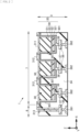
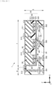
- a light emitting device 1 includes a substrate region 2, a light emitting body region 3, a color conversion region 4, a filter region 5, and an optical system region 6, in a vertical cross-section direction that is the arrowed Z direction.
- the light emitting device 1 includes a device arrangement region 7 and a peripheral region 8 in a planar direction including the arrowed X direction and the arrowed Y direction.
- the light emitting device 1 includes, as main components, a substrate 20 included in the substrate region 2, and a light emitting body 35 disposed in the light emitting body region 3 and including a plurality of light emitting elements 30 arranged in the device arrangement region 7.
- the substrate region 2 is configured to include the substrate 20 and a drive circuit 21 mounted on a main surface of the substrate 20.
- the main surface of the substrate 20 is one surface of the substrate 20 in which a semiconductor device such as a driving transistor is manufactured and the drive circuit 21 is formed.
- a monocrystalline silicon (Si) substrate is used, for example.
- An insulating body 201 is provided on a rear surface of the substrate 20 located on an opposite side from the main surface, and also on side surfaces.
- a silicon nitride (SiN) film or a silicon oxide (SiO) film may be practically used as the insulating body 201.
- the drive circuit 21 is configured with a semiconductor device provided at a main surface portion of the substrate 20.
- the semiconductor device includes a complementary insulated gate field effect transistor (IGFET) 23 as the driving transistor.
- the insulated gate field effect transistor 23 at least includes both a field effect transistor (MISFET) having a metal/insulating body/semiconductor structure and a field effect transistor (MOSFET) having a metal/oxide film/semiconductor structure.
- FIG. 1 illustrates an n-channel conductive type insulated gate field effect transistor 23.
- the insulated gate field effect transistor 23 is provided at the main surface portion of the substrate 20 in a region having a periphery surrounded by a device isolation region 22.
- a trench separation structure is used for the device isolation region 22. That is, the device isolation region 22 is configured to include a groove dug in a depth direction from the main surface of the substrate 20, and an insulating body embedded in the groove.
- the insulated gate field effect transistor 23 is configured to include a channel formation region (substrate 20), a gate insulating film 231, a gate electrode 232, and paired n-type semiconductor regions 233 used as a source region and a drain region.
- the gate insulating film 231 is provided on the channel formation region.
- the gate electrode 232 is provided on the gate insulating film 231.
- the paired n-type semiconductor regions 233 are provided at main surface portions of the substrate 20 that are spaced apart in a channel length direction with the channel formation region being interposed therebetween.
- insulated gate field effect transistors of a p-channel conductive type differ only in terms of the conductive type of the semiconductor region, and the basic structure is the same. Thus, illustration of the insulated gate field effect transistor of the p-channel conductive type and explanation of the structure thereof will not be provided.
- the drive circuit 21 is electrically coupled to each of a first terminal 281 and a second terminal 282 through a wiring layer 24.
- the wiring layer 24 includes a plug wiring line 241, a first layer wiring line 242, a second layer wiring line 243, a third layer wiring line 244, and a plug wiring line 245.
- the plug wiring line 241 is provided, for example, on the n-type semiconductor region 233 of the insulated gate field effect transistor 23, and one end (lower end) of the plug wiring line 241 is electrically coupled to the n-type semiconductor region 233.
- the plug wiring line 241 includes, for example, tungsten (W).
- the first layer wiring line 242 is provided on the plug wiring line 241, and the first layer wiring line 242 is electrically coupled to another end (upper end) of the plug wiring line 241.
- the second layer wiring line 243 is provided on the first layer wiring line 242, and the second layer wiring line 243 is electrically coupled to the first layer wiring line 242.
- the third layer wiring line 244 is provided on the second layer wiring line 243, and the third layer wiring line 244 is electrically coupled to the second layer wiring line 243.
- the first layer wiring line 242 to the third layer wiring line 244 each include, for example, aluminum (Al) as a main composition.
- an insulating body 25 is provided around the plug wiring line 241, between the first layer wiring line 242 and the second layer wiring line 243, between the second layer wiring line 243 and the third layer wiring line 244, and the like.
- the insulating body 25 includes, for example, a silicon oxide film or a silicon nitride film.
- the third layer wiring line 244 is electrically coupled to the first terminal 281 or the second terminal 282 sequentially through the plug wiring line 245, a second light shielding film 26, and a second light absorbing film 27.
- the second light shielding film 26 is disposed on the light emitting element 30 side of the insulated gate field effect transistor 23 that constitutes the drive circuit 21. Here, ends of the second light shielding film 26 extend in the planar direction to above the insulated gate field effect transistor 23.
- the second light shielding film 26 is disposed within the insulating body 25.
- the second light shielding film 26 blocks leakage light emitted from the light emitting element 30 toward the drive circuit 21 side, and is formed as an electrical path that electrically couples the drive circuit 21 and each of the first terminal 281 and the second terminal 282 to each other.
- the second light shielding film 26 includes a single metal layer film including, as a main composition, aluminum, copper (Cu), tungsten, or titanium (Ti), for example.
- the second light absorbing film 27 is disposed on the second light shielding film 26.
- the second light absorbing film 27 is formed to have the same planar shape as the planar shape of the second light shielding film 26 as viewed from a direction perpendicular to the main surface of the substrate 20 (hereinafter, simply referred to as "plan view").
- the second light absorbing film 27 is disposed within the insulating body 25.
- the second light absorbing film 27 absorbs leakage light emitted from the light emitting element 30 toward the drive circuit 21 side, and is formed as an electrical path that electrically couples the drive circuit 21 and each of the first terminal 281 and the second terminal 282 to each other.
- the second light absorbing film 27 includes a single layer film including metal or a metallic compound including, as a main composition, titanium (TiN), cobalt (Co), nitrogen-doped titanium oxide (TiON), tantalum nitride (TaN), or amorphous carbon (a-C), for example.
- TiN titanium
- Co cobalt
- TiON nitrogen-doped titanium oxide
- TaN tantalum nitride
- a-C amorphous carbon
- the first terminal 281 and the second terminal 282 are disposed on the second light absorbing film 27 and also on the insulating body 25. Each of the first terminal 281 and the second terminal 282 is electrically coupled to the second light absorbing film 27.
- the first terminal 281 is configured to be electrically coupled to one side (specifically, a first compound semiconductor layer 31) of the light emitting element 30.
- the second terminal 282 is configured to be electrically coupled to another side (specifically, a second compound semiconductor layer 32) of the light emitting element 30.
- the first terminal 281 and the second terminal 282 include the same conductive material, for example, copper (Cu).
- the light emitting body region 3 includes the light emitting body 35 disposed on the substrate region 2 and on the insulating body 25.
- a plurality of light emitting elements 30 is arranged in a matrix along directions (the arrowed X direction and the arrowed Y direction) of the light emitting surface of the light emitting elements 30.
- the plurality of light emitting elements 30 is formed from a singulated compound semiconductor layer.
- the light emitting element 30 formed from the singulated compound semiconductor layer is a light emitting element formed from a compound semiconductor layer obtained by causing a compound semiconductor layer to grow on a growth substrate, dicing the growth substrate and the compound semiconductor layer, and separating them into individual divided pieces. The growth substrate singulated together with the compound semiconductor layer is removed in a manufacturing process.
- one or a plurality of light emitting elements 30 is formed from the singulated compound semiconductor layer.
- the light emitting body 35 further includes an insulating body 34 provided around the plurality of light emitting elements 30 except for the light emitting surface.
- the insulating body 34 includes, as a main composition, a silicon oxide film or a silicon nitride film.
- the light emitting element 30 is configured as a light-emitting diode (LED) including the first compound semiconductor layer 31, the second compound semiconductor layer 32, and an active layer 33.
- the second compound semiconductor layer 32 is disposed on the substrate region 2 side.
- the light emitting element 30 includes, as a main composition, a III-V compound semiconductor, and the second compound semiconductor layer 32 includes, for example, a p-type gallium nitride (p-GaN).
- the first compound semiconductor layer 31 includes, for example, an n-type gallium nitride (n-GaN).
- a first light reflecting film 301 is provided for each of the plurality of light emitting elements 30.
- the first light reflecting film 301 is provided to surround the light emitting element 30 along side surfaces of the first compound semiconductor layer 31, side surfaces of the active layer 33, side surfaces of the second compound semiconductor layer 32, and a surface, on the substrate region 2 side, of the second compound semiconductor layer 32.
- the first light reflecting film 301 is not provided on the light emitting surface that is a surface of the first compound semiconductor layer 31.
- the first light reflecting film 301 reflects, toward the light emitting surface side, light emitted from the light emitting element 30, thereby improving light extraction efficiency.
- the first light reflecting film 301 has a constant film thickness along the side surfaces of the first compound semiconductor layer 31, the side surfaces of the active layer 33, the side surfaces of the second compound semiconductor layer 32, and the surface of the second compound semiconductor layer 32.
- the first light reflecting film 301 is formed by a chemical vapor deposition (CVD) method or an atomic layer deposition (ALD) method that provides favorable step coverage.
- CVD chemical vapor deposition
- ALD atomic layer deposition
- the first light reflecting film 301 includes, for example, metal such as aluminum or tungsten, or a metallic compound.
- a transparent electrode 311 is provided on the first compound semiconductor layer 31 of the light emitting element 30, and the transparent electrode 311 is electrically coupled to the first compound semiconductor layer 31.
- the transparent electrode 311 is integrally formed using the same conductive material in the light emitting elements 30 adjacent in a direction of the light emitting surface.
- the transparent electrode 311 is configured in the device arrangement region 7 as a common electrode shared between all the light emitting elements 30.
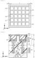
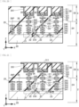
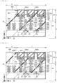
- the transparent electrode 311 has a rectangular shape in plan view, as illustrated in FIG. 4 .
- the transparent electrode 311 includes, for example, indium tin oxide (ITO).
- the transparent electrode 311 is electrically coupled to a first terminal 391 through a through wiring line 313.
- the through wiring line 313 is a wiring line extending in the thickness direction of the light emitting body 35 from the surface side of the light emitting body 35 toward the inside of the light emitting body 35. A specific material included in the through wiring line 313 will be described later.
- the first terminal 391 is provided at a surface, on the substrate region 2 side, of the light emitting body 35.
- the first terminal 391 is joined to and is electrically coupled to the first terminal 281.
- the first terminal 391 includes, for example, copper.
- a reflection attenuating film 312 is disposed on the transparent electrode 311 between the light emitting elements 30 to overlap with the transparent electrode 311.
- the reflection attenuating film 312 has a rectangular shape as a whole, as with the transparent electrode 311, and has a lattice shape extending in the arrowed X direction and the arrowed Y direction between the light emitting elements 30 as illustrated in FIG. 5 .
- the reflection attenuating film 312 is set such that a reflectance thereof at an interface with the transparent electrode 311 is lower than a light reflectance at an interface between the transparent electrode 311 and an insulting material of the insulating body 34.
- the reflection attenuating film 312 is formed such that a light transmittance thereof is lower than a light transmittance of the transparent electrode 311.
- the reflection attenuating film 312 has electrical conductivity, and is electrically coupled to the transparent electrode 311.
- the reflection attenuating film 312 includes a combined film including a titanium nitride film 312A and a tungsten film 312B stacked on the titanium nitride film 312A.
- the transparent electrode 311 is set to have a thickness of greater than or equal to 10 nm and less than or equal to 100 nm
- the titanium nitride film 312A is set to have a thickness of greater than or equal to 3 nm and less than or equal to 50 nm
- the tungsten film 312B is set to have a thickness of greater than or equal to 50 nm and less than or equal to 200 nm.
- the reflection attenuating film 312 may include a single layer film including, as a main composition, one or more metals selected from aluminum, titanium, tungsten, and copper, or may include a combined film including two or more layers. Furthermore, the reflection attenuating film 312 may include a metallic compound including the above-described metal as a main composition.
- the transparent electrode 311 and the reflection attenuating film 312 are electrically coupled to the through wiring line 313 in the peripheral region 8.
- the through wiring line 313 includes the same conductive material as the reflection attenuating film 312, and is provided at the same conductive layer. That is, in a method of manufacturing the light emitting device 1, the through wiring line 313 is formed through the same manufacturing processes as those for the reflection attenuating film 312.
- a transparent electrode 321 is provided on the surface, on the substrate region 2 side, of the second compound semiconductor layer 32 of the light emitting element 30.
- the transparent electrode 321 is electrically coupled to the second compound semiconductor layer 32.
- the transparent electrode 321 is configured for each of the light emitting elements 30 such that the periphery of the transparent electrode 321 is surrounded by the first light reflecting film 301, and has a rectangular shape in plan view, as with the transparent electrode 311.
- the transparent electrode 321 includes, for example, indium tin oxide, as with the transparent electrode 311.
- the transparent electrode 321 is electrically coupled to a second terminal 392 through a plug wiring line 36 provided directly below the transparent electrode 321 and for each of the light emitting elements 30.
- the plug wiring line 36 is a wiring line extending in the thickness direction of the light emitting body 35 from the surface side of the light emitting body 35 toward the inside of the light emitting body 35.
- One end portion of the plug wiring line 36 on the second compound semiconductor layer 32 side penetrates, in the thickness direction, through a portion of the first light reflecting film 301 provided along the second compound semiconductor layer 32, and is electrically coupled to the second compound semiconductor layer 32.
- Another end portion of the plug wiring line 36 on the substrate region 2 side is electrically coupled to the second terminal 392 with each of the first light absorbing film 37 and the first light shielding film 38 being interposed therebetween.
- the plug wiring line 36 is formed by filling, with an electrically conductive material, a contact hole, without reference character, formed in the insulating body 34. That is, in plan view, the dimension of one end portion of the plug wiring line 36 matches the dimension of an opening of the contact hole. In a portion of the first light reflecting film 301 where the plug wiring line 36 penetrates through, the first light reflecting film 301 and the plug wiring line 36 are only necessary to be electrically separated from each other. Thus, in plan view, it is possible to set the dimension of the opening to be small.
- the plug wiring line 36 includes, for example, tungsten.
- the second terminal 392 is provided at a position that corresponds to the second terminal 282 of the substrate region 2 at the surface of the light emitting body 35 on the substrate region 2 side.
- the second terminal 392 is joined to and is electrically coupled to the second terminal 282.
- the second terminal 392 includes, for example, copper, as with the first terminal 391.
- the first light absorbing film 37 is provided at an outer periphery intersecting with the direction (arrowed Z direction) in which the plug wiring line 36 extends, here, in a planar direction (the arrowed X direction and the arrowed Y direction) perpendicular to the direction (arrowed Z direction) in which the plug wiring line 36 extends.
- the first light absorbing film 37 is set to have the same dimension as the dimension of the opening of the portion of the first light reflecting film 301 where the plug wiring line 36 penetrates through, or to have a dimension larger than this dimension of the opening.
- the first light absorbing film 37 absorbs leakage light from a portion between the first light reflecting film 301 and the plug wiring line 36 toward the substrate region 2 side, and is formed as an electrical path that electrically couples the plug wiring line 36 and the second terminal 392 to each other.
- the first light absorbing film 37 is provided within the insulating body 25.
- the first light absorbing film includes, for example, the same electrically conductive material as the second light absorbing film.
- the first light shielding film 38 is provided below the first light absorbing film 37.
- the first light shielding film 38 has the same planar shape as the planar shape of the first light absorbing film 37 in plan view.
- the first light shielding film 38 is provided within the insulating body 25.
- the first light shielding film 38 blocks leakage light emitted from the light emitting element 30 toward the drive circuit 21 side, and is further formed as an electrical path, as with the first light absorbing film 37.
- the first light shielding film 38 includes, for example, the same electrically conductive material as the second light shielding film 26, and includes a single metal layer film including, for example, tungsten or cobalt as a main composition.
- the color conversion region 4 includes a color conversion layer 40 and a second light reflecting film 401.
- the color conversion layer 40 is provided on the light emitting surface of the light emitting element 30, in other word, is provided on the transparent electrode 311 with an insulating film 346 being interposed therebetween.
- the color conversion layer 40 is provided for each of the light emitting elements 30.
- the color conversion layer 40 converts light emitted from the light emitting element 30 into a particular color.
- the light emitting device 1 is configured as a color light emitting device (or a color image display apparatus).
- the color conversion layer 40 includes, for example, a resin material.
- the second light reflecting film 401 is provided along the periphery of side surfaces of the color conversion layer 40.
- the second light reflecting film 401 reflects light emitted from the light emitting element 30 and light diffused from the color conversion layer 40 to improve light extraction efficiency.
- the second light reflecting film 401 is formed, for example, using a method similar to that for the first light reflecting film 301, and includes, for example, the same material.
- the second light reflecting film 401 is separated from the reflection attenuating film 312 with an insulating film (no reference character is attached) being interposed therebetween.
- a separation wall 41 is provided at a portion that is between adjacent second light reflecting films 401 and is between the color conversion layers 40 adjacent in the planar direction.
- the separation wall 41 is configured to separate the color conversion layers 40 from each other, and hold the color conversion layers 40.
- the separation wall 41 includes, for example, a silicon oxide film or a silicon nitride film.
- the filter region 5 is provided on the color conversion region 4.
- the filter region 5 includes a filter 50.
- the filter 50 is provided on the color conversion layer 40, and blocks a particular emitted-light color emitted from the light emitting element 30 or absorbs the particular emitted-light color.
- the particular emitted-light color is, for example, blue.
- An optical system region 6 is provided on the filter region 5.
- An on-chip lens 60 is provided in the optical system region 6.
- the on-chip lens 60 includes a plurality of convex lenses that is integrally formed.
- the convex lenses are each disposed for corresponding one of the light emitting elements 30.
- the on-chip lens 60 includes, for example, a resin material or an inorganic material.
- a plurality of light emitting elements 30 is arranged in a matrix in the planar direction.
- the plurality of light emitting elements 30 is formed from the singulated compound semiconductor layer.
- the light emitting element 30 has a rectangular shape having a dimension of one side being greater than or equal to 0.5 ⁇ m and less than or equal to 20 ⁇ m, in plan view.
- the through wiring line 313 is disposed on the device arrangement region 7 side (inner side), and an external terminal 26P is provided on the outer side.
- one end of the through wiring line 313 is electrically coupled to the first compound semiconductor layer 31 of the light emitting element 30 through the transparent electrode 311 and the reflection attenuating film 312. Another end of the through wiring line 313 is electrically coupled to the drive circuit 21 through the joining portion of the first terminal 391 and the first terminal 281.
- the external terminal 26P is exposed from an opening extending from the filter region 5 into a portion of the substrate region 2.
- the external terminal 26P is electrically coupled to the drive circuit 21.
- the external terminal 26P is configured to allow a wire that is not illustrated in the drawing to be electrically coupled thereto. Through the wire, the external terminal 26P receives a drive signal that is inputted from the outside of the light emitting device 1 to the drive circuit 21.
- the external terminal 26P includes, for example, the same conductive material as the second light shielding film 26.
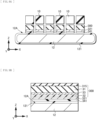
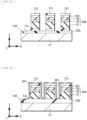
- a method of manufacturing the light emitting device 1 according to the first embodiment includes the following manufacturing processes illustrated in FIGs. 7 to 26 . Below, the method of manufacturing the light emitting device 1 will be described in detail.
- a compound semiconductor layer 300 is formed on a growth substrate 10 (see FIG. 7A ).
- a sapphire substrate is used as an epitaxial growth substrate.
- an undoped gallium nitride layer 315, the first compound semiconductor layer (n-GaN) 31, the active layer 33, and the second compound semiconductor layer (p-GaN) are formed sequentially from a surface of the growth substrate 10 (see FIG. 7B ).
- the transparent electrode 321 and an insulating film 341 are formed sequentially on the compound semiconductor layer 300.
- the growth substrate 10 is adhered to the dicing tape 11 (see FIG. 8 ).
- a dicing process is performed to dice the growth substrate 10, the compound semiconductor layer 300, the transparent electrode 321, and the insulating film 341 into individual singulated pieces.
- the singulated growth substrate 10 has a dimension of one side being greater than or equal to 4 mm and less than or equal to 30 mm.
- the singulated growth substrate 10, the singulated compound semiconductor layer 300, the singulated transparent electrode 321, and the singulated insulating film 341 are joined to a first joining surface 12A of a first support substrate 12 (see FIGs. 9A and 9B ).
- This joining is performed with the insulating film 341 and the first joining surface 12A of the first support substrate 12 being opposed to each other.
- a silicon substrate is used for the first support substrate 12, and an insulating film 121 is formed on the first joining surface 12A of the first support substrate 12.
- the insulating film 121 includes, for example, a silicon nitride film.
- the growth substrate 10 is peeled off.
- the undoped gallium nitride layer 315 of the compound semiconductor layer 300 is removed.
- the undoped gallium nitride layer 315 is removed, for example, through a polishing process.
- the insulating film 342 in which the plurality of singulated compound semiconductor layers 300 is embedded is formed on the first support substrate 12.
- the insulating film 342 includes, for example, a silicon oxide film. After this silicon oxide film is formed, a planarizing process is performed on the surface of this silicon oxide film.
- the planarizing process used includes, for example, a chemical mechanical polishing (CMP) process.
- a second support substrate 13 is prepared. As illustrated in FIG. 12 , the first joining surface 12A of the first support substrate 12 is opposed to a second joining surface 13A of the second support substrate 13 to join the first support substrate 12 to the second joining surface 13A. Through this joining, the directions of upward and downward of the compound semiconductor layer 300 is inverted. That is, the second compound semiconductor layer 32 is disposed at the upper layer of the compound semiconductor layer 300, and the first compound semiconductor layer 31 is disposed at the lower layer. For example, a plasma joining process is used for joining them.
- An insulating film 131 is formed in advance on the second joining surface 13A of the second support substrate 13.
- the insulating film 131 includes, for example, a silicon nitride film.
- FIG. 13B is an enlarged cross-sectional view of a region surrounded by a dashed line in FIG. 13A . Note that enlarged cross-sectional views illustrated in FIG. 14 and thereafter correspond to the enlarged cross-sectional view illustrated in FIG. 13B .
- the singulated compound semiconductor layer 300 is separated into individual pieces to form the plurality of light emitting elements 30.
- this process is a process of separating pixels from each other. Separating the compound semiconductor layer 300 is performed, for example, by a dry etching process.
- the thickness of the second compound semiconductor layer 32 is thinner, by approximately one digit, than the thickness of the first compound semiconductor layer 31.
- the accuracy of processing the active layer 33 is improved.
- the first light reflecting film 301 is formed along side surfaces of the light emitting element 30 and the surface of the second compound semiconductor layer 32.
- the first light reflecting film 301 is formed on the surface of the second compound semiconductor layer 32, except for a portion coupled to the plug wiring line 36. Note that, actually, the first light reflecting film 301 is formed on the surface of the insulating film 121.
- the first light reflecting film 301 is formed to have a constant film thickness using a chemical vapor deposition method or an atomic layer deposition method.
- an insulating film 343 is formed around the light emitting element 30 including the first light reflecting film 301, and the light emitting element 30 is embedded in the insulating film 343.
- the surface of the insulating film 343 is planarized, for example, by a chemical machine polishing process.
- the insulating film 343 includes, for example, a silicon oxide film.
- a contact hole (no reference character is attached) extending from the surface of the insulating film 343 and reaching the surface of the second compound semiconductor layer 32 of the light emitting element 30 is formed in the insulating film 343, and the plug wiring line 36 is formed in this contact hole (see FIG. 17 ).
- the plug wiring line 36 after the contact hole is first formed in the insulating film 343, a metal film for the plug wiring line 36 is formed in the contact hole and on the insulating film 343.
- the metal film is formed, for example, by using a chemical vapor deposition method that provides favorable step coverage.
- the metal film on the insulating film 343 is removed, for example, by a chemical mechanical polishing process, the metal film is left in the contact hole, and this metal film is formed as the plug wiring line 36.
- the first light absorbing film 37 and the first light shielding film 38 are formed sequentially on the plug wiring line 36 and the insulating film 343 (see FIG. 17 ). After the first light absorbing film 37 and the first light shielding film 38 are formed, an etching process is performed on them using a mask to process them into a predetermined shape.
- an insulating film 344 in which the first light absorbing film 37 and the first light shielding film 38 are embedded is formed, and the surface of the insulating film 344 is planarized.
- the insulating film 344 includes, for example, a silicon oxide film.
- the first terminal 391 is formed on the insulating film 344, and through the same manufacturing process, the second terminal 392 is formed in the device arrangement region 7.
- the first terminal 391 and the second terminal 392 each have an exposed surface, and the periphery of each of the first terminal 391 and the second terminal 392 is embedded in the insulating film 345.
- the surface of the first terminal 391, the surface of the second terminal 392, and the surface of the insulating film 345 are planarized by a chemical machine polishing process.
- the insulating film 341 to insulating film 345 constitute one insulating body 34, and the plurality of arranged light emitting elements 30 and the insulating body 34 formed around the light emitting elements 30 constitute the light emitting body 35 (see FIG. 1 ).
- the light emitting body 35 is formed, the light emitting body region 3 illustrated in FIG. 1 is substantially completed except for the transparent electrode 311 and the reflection attenuating film 312.
- the light emitting body region 3 is mounted on the substrate region 2 with the substrate 20 and the second support substrate 13 being opposed to each other, and the substrate region 2 and the light emitting body region 3 are joined together.
- the drive circuit 21 is mounted at the main surface portion of the substrate 20 of the substrate region 2. Furthermore, in the substrate region 2, the wiring layer 24, the second light shielding film 26, the second light absorbing film 27, the first terminal 281, and the second terminal 282 are formed on the substrate 20. Joining is performed in a state where the first terminal 391 of the light emitting body region 3 is electrically coupled to the first terminal 281 of the substrate region 2 and the second terminal 392 of the light emitting body region 3 is electrically coupled to the second terminal 282 of the substrate region 2.
- the second support substrate 13 is removed (see FIG. 20 ). Removing the second support substrate 13 is performed, for example, by a grinder process or a wet etching process.
- the insulating film 342 of the insulating body 34 is removed, and the surface of the first compound semiconductor layer 31 of the light emitting element 30 is exposed. Removing the insulating film 342 is performed by a dry etching process or a wet etching process.
- the transparent electrode 311 is formed on the first compound semiconductor layers 31 of the plurality of light emitting elements 30.
- a film including indium tin oxide is formed, for example, using sputtering or a vapor deposition method, and after the formation of the film, the film is processed into a predetermined shape by a wet etching process.
- the insulating film 346 is formed on the transparent electrode 311 (see FIG. 22 ).
- the insulating film 346 includes, for example, a silicon oxide film.
- an opening 346A is formed in the insulating film 346 between light emitting elements 30 in the device arrangement region 7.
- the opening 346A is formed, for example, by an etching process.
- an opening 346B extending from the surface of the insulating film 346 to the inside of the insulating body 34 is formed at a position, in the peripheral region 8, that corresponds to the first terminal 391.
- the surface of the first light absorbing film 37 on the first terminal 391 is exposed in the opening 346B.
- the reflection attenuating film 312 is formed on the insulating film 346 between light emitting elements 30.
- the reflection attenuating film 312 is electrically coupled to the transparent electrode 311 through the inside of the opening 346A.
- the through wiring line 313 is formed within the opening 346B in the peripheral region 8.
- the through wiring line 313 is electrically coupled to the second light shielding film 26 (corresponding to a first terminal according to the present disclosure) exposed in the opening 346B.
- the reflection attenuating film 312 and the through wiring line 313 are formed, for example, by a sputtering method, and is processed into a predetermined shape by a dry etching process.
- the separation wall 41 is formed between the light emitting elements 30 in the light emitting body region 3 ( FIG. 26 ).
- the separation wall 41 is formed by forming an insulating film on the entire region of the light emitting body region 3 that includes the device arrangement region 7 and the peripheral region 8 and removing the insulating film on the light emitting elements 30.
- the insulating film includes, for example, a silicon oxide film, and removing the insulating film is performed by a dry etching process.
- the second light reflecting film 401 is formed on side surfaces of the separation wall 41.
- the second light reflecting film 401 is formed by a chemical vapor deposition method or an atomic layer deposition method that provides favorable step coverage.
- the second light reflecting film 401 formed on the light emitting element 30 and the separation wall 41 are removed by an etch back process.
- the color conversion layer 40 is formed on the light emitting element 30 in a region of which side surfaces are surrounded by the separation wall 41.
- the color conversion layer 40 includes a resin material (see FIG. 26 ).
- a transparent resin layer 40A is formed on the light emitting element 30 serving as a sub-pixel.
- the color conversion region 4 is completed.
- the color conversion region 4 is not provided.
- the filter 50 is formed on the color conversion layer 40.
- the filter 50 blocks or absorbs a particular emitted-light color. Once the filter 50 is formed, the filter region 5 is completed.
- the on-chip lens 60 is formed on the filter region 5 (see FIG. 1 ). Once the on-chip lens 60 is formed, the optical system region 6 is completed.
- an opening 15 extending from the optical system region 6 and reaching the external terminal 26P of the substrate region 2 is formed in the peripheral region 8.
- the surface of the external terminal 26P is exposed in the opening 15.
- the method of manufacturing the light emitting device 1 according to the first embodiment ends, and the light emitting device 1 is completed.
- the light emitting body 35 such that the plurality of light emitting elements 30 manufactured from a plurality of growth substrates 10 are arranged, it is possible to join the light emitting body 35 to the substrate 20 having a size larger than that of the growth substrate 10, thereby forming the light emitting device 1 having a size as large as the size of the substrate 20.
- the light emitting element 30 includes the light-emitting diode including the first compound semiconductor layer 31, the second compound semiconductor layer 32, and the active layer 33. This makes it possible to achieve the increased size of the light emitting device 1 using the light-emitting diode as the light emitting element 30.
- the light emitting device 1 includes the first light reflecting film 301 as illustrated in FIGs. 1 and 2 .
- the first light reflecting film 301 is provided along the side surface of the first compound semiconductor layer 31, the side surface of the active layer 33, the side surface of the second compound semiconductor layer 32, and the surface, on the substrate 20 side, of the second compound semiconductor layer 32. This makes it possible to reflect the light emitted from the light emitting element 30 to guide it toward the light emitting surface, which makes it possible to improve the light extraction efficiency.
- the first light reflecting film 301 has the constant film thickness.
- the film thickness of the first light reflecting film 301 is reduced.
- the first light reflecting film 301 is provided along each of the side surfaces of the first compound semiconductor layer 31, the side surfaces of the active layer 33, and the side surfaces of the second compound semiconductor layer 32.
- the first light reflecting film 301 includes a metal film or a metallic compound film that is formed by a chemical vapor deposition method or an atomic layer deposition method.
- the first light reflecting film 301 exhibits favorable step coverage, which makes it possible to reduce the film thickness of the first light reflecting film 301 provided along each of the side surfaces of the first compound semiconductor layer 31, the side surfaces of the active layer 33, and the side surfaces of the second compound semiconductor layer 32. This makes it possible to dispose the first light reflecting film 301 around the side surfaces of the light emitting element 30 even if the spacing between adjacent light emitting elements 30 is reduced, which makes it possible to improve the light extraction efficiency.
- the light emitting device 1 further includes the transparent electrode 311 and the reflection attenuating film 312, as illustrated in FIGs. 1 to 5 .
- the transparent electrode 311 is disposed at the light emitting surface of the plurality of light emitting elements 30 and is provided integrally for the plurality of light emitting elements 30.
- the reflection attenuating film 312 is disposed on and overlaps with at least the transparent electrode 311 between the plurality of light emitting elements 30.
- the reflection attenuating film 312 has a reflectance at an interface between the reflection attenuating film 312 and the transparent electrode 311 that is lower than a reflectance of the transparent electrode 311 at an interface between the transparent electrode 311 and an insulating material.
- leakage light LL emitted from the light emitting element 30 is attenuated at the time of being reflected at the interface between the transparent electrode 311 and the reflection attenuating film 312, in a process in which the leakage light LL is transmitted through the inside of the transparent electrode 311 to other adjacent light emitting elements 30. This makes it possible to attenuate leakage light between adjacent light emitting elements 30.
- the reflection attenuating film 312 has electrical conductivity, and is electrically coupled to the transparent electrode 311. That is, the reflection attenuating film 312 is provided as a wiring line that reduces a resistance value of the transparent electrode 311. As the resistance value of the transparent electrode 311 is allowed to be reduced, it is possible to reduce the film thickness of the transparent electrode 311. This reduces the cross sectional area of a path of leakage light of the transparent electrode 311, which makes it possible to further reduce the leakage light between the light emitting elements 30.
- the reflection attenuating film 312 extends to the peripheral region 8 of the light emitting body 35.
- the reflection attenuating film 312 is electrically coupled to the first terminal 391 or the first terminal 281 through the through wiring line 313.
- the through wiring line 313 penetrates the insulating body 34 and includes a conductive material same as that of the reflection attenuating film 312.
- the through wiring line 313 is electrically coupled to the second light shielding film 26 used as the first terminal.
- the reflection attenuating film 312 including the same conductive material (or using the same manufacturing processes) as the through wiring line 313 by using the through wiring line 313 formed in the peripheral region 8. This makes it possible to easily provide the reflection attenuating film 312.
- the reflection attenuating film 312 illustrated in FIGs. 1 to 3 and 5 includes a single layer film or a combined film that includes one or more materials selected from tungsten, aluminum, titanium, tantalum, copper, and titanium nitride. That is, the reflection attenuating film 312 includes an existing material having high stability and high reliability, which makes it possible to easily form the reflection attenuating film 312.
- the light emitting device 1 includes the color conversion layer 40 and the second light reflecting film 401 as illustrated in FIG. 1 .
- the color conversion layer 40 is disposed on the light emitting surface for each of the plurality of light emitting elements 30.
- the second light reflecting film 401 is disposed around a side surface of the color conversion layer 40, and reflects light emitted from the plurality of light emitting elements 30 and light scattered by the color conversion layer 40.
- the on-chip lens 60 is provided as an optical lens on the color conversion layer 40. Providing the on-chip lens 60 makes it possible to improve a property of collecting extracted light.
- the light emitting device 1 includes the plug wiring line 36 as illustrated in FIGs. 1 and 2 .
- One end surface of the plug wiring line 36 in an extending direction penetrates the first light reflecting film 301 in a thickness direction and is electrically coupled to the surface, on the substrate 20 side, of the second compound semiconductor layer 32 of the plurality of light emitting elements 30.
- Another end surface of the plug wiring line 36 in the extending direction is electrically coupled to the second terminal 392 or the second terminal 282. It is possible to couple the plug wiring line 36 to the second compound semiconductor layer 32 at the dimension that is the same as the opening dimension of the contact hole formed in the insulating film 343 illustrated in FIG. 17 . That is, the area where the plug wiring line 36 and the second compound semiconductor layer 32 are coupled to each other is reduced.
- the plug wiring line 36 and the first light reflecting film 301 are electrically separated from each other.
- the spacing between the plug wiring line 36 and the first light reflecting film 301 is reduced. This makes it possible to reduce leakage light emitted from the light emitting element 30 toward the substrate 20 side.
- the light emitting device 1 includes the first light absorbing film 37 as illustrated in FIGs. 1 and 2 .
- the first light absorbing film 37 is provided at the outer periphery between the first light reflecting film 301 and the second terminal 392 or the second terminal 282.
- the outer periphery intersects with the extending direction of the plug wiring line 36.
- the first light absorbing film 37 absorbs leakage light from between the first light reflecting film 301 and the plug wiring line 36 toward the substrate 20 side. This makes it possible to reduce the leakage light emitted from the light emitting element 30 toward the substrate 20 side.
- the first light absorbing film 37 illustrated in FIGs. 1 and 2 includes titanium nitride, cobalt, nitrogen-doped titanium oxide, tantalum nitride, or amorphous carbon.
- the first light absorbing film 37 includes a material having high light absorptance, it is possible to further reduce the leakage light emitted from the light emitting element 30 toward the substrate 20 side.
- the light emitting device 1 includes the first light shielding film 38 as illustrated in FIGs. 1 and 2 .
- the first light shielding film 38 is provided at the outer periphery between the first light reflecting film 301 and the second terminal 392 or the second terminal 282.
- the outer periphery intersects with the extending direction of the plug wiring line 36.
- the first light shielding film 38 blocks leakage light from between the first light reflecting film 301 and the plug wiring line 36 toward the substrate 20 side. This makes it possible to reduce the leakage light emitted from the light emitting element 30 toward the substrate 20 side.
- the first light shielding film 38 illustrated in FIGs. 1 and 2 is provided to include aluminum, copper, tungsten, or titanium. Because the first light shielding film 38 includes a material having a high light reflectance, it is possible to further reduce the leakage light emitted from the light emitting element 30 toward the substrate 20 side.
- the drive circuit 21 includes the insulated gate field effect transistor 23 serving as the driving transistor, as illustrated in FIG. 1 .
- the light emitting device 1 includes the second light shielding film 26 and the second light absorbing film 27 on the side of the plurality of light emitting elements 30 with respect to the insulated gate field effect transistor 23.
- the second light shielding film 26 blocks leakage light from the plurality of light emitting elements 30 toward the substrate 20 side.
- the second light absorbing film 27 absorbs the leakage light from the plurality of light emitting elements 30 toward the substrate 20 side.
- the second light shielding film 26 illustrated in FIG. 1 is provided to include aluminum, copper, tungsten, or titanium.
- the second light shielding film 26 includes a material having a high light reflectance, it is possible to further reduce the leakage light emitted from the light emitting element 30 toward the substrate 20 side.
- the compound semiconductor layer 300 is formed as illustrated in FIGs. 7A and 7B .
- the compound semiconductor layer 300 is obtained by causing the first compound semiconductor layer 31, the active layer 33, and the second compound semiconductor layer 32 to sequentially grow on the growth substrate 10.
- the singulated compound semiconductor layer 300 is formed by dicing the growth substrate 10 and the compound semiconductor layer 300.
- the second compound semiconductor layer 32 is caused to be opposed to the first joining surface 12A of the first support substrate 12, and the compound semiconductor layer 300 is joined to the first joining surface 12A (see FIGs. 9A and 9B ).
- the growth substrate 10 is peeled off.
- FIG. 9A and 9B the growth substrate 10 is peeled off.
- the first compound semiconductor layer 31 is caused to be opposed to the second joining surface 13Aof the second support substrate 13, and the compound semiconductor layer 300 is joined to the second joining surface 13A.
- the first support substrate 12 is removed.
- the plurality of light emitting elements 30 is formed from the singulated compound semiconductor layer 300.
- the light emitting body 35 is formed by forming the insulating body 34 around the plurality of light emitting elements 30 on the second support substrate 13. As illustrated in FIG.
- the second support substrate is joined to the substrate 20 on which the drive circuit 21, to which the second light shielding film 26 as the first terminal (or the first terminal 281) and the second terminal 282 are coupled, is mounted, in a state where the light emitting body 35 is interposed between the substrate 20 and the second support substrate and the second compound semiconductor layer 32 is electrically coupled to the second terminal 282.
- the second support substrate 13 is removed.
- the first compound semiconductor layer 31 and the second light shielding film 26 are electrically coupled to each other.
- the plurality of light emitting elements 30 is formed from the singulated compound semiconductor layer 300 (see FIG. 8 ), and the insulating body 34 is formed around the plurality of light emitting elements 30 to form the light emitting body 35.
- the light emitting body 35 is joined to the substrate 20, it is possible to increase the size of the substrate 20 at which the drive circuit 21 is mounted, regardless of the size of the growth substrate 10 (see FIGs. 7A and 7B ) from which the light emitting elements 30 are manufactured.
- the light emitting elements 30 manufactured from the growth substrate 10 having a size of 4 inches to 6 inches are mounted on the substrate 20 having, for example, a size of 8 inches to 12 inches. This makes it possible to manufacture the light emitting device 1 having a size as large as the size of the substrate 20.
- the singulated compound semiconductor layer 300 is processed in a state of being joined to the second support substrate 13, to form the light emitting elements 30.
- the second support substrate 13 is joined to the substrate 20, and the light emitting element 30 is mounted on the substrate 20. Because the second support substrate 13 and the substrate 20 are each in a state of being a wafer, wafers are joined to each other. This makes it possible to improve accuracy of alignment at the time of joining.
- the transparent electrode 311 is formed at the light emitting surface of the plurality of light emitting elements 30 after the second support substrate 13 is removed.
- the reflection attenuating film 312 is formed on the transparent electrode 311 between the plurality of light emitting elements 30 in the same process as the process of coupling the first compound semiconductor layer 31 and the first terminal 391 to each other.
- the reflection attenuating film 312 has a reflectance at an interface between the reflection attenuating film 312 and the transparent electrode 311 that is lower than a reflectance of the transparent electrode 311 at an interface between the transparent electrode 311 and an insulating material.
- the reflection attenuating film 312 is formed in the same process as the process of coupling the first compound semiconductor layer 31 and the first terminal 391 to each other, specifically, as the manufacturing process of forming the through wiring line 313. This makes it possible to reduce the number of manufacturing processes, as compared with a case where the reflection attenuating film 312 is formed through a different manufacturing process.
- the light emitting device 1 includes a through wiring line 361 that couples the first compound semiconductor layer 31 of the light emitting element 30 and the first terminal 391 to each other, as illustrated in FIG. 27 .
- the upper end of the through wiring line 361 is electrically coupled to the reflection attenuating film 312 extending from the device arrangement region 7 to the peripheral region 8.
- the through wiring line 361 includes the same electrically conductive material as the plug wiring line 36 that electrically couples the second compound semiconductor layer 32 and the second terminal 392 to each other.
- the through wiring line 361 is formed through a manufacturing process that is the same as the process of manufacturing the plug wiring line 36.
- the light emitting device 1 according to the second embodiment makes it possible to achieve workings and effects similar to the workings and effects achievable by the light emitting device 1 according to the first embodiment.
- the light emitting device 1 includes the through wiring line 361 as illustrated in FIG. 27 . Because the through wiring line 361 includes the same electrically conductive material as the plug wiring line 36, it is possible to easily achieve the structure of coupling the first compound semiconductor layer 31 of the light emitting element 30 and the first terminal 391 to each other.
- the light emitting device 1 includes the reflection attenuating film 312 on the transparent electrode 311 between the light emitting elements 30 as illustrated in FIG. 28 .
- the entire lower surface of the reflection attenuating film 312 is joined to the transparent electrode 311 without the insulating film 346 being interposed therebetween.
- the reflection attenuating film 312 according to the third embodiment makes it possible to increase the area in which the transparent electrode 311 is joined. This makes it possible to further reduce the resistance value of the transparent electrode 311, and also makes it possible to reduce the film thickness of the transparent electrode 311.
- the light emitting device 1 according to the fourth embodiment of the present technology includes the reflection attenuating film 312 on the transparent electrode 311 between the light emitting elements 30 as illustrated in FIG. 29 .
- the light emitting device 1 according to the fourth embodiment is a modification example of the light emitting device 1 according to the third embodiment, and the reflection attenuating film 312 is coupled to the second light reflecting film 401 of the color conversion region 4.
- the second light reflecting film 401 is coupled to the transparent electrode 311 with the reflection attenuating film 312 being interposed therebetween.
- the second light reflecting film 401 and the transparent electrode 311 are kept at the same electric potential.
- the light emitting device 1 according to the fifth embodiment of the present technology includes the reflection attenuating film 312 on the transparent electrode 311 between the light emitting elements 30 as illustrated in FIG. 30 .
- the light emitting device 1 according to the fifth embodiment is a modification example of the light emitting device 1 according to the third embodiment, and the reflection attenuating film 312 penetrates through the transparent electrode 311, and is coupled to the first light reflecting film 301 provided around the light emitting element 30.
- the first light reflecting film 301 is coupled to the transparent electrode 311 with the reflection attenuating film 312 being interposed therebetween.
- the first light reflecting film 301 and the transparent electrode 311 are kept at the same electric potential.
- a portion of the reflection attenuating film 312 is formed to penetrate through the transparent electrode 311 in the thickness direction as illustrated in FIG. 30 .
- the leakage light transmitted to the inside of the transparent electrode 311 is blocked by a portion of the reflection attenuating film 312. This makes it possible to further reduce the leakage light.
- the light emitting device 1 according to the sixth embodiment of the present technology includes the reflection attenuating film 312 on the transparent electrode 311 between the light emitting elements 30 as illustrated in FIG. 31 .
- the light emitting device 1 according to the sixth embodiment is a modification example combining the light emitting device 1 according to the fourth embodiment and the light emitting device 1 according to the fifth embodiment. That is, the reflection attenuating film 312 penetrates through the transparent electrode 311 to be coupled to the first light reflecting film 301 disposed around the light emitting elements 30, and is also coupled to the second light reflecting film 401 of the color conversion region 4.
- the first light reflecting film 301 and the second light reflecting film 401 are coupled to the transparent electrode 311 with the reflection attenuating film 312 being interposed therebetween.
- the first light reflecting film 301 and the second light reflecting film 401 are each kept at the same electric potential as the transparent electrode 311.
- the light emitting elements 30 formed from the singulated compound semiconductor layer 300 is not separated for each pixel, as illustrated in FIG. 32 .
- a portion between adjacent light emitting elements 30 is cut from the second compound semiconductor layer 32 beyond the active layer 33 up to some middle point of the first compound semiconductor layer 31, and is separated.
- the first compound semiconductor layers 31 adjacent to each other are coupled to each other.
- the adjacent light emitting elements 30 be separated from each other. However, if the spacing (pixel pitch) between the adjacent light emitting elements 30 is large enough to make the color mixture negligible, the light emitting elements 30 may not be separated from each other.
- a position at which the plug wiring line 36 and the first light absorbing film 37 are coupled to each other is offset relative to the position at which the first light shielding film 38 and the second terminal 392 are coupled to each other. This makes it possible to block a path of the leakage light from the light emitting element 30 toward the substrate 20 side, which makes it possible to further reduce leakage holes.
- the light emitting device 1 according to the eighth embodiment of the present technology is a modification example of the light emitting device 1 according to the seventh embodiment.
- the light emitting device 1 includes a separation region 305 between the adjacent light emitting elements 30 as illustrated in FIG. 33 . Between the light emitting elements 30, the separation region 305 is provided from the second compound semiconductor layer 32 beyond the active layer 33 up to some middle point of the first compound semiconductor layer 31.
- the separation region 305 is formed, for example, by implanting ions using an ion implantation method and insulating a portion of the compound semiconductor layer 300.
- the light emitting device 1 according to the eighth embodiment makes it possible to achieve workings and effects similar to the workings and effects achievable by the light emitting device 1 according to the seventh embodiment.
- the light emitting device 1 according to the ninth embodiment of the present technology is a modification example in which the light shielding structure of the light emitting device 1 according to the first embodiment is modified.
- the light emitting device 1 includes a second light shielding film 271 on the insulated gate field effect transistor 23 that constitutes the drive circuit 21.
- the second light shielding film 271 covers the insulated gate field effect transistor 23.
- the second light shielding film 271 blocks the leakage light from the light emitting element 30 toward the insulated gate field effect transistor 23, as with the second light shielding film 26 of the light emitting device 1 according to the first embodiment.
- the light emitting device 1 includes a first light shielding film 381 between the second compound semiconductor layer 32 of the light emitting element 30 and the plug wiring line 36.
- a middle portion of the first light shielding film 381 is coupled to the second compound semiconductor layer 32 and the plug wiring line 36.
- the light emitting device 1 includes the through wiring line (plug wiring line) 361 between the light emitting elements 30.
- the through wiring line 361 electrically couples the first compound semiconductor layer 31 and the first terminal 391 to each other.
- a first light shielding film 382 having a structure similar to that of the first light shielding film 381 is provided at a portion at which the first compound semiconductor layer 31 and the through wiring line 361 are coupled to each other.
- the light emitting device 1 according to the ninth embodiment makes it possible to achieve workings and effects similar to the working and effects achievable by the light emitting device 1 according to the first embodiment.
- the light emitting device 1 includes the first light shielding film 381, the first light shielding film 382, and the second light shielding film 271. This makes it possible to effectively block the path of the leakage light from the light emitting element 30 toward the substrate 20, which makes it possible to further reduce the leakage light.
- FIG. 35 is an elevation view of one example of an appearance of a digital still camera (electronic apparatus) 1310.
- FIG. 36 is a back view of one example of the appearance of the digital still camera 1310.
- This digital still camera 1310 is of a lens-exchangeable single-lens reflex type.
- the digital still camera 1310 includes an exchangeable image-capturing lens unit (interchangeable lens) 1312 at substantially the middle of a camera body portion (camera body) 1311 as viewed from the front, and also includes a grip portion 1313 disposed at the left side as viewed from the front.
- the grip portion 1313 is to be held by a photographer.
- a monitor 1314 is provided at a position shifted toward the left side from the middle of the camera body portion 1311 as viewed from the back.
- An electronic viewfinder (eyepiece window) 1315 is provided above the monitor 1314. By looking into the electronic viewfinder 1315, the photographer visually recognizes an optical image of a subject that is guided from the image-capturing lens unit 1312, thereby being able to determine the composition.
- the electronic viewfinder 1315 includes the light emitting device 1.
- FIG. 37 is a perspective view of one example of an appearance of a head-mounted display (electronic apparatus) 1320.
- the head-mounted display 1320 includes, for example, temples 1322 disposed at both sides of an eyeglass-shaped displaying unit 1321.
- the temples 1322 allows for mounting on the user's head.
- the displaying unit 1321 includes the light emitting device 1.
- FIG. 38 is a perspective view of one example of an appearance of a television apparatus (electronic apparatus) 1330.
- This television apparatus 1330 includes, for example, an image display screen unit 1331 including a front panel 1332 and a filter glass 1333.
- the image display screen unit 1331 includes the light emitting device 1.
- the present technology is not limited to the embodiments described above, and various modifications are possible without departing from the gist of the present technology. For example, it is possible to combine two or more of the embodiments described above.
- the present technology may be applied to a single-color light emitting device that does not include any color conversion region and a method of manufacturing the light emitting device.
- a plurality of light emitting elements formed from a singulated compound semiconductor layer is arranged in a row direction and a column direction.
- the plurality of light emitting elements is embedded in an insulating body except for a light emitting surface, and a light emitting body is thus provided.
- the light emitting body is joined to a substrate including a drive circuit, a first terminal, and a second terminal.
- the first terminal and the second terminal electrically couple the drive circuit and the plurality of light emitting elements to each other.
- the light emitting device is thus manufactured. This eliminates restriction in terms of the size of a substrate on which the drive circuit is mounted due to the size of the growth substrate of the light emitting elements. This makes it possible to achieve an increase in the size of the light emitting device.
- the present technology includes the following configurations.
Landscapes
- Physics & Mathematics (AREA)
- General Physics & Mathematics (AREA)
- Engineering & Computer Science (AREA)
- Theoretical Computer Science (AREA)
- Led Device Packages (AREA)
- Led Devices (AREA)
Abstract
Description
- The present disclosure relates to a light emitting device and a method of manufacturing a light emitting device.
-
PTL 1 discloses an image display element and a method of manufacturing the same. The image display element is configured such that a plurality of micro light emitting elements is arranged on a drive circuit substrate in a two-dimensional array shape. The micro light emitting element is a light-emitting diode (LED) including a compound semiconductor. - In a method of manufacturing the image display element, a compound semiconductor is formed on a growth substrate through epitaxial growth. The compound semiconductor is divided into a plurality of pieces on the growth substrate, and electrodes and the like are formed at the plurality of compound semiconductors to form a plurality of micro light emitting elements. In addition, the growth substrate is caused to be opposed to the drive circuit substrate, and the plurality of micro light emitting elements on the growth substrate is joined to the drive circuit substrate. After they are joined, the growth substrate is removed.
- PTL 1:
Japanese Unexamined Patent Application Publication No. 2020-88383 - Incidentally, crystal defects are more likely to occur at a compound semiconductor formed through epitaxial growth. Thus, from the viewpoint of yielding during manufacturing, a small-sized growth substrate is used. For example, a growth substrate having a size equal to or less than 6 inches is used. Thus, it is desired to develop a large-sized light emitting device having a size larger than that of the growth substrate.
- The present disclosure provides a light emitting device that makes it possible to achieve an increase in size, and a method of manufacturing the light emitting device.
- A light emitting device according to an embodiment of the present disclosure includes a light emitting body and a substrate. The light emitting body includes a plurality of light emitting elements and an insulating body in which the plurality of light emitting elements is embedded except for a light emitting surface of the plurality of light emitting elements. The plurality of light emitting elements is formed from a singulated compound semiconductor layer and is arranged in a row direction and a column direction. The substrate includes a drive circuit, a first terminal, and a second terminal and is joined to the light emitting body. The drive circuit drives the plurality of light emitting element. The first terminal and the second terminal electrically couple the drive circuit and the plurality of light emitting element to each other.
- A method of manufacturing a light emitting device according to an embodiment of the present disclosure includes: forming a compound semiconductor layer obtained by causing a first compound semiconductor layer, an active layer, and a second compound semiconductor layer to sequentially grow on a growth substrate; forming a singulated compound semiconductor layer by dicing the growth substrate and the compound semiconductor layer; causing the second compound semiconductor layer to be opposed to a first joining surface of a first support substrate and joining the compound semiconductor layer to the first joining surface; peeling off the growth substrate; causing the first compound semiconductor layer to be opposed to a second joining surface of a second support substrate and joining the compound semiconductor layer to the second joining surface; removing the first support substrate; forming a plurality of light emitting elements from the singulated compound semiconductor layer; forming a light emitting body by forming an insulating body around the plurality of light emitting elements on the second support substrate; joining the second support substrate to a substrate on which a drive circuit, to which a first terminal and a second terminal are coupled, is mounted, in a state where the light emitting body is interposed between the substrate and the second support substrate and the second compound semiconductor layer is electrically coupled to the second terminal; removing the second support substrate; and electrically coupling the first compound semiconductor layer and the first terminal to each other.
-
- [
FIG. 1] FIG. 1 is a schematic cross-sectional view of a light emitting device according to a first embodiment of the present disclosure. - [
FIG. 2] FIG. 2 is an enlarged cross-sectional view in which a main part of the light emitting device illustrated inFIG. 1 is enlarged. - [
FIG. 3] FIG. 3 is an enlarged main-part cross-sectional view in which a part between light emitting elements of the light emitting device illustrated inFIG. 2 is further enlarged. - [
FIG. 4] FIG. 4 is a plan view of a transparent electrode of the light emitting device illustrated inFIGs. 1 and2 . - [
FIG. 5] FIG. 5 is a plan view of a reflection attenuating film corresponding toFIG. 4 of the light emitting device illustrated inFIGs. 1 and2 . - [
FIG. 6] FIG. 6 is an enlarged cross-sectional view in which a main part of the light emitting device illustrated inFIG. 1 is enlarged. - [
FIG. 7A] FIG. 7A is a cross-sectional view of a first process, describing a method of manufacturing the light emitting device according to the first embodiment. - [
FIG. 7B] FIG. 7B is a cross-sectional view in which a main part of the cross-sectional view of the first process illustrated inFIG. 7A is enlarged. - [
FIG. 8] FIG. 8 is a cross-sectional view of a second process. - [
FIG. 9A] FIG. 9A is a cross-sectional view of a third process. - [
FIG. 9B] FIG. 9B is a cross-sectional view in which a main part of the cross-sectional view of the third process illustrated inFIG. 9A is enlarged. - [
FIG. 10A] FIG. 10A is a cross-sectional view of a fourth process. - [
FIG. 10B] FIG. 10B is a cross-sectional view in which a main part of the cross-sectional view of the fourth process illustrated inFIG. 10A is enlarged. - [
FIG. 11] FIG. 11 is a cross-sectional view of a fifth process. - [
FIG. 12] FIG. 12 is a cross-sectional view of a sixth process. - [
FIG. 13A] FIG. 13A is a cross-sectional view of a seventh process. - [
FIG. 13B] FIG. 13B is a cross-sectional view in which a main part of the cross-sectional view of the seventh process illustrated inFIG. 13A is enlarged. - [
FIG. 14] FIG. 14 is a cross-sectional view of an eighth process, corresponding toFIG. 7B . - [
FIG. 15] FIG. 15 is a cross-sectional view of a ninth process, corresponding toFIG. 7B . - [
FIG. 16] FIG. 16 is a cross-sectional view of a tenth process, corresponding toFIG. 7B . - [
FIG. 17] FIG. 17 is a cross-sectional view of an eleventh process, corresponding toFIG. 7B . - [
FIG. 18] FIG. 18 is a cross-sectional view of a twelfth process, corresponding toFIG. 7B . - [
FIG. 19] FIG. 19 is a cross-sectional view of a thirteenth process, corresponding toFIG. 7B . - [
FIG. 20] FIG. 20 is a cross-sectional view of a fourteenth process, corresponding toFIG. 7B . - [
FIG. 21] FIG. 21 is a cross-sectional view of a fifteenth process, corresponding toFIG. 7B . - [
FIG. 22] FIG. 22 is a cross-sectional view of a sixteenth process, corresponding toFIG. 7B . - [
FIG. 23] FIG. 23 is a cross-sectional view of a seventeenth process, corresponding toFIG. 7B . - [
FIG. 24] FIG. 24 is a cross-sectional view of an eighteenth process, corresponding toFIG. 7B . - [
FIG. 25] FIG. 25 is a cross-sectional view of a nineteenth process, corresponding toFIG. 7B . - [
FIG. 26] FIG. 26 is a cross-sectional view of a twentieth process, corresponding toFIG. 7B . - [
FIG. 27] FIG. 27 is an enlarged cross-sectional view of a light emitting device according to a second embodiment of the present disclosure, corresponding toFIG. 2 . - [
FIG. 28] FIG. 28 is an enlarged main-part cross-sectional view of a light emitting device according to a third embodiment of the present disclosure, corresponding toFIG. 3 . - [
FIG. 29] FIG. 29 is an enlarged main-part cross-sectional view of a light emitting device according to a fourth embodiment of the present disclosure, corresponding toFIG. 3 . - [
FIG. 30] FIG. 30 is an enlarged main-part cross-sectional view of a light emitting device according to a fifth embodiment of the present disclosure, corresponding toFIG. 3 . - [
FIG. 31] FIG. 31 is an enlarged main-part cross-sectional view of a light emitting device according to a sixth embodiment of the present disclosure, corresponding toFIG. 3 . - [
FIG. 32] FIG. 32 is an enlarged cross-sectional view of a light emitting device according to a seventh embodiment of the present disclosure, corresponding toFIG. 2 . - [
FIG. 33] FIG. 33 is an enlarged cross-sectional view of a light emitting device according to an eighth embodiment of the present disclosure, corresponding toFIG. 2 . - [
FIG. 34] FIG. 34 is an enlarged cross-sectional view of a light emitting device according to a ninth embodiment of the present disclosure, corresponding toFIG. 6 . - [
FIG. 35] FIG. 35 is an elevation view of an example of an appearance of a digital still camera which is a first application example of the light emitting device of the present disclosure. - [
FIG. 36] FIG. 36 is a back view of an example of the appearance of the digital still camera illustrated inFIG. 35 . - [
FIG. 37] FIG. 37 is a perspective view of an example of an appearance of a head-mounted display which is a second application example of the light emitting device of the present disclosure. - [
FIG. 38] FIG. 38 is a perspective view of an example of an appearance of a television apparatus which is a third application example of the light emitting device of the present disclosure. - Below, embodiments according to the present disclosure will be described in detail with reference to the drawings. Note that the description will be given in the following order.
- A first embodiment is an example in which the present technology is applied to a light emitting device and a method of manufacturing the light emitting device.
- A second embodiment is an example in which a structure of coupling a light emitting element and a drive circuit in the light emitting device according to the first embodiment is modified.
- Third to sixth embodiments are examples in which a structure of a reflection attenuating film disposed between light emitting elements in the light emitting device according to the first embodiment is modified.
- Seventh and eighth embodiments are examples in which a separation structure of the light emitting element in the light emitting device according to the first embodiment is modified.
- A ninth embodiment is an example in which a structure of a light shielding film in the light emitting device according to the first embodiment is modified.
- A first application example is an example in which the present technology is applied to a digital still camera. A second application example is an example in which the present technology is applied to a head-mounted display. A third application example is an example in which the present technology is applied to a television apparatus.
- Here, an arrowed X direction illustrated in the drawings on an as-necessary basis is one direction of a planar direction of a light emitting device, directed from the left side on a paper surface toward the right side. An arrowed Y direction is perpendicular to the arrowed X direction and is another direction of the planar direction of the light emitting device, directed from the paper surface front side toward a direction going behind the paper surface. In addition, an arrowed Z direction is perpendicular to the arrowed X direction and the arrowed Y direction, and is a height direction of the light emitting device from the bottom side of the paper surface toward the upper side. The arrowed X direction, the arrowed Y direction, and the arrowed Z direction correspond to an X-axis direction, a Y-axis direction, and a Z-axis direction, respectively, in a three-dimensional coordinate system.
- Note that these directions are illustrated to help understand the present technology, and are not given for the purpose of limiting the direction of the present technology.
- As illustrated in
FIG. 1 , alight emitting device 1 according to the first embodiment of the present technology includes asubstrate region 2, a light emittingbody region 3, acolor conversion region 4, afilter region 5, and anoptical system region 6, in a vertical cross-section direction that is the arrowed Z direction. In addition, thelight emitting device 1 includes adevice arrangement region 7 and aperipheral region 8 in a planar direction including the arrowed X direction and the arrowed Y direction. - Furthermore, the
light emitting device 1 includes, as main components, asubstrate 20 included in thesubstrate region 2, and alight emitting body 35 disposed in the light emittingbody region 3 and including a plurality oflight emitting elements 30 arranged in thedevice arrangement region 7. - The
substrate region 2 is configured to include thesubstrate 20 and adrive circuit 21 mounted on a main surface of thesubstrate 20. Here, the main surface of thesubstrate 20 is one surface of thesubstrate 20 in which a semiconductor device such as a driving transistor is manufactured and thedrive circuit 21 is formed. - For the
substrate 20, a monocrystalline silicon (Si) substrate is used, for example. An insulatingbody 201 is provided on a rear surface of thesubstrate 20 located on an opposite side from the main surface, and also on side surfaces. For example, a silicon nitride (SiN) film or a silicon oxide (SiO) film may be practically used as the insulatingbody 201. - The
drive circuit 21 is configured with a semiconductor device provided at a main surface portion of thesubstrate 20. The semiconductor device includes a complementary insulated gate field effect transistor (IGFET) 23 as the driving transistor. The insulated gatefield effect transistor 23 at least includes both a field effect transistor (MISFET) having a metal/insulating body/semiconductor structure and a field effect transistor (MOSFET) having a metal/oxide film/semiconductor structure. -
FIG. 1 illustrates an n-channel conductive type insulated gatefield effect transistor 23. The insulated gatefield effect transistor 23 is provided at the main surface portion of thesubstrate 20 in a region having a periphery surrounded by adevice isolation region 22. For example, a trench separation structure ( is used for thedevice isolation region 22. That is, thedevice isolation region 22 is configured to include a groove dug in a depth direction from the main surface of thesubstrate 20, and an insulating body embedded in the groove. - The insulated gate
field effect transistor 23 is configured to include a channel formation region (substrate 20), agate insulating film 231, agate electrode 232, and paired n-type semiconductor regions 233 used as a source region and a drain region. Thegate insulating film 231 is provided on the channel formation region. Thegate electrode 232 is provided on thegate insulating film 231. The paired n-type semiconductor regions 233 are provided at main surface portions of thesubstrate 20 that are spaced apart in a channel length direction with the channel formation region being interposed therebetween. - Note that insulated gate field effect transistors of a p-channel conductive type differ only in terms of the conductive type of the semiconductor region, and the basic structure is the same. Thus, illustration of the insulated gate field effect transistor of the p-channel conductive type and explanation of the structure thereof will not be provided.
- The
drive circuit 21 is electrically coupled to each of afirst terminal 281 and asecond terminal 282 through awiring layer 24. Here, thewiring layer 24 includes aplug wiring line 241, a firstlayer wiring line 242, a secondlayer wiring line 243, a thirdlayer wiring line 244, and aplug wiring line 245. - The
plug wiring line 241 is provided, for example, on the n-type semiconductor region 233 of the insulated gatefield effect transistor 23, and one end (lower end) of theplug wiring line 241 is electrically coupled to the n-type semiconductor region 233. Theplug wiring line 241 includes, for example, tungsten (W). - The first
layer wiring line 242 is provided on theplug wiring line 241, and the firstlayer wiring line 242 is electrically coupled to another end (upper end) of theplug wiring line 241. The secondlayer wiring line 243 is provided on the firstlayer wiring line 242, and the secondlayer wiring line 243 is electrically coupled to the firstlayer wiring line 242. The thirdlayer wiring line 244 is provided on the secondlayer wiring line 243, and the thirdlayer wiring line 244 is electrically coupled to the secondlayer wiring line 243. The firstlayer wiring line 242 to the thirdlayer wiring line 244 each include, for example, aluminum (Al) as a main composition. - In addition, an insulating
body 25 is provided around theplug wiring line 241, between the firstlayer wiring line 242 and the secondlayer wiring line 243, between the secondlayer wiring line 243 and the thirdlayer wiring line 244, and the like. The insulatingbody 25 includes, for example, a silicon oxide film or a silicon nitride film. - The third
layer wiring line 244 is electrically coupled to thefirst terminal 281 or the second terminal 282 sequentially through theplug wiring line 245, a secondlight shielding film 26, and a secondlight absorbing film 27. - The second
light shielding film 26 is disposed on thelight emitting element 30 side of the insulated gatefield effect transistor 23 that constitutes thedrive circuit 21. Here, ends of the secondlight shielding film 26 extend in the planar direction to above the insulated gatefield effect transistor 23. The secondlight shielding film 26 is disposed within the insulatingbody 25. The secondlight shielding film 26 blocks leakage light emitted from thelight emitting element 30 toward thedrive circuit 21 side, and is formed as an electrical path that electrically couples thedrive circuit 21 and each of thefirst terminal 281 and thesecond terminal 282 to each other. - The second
light shielding film 26 includes a single metal layer film including, as a main composition, aluminum, copper (Cu), tungsten, or titanium (Ti), for example. - The second
light absorbing film 27 is disposed on the secondlight shielding film 26. Here, the secondlight absorbing film 27 is formed to have the same planar shape as the planar shape of the secondlight shielding film 26 as viewed from a direction perpendicular to the main surface of the substrate 20 (hereinafter, simply referred to as "plan view"). The secondlight absorbing film 27 is disposed within the insulatingbody 25. The secondlight absorbing film 27 absorbs leakage light emitted from thelight emitting element 30 toward thedrive circuit 21 side, and is formed as an electrical path that electrically couples thedrive circuit 21 and each of thefirst terminal 281 and thesecond terminal 282 to each other. - The second
light absorbing film 27 includes a single layer film including metal or a metallic compound including, as a main composition, titanium (TiN), cobalt (Co), nitrogen-doped titanium oxide (TiON), tantalum nitride (TaN), or amorphous carbon (a-C), for example. - The
first terminal 281 and thesecond terminal 282 are disposed on the secondlight absorbing film 27 and also on the insulatingbody 25. Each of thefirst terminal 281 and thesecond terminal 282 is electrically coupled to the secondlight absorbing film 27. - The
first terminal 281 is configured to be electrically coupled to one side (specifically, a first compound semiconductor layer 31) of thelight emitting element 30. Thesecond terminal 282 is configured to be electrically coupled to another side (specifically, a second compound semiconductor layer 32) of thelight emitting element 30. - The
first terminal 281 and thesecond terminal 282 include the same conductive material, for example, copper (Cu). - As illustrated in
FIGs. 1 and2 , the light emittingbody region 3 includes thelight emitting body 35 disposed on thesubstrate region 2 and on the insulatingbody 25. Here, in thelight emitting body 35, a plurality oflight emitting elements 30 is arranged in a matrix along directions (the arrowed X direction and the arrowed Y direction) of the light emitting surface of thelight emitting elements 30. The plurality oflight emitting elements 30 is formed from a singulated compound semiconductor layer. - Here, the
light emitting element 30 formed from the singulated compound semiconductor layer is a light emitting element formed from a compound semiconductor layer obtained by causing a compound semiconductor layer to grow on a growth substrate, dicing the growth substrate and the compound semiconductor layer, and separating them into individual divided pieces. The growth substrate singulated together with the compound semiconductor layer is removed in a manufacturing process. In thelight emitting device 1 according to the present embodiment, one or a plurality oflight emitting elements 30 is formed from the singulated compound semiconductor layer. - The
light emitting body 35 further includes an insulatingbody 34 provided around the plurality oflight emitting elements 30 except for the light emitting surface. The insulatingbody 34 includes, as a main composition, a silicon oxide film or a silicon nitride film. - The
light emitting element 30 is configured as a light-emitting diode (LED) including the firstcompound semiconductor layer 31, the secondcompound semiconductor layer 32, and anactive layer 33. The secondcompound semiconductor layer 32 is disposed on thesubstrate region 2 side. Thelight emitting element 30 includes, as a main composition, a III-V compound semiconductor, and the secondcompound semiconductor layer 32 includes, for example, a p-type gallium nitride (p-GaN). The firstcompound semiconductor layer 31 includes, for example, an n-type gallium nitride (n-GaN). - A first
light reflecting film 301 is provided for each of the plurality oflight emitting elements 30. The firstlight reflecting film 301 is provided to surround thelight emitting element 30 along side surfaces of the firstcompound semiconductor layer 31, side surfaces of theactive layer 33, side surfaces of the secondcompound semiconductor layer 32, and a surface, on thesubstrate region 2 side, of the secondcompound semiconductor layer 32. The firstlight reflecting film 301 is not provided on the light emitting surface that is a surface of the firstcompound semiconductor layer 31. The firstlight reflecting film 301 reflects, toward the light emitting surface side, light emitted from thelight emitting element 30, thereby improving light extraction efficiency. - The first
light reflecting film 301 has a constant film thickness along the side surfaces of the firstcompound semiconductor layer 31, the side surfaces of theactive layer 33, the side surfaces of the secondcompound semiconductor layer 32, and the surface of the secondcompound semiconductor layer 32. To achieve this, the firstlight reflecting film 301 is formed by a chemical vapor deposition (CVD) method or an atomic layer deposition (ALD) method that provides favorable step coverage. - The first
light reflecting film 301 includes, for example, metal such as aluminum or tungsten, or a metallic compound. - As illustrated in
FIGs. 1 to 4 , atransparent electrode 311 is provided on the firstcompound semiconductor layer 31 of thelight emitting element 30, and thetransparent electrode 311 is electrically coupled to the firstcompound semiconductor layer 31. Thetransparent electrode 311 is integrally formed using the same conductive material in thelight emitting elements 30 adjacent in a direction of the light emitting surface. In other words, thetransparent electrode 311 is configured in thedevice arrangement region 7 as a common electrode shared between all thelight emitting elements 30. Here, thetransparent electrode 311 has a rectangular shape in plan view, as illustrated inFIG. 4 . Thetransparent electrode 311 includes, for example, indium tin oxide (ITO). - In the
peripheral region 8, thetransparent electrode 311 is electrically coupled to afirst terminal 391 through a throughwiring line 313. The throughwiring line 313 is a wiring line extending in the thickness direction of thelight emitting body 35 from the surface side of thelight emitting body 35 toward the inside of thelight emitting body 35. A specific material included in the throughwiring line 313 will be described later. - At a position corresponding to the
first terminal 281 of thesubstrate region 2, thefirst terminal 391 is provided at a surface, on thesubstrate region 2 side, of thelight emitting body 35. Thefirst terminal 391 is joined to and is electrically coupled to thefirst terminal 281. Thefirst terminal 391 includes, for example, copper. - As illustrated in
FIGs. 1 to 3 and5 , in thedevice arrangement region 7, areflection attenuating film 312 is disposed on thetransparent electrode 311 between thelight emitting elements 30 to overlap with thetransparent electrode 311. In plan view, thereflection attenuating film 312 has a rectangular shape as a whole, as with thetransparent electrode 311, and has a lattice shape extending in the arrowed X direction and the arrowed Y direction between thelight emitting elements 30 as illustrated inFIG. 5 . - The
reflection attenuating film 312 is set such that a reflectance thereof at an interface with thetransparent electrode 311 is lower than a light reflectance at an interface between thetransparent electrode 311 and an insulting material of the insulatingbody 34. In addition, thereflection attenuating film 312 is formed such that a light transmittance thereof is lower than a light transmittance of thetransparent electrode 311. Furthermore, thereflection attenuating film 312 has electrical conductivity, and is electrically coupled to thetransparent electrode 311. - In the first embodiment, the
reflection attenuating film 312 includes a combined film including atitanium nitride film 312A and atungsten film 312B stacked on thetitanium nitride film 312A. Here, for example, when thetransparent electrode 311 is set to have a thickness of greater than or equal to 10 nm and less than or equal to 100 nm, thetitanium nitride film 312A is set to have a thickness of greater than or equal to 3 nm and less than or equal to 50 nm, and thetungsten film 312B is set to have a thickness of greater than or equal to 50 nm and less than or equal to 200 nm. - In addition, the
reflection attenuating film 312 may include a single layer film including, as a main composition, one or more metals selected from aluminum, titanium, tungsten, and copper, or may include a combined film including two or more layers. Furthermore, thereflection attenuating film 312 may include a metallic compound including the above-described metal as a main composition. - As illustrated in
FIGs. 1 ,2 , and5 , thetransparent electrode 311 and thereflection attenuating film 312 are electrically coupled to the throughwiring line 313 in theperipheral region 8. In the first embodiment, the throughwiring line 313 includes the same conductive material as thereflection attenuating film 312, and is provided at the same conductive layer. That is, in a method of manufacturing thelight emitting device 1, the throughwiring line 313 is formed through the same manufacturing processes as those for thereflection attenuating film 312. - As illustrated in
FIGs. 1 ,2 , and6 , atransparent electrode 321 is provided on the surface, on thesubstrate region 2 side, of the secondcompound semiconductor layer 32 of thelight emitting element 30. Thetransparent electrode 321 is electrically coupled to the secondcompound semiconductor layer 32. Thetransparent electrode 321 is configured for each of thelight emitting elements 30 such that the periphery of thetransparent electrode 321 is surrounded by the firstlight reflecting film 301, and has a rectangular shape in plan view, as with thetransparent electrode 311. In addition, thetransparent electrode 321 includes, for example, indium tin oxide, as with thetransparent electrode 311. - In the
device arrangement region 7, thetransparent electrode 321 is electrically coupled to asecond terminal 392 through aplug wiring line 36 provided directly below thetransparent electrode 321 and for each of thelight emitting elements 30. Theplug wiring line 36 is a wiring line extending in the thickness direction of thelight emitting body 35 from the surface side of thelight emitting body 35 toward the inside of thelight emitting body 35. One end portion of theplug wiring line 36 on the secondcompound semiconductor layer 32 side penetrates, in the thickness direction, through a portion of the firstlight reflecting film 301 provided along the secondcompound semiconductor layer 32, and is electrically coupled to the secondcompound semiconductor layer 32. Another end portion of theplug wiring line 36 on thesubstrate region 2 side is electrically coupled to thesecond terminal 392 with each of the firstlight absorbing film 37 and the firstlight shielding film 38 being interposed therebetween. - The
plug wiring line 36 is formed by filling, with an electrically conductive material, a contact hole, without reference character, formed in the insulatingbody 34. That is, in plan view, the dimension of one end portion of theplug wiring line 36 matches the dimension of an opening of the contact hole. In a portion of the firstlight reflecting film 301 where theplug wiring line 36 penetrates through, the firstlight reflecting film 301 and theplug wiring line 36 are only necessary to be electrically separated from each other. Thus, in plan view, it is possible to set the dimension of the opening to be small. Theplug wiring line 36 includes, for example, tungsten. - The
second terminal 392 is provided at a position that corresponds to thesecond terminal 282 of thesubstrate region 2 at the surface of thelight emitting body 35 on thesubstrate region 2 side. Thesecond terminal 392 is joined to and is electrically coupled to thesecond terminal 282. Thesecond terminal 392 includes, for example, copper, as with thefirst terminal 391. - Between the first
light reflecting film 301 and thesecond terminal 392 or thesecond terminal 282 of thesubstrate region 2, the firstlight absorbing film 37 is provided at an outer periphery intersecting with the direction (arrowed Z direction) in which theplug wiring line 36 extends, here, in a planar direction (the arrowed X direction and the arrowed Y direction) perpendicular to the direction (arrowed Z direction) in which theplug wiring line 36 extends. In plan view, the firstlight absorbing film 37 is set to have the same dimension as the dimension of the opening of the portion of the firstlight reflecting film 301 where theplug wiring line 36 penetrates through, or to have a dimension larger than this dimension of the opening. The firstlight absorbing film 37 absorbs leakage light from a portion between the firstlight reflecting film 301 and theplug wiring line 36 toward thesubstrate region 2 side, and is formed as an electrical path that electrically couples theplug wiring line 36 and thesecond terminal 392 to each other. The firstlight absorbing film 37 is provided within the insulatingbody 25. - The first light absorbing film includes, for example, the same electrically conductive material as the second light absorbing film.
- The first
light shielding film 38 is provided below the firstlight absorbing film 37. The firstlight shielding film 38 has the same planar shape as the planar shape of the firstlight absorbing film 37 in plan view. The firstlight shielding film 38 is provided within the insulatingbody 25. The firstlight shielding film 38 blocks leakage light emitted from thelight emitting element 30 toward thedrive circuit 21 side, and is further formed as an electrical path, as with the firstlight absorbing film 37. - The first
light shielding film 38 includes, for example, the same electrically conductive material as the secondlight shielding film 26, and includes a single metal layer film including, for example, tungsten or cobalt as a main composition. - Returned to
FIG. 1 , thecolor conversion region 4 includes acolor conversion layer 40 and a secondlight reflecting film 401. Thecolor conversion layer 40 is provided on the light emitting surface of thelight emitting element 30, in other word, is provided on thetransparent electrode 311 with an insulatingfilm 346 being interposed therebetween. Thecolor conversion layer 40 is provided for each of thelight emitting elements 30. Thecolor conversion layer 40 converts light emitted from thelight emitting element 30 into a particular color. Here, thelight emitting device 1 is configured as a color light emitting device (or a color image display apparatus). Thecolor conversion layer 40 includes, for example, a resin material. - The second
light reflecting film 401 is provided along the periphery of side surfaces of thecolor conversion layer 40. The secondlight reflecting film 401 reflects light emitted from thelight emitting element 30 and light diffused from thecolor conversion layer 40 to improve light extraction efficiency. The secondlight reflecting film 401 is formed, for example, using a method similar to that for the firstlight reflecting film 301, and includes, for example, the same material. - Note that, in the first embodiment, the second
light reflecting film 401 is separated from thereflection attenuating film 312 with an insulating film (no reference character is attached) being interposed therebetween. - In the
color conversion region 4, aseparation wall 41 is provided at a portion that is between adjacent secondlight reflecting films 401 and is between the color conversion layers 40 adjacent in the planar direction. Theseparation wall 41 is configured to separate the color conversion layers 40 from each other, and hold the color conversion layers 40. Theseparation wall 41 includes, for example, a silicon oxide film or a silicon nitride film. - The
filter region 5 is provided on thecolor conversion region 4. Thefilter region 5 includes afilter 50. Thefilter 50 is provided on thecolor conversion layer 40, and blocks a particular emitted-light color emitted from thelight emitting element 30 or absorbs the particular emitted-light color. Here, the particular emitted-light color is, for example, blue. - An
optical system region 6 is provided on thefilter region 5. An on-chip lens 60 is provided in theoptical system region 6. The on-chip lens 60 includes a plurality of convex lenses that is integrally formed. The convex lenses are each disposed for corresponding one of thelight emitting elements 30. The on-chip lens 60 includes, for example, a resin material or an inorganic material. - As described above, in the
device arrangement region 7, a plurality oflight emitting elements 30 is arranged in a matrix in the planar direction. The plurality oflight emitting elements 30 is formed from the singulated compound semiconductor layer. For example, thelight emitting element 30 has a rectangular shape having a dimension of one side being greater than or equal to 0.5 µm and less than or equal to 20 µm, in plan view. - In the
peripheral region 8, the throughwiring line 313 is disposed on thedevice arrangement region 7 side (inner side), and anexternal terminal 26P is provided on the outer side. - As described above, one end of the through
wiring line 313 is electrically coupled to the firstcompound semiconductor layer 31 of thelight emitting element 30 through thetransparent electrode 311 and thereflection attenuating film 312. Another end of the throughwiring line 313 is electrically coupled to thedrive circuit 21 through the joining portion of thefirst terminal 391 and thefirst terminal 281. - The
external terminal 26P is exposed from an opening extending from thefilter region 5 into a portion of thesubstrate region 2. Theexternal terminal 26P is electrically coupled to thedrive circuit 21. Theexternal terminal 26P is configured to allow a wire that is not illustrated in the drawing to be electrically coupled thereto. Through the wire, theexternal terminal 26P receives a drive signal that is inputted from the outside of thelight emitting device 1 to thedrive circuit 21. Theexternal terminal 26P includes, for example, the same conductive material as the secondlight shielding film 26. - A method of manufacturing the
light emitting device 1 according to the first embodiment includes the following manufacturing processes illustrated inFIGs. 7 to 26 . Below, the method of manufacturing thelight emitting device 1 will be described in detail. - First, a
compound semiconductor layer 300 is formed on a growth substrate 10 (seeFIG. 7A ). For thegrowth substrate 10, a sapphire substrate is used as an epitaxial growth substrate. For thecompound semiconductor layer 300, an undopedgallium nitride layer 315, the first compound semiconductor layer (n-GaN) 31, theactive layer 33, and the second compound semiconductor layer (p-GaN) are formed sequentially from a surface of the growth substrate 10 (seeFIG. 7B ). - As illustrated in
FIGs. 7A and 7B , thetransparent electrode 321 and an insulatingfilm 341 are formed sequentially on thecompound semiconductor layer 300. - Thereafter, in a state where the insulating
film 341 is opposed to a dicing tape, and thegrowth substrate 10 is inverted, thegrowth substrate 10 is adhered to the dicing tape 11 (seeFIG. 8 ). As illustrated inFIG. 8 , a dicing process is performed to dice thegrowth substrate 10, thecompound semiconductor layer 300, thetransparent electrode 321, and the insulatingfilm 341 into individual singulated pieces. In plan view, thesingulated growth substrate 10 has a dimension of one side being greater than or equal to 4 mm and less than or equal to 30 mm. - The
singulated growth substrate 10, the singulatedcompound semiconductor layer 300, the singulatedtransparent electrode 321, and the singulatedinsulating film 341 are joined to a first joiningsurface 12A of a first support substrate 12 (seeFIGs. 9A and 9B ). This joining is performed with the insulatingfilm 341 and the first joiningsurface 12A of thefirst support substrate 12 being opposed to each other. For example, a silicon substrate is used for thefirst support substrate 12, and an insulatingfilm 121 is formed on the first joiningsurface 12A of thefirst support substrate 12. The insulatingfilm 121 includes, for example, a silicon nitride film. - As illustrated in
FIGs. 9A and 9B , thegrowth substrate 10 is peeled off. - Thereafter, as illustrated in
FIGs. 10A and 10B , the undopedgallium nitride layer 315 of thecompound semiconductor layer 300 is removed. The undopedgallium nitride layer 315 is removed, for example, through a polishing process. - As illustrated in
FIG. 11 , the insulatingfilm 342 in which the plurality of singulated compound semiconductor layers 300 is embedded is formed on thefirst support substrate 12. The insulatingfilm 342 includes, for example, a silicon oxide film. After this silicon oxide film is formed, a planarizing process is performed on the surface of this silicon oxide film. The planarizing process used includes, for example, a chemical mechanical polishing (CMP) process. - A
second support substrate 13 is prepared. As illustrated inFIG. 12 , the first joiningsurface 12A of thefirst support substrate 12 is opposed to a second joiningsurface 13A of thesecond support substrate 13 to join thefirst support substrate 12 to the second joiningsurface 13A. Through this joining, the directions of upward and downward of thecompound semiconductor layer 300 is inverted. That is, the secondcompound semiconductor layer 32 is disposed at the upper layer of thecompound semiconductor layer 300, and the firstcompound semiconductor layer 31 is disposed at the lower layer. For example, a plasma joining process is used for joining them. An insulatingfilm 131 is formed in advance on the second joiningsurface 13A of thesecond support substrate 13. The insulatingfilm 131 includes, for example, a silicon nitride film. - As illustrated in
FIGs. 13A and 13B , thefirst support substrate 12 is peeled off. Here,FIG. 13B is an enlarged cross-sectional view of a region surrounded by a dashed line inFIG. 13A . Note that enlarged cross-sectional views illustrated inFIG. 14 and thereafter correspond to the enlarged cross-sectional view illustrated inFIG. 13B . - As illustrated in
FIG. 14 , the singulatedcompound semiconductor layer 300 is separated into individual pieces to form the plurality oflight emitting elements 30. In a case where onelight emitting element 30 is formed as one pixel, this process is a process of separating pixels from each other. Separating thecompound semiconductor layer 300 is performed, for example, by a dry etching process. - Here, typically, the thickness of the second
compound semiconductor layer 32 is thinner, by approximately one digit, than the thickness of the firstcompound semiconductor layer 31. Thus, by separating thecompound semiconductor layer 300 from the secondcompound semiconductor layer 32 side, the accuracy of processing theactive layer 33 is improved. - As illustrated in
FIG. 15 , the firstlight reflecting film 301 is formed along side surfaces of thelight emitting element 30 and the surface of the secondcompound semiconductor layer 32. The firstlight reflecting film 301 is formed on the surface of the secondcompound semiconductor layer 32, except for a portion coupled to theplug wiring line 36. Note that, actually, the firstlight reflecting film 301 is formed on the surface of the insulatingfilm 121. - As described above, the first
light reflecting film 301 is formed to have a constant film thickness using a chemical vapor deposition method or an atomic layer deposition method. - As illustrated in
FIG. 16 , an insulatingfilm 343 is formed around thelight emitting element 30 including the firstlight reflecting film 301, and thelight emitting element 30 is embedded in the insulatingfilm 343. The surface of the insulatingfilm 343 is planarized, for example, by a chemical machine polishing process. The insulatingfilm 343 includes, for example, a silicon oxide film. - A contact hole (no reference character is attached) extending from the surface of the insulating
film 343 and reaching the surface of the secondcompound semiconductor layer 32 of thelight emitting element 30 is formed in the insulatingfilm 343, and theplug wiring line 36 is formed in this contact hole (seeFIG. 17 ). As for theplug wiring line 36, after the contact hole is first formed in the insulatingfilm 343, a metal film for theplug wiring line 36 is formed in the contact hole and on the insulatingfilm 343. The metal film is formed, for example, by using a chemical vapor deposition method that provides favorable step coverage. In addition, as the metal film on the insulatingfilm 343 is removed, for example, by a chemical mechanical polishing process, the metal film is left in the contact hole, and this metal film is formed as theplug wiring line 36. - Thereafter, the first
light absorbing film 37 and the firstlight shielding film 38 are formed sequentially on theplug wiring line 36 and the insulating film 343 (seeFIG. 17 ). After the firstlight absorbing film 37 and the firstlight shielding film 38 are formed, an etching process is performed on them using a mask to process them into a predetermined shape. - As illustrated in
FIG. 17 , an insulatingfilm 344 in which the firstlight absorbing film 37 and the firstlight shielding film 38 are embedded is formed, and the surface of the insulatingfilm 344 is planarized. The insulatingfilm 344 includes, for example, a silicon oxide film. - As illustrated in
FIG. 18 , in theperipheral region 8, thefirst terminal 391 is formed on the insulatingfilm 344, and through the same manufacturing process, thesecond terminal 392 is formed in thedevice arrangement region 7. Thefirst terminal 391 and thesecond terminal 392 each have an exposed surface, and the periphery of each of thefirst terminal 391 and thesecond terminal 392 is embedded in the insulatingfilm 345. The surface of thefirst terminal 391, the surface of thesecond terminal 392, and the surface of the insulatingfilm 345 are planarized by a chemical machine polishing process. - Here, the insulating
film 341 to insulatingfilm 345 constitute one insulatingbody 34, and the plurality of arrangedlight emitting elements 30 and the insulatingbody 34 formed around thelight emitting elements 30 constitute the light emitting body 35 (seeFIG. 1 ). Once thelight emitting body 35 is formed, the light emittingbody region 3 illustrated inFIG. 1 is substantially completed except for thetransparent electrode 311 and thereflection attenuating film 312. - As illustrated in
FIG. 19 , the light emittingbody region 3 is mounted on thesubstrate region 2 with thesubstrate 20 and thesecond support substrate 13 being opposed to each other, and thesubstrate region 2 and the light emittingbody region 3 are joined together. - The
drive circuit 21 is mounted at the main surface portion of thesubstrate 20 of thesubstrate region 2. Furthermore, in thesubstrate region 2, thewiring layer 24, the secondlight shielding film 26, the secondlight absorbing film 27, thefirst terminal 281, and thesecond terminal 282 are formed on thesubstrate 20. Joining is performed in a state where thefirst terminal 391 of the light emittingbody region 3 is electrically coupled to thefirst terminal 281 of thesubstrate region 2 and thesecond terminal 392 of the light emittingbody region 3 is electrically coupled to thesecond terminal 282 of thesubstrate region 2. - The
second support substrate 13 is removed (seeFIG. 20 ). Removing thesecond support substrate 13 is performed, for example, by a grinder process or a wet etching process. - Thereafter, as illustrated in
FIG. 20 , in the light emittingbody region 3, the insulatingfilm 342 of the insulatingbody 34 is removed, and the surface of the firstcompound semiconductor layer 31 of thelight emitting element 30 is exposed. Removing the insulatingfilm 342 is performed by a dry etching process or a wet etching process. - As illustrated in
FIG. 21 , thetransparent electrode 311 is formed on the first compound semiconductor layers 31 of the plurality oflight emitting elements 30. For thetransparent electrode 311, a film including indium tin oxide is formed, for example, using sputtering or a vapor deposition method, and after the formation of the film, the film is processed into a predetermined shape by a wet etching process. - The insulating
film 346 is formed on the transparent electrode 311 (seeFIG. 22 ). The insulatingfilm 346 includes, for example, a silicon oxide film. - As illustrated in
FIG. 22 , anopening 346A is formed in the insulatingfilm 346 betweenlight emitting elements 30 in thedevice arrangement region 7. Theopening 346A is formed, for example, by an etching process. - As illustrated in
FIG. 23 , anopening 346B extending from the surface of the insulatingfilm 346 to the inside of the insulatingbody 34 is formed at a position, in theperipheral region 8, that corresponds to thefirst terminal 391. The surface of the firstlight absorbing film 37 on thefirst terminal 391 is exposed in theopening 346B. - As illustrated in
FIG. 24 , thereflection attenuating film 312 is formed on the insulatingfilm 346 betweenlight emitting elements 30. Thereflection attenuating film 312 is electrically coupled to thetransparent electrode 311 through the inside of theopening 346A. - In addition, through the same manufacturing process, the through
wiring line 313 is formed within theopening 346B in theperipheral region 8. In the manufacturing method described here, the throughwiring line 313 is electrically coupled to the second light shielding film 26 (corresponding to a first terminal according to the present disclosure) exposed in theopening 346B. - The
reflection attenuating film 312 and the throughwiring line 313 are formed, for example, by a sputtering method, and is processed into a predetermined shape by a dry etching process. - Through the manufacturing processes up to this point, the light emitting
body region 3 joined to thesubstrate region 2 is completed. - The
separation wall 41 is formed between thelight emitting elements 30 in the light emitting body region 3 (FIG. 26 ). Theseparation wall 41 is formed by forming an insulating film on the entire region of the light emittingbody region 3 that includes thedevice arrangement region 7 and theperipheral region 8 and removing the insulating film on thelight emitting elements 30. The insulating film includes, for example, a silicon oxide film, and removing the insulating film is performed by a dry etching process. - As illustrated in
FIG. 25 , the secondlight reflecting film 401 is formed on side surfaces of theseparation wall 41. The secondlight reflecting film 401 is formed by a chemical vapor deposition method or an atomic layer deposition method that provides favorable step coverage. The secondlight reflecting film 401 formed on thelight emitting element 30 and theseparation wall 41 are removed by an etch back process. - Thereafter, the
color conversion layer 40 is formed on thelight emitting element 30 in a region of which side surfaces are surrounded by theseparation wall 41. Thecolor conversion layer 40 includes a resin material (seeFIG. 26 ). In addition, atransparent resin layer 40A is formed on thelight emitting element 30 serving as a sub-pixel. - Once the
color conversion layer 40 is formed, thecolor conversion region 4 is completed. - Note that, in a case where the
light emitting device 1 is configured as a single-color light emitting device, thecolor conversion region 4 is not provided. - As illustrated in
FIG. 26 , thefilter 50 is formed on thecolor conversion layer 40. Thefilter 50 blocks or absorbs a particular emitted-light color. Once thefilter 50 is formed, thefilter region 5 is completed. - The on-
chip lens 60 is formed on the filter region 5 (seeFIG. 1 ). Once the on-chip lens 60 is formed, theoptical system region 6 is completed. - As illustrated in
FIG. 1 that has been described above, anopening 15 extending from theoptical system region 6 and reaching theexternal terminal 26P of thesubstrate region 2 is formed in theperipheral region 8. The surface of theexternal terminal 26P is exposed in theopening 15. - Once the series of these manufacturing processes ends, the method of manufacturing the
light emitting device 1 according to the first embodiment ends, and thelight emitting device 1 is completed. -
- (1) The
light emitting device 1 according to the first embodiment includes thelight emitting body 35 as illustrated inFIGs. 1 and2 . In thelight emitting body 35, the plurality oflight emitting elements 30 is arranged along the direction of the light emitting surface, and the insulatingbody 34 is formed around the plurality of plurality oflight emitting elements 30 except for the light emitting surface. The plurality oflight emitting elements 30 is formed from the singulated compound semiconductor layer 300 (seeFIG. 8 ). This makes it possible to increase the size of thesubstrate 20 at which thedrive circuit 21 is mounted, regardless of the size of the growth substrate 10 (seeFIGs. 7A and 7B ) from which thelight emitting elements 30 are manufactured. - For example, by forming the
light emitting body 35 such that the plurality oflight emitting elements 30 manufactured from a plurality ofgrowth substrates 10 are arranged, it is possible to join thelight emitting body 35 to thesubstrate 20 having a size larger than that of thegrowth substrate 10, thereby forming thelight emitting device 1 having a size as large as the size of thesubstrate 20. - Thus, it is possible to provide the
light emitting device 1 that makes it possible to achieve an increased size. - (2) In addition, in the
light emitting device 1, as illustrated inFIGs. 1 and2 , thelight emitting element 30 includes the light-emitting diode including the firstcompound semiconductor layer 31, the secondcompound semiconductor layer 32, and theactive layer 33. This makes it possible to achieve the increased size of thelight emitting device 1 using the light-emitting diode as thelight emitting element 30. - (3) In addition, the
light emitting device 1 includes the firstlight reflecting film 301 as illustrated inFIGs. 1 and2 . The firstlight reflecting film 301 is provided along the side surface of the firstcompound semiconductor layer 31, the side surface of theactive layer 33, the side surface of the secondcompound semiconductor layer 32, and the surface, on thesubstrate 20 side, of the secondcompound semiconductor layer 32. This makes it possible to reflect the light emitted from thelight emitting element 30 to guide it toward the light emitting surface, which makes it possible to improve the light extraction efficiency. - In addition, the first
light reflecting film 301 has the constant film thickness. By reducing the film thickness of the firstlight reflecting film 301 provided along the surface, on thesubstrate 20 side, of the secondcompound semiconductor layer 32, the film thickness of the firstlight reflecting film 301 is reduced. The firstlight reflecting film 301 is provided along each of the side surfaces of the firstcompound semiconductor layer 31, the side surfaces of theactive layer 33, and the side surfaces of the secondcompound semiconductor layer 32. Thus, it is possible to dispose the firstlight reflecting film 301 around the side surfaces of thelight emitting element 30 even if the spacing between adjacentlight emitting elements 30 is reduced, which makes it possible to improve the light extraction efficiency. - (4) In addition, in the
light emitting device 1, as illustrated inFIGs. 1 ,2 , and12 , the firstlight reflecting film 301 includes a metal film or a metallic compound film that is formed by a chemical vapor deposition method or an atomic layer deposition method. Thus, the firstlight reflecting film 301 exhibits favorable step coverage, which makes it possible to reduce the film thickness of the firstlight reflecting film 301 provided along each of the side surfaces of the firstcompound semiconductor layer 31, the side surfaces of theactive layer 33, and the side surfaces of the secondcompound semiconductor layer 32. This makes it possible to dispose the firstlight reflecting film 301 around the side surfaces of thelight emitting element 30 even if the spacing between adjacentlight emitting elements 30 is reduced, which makes it possible to improve the light extraction efficiency. - (5) Furthermore, the
light emitting device 1 further includes thetransparent electrode 311 and thereflection attenuating film 312, as illustrated inFIGs. 1 to 5 . Thetransparent electrode 311 is disposed at the light emitting surface of the plurality oflight emitting elements 30 and is provided integrally for the plurality oflight emitting elements 30. Thereflection attenuating film 312 is disposed on and overlaps with at least thetransparent electrode 311 between the plurality oflight emitting elements 30. Thereflection attenuating film 312 has a reflectance at an interface between thereflection attenuating film 312 and thetransparent electrode 311 that is lower than a reflectance of thetransparent electrode 311 at an interface between thetransparent electrode 311 and an insulating material. - Thus, as illustrated in
FIG. 3 , leakage light LL emitted from thelight emitting element 30 is attenuated at the time of being reflected at the interface between thetransparent electrode 311 and thereflection attenuating film 312, in a process in which the leakage light LL is transmitted through the inside of thetransparent electrode 311 to other adjacentlight emitting elements 30. This makes it possible to attenuate leakage light between adjacentlight emitting elements 30. - (6) In addition, in the
light emitting device 1, as illustrated inFIG. 1 to 3 , and5 , thereflection attenuating film 312 has electrical conductivity, and is electrically coupled to thetransparent electrode 311. That is, thereflection attenuating film 312 is provided as a wiring line that reduces a resistance value of thetransparent electrode 311. As the resistance value of thetransparent electrode 311 is allowed to be reduced, it is possible to reduce the film thickness of thetransparent electrode 311. This reduces the cross sectional area of a path of leakage light of thetransparent electrode 311, which makes it possible to further reduce the leakage light between thelight emitting elements 30. - (7) Furthermore, in the
light emitting device 1, as illustrated inFIGs. 1 ,2 , and5 , thereflection attenuating film 312 extends to theperipheral region 8 of thelight emitting body 35. In theperipheral region 8, thereflection attenuating film 312 is electrically coupled to thefirst terminal 391 or thefirst terminal 281 through the throughwiring line 313. The throughwiring line 313 penetrates the insulatingbody 34 and includes a conductive material same as that of thereflection attenuating film 312. Alternatively, as illustrated inFIG. 24 , the throughwiring line 313 is electrically coupled to the secondlight shielding film 26 used as the first terminal. - In other words, it is possible to form the
reflection attenuating film 312 including the same conductive material (or using the same manufacturing processes) as the throughwiring line 313 by using the throughwiring line 313 formed in theperipheral region 8. This makes it possible to easily provide thereflection attenuating film 312. - (8) In addition, in the
light emitting device 1, thereflection attenuating film 312 illustrated inFIGs. 1 to 3 and5 includes a single layer film or a combined film that includes one or more materials selected from tungsten, aluminum, titanium, tantalum, copper, and titanium nitride. That is, thereflection attenuating film 312 includes an existing material having high stability and high reliability, which makes it possible to easily form thereflection attenuating film 312. - (9) Furthermore, the
light emitting device 1 includes thecolor conversion layer 40 and the secondlight reflecting film 401 as illustrated inFIG. 1 . Thecolor conversion layer 40 is disposed on the light emitting surface for each of the plurality oflight emitting elements 30. The secondlight reflecting film 401 is disposed around a side surface of thecolor conversion layer 40, and reflects light emitted from the plurality oflight emitting elements 30 and light scattered by thecolor conversion layer 40. - This makes it possible to achieve a color light emitting device having high light extraction efficiency.
- (10) In addition, in the
light emitting device 1, as illustrated inFIG. 1 , the on-chip lens 60 is provided as an optical lens on thecolor conversion layer 40. Providing the on-chip lens 60 makes it possible to improve a property of collecting extracted light. - (11) Furthermore, the
light emitting device 1 includes theplug wiring line 36 as illustrated inFIGs. 1 and2 . One end surface of theplug wiring line 36 in an extending direction penetrates the firstlight reflecting film 301 in a thickness direction and is electrically coupled to the surface, on thesubstrate 20 side, of the secondcompound semiconductor layer 32 of the plurality oflight emitting elements 30. Another end surface of theplug wiring line 36 in the extending direction is electrically coupled to thesecond terminal 392 or thesecond terminal 282. It is possible to couple theplug wiring line 36 to the secondcompound semiconductor layer 32 at the dimension that is the same as the opening dimension of the contact hole formed in the insulatingfilm 343 illustrated inFIG. 17 . That is, the area where theplug wiring line 36 and the secondcompound semiconductor layer 32 are coupled to each other is reduced. It is sufficient that theplug wiring line 36 and the firstlight reflecting film 301 are electrically separated from each other. Thus, the spacing between theplug wiring line 36 and the firstlight reflecting film 301 is reduced. This makes it possible to reduce leakage light emitted from thelight emitting element 30 toward thesubstrate 20 side. - (12) In addition, the
light emitting device 1 includes the firstlight absorbing film 37 as illustrated inFIGs. 1 and2 . The firstlight absorbing film 37 is provided at the outer periphery between the firstlight reflecting film 301 and thesecond terminal 392 or thesecond terminal 282. The outer periphery intersects with the extending direction of theplug wiring line 36. The firstlight absorbing film 37 absorbs leakage light from between the firstlight reflecting film 301 and theplug wiring line 36 toward thesubstrate 20 side. This makes it possible to reduce the leakage light emitted from thelight emitting element 30 toward thesubstrate 20 side. - (13) Furthermore, in the
light emitting device 1, the firstlight absorbing film 37 illustrated inFIGs. 1 and2 includes titanium nitride, cobalt, nitrogen-doped titanium oxide, tantalum nitride, or amorphous carbon. As the firstlight absorbing film 37 includes a material having high light absorptance, it is possible to further reduce the leakage light emitted from thelight emitting element 30 toward thesubstrate 20 side. - (14) In addition, the
light emitting device 1 includes the firstlight shielding film 38 as illustrated inFIGs. 1 and2 . The firstlight shielding film 38 is provided at the outer periphery between the firstlight reflecting film 301 and thesecond terminal 392 or thesecond terminal 282. The outer periphery intersects with the extending direction of theplug wiring line 36. The firstlight shielding film 38 blocks leakage light from between the firstlight reflecting film 301 and theplug wiring line 36 toward thesubstrate 20 side. This makes it possible to reduce the leakage light emitted from thelight emitting element 30 toward thesubstrate 20 side. - (15) Furthermore, in the
light emitting device 1, the firstlight shielding film 38 illustrated inFIGs. 1 and2 is provided to include aluminum, copper, tungsten, or titanium. Because the firstlight shielding film 38 includes a material having a high light reflectance, it is possible to further reduce the leakage light emitted from thelight emitting element 30 toward thesubstrate 20 side. - (16) In addition, in the
light emitting device 1, thedrive circuit 21 includes the insulated gatefield effect transistor 23 serving as the driving transistor, as illustrated inFIG. 1 . Furthermore, in thesubstrate region 2, thelight emitting device 1 includes the secondlight shielding film 26 and the secondlight absorbing film 27 on the side of the plurality oflight emitting elements 30 with respect to the insulated gatefield effect transistor 23. The secondlight shielding film 26 blocks leakage light from the plurality oflight emitting elements 30 toward thesubstrate 20 side. The secondlight absorbing film 27 absorbs the leakage light from the plurality oflight emitting elements 30 toward thesubstrate 20 side. - This makes it possible to further reduce the leakage light emitted from the
light emitting elements 30 toward thesubstrate 20 side. - (17) In addition, in the
light emitting device 1, the secondlight shielding film 26 illustrated inFIG. 1 is provided to include aluminum, copper, tungsten, or titanium. As the secondlight shielding film 26 includes a material having a high light reflectance, it is possible to further reduce the leakage light emitted from thelight emitting element 30 toward thesubstrate 20 side. - (18) Furthermore, in the method of manufacturing the
light emitting device 1, first, thecompound semiconductor layer 300 is formed as illustrated inFIGs. 7A and 7B . Thecompound semiconductor layer 300 is obtained by causing the firstcompound semiconductor layer 31, theactive layer 33, and the secondcompound semiconductor layer 32 to sequentially grow on thegrowth substrate 10. As illustrated inFIG. 8 , the singulatedcompound semiconductor layer 300 is formed by dicing thegrowth substrate 10 and thecompound semiconductor layer 300. The secondcompound semiconductor layer 32 is caused to be opposed to the first joiningsurface 12A of thefirst support substrate 12, and thecompound semiconductor layer 300 is joined to the first joiningsurface 12A (seeFIGs. 9A and 9B ). As illustrated inFIGs. 9A and 9B , thegrowth substrate 10 is peeled off. As illustrated inFIG. 12 , the firstcompound semiconductor layer 31 is caused to be opposed to the second joining surface 13Aof thesecond support substrate 13, and thecompound semiconductor layer 300 is joined to the second joiningsurface 13A. As illustrated inFIGs. 13A and 13B , thefirst support substrate 12 is removed. As illustrated inFIG. 14 , the plurality oflight emitting elements 30 is formed from the singulatedcompound semiconductor layer 300. As illustrated inFIG. 18 , thelight emitting body 35 is formed by forming the insulatingbody 34 around the plurality oflight emitting elements 30 on thesecond support substrate 13. As illustrated inFIG. 19 , the second support substrate is joined to thesubstrate 20 on which thedrive circuit 21, to which the secondlight shielding film 26 as the first terminal (or the first terminal 281) and thesecond terminal 282 are coupled, is mounted, in a state where thelight emitting body 35 is interposed between thesubstrate 20 and the second support substrate and the secondcompound semiconductor layer 32 is electrically coupled to thesecond terminal 282. As illustrated inFIG. 20 , thesecond support substrate 13 is removed. As illustrated inFIG. 24 , the firstcompound semiconductor layer 31 and the secondlight shielding film 26 are electrically coupled to each other. - In such a method of manufacturing the
light emitting device 1, the plurality oflight emitting elements 30 is formed from the singulated compound semiconductor layer 300 (seeFIG. 8 ), and the insulatingbody 34 is formed around the plurality oflight emitting elements 30 to form thelight emitting body 35. In addition, as thelight emitting body 35 is joined to thesubstrate 20, it is possible to increase the size of thesubstrate 20 at which thedrive circuit 21 is mounted, regardless of the size of the growth substrate 10 (seeFIGs. 7A and 7B ) from which thelight emitting elements 30 are manufactured. - As one example, the
light emitting elements 30 manufactured from thegrowth substrate 10 having a size of 4 inches to 6 inches are mounted on thesubstrate 20 having, for example, a size of 8 inches to 12 inches. This makes it possible to manufacture thelight emitting device 1 having a size as large as the size of thesubstrate 20. - In addition, it is possible to select a non-defective
light emitting element 30 to form thelight emitting body 35, thereby mounting thislight emitting body 35 on thesubstrate 20. This makes it possible to improve yield in manufacturing thelight emitting device 1. - Moreover, the singulated
compound semiconductor layer 300 is processed in a state of being joined to thesecond support substrate 13, to form thelight emitting elements 30. Thesecond support substrate 13 is joined to thesubstrate 20, and thelight emitting element 30 is mounted on thesubstrate 20. Because thesecond support substrate 13 and thesubstrate 20 are each in a state of being a wafer, wafers are joined to each other. This makes it possible to improve accuracy of alignment at the time of joining. - (19) Furthermore, in the method of manufacturing the
light emitting device 1, as illustrated inFIG. 20 , thetransparent electrode 311 is formed at the light emitting surface of the plurality oflight emitting elements 30 after thesecond support substrate 13 is removed. As illustrated inFIG. 24 , thereflection attenuating film 312 is formed on thetransparent electrode 311 between the plurality oflight emitting elements 30 in the same process as the process of coupling the firstcompound semiconductor layer 31 and thefirst terminal 391 to each other. Thereflection attenuating film 312 has a reflectance at an interface between thereflection attenuating film 312 and thetransparent electrode 311 that is lower than a reflectance of thetransparent electrode 311 at an interface between thetransparent electrode 311 and an insulating material. - Thus, the
reflection attenuating film 312 is formed in the same process as the process of coupling the firstcompound semiconductor layer 31 and thefirst terminal 391 to each other, specifically, as the manufacturing process of forming the throughwiring line 313. This makes it possible to reduce the number of manufacturing processes, as compared with a case where thereflection attenuating film 312 is formed through a different manufacturing process. - The
light emitting device 1 according to the second embodiment of the present technology includes a throughwiring line 361 that couples the firstcompound semiconductor layer 31 of thelight emitting element 30 and thefirst terminal 391 to each other, as illustrated inFIG. 27 . The upper end of the throughwiring line 361 is electrically coupled to thereflection attenuating film 312 extending from thedevice arrangement region 7 to theperipheral region 8. - The through
wiring line 361 includes the same electrically conductive material as theplug wiring line 36 that electrically couples the secondcompound semiconductor layer 32 and thesecond terminal 392 to each other. In addition, the throughwiring line 361 is formed through a manufacturing process that is the same as the process of manufacturing theplug wiring line 36. - The
light emitting device 1 according to the second embodiment makes it possible to achieve workings and effects similar to the workings and effects achievable by thelight emitting device 1 according to the first embodiment. - In addition, the
light emitting device 1 includes the throughwiring line 361 as illustrated inFIG. 27 . Because the throughwiring line 361 includes the same electrically conductive material as theplug wiring line 36, it is possible to easily achieve the structure of coupling the firstcompound semiconductor layer 31 of thelight emitting element 30 and thefirst terminal 391 to each other. - The
light emitting device 1 according to the third embodiment of the present technology includes thereflection attenuating film 312 on thetransparent electrode 311 between thelight emitting elements 30 as illustrated inFIG. 28 . Unlike thereflection attenuating film 312 according to the first embodiment illustrated inFIG. 2 , the entire lower surface of thereflection attenuating film 312 is joined to thetransparent electrode 311 without the insulatingfilm 346 being interposed therebetween. - As compared with the
reflection attenuating film 312 according to the first embodiment, thereflection attenuating film 312 according to the third embodiment makes it possible to increase the area in which thetransparent electrode 311 is joined. This makes it possible to further reduce the resistance value of thetransparent electrode 311, and also makes it possible to reduce the film thickness of thetransparent electrode 311. - The
light emitting device 1 according to the fourth embodiment of the present technology includes thereflection attenuating film 312 on thetransparent electrode 311 between thelight emitting elements 30 as illustrated inFIG. 29 . Thelight emitting device 1 according to the fourth embodiment is a modification example of thelight emitting device 1 according to the third embodiment, and thereflection attenuating film 312 is coupled to the secondlight reflecting film 401 of thecolor conversion region 4. - In the
light emitting device 1 according to the fourth embodiment, the secondlight reflecting film 401 is coupled to thetransparent electrode 311 with thereflection attenuating film 312 being interposed therebetween. Thus, the secondlight reflecting film 401 and thetransparent electrode 311 are kept at the same electric potential. - The
light emitting device 1 according to the fifth embodiment of the present technology includes thereflection attenuating film 312 on thetransparent electrode 311 between thelight emitting elements 30 as illustrated inFIG. 30 . Thelight emitting device 1 according to the fifth embodiment is a modification example of thelight emitting device 1 according to the third embodiment, and thereflection attenuating film 312 penetrates through thetransparent electrode 311, and is coupled to the firstlight reflecting film 301 provided around thelight emitting element 30. - In the
light emitting device 1 according to the fifth embodiment, the firstlight reflecting film 301 is coupled to thetransparent electrode 311 with thereflection attenuating film 312 being interposed therebetween. Thus, the firstlight reflecting film 301 and thetransparent electrode 311 are kept at the same electric potential. - Furthermore, in the
light emitting device 1, a portion of thereflection attenuating film 312 is formed to penetrate through thetransparent electrode 311 in the thickness direction as illustrated inFIG. 30 . Thus, the leakage light transmitted to the inside of thetransparent electrode 311 is blocked by a portion of thereflection attenuating film 312. This makes it possible to further reduce the leakage light. - The
light emitting device 1 according to the sixth embodiment of the present technology includes thereflection attenuating film 312 on thetransparent electrode 311 between thelight emitting elements 30 as illustrated inFIG. 31 . Thelight emitting device 1 according to the sixth embodiment is a modification example combining thelight emitting device 1 according to the fourth embodiment and thelight emitting device 1 according to the fifth embodiment. That is, thereflection attenuating film 312 penetrates through thetransparent electrode 311 to be coupled to the firstlight reflecting film 301 disposed around thelight emitting elements 30, and is also coupled to the secondlight reflecting film 401 of thecolor conversion region 4. - In the
light emitting device 1 according to the sixth embodiment, the firstlight reflecting film 301 and the secondlight reflecting film 401 are coupled to thetransparent electrode 311 with thereflection attenuating film 312 being interposed therebetween. Thus, the firstlight reflecting film 301 and the secondlight reflecting film 401 are each kept at the same electric potential as thetransparent electrode 311. - In the
light emitting device 1 according to the seventh embodiment of the present technology, thelight emitting elements 30 formed from the singulated compound semiconductor layer 300 (seeFIG. 8 ) is not separated for each pixel, as illustrated inFIG. 32 . A portion between adjacentlight emitting elements 30 is cut from the secondcompound semiconductor layer 32 beyond theactive layer 33 up to some middle point of the firstcompound semiconductor layer 31, and is separated. The first compound semiconductor layers 31 adjacent to each other are coupled to each other. - In order to suppress color mixture (crosstalk) between the adjacent
light emitting elements 30, it is preferable that the adjacentlight emitting elements 30 be separated from each other. However, if the spacing (pixel pitch) between the adjacentlight emitting elements 30 is large enough to make the color mixture negligible, thelight emitting elements 30 may not be separated from each other. - Note that, in the
light emitting device 1 according to the seventh embodiment, a position at which theplug wiring line 36 and the firstlight absorbing film 37 are coupled to each other is offset relative to the position at which the firstlight shielding film 38 and thesecond terminal 392 are coupled to each other. This makes it possible to block a path of the leakage light from thelight emitting element 30 toward thesubstrate 20 side, which makes it possible to further reduce leakage holes. - The
light emitting device 1 according to the eighth embodiment of the present technology is a modification example of thelight emitting device 1 according to the seventh embodiment. Thelight emitting device 1 includes aseparation region 305 between the adjacentlight emitting elements 30 as illustrated inFIG. 33 . Between thelight emitting elements 30, theseparation region 305 is provided from the secondcompound semiconductor layer 32 beyond theactive layer 33 up to some middle point of the firstcompound semiconductor layer 31. Theseparation region 305 is formed, for example, by implanting ions using an ion implantation method and insulating a portion of thecompound semiconductor layer 300. - The
light emitting device 1 according to the eighth embodiment makes it possible to achieve workings and effects similar to the workings and effects achievable by thelight emitting device 1 according to the seventh embodiment. - The
light emitting device 1 according to the ninth embodiment of the present technology is a modification example in which the light shielding structure of thelight emitting device 1 according to the first embodiment is modified. - As illustrated in
FIG. 34 , in thesubstrate region 2, thelight emitting device 1 includes a secondlight shielding film 271 on the insulated gatefield effect transistor 23 that constitutes thedrive circuit 21. The secondlight shielding film 271 covers the insulated gatefield effect transistor 23. The secondlight shielding film 271 blocks the leakage light from thelight emitting element 30 toward the insulated gatefield effect transistor 23, as with the secondlight shielding film 26 of thelight emitting device 1 according to the first embodiment. - In addition, in the light emitting
body region 3, thelight emitting device 1 includes a firstlight shielding film 381 between the secondcompound semiconductor layer 32 of thelight emitting element 30 and theplug wiring line 36. A middle portion of the firstlight shielding film 381 is coupled to the secondcompound semiconductor layer 32 and theplug wiring line 36. A periphery portion of the firstlight shielding film 381, together with theplug wiring line 36, penetrates through the firstlight reflecting film 301, and has an increased diameter, as compared with the diameter of penetration of the firstlight reflecting film 301. - In addition, in the light emitting
body region 3, thelight emitting device 1 includes the through wiring line (plug wiring line) 361 between thelight emitting elements 30. The throughwiring line 361 electrically couples the firstcompound semiconductor layer 31 and thefirst terminal 391 to each other. A firstlight shielding film 382 having a structure similar to that of the firstlight shielding film 381 is provided at a portion at which the firstcompound semiconductor layer 31 and the throughwiring line 361 are coupled to each other. - The
light emitting device 1 according to the ninth embodiment makes it possible to achieve workings and effects similar to the working and effects achievable by thelight emitting device 1 according to the first embodiment. - In addition, the
light emitting device 1 includes the firstlight shielding film 381, the firstlight shielding film 382, and the secondlight shielding film 271. This makes it possible to effectively block the path of the leakage light from thelight emitting element 30 toward thesubstrate 20, which makes it possible to further reduce the leakage light. - Next, application examples of the present technology will be described.
-
FIG. 35 is an elevation view of one example of an appearance of a digital still camera (electronic apparatus) 1310.FIG. 36 is a back view of one example of the appearance of thedigital still camera 1310. This digitalstill camera 1310 is of a lens-exchangeable single-lens reflex type. Thedigital still camera 1310 includes an exchangeable image-capturing lens unit (interchangeable lens) 1312 at substantially the middle of a camera body portion (camera body) 1311 as viewed from the front, and also includes agrip portion 1313 disposed at the left side as viewed from the front. Thegrip portion 1313 is to be held by a photographer. - A
monitor 1314 is provided at a position shifted toward the left side from the middle of thecamera body portion 1311 as viewed from the back. An electronic viewfinder (eyepiece window) 1315 is provided above themonitor 1314. By looking into theelectronic viewfinder 1315, the photographer visually recognizes an optical image of a subject that is guided from the image-capturinglens unit 1312, thereby being able to determine the composition. Theelectronic viewfinder 1315 includes thelight emitting device 1. -
FIG. 37 is a perspective view of one example of an appearance of a head-mounted display (electronic apparatus) 1320. The head-mounteddisplay 1320 includes, for example,temples 1322 disposed at both sides of an eyeglass-shaped displayingunit 1321. Thetemples 1322 allows for mounting on the user's head. The displayingunit 1321 includes thelight emitting device 1. -
FIG. 38 is a perspective view of one example of an appearance of a television apparatus (electronic apparatus) 1330. Thistelevision apparatus 1330 includes, for example, an imagedisplay screen unit 1331 including afront panel 1332 and afilter glass 1333. The imagedisplay screen unit 1331 includes thelight emitting device 1. - The present technology is not limited to the embodiments described above, and various modifications are possible without departing from the gist of the present technology. For example, it is possible to combine two or more of the embodiments described above.
- In addition, the present technology may be applied to a single-color light emitting device that does not include any color conversion region and a method of manufacturing the light emitting device.
- In the present disclosure, a plurality of light emitting elements formed from a singulated compound semiconductor layer is arranged in a row direction and a column direction. The plurality of light emitting elements is embedded in an insulating body except for a light emitting surface, and a light emitting body is thus provided. The light emitting body is joined to a substrate including a drive circuit, a first terminal, and a second terminal. The first terminal and the second terminal electrically couple the drive circuit and the plurality of light emitting elements to each other. The light emitting device is thus manufactured. This eliminates restriction in terms of the size of a substrate on which the drive circuit is mounted due to the size of the growth substrate of the light emitting elements. This makes it possible to achieve an increase in the size of the light emitting device.
- The present technology includes the following configurations.
- (1) A light emitting device including:
- a light emitting body including a plurality of light emitting elements and an insulating body in which the plurality of light emitting elements is embedded except for a light emitting surface of the plurality of light emitting elements, the plurality of light emitting elements being formed from a singulated compound semiconductor layer and arranged in a row direction and a column direction; and
- a substrate including a drive circuit, a first terminal, and a second terminal and joined to the light emitting body, the drive circuit driving the plurality of light emitting elements, the first terminal and the second terminal electrically coupling the drive circuit and the plurality of light emitting elements to each other.
- (2) The light emitting device according to (1) described above, in which the plurality of light emitting elements includes a light-emitting diode including a first compound semiconductor layer, a second compound semiconductor layer, and an active layer, the first compound semiconductor layer being disposed on a side of the light emitting surface, the second compound semiconductor layer being disposed on a side of the substrate, the active layer being disposed between the first compound semiconductor layer and the second compound semiconductor layer.
- (3) The light emitting device according to (2) described above, further including a first light reflecting film provided along a side surface of the first compound semiconductor layer, a side surface of the active layer, a side surface of the second compound semiconductor, and a surface, on the side of the substrate, of the second compound semiconductor, the first light reflecting film having a constant film thickness, the first light reflecting film reflecting light emitted from the plurality of light emitting elements.
- (4) The light emitting device according to (3) described above, in which the first light reflecting film includes a metal film or a metallic compound film that is formed by a chemical vapor deposition method or an atomic layer deposition method.
- (5) The light emitting device according to any one of (1) to (4) described above, further including:
- a transparent electrode disposed at the light emitting surface of the plurality of light emitting elements and provided integrally for the plurality of light emitting elements; and
- a reflection attenuating film disposed on and overlapping with at least the transparent electrode between the plurality of light emitting elements, the reflection attenuating film having a reflectance at an interface between the reflection attenuating film and the transparent electrode that is lower than a reflectance of the transparent electrode at an interface between the transparent electrode and an insulating material.
- (6) The light emitting device according to (5) described above, in which the reflection attenuating film has electrical conductivity, and is electrically coupled to the transparent electrode.
- (7) The light emitting device according to (6) described above, in which a portion of the reflection attenuating film is provided to penetrate the transparent electrode in a thickness direction.
- (8) The light emitting device according to (6) described above, in which
- the reflection attenuating film extends to a peripheral region of the light emitting body, and
- the reflection attenuating film is, in the peripheral region, electrically coupled to the first terminal through a through wiring line, the through wiring line penetrating the insulating body and including a conductive material same as that of the reflection attenuating film.
- (9) The light emitting device according to any one of (5) to (8) described above, in which the reflection attenuating film includes a single layer film or a combined film that includes one or more materials selected from tungsten, aluminum, titanium, tantalum, copper, and titanium nitride.
- (10) The light emitting device according to any one of (1) to (9) described above, further including:
- a color conversion layer disposed on the light emitting surface for each of the plurality of light emitting elements; and
- a second light reflecting film that is disposed around a side surface of the color conversion layer and reflects light emitted from the plurality of light emitting elements.
- (11) The light emitting device according to (10) described above, in which an optical lens is disposed on the color conversion layer.
- (12) The light emitting device according to (3) described above, further including a plug wiring line having one end surface and another end surface in an extending direction, the one end surface penetrating the first light reflecting film in a thickness direction and being electrically coupled to the surface, on the side of the substrate, of the second compound semiconductor layer, the other end surface being electrically coupled to the second terminal.
- (13) The light emitting device according to (12) described above, further including a first light absorbing film provided at an outer periphery between the first light reflecting film and the second terminal, the outer periphery intersecting with the extending direction of the plug wiring line, the first light absorbing film absorbing leakage light from between the first light reflecting film and the plug wiring line toward the side of the substrate.
- (14) The light emitting device according to (13) described above, in which the first light absorbing film includes titanium nitride, cobalt, nitrogen-doped titanium oxide, tantalum nitride, or amorphous carbon.
- (15) The light emitting device according to (12) described above, further including a first light shielding film provided at an outer periphery between the first light reflecting film and the second terminal, the outer periphery intersecting with the extending direction of the plug wiring line, the first light shielding film blocking leakage light from between the first light reflecting film and the plug wiring line toward the side of the substrate.
- (16) The light emitting device according to (15) described above, in which the first light shielding film is provided to include aluminum, copper, tungsten, or titanium.
- (17) The light emitting device according to (15) described above, in which
- the drive circuit includes a driving transistor, and
- the light emitting device further includes a second light shielding film and a second light absorbing film on a side of the plurality of light emitting elements with respect to the driving transistor, the second light shielding film blocking leakage light from the plurality of light emitting elements toward the side of the substrate, the second light absorbing film absorbing the leakage light.
- (18) The light emitting device according to (17) described above, in which the second light shielding film is provided to include aluminum, copper, tungsten, or titanium.
- (19) A method of manufacturing a light emitting device, the method including:
- forming a compound semiconductor layer obtained by causing a first compound semiconductor layer, an active layer, and a second compound semiconductor layer to sequentially grow on a growth substrate;
- forming a singulated compound semiconductor layer by dicing the growth substrate and the compound semiconductor layer;
- causing the second compound semiconductor layer to be opposed to a first joining surface of a first support substrate and joining the compound semiconductor layer to the first joining surface;
- peeling off the growth substrate;
- causing the first compound semiconductor layer to be opposed to a second joining surface of a second support substrate and joining the compound semiconductor layer to the second joining surface;
- removing the first support substrate;
- forming a plurality of light emitting elements from the singulated compound semiconductor layer;
- forming a light emitting body by forming an insulating body around the plurality of light emitting elements on the second support substrate;
- joining the second support substrate to a substrate on which a drive circuit, to which a first terminal and a second terminal are coupled, is mounted, in a state where the light emitting body is interposed between the substrate and the second support substrate and the second compound semiconductor layer is electrically coupled to the second terminal;
- removing the second support substrate; and
- electrically coupling the first compound semiconductor layer and the first terminal to each other.
- (20) The method of manufacturing a light emitting device according to (19) described above, the method including:
- forming a transparent electrode at a light emitting surface of the plurality of light emitting elements after the removing of the second support substrate; and
- forming a reflection attenuating film on the transparent electrode between the plurality of light emitting elements in a same process as a process of the coupling of the first compound semiconductor layer and the first terminal to each other, the reflection attenuating film having a reflectance at an interface between the reflection attenuating film and the transparent electrode that is lower than a reflectance of the transparent electrode at an interface between the transparent electrode and an insulating material.
- (21) A light emitting device including:
- a plurality of light emitting elements arranged along a direction of a light emitting surface;
- a transparent electrode disposed at the light emitting surface of the plurality of light emitting elements and provided integrally for the plurality of light emitting elements; and
- a reflection attenuating film disposed on and overlapping with at least the transparent electrode between the plurality of light emitting elements, the reflection attenuating film having a reflectance at an interface between the reflection attenuating film and the transparent electrode that is lower than a reflectance of the transparent electrode at an interface between the transparent electrode and an insulating material.
- (22) A light emitting device including:
- a substrate on which a drive circuit to which a first terminal and a second terminal are electrically coupled is mounted;
- a light emitting body in which a plurality of light emitting elements is arranged along a direction of a light emitting surface of the plurality of light emitting elements, and an insulating body is provided around the plurality of light emitting elements except for the light emitting surface, the plurality of light emitting elements being driven by the drive circuit, the light emitting body being joined to the substrate in a state in which the plurality of light emitting elements is electrically coupled to each of the first terminal and the second terminal;
- a first light reflecting film provided along a side surface of each of the plurality of light emitting elements and along a surface, on a side of the substrate, of each of the plurality of light emitting elements;
- a plug wiring line having one end surface and another end surface in an extending direction, the one end surface penetrating the first light reflecting film in a thickness direction and being electrically coupled to the surface, on the side of the substrate, of the plurality of light emitting elements, the other end surface being electrically coupled to the second terminal.
- This application claims the priority on the basis of
Japanese Patent Application No. 2021-035604 filed on March 5, 2021 - It should be understood by those skilled in the art that various modifications, combinations, sub-combinations and alterations may occur depending on design requirements and other factors insofar as they are within the scope of the appended claims or the equivalents thereof.
Claims (20)
- Alight emitting device comprising:a light emitting body including a plurality of light emitting elements and an insulating body in which the plurality of light emitting elements is embedded except for a light emitting surface of the light emitting elements, the plurality of light emitting elements being formed from a singulated compound semiconductor layer and arranged in a row direction and a column direction; anda substrate including a drive circuit, a first terminal, and a second terminal and joined to the light emitting body, the drive circuit driving the plurality of light emitting elements, the first terminal and the second terminal electrically coupling the drive circuit and the plurality of light emitting elements to each other.
- The light emitting device according to claim 1, wherein the plurality of light emitting elements comprises a light-emitting diode including a first compound semiconductor layer, a second compound semiconductor layer, and an active layer, the first compound semiconductor layer being disposed on a side of the light emitting surface, the second compound semiconductor layer being disposed on a side of the substrate, the active layer being disposed between the first compound semiconductor layer and the second compound semiconductor layer.
- The light emitting device according to claim 2, further comprising a first light reflecting film provided along a side surface of the first compound semiconductor layer, a side surface of the active layer, a side surface of the second compound semiconductor layer, and a surface, on the side of the substrate, of the second compound semiconductor layer, the first light reflecting film having a constant film thickness, the first light reflecting film reflecting light emitted from the plurality of light emitting elements.
- The light emitting device according to claim 3, wherein the first light reflecting film comprises a metal film or a metallic compound film that is formed by a chemical vapor deposition method or an atomic layer deposition method.
- The light emitting device according to claim 1, further comprising:a transparent electrode disposed at the light emitting surface of the plurality of light emitting elements and provided integrally for the plurality of light emitting elements; anda reflection attenuating film disposed on and overlapping with at least the transparent electrode between the plurality of light emitting elements, the reflection attenuating film having a reflectance at an interface between the reflection attenuating film and the transparent electrode that is lower than a reflectance of the transparent electrode at an interface between the transparent electrode and an insulating material.
- The light emitting device according to claim 5, wherein the reflection attenuating film has electrical conductivity, and is electrically coupled to the transparent electrode.
- The light emitting device according to claim 6, wherein a portion of the reflection attenuating film is provided to penetrate the transparent electrode in a thickness direction.
- The light emitting device according to claim 6, whereinthe reflection attenuating film extends to a peripheral region of the light emitting body, andthe reflection attenuating film is, in the peripheral region, electrically coupled to the first terminal through a through wiring line, the through wiring line penetrating the insulating body and including a conductive material same as that of the reflection attenuating film.
- The light emitting device according to claim 5, wherein the reflection attenuating film includes a single layer film or a combined film that includes one or more materials selected from tungsten, aluminum, titanium, tantalum, copper, and titanium nitride.
- The light emitting device according to claim 1, further comprising:a color conversion layer disposed on the light emitting surface for each of the plurality of light emitting elements; anda second light reflecting film that is disposed around a side surface of the color conversion layer and reflects light emitted from the plurality of light emitting elements.
- The light emitting device according to claim 10, wherein an optical lens is disposed on the color conversion layer.
- The light emitting device according to claim 3, further comprising a plug wiring having one end surface and another end surface in an extending direction, the one end surface penetrating the first light reflecting film in a thickness direction and being electrically coupled to the surface, on the side of the substrate, of the second compound semiconductor layer, the other end surface being electrically coupled to the second terminal.
- The light emitting device according to claim 12, further comprising a first light absorbing film provided at an outer periphery between the first light reflecting film and the second terminal, the outer periphery intersecting with the extending direction of the plug wiring line, the first light absorbing film absorbing leakage light from between the first light reflecting film and the plug wiring line toward the side of the substrate.
- The light emitting device according to claim 13, wherein the first light absorbing film includes titanium nitride, cobalt, nitrogen-doped titanium oxide, tantalum nitride, or amorphous carbon.
- The light emitting device according to claim 12, further comprising a first light shielding film provided at an outer periphery between the first light reflecting film and the second terminal, the outer periphery intersecting with the extending direction of the plug wiring, the first light shielding film blocking leakage light from between the first light reflecting film and the plug wiring line toward the side of the substrate.
- The light emitting device according to claim 15, wherein the first light shielding film is provided to include aluminum, copper, tungsten, or titanium.
- The light emitting device according to claim 15, whereinthe drive circuit includes a driving transistor, andthe light emitting device further comprises a second light shielding film and a second light absorbing film on a side of the plurality of light emitting elements with respect to the driving transistor, the second light shielding film blocking leakage light from the plurality of light emitting elements toward the side of the substrate, the second light absorbing film absorbing the leakage light.
- The light emitting device according to claim 17, wherein the second light shielding film is provided to include aluminum, copper, tungsten, or titanium.
- A method of manufacturing a light emitting device, the method comprising:forming a compound semiconductor layer obtained by causing a first compound semiconductor layer, an active layer, and a second compound semiconductor layer to sequentially grow on a growth substrate;forming a singulated compound semiconductor layer by dicing the growth substrate and the compound semiconductor layer;causing the second compound semiconductor layer to be opposed to a first joining surface of a first support substrate and joining the compound semiconductor layer to the first joining surface;peeling off the growth substrate;causing the first compound semiconductor layer to be opposed to a second joining surface of a second support substrate and joining the compound semiconductor layer to the second joining surface;removing the first support substrate;forming a plurality of light emitting elements from the singulated compound semiconductor layer;forming a light emitting body by forming an insulating body around the plurality of light emitting elements on the second support substrate;joining the second support substrate to a substrate on which a drive circuit, to which a first terminal and a second terminal are coupled, is mounted, in a state where the light emitting body is interposed between the substrate and the second support substrate and the second compound semiconductor layer is electrically coupled to the second terminal;removing the second support substrate; andelectrically coupling the first compound semiconductor layer and the first terminal to each other.
- The method of manufacturing a light emitting device according to claim 19, the method comprising:forming a transparent electrode at a light emitting surface of the plurality of light emitting elements after the removing of the second support substrate; andforming a reflection attenuating film on the transparent electrode between the light emitting elements in a same process as a process of the coupling of the first compound semiconductor layer and the first terminal to each other, the reflection attenuating film having a reflectance at an interface between the reflection attenuating film and the transparent electrode that is lower than a reflectance of the transparent electrode at an interface between the transparent electrode and an insulating material.
Applications Claiming Priority (2)
| Application Number | Priority Date | Filing Date | Title |
|---|---|---|---|
| JP2021035604 | 2021-03-05 | ||
| PCT/JP2022/007037 WO2022185976A1 (en) | 2021-03-05 | 2022-02-21 | Light-emitting device and method for manufacturing light-emitting device |
Publications (2)
| Publication Number | Publication Date |
|---|---|
| EP4303941A1 true EP4303941A1 (en) | 2024-01-10 |
| EP4303941A4 EP4303941A4 (en) | 2024-09-11 |
Family
ID=83154689
Family Applications (1)
| Application Number | Title | Priority Date | Filing Date |
|---|---|---|---|
| EP22763032.4A Pending EP4303941A4 (en) | 2021-03-05 | 2022-02-21 | LIGHT EMITTING DEVICE AND METHOD FOR MANUFACTURING LIGHT EMITTING DEVICE |
Country Status (7)
| Country | Link |
|---|---|
| US (1) | US20240234668A9 (en) |
| EP (1) | EP4303941A4 (en) |
| JP (1) | JPWO2022185976A1 (en) |
| KR (1) | KR20230153393A (en) |
| CN (1) | CN117015863A (en) |
| TW (1) | TW202240929A (en) |
| WO (1) | WO2022185976A1 (en) |
Families Citing this family (8)
| Publication number | Priority date | Publication date | Assignee | Title |
|---|---|---|---|---|
| KR20220149857A (en) * | 2021-04-30 | 2022-11-09 | 삼성디스플레이 주식회사 | Display device |
| CN120435933A (en) * | 2023-02-20 | 2025-08-05 | 索尼半导体解决方案公司 | Light-emitting device and image display device |
| JPWO2024176784A1 (en) * | 2023-02-20 | 2024-08-29 | ||
| JP7773732B2 (en) * | 2023-06-16 | 2025-11-20 | シャープ株式会社 | Light-emitting device and display device |
| KR20260059601A (en) * | 2023-08-30 | 2026-04-30 | 소니 세미컨덕터 솔루션즈 가부시키가이샤 | Light-emitting device and method for manufacturing a light-emitting device |
| WO2025134553A1 (en) * | 2023-12-20 | 2025-06-26 | ソニーセミコンダクタソリューションズ株式会社 | Light emitting device and image display device |
| WO2025192031A1 (en) * | 2024-03-12 | 2025-09-18 | ソニーセミコンダクタソリューションズ株式会社 | Light-emitting device and image display device |
| WO2025204188A1 (en) * | 2024-03-29 | 2025-10-02 | ソニーグループ株式会社 | Light-emitting device and image display apparatus |
Family Cites Families (24)
| Publication number | Priority date | Publication date | Assignee | Title |
|---|---|---|---|---|
| JP2002305193A (en) * | 2001-04-05 | 2002-10-18 | Sony Corp | Semiconductor device and manufacturing method thereof |
| JP4082242B2 (en) * | 2003-03-06 | 2008-04-30 | ソニー株式会社 | Element transfer method |
| JP6110217B2 (en) * | 2013-06-10 | 2017-04-05 | ソニーセミコンダクタソリューションズ株式会社 | Method for manufacturing light emitting device |
| JP6215612B2 (en) * | 2013-08-07 | 2017-10-18 | ソニーセミコンダクタソリューションズ株式会社 | LIGHT EMITTING ELEMENT, LIGHT EMITTING ELEMENT WAFER, AND ELECTRONIC DEVICE |
| JP2015092529A (en) * | 2013-10-01 | 2015-05-14 | ソニー株式会社 | Light-emitting device, light-emitting unit, display device, electronic apparatus, and light-emitting element |
| US9831387B2 (en) * | 2014-06-14 | 2017-11-28 | Hiphoton Co., Ltd. | Light engine array |
| KR102230943B1 (en) * | 2014-08-14 | 2021-03-24 | 엘지디스플레이 주식회사 | Organic lighting emitting display device with light absorption and fabricating thereof |
| JP6612565B2 (en) * | 2015-09-11 | 2019-11-27 | アルパッド株式会社 | Display panel, display device, and display panel manufacturing method |
| WO2017094461A1 (en) * | 2015-12-01 | 2017-06-08 | シャープ株式会社 | Image-forming element |
| DE102016124646A1 (en) * | 2016-12-16 | 2018-06-21 | Osram Opto Semiconductors Gmbh | Method for producing a semiconductor component |
| US10902770B2 (en) * | 2016-12-22 | 2021-01-26 | Sharp Kabushiki Kaisha | Display device |
| JP2019015899A (en) * | 2017-07-10 | 2019-01-31 | 株式会社ブイ・テクノロジー | Display device manufacturing method, chip component transferring method, and transferring member |
| US11616093B2 (en) * | 2017-12-28 | 2023-03-28 | Sony Semiconductor Solutions Corporation | Light receiving element and electronic apparatus |
| JP7079106B2 (en) * | 2018-01-24 | 2022-06-01 | シャープ株式会社 | Image display element and manufacturing method of image display element |
| JP7249787B2 (en) * | 2018-02-28 | 2023-03-31 | シャープ株式会社 | Display element and display device |
| JP7248441B2 (en) * | 2018-03-02 | 2023-03-29 | シャープ株式会社 | image display element |
| JP6915029B2 (en) * | 2018-11-30 | 2021-08-04 | シャープ株式会社 | Micro light emitting element and image display element |
| JP7075437B2 (en) * | 2019-04-23 | 2022-05-25 | シャープ株式会社 | Image display element |
| JP7282620B2 (en) * | 2019-07-04 | 2023-05-29 | シャープ福山レーザー株式会社 | image display element |
| JP2021019015A (en) * | 2019-07-17 | 2021-02-15 | シャープ福山セミコンダクター株式会社 | Micro light emitting element and image display element |
| WO2021020393A1 (en) * | 2019-07-30 | 2021-02-04 | 日亜化学工業株式会社 | Method for manufacturing image display device and image display device |
| KR102788934B1 (en) * | 2019-12-06 | 2025-03-31 | 삼성디스플레이 주식회사 | Method for aligning a light emitting element, method for fabricating a display device using the same and display device |
| WO2021256113A1 (en) * | 2020-06-16 | 2021-12-23 | ソニーセミコンダクタソリューションズ株式会社 | Light-emitting device and display device |
| JP7072917B2 (en) | 2020-11-19 | 2022-05-23 | 株式会社大一商会 | Pachinko machine |
-
2022
- 2022-02-21 WO PCT/JP2022/007037 patent/WO2022185976A1/en not_active Ceased
- 2022-02-21 US US18/548,126 patent/US20240234668A9/en active Pending
- 2022-02-21 CN CN202280017818.7A patent/CN117015863A/en active Pending
- 2022-02-21 EP EP22763032.4A patent/EP4303941A4/en active Pending
- 2022-02-21 KR KR1020237030181A patent/KR20230153393A/en active Pending
- 2022-02-21 JP JP2023503724A patent/JPWO2022185976A1/ja active Pending
- 2022-02-25 TW TW111107159A patent/TW202240929A/en unknown
Also Published As
| Publication number | Publication date |
|---|---|
| US20240234668A9 (en) | 2024-07-11 |
| CN117015863A (en) | 2023-11-07 |
| JPWO2022185976A1 (en) | 2022-09-09 |
| US20240136491A1 (en) | 2024-04-25 |
| KR20230153393A (en) | 2023-11-06 |
| WO2022185976A1 (en) | 2022-09-09 |
| TW202240929A (en) | 2022-10-16 |
| EP4303941A4 (en) | 2024-09-11 |
Similar Documents
| Publication | Publication Date | Title |
|---|---|---|
| US20240234668A9 (en) | Light emitting device and method of manufacturing light emitting device | |
| US12057412B2 (en) | Device crack-stop structure to prevent damage due to dicing crack | |
| US9614076B2 (en) | Semiconductor device and method for manufacturing the same | |
| TWI839491B (en) | Method for manufacturing image display device and image display device | |
| US12211883B2 (en) | Method for manufacturing image display device and image display device | |
| TWI531053B (en) | Semiconductor device and its forming method and image sensing device | |
| US20120008934A1 (en) | Camera module and method of manufacturing the same | |
| US11742372B2 (en) | Semiconductor device and method for manufacturing semiconductor device | |
| CN114365297B (en) | Light-emitting element, method for manufacturing light-emitting element, and display device including light-emitting element. | |
| KR20170101923A (en) | Optoelectronic device with light-emitting diodes | |
| KR102772837B1 (en) | Image sensor and manufacturing method thereof | |
| CN114342095B (en) | Light emitting element and display device including the same | |
| US11410979B2 (en) | Light-emitting element, and method for producing a light-emitting element | |
| CN109427834A (en) | Image sensor device with improved shutter efficiency and method of manufacturing the same | |
| US12310145B2 (en) | Image display device manufacturing method and image display device | |
| EP3996154A1 (en) | Light emitting element, manufacturing method therefor and display device | |
| US11063075B2 (en) | Semiconductor image sensor including separate low-voltage and high-voltage regions | |
| KR20220002571A (en) | Local word line driver device, memory device, and method of manufacturing the same | |
| EP4040512B1 (en) | Method for manufacturing image display device and image display device | |
| JP2019021659A (en) | Semiconductor devices and equipment | |
| CN115699140A (en) | Method for manufacturing image display device and image display device | |
| WO2025210468A1 (en) | Semiconductor device and production method for same | |
| EP4704155A1 (en) | Solid-state imaging device and electronic apparatus | |
| WO2025196596A1 (en) | Semiconductor device and method for fabricating same | |
| CN120076526A (en) | Display panel and preparation method thereof |
Legal Events
| Date | Code | Title | Description |
|---|---|---|---|
| STAA | Information on the status of an ep patent application or granted ep patent |
Free format text: STATUS: THE INTERNATIONAL PUBLICATION HAS BEEN MADE |
|
| PUAI | Public reference made under article 153(3) epc to a published international application that has entered the european phase |
Free format text: ORIGINAL CODE: 0009012 |
|
| STAA | Information on the status of an ep patent application or granted ep patent |
Free format text: STATUS: REQUEST FOR EXAMINATION WAS MADE |
|
| 17P | Request for examination filed |
Effective date: 20230824 |
|
| AK | Designated contracting states |
Kind code of ref document: A1 Designated state(s): AL AT BE BG CH CY CZ DE DK EE ES FI FR GB GR HR HU IE IS IT LI LT LU LV MC MK MT NL NO PL PT RO RS SE SI SK SM TR |
|
| DAV | Request for validation of the european patent (deleted) | ||
| DAX | Request for extension of the european patent (deleted) | ||
| A4 | Supplementary search report drawn up and despatched |
Effective date: 20240808 |
|
| RIC1 | Information provided on ipc code assigned before grant |
Ipc: H01L 27/15 20060101ALI20240802BHEP Ipc: H01L 33/60 20100101ALI20240802BHEP Ipc: H01L 33/50 20100101ALI20240802BHEP Ipc: G09F 9/33 20060101ALI20240802BHEP Ipc: H01L 33/62 20100101AFI20240802BHEP |