EP4300552A1 - A method of manufacturing semiconductor package assembly and a semiconductor package assembly manufactured using this method - Google Patents
A method of manufacturing semiconductor package assembly and a semiconductor package assembly manufactured using this method Download PDFInfo
- Publication number
- EP4300552A1 EP4300552A1 EP22181793.5A EP22181793A EP4300552A1 EP 4300552 A1 EP4300552 A1 EP 4300552A1 EP 22181793 A EP22181793 A EP 22181793A EP 4300552 A1 EP4300552 A1 EP 4300552A1
- Authority
- EP
- European Patent Office
- Prior art keywords
- semiconductor package
- semiconductor
- lead frame
- die
- longitudinal dimension
- Prior art date
- Legal status (The legal status is an assumption and is not a legal conclusion. Google has not performed a legal analysis and makes no representation as to the accuracy of the status listed.)
- Withdrawn
Links
Images




Classifications
-
- H—ELECTRICITY
- H10—SEMICONDUCTOR DEVICES; ELECTRIC SOLID-STATE DEVICES NOT OTHERWISE PROVIDED FOR
- H10W—GENERIC PACKAGES, INTERCONNECTIONS, CONNECTORS OR OTHER CONSTRUCTIONAL DETAILS OF DEVICES COVERED BY CLASS H10
- H10W90/00—Package configurations
- H10W90/811—Multiple chips on leadframes
-
- H—ELECTRICITY
- H10—SEMICONDUCTOR DEVICES; ELECTRIC SOLID-STATE DEVICES NOT OTHERWISE PROVIDED FOR
- H10W—GENERIC PACKAGES, INTERCONNECTIONS, CONNECTORS OR OTHER CONSTRUCTIONAL DETAILS OF DEVICES COVERED BY CLASS H10
- H10W74/00—Encapsulations, e.g. protective coatings
- H10W74/01—Manufacture or treatment
- H10W74/014—Manufacture or treatment using batch processing
-
- H—ELECTRICITY
- H10—SEMICONDUCTOR DEVICES; ELECTRIC SOLID-STATE DEVICES NOT OTHERWISE PROVIDED FOR
- H10W—GENERIC PACKAGES, INTERCONNECTIONS, CONNECTORS OR OTHER CONSTRUCTIONAL DETAILS OF DEVICES COVERED BY CLASS H10
- H10W70/00—Package substrates; Interposers; Redistribution layers [RDL]
- H10W70/01—Manufacture or treatment
- H10W70/04—Manufacture or treatment of leadframes
-
- H—ELECTRICITY
- H10—SEMICONDUCTOR DEVICES; ELECTRIC SOLID-STATE DEVICES NOT OTHERWISE PROVIDED FOR
- H10W—GENERIC PACKAGES, INTERCONNECTIONS, CONNECTORS OR OTHER CONSTRUCTIONAL DETAILS OF DEVICES COVERED BY CLASS H10
- H10W70/00—Package substrates; Interposers; Redistribution layers [RDL]
- H10W70/01—Manufacture or treatment
- H10W70/04—Manufacture or treatment of leadframes
- H10W70/048—Mechanical treatments, e.g. punching, cutting, deforming or cold welding
-
- H—ELECTRICITY
- H10—SEMICONDUCTOR DEVICES; ELECTRIC SOLID-STATE DEVICES NOT OTHERWISE PROVIDED FOR
- H10W—GENERIC PACKAGES, INTERCONNECTIONS, CONNECTORS OR OTHER CONSTRUCTIONAL DETAILS OF DEVICES COVERED BY CLASS H10
- H10W70/00—Package substrates; Interposers; Redistribution layers [RDL]
- H10W70/40—Leadframes
- H10W70/411—Chip-supporting parts, e.g. die pads
-
- H—ELECTRICITY
- H10—SEMICONDUCTOR DEVICES; ELECTRIC SOLID-STATE DEVICES NOT OTHERWISE PROVIDED FOR
- H10W—GENERIC PACKAGES, INTERCONNECTIONS, CONNECTORS OR OTHER CONSTRUCTIONAL DETAILS OF DEVICES COVERED BY CLASS H10
- H10W70/00—Package substrates; Interposers; Redistribution layers [RDL]
- H10W70/40—Leadframes
- H10W70/421—Shapes or dispositions
-
- H—ELECTRICITY
- H10—SEMICONDUCTOR DEVICES; ELECTRIC SOLID-STATE DEVICES NOT OTHERWISE PROVIDED FOR
- H10W—GENERIC PACKAGES, INTERCONNECTIONS, CONNECTORS OR OTHER CONSTRUCTIONAL DETAILS OF DEVICES COVERED BY CLASS H10
- H10W70/00—Package substrates; Interposers; Redistribution layers [RDL]
- H10W70/40—Leadframes
- H10W70/421—Shapes or dispositions
- H10W70/424—Cross-sectional shapes
-
- H—ELECTRICITY
- H10—SEMICONDUCTOR DEVICES; ELECTRIC SOLID-STATE DEVICES NOT OTHERWISE PROVIDED FOR
- H10W—GENERIC PACKAGES, INTERCONNECTIONS, CONNECTORS OR OTHER CONSTRUCTIONAL DETAILS OF DEVICES COVERED BY CLASS H10
- H10W70/00—Package substrates; Interposers; Redistribution layers [RDL]
- H10W70/40—Leadframes
- H10W70/421—Shapes or dispositions
- H10W70/438—Shapes or dispositions of side rails, e.g. having holes
-
- H—ELECTRICITY
- H10—SEMICONDUCTOR DEVICES; ELECTRIC SOLID-STATE DEVICES NOT OTHERWISE PROVIDED FOR
- H10W—GENERIC PACKAGES, INTERCONNECTIONS, CONNECTORS OR OTHER CONSTRUCTIONAL DETAILS OF DEVICES COVERED BY CLASS H10
- H10W70/00—Package substrates; Interposers; Redistribution layers [RDL]
- H10W70/40—Leadframes
- H10W70/456—Materials
- H10W70/457—Materials of metallic layers on leadframes
-
- H—ELECTRICITY
- H10—SEMICONDUCTOR DEVICES; ELECTRIC SOLID-STATE DEVICES NOT OTHERWISE PROVIDED FOR
- H10W—GENERIC PACKAGES, INTERCONNECTIONS, CONNECTORS OR OTHER CONSTRUCTIONAL DETAILS OF DEVICES COVERED BY CLASS H10
- H10W70/00—Package substrates; Interposers; Redistribution layers [RDL]
- H10W70/40—Leadframes
- H10W70/456—Materials
- H10W70/458—Materials of insulating layers on leadframes
-
- H—ELECTRICITY
- H10—SEMICONDUCTOR DEVICES; ELECTRIC SOLID-STATE DEVICES NOT OTHERWISE PROVIDED FOR
- H10W—GENERIC PACKAGES, INTERCONNECTIONS, CONNECTORS OR OTHER CONSTRUCTIONAL DETAILS OF DEVICES COVERED BY CLASS H10
- H10W70/00—Package substrates; Interposers; Redistribution layers [RDL]
- H10W70/40—Leadframes
- H10W70/481—Leadframes for devices being provided for in groups H10D8/00 - H10D48/00
-
- H—ELECTRICITY
- H10—SEMICONDUCTOR DEVICES; ELECTRIC SOLID-STATE DEVICES NOT OTHERWISE PROVIDED FOR
- H10W—GENERIC PACKAGES, INTERCONNECTIONS, CONNECTORS OR OTHER CONSTRUCTIONAL DETAILS OF DEVICES COVERED BY CLASS H10
- H10W74/00—Encapsulations, e.g. protective coatings
- H10W74/01—Manufacture or treatment
- H10W74/016—Manufacture or treatment using moulds
-
- H—ELECTRICITY
- H10—SEMICONDUCTOR DEVICES; ELECTRIC SOLID-STATE DEVICES NOT OTHERWISE PROVIDED FOR
- H10W—GENERIC PACKAGES, INTERCONNECTIONS, CONNECTORS OR OTHER CONSTRUCTIONAL DETAILS OF DEVICES COVERED BY CLASS H10
- H10W74/00—Encapsulations, e.g. protective coatings
- H10W74/10—Encapsulations, e.g. protective coatings characterised by their shape or disposition
- H10W74/111—Encapsulations, e.g. protective coatings characterised by their shape or disposition the semiconductor body being completely enclosed
-
- H—ELECTRICITY
- H10—SEMICONDUCTOR DEVICES; ELECTRIC SOLID-STATE DEVICES NOT OTHERWISE PROVIDED FOR
- H10W—GENERIC PACKAGES, INTERCONNECTIONS, CONNECTORS OR OTHER CONSTRUCTIONAL DETAILS OF DEVICES COVERED BY CLASS H10
- H10W46/00—Marks applied to devices, e.g. for alignment or identification
- H10W46/401—Marks applied to devices, e.g. for alignment or identification for identification or tracking
-
- H—ELECTRICITY
- H10—SEMICONDUCTOR DEVICES; ELECTRIC SOLID-STATE DEVICES NOT OTHERWISE PROVIDED FOR
- H10W—GENERIC PACKAGES, INTERCONNECTIONS, CONNECTORS OR OTHER CONSTRUCTIONAL DETAILS OF DEVICES COVERED BY CLASS H10
- H10W46/00—Marks applied to devices, e.g. for alignment or identification
- H10W46/601—Marks applied to devices, e.g. for alignment or identification for use after dicing
- H10W46/607—Located on parts of packages, e.g. on encapsulations or on package substrates
-
- H—ELECTRICITY
- H10—SEMICONDUCTOR DEVICES; ELECTRIC SOLID-STATE DEVICES NOT OTHERWISE PROVIDED FOR
- H10W—GENERIC PACKAGES, INTERCONNECTIONS, CONNECTORS OR OTHER CONSTRUCTIONAL DETAILS OF DEVICES COVERED BY CLASS H10
- H10W72/00—Interconnections or connectors in packages
- H10W72/01—Manufacture or treatment
- H10W72/0198—Manufacture or treatment batch processes
-
- H—ELECTRICITY
- H10—SEMICONDUCTOR DEVICES; ELECTRIC SOLID-STATE DEVICES NOT OTHERWISE PROVIDED FOR
- H10W—GENERIC PACKAGES, INTERCONNECTIONS, CONNECTORS OR OTHER CONSTRUCTIONAL DETAILS OF DEVICES COVERED BY CLASS H10
- H10W72/00—Interconnections or connectors in packages
- H10W72/071—Connecting or disconnecting
- H10W72/073—Connecting or disconnecting of die-attach connectors
- H10W72/07331—Connecting techniques
- H10W72/07336—Soldering or alloying
-
- H—ELECTRICITY
- H10—SEMICONDUCTOR DEVICES; ELECTRIC SOLID-STATE DEVICES NOT OTHERWISE PROVIDED FOR
- H10W—GENERIC PACKAGES, INTERCONNECTIONS, CONNECTORS OR OTHER CONSTRUCTIONAL DETAILS OF DEVICES COVERED BY CLASS H10
- H10W72/00—Interconnections or connectors in packages
- H10W72/30—Die-attach connectors
- H10W72/351—Materials of die-attach connectors
- H10W72/352—Materials of die-attach connectors comprising metals or metalloids, e.g. solders
-
- H—ELECTRICITY
- H10—SEMICONDUCTOR DEVICES; ELECTRIC SOLID-STATE DEVICES NOT OTHERWISE PROVIDED FOR
- H10W—GENERIC PACKAGES, INTERCONNECTIONS, CONNECTORS OR OTHER CONSTRUCTIONAL DETAILS OF DEVICES COVERED BY CLASS H10
- H10W90/00—Package configurations
- H10W90/701—Package configurations characterised by the relative positions of pads or connectors relative to package parts
- H10W90/731—Package configurations characterised by the relative positions of pads or connectors relative to package parts of die-attach connectors
- H10W90/736—Package configurations characterised by the relative positions of pads or connectors relative to package parts of die-attach connectors between a chip and a stacked lead frame, conducting package substrate or heat sink
-
- H—ELECTRICITY
- H10—SEMICONDUCTOR DEVICES; ELECTRIC SOLID-STATE DEVICES NOT OTHERWISE PROVIDED FOR
- H10W—GENERIC PACKAGES, INTERCONNECTIONS, CONNECTORS OR OTHER CONSTRUCTIONAL DETAILS OF DEVICES COVERED BY CLASS H10
- H10W90/00—Package configurations
- H10W90/701—Package configurations characterised by the relative positions of pads or connectors relative to package parts
- H10W90/761—Package configurations characterised by the relative positions of pads or connectors relative to package parts of strap connectors
- H10W90/766—Package configurations characterised by the relative positions of pads or connectors relative to package parts of strap connectors between a chip and a stacked lead frame, conducting package substrate or heat sink
Definitions
- the present disclosure relates to manufacturing techniques for manufacturing multiple semiconductor package assemblies on a lead frame as well as a semiconductor package assembly manufactured using this method.
- semiconductor components forming the semiconductor package are mounted to a lead frame and one or more bond clips are electronically connected with either the semiconductor die or with the lead frame.
- the semiconductor package is encapsulated using a dielectric material like plastic resin, thus immobilizing and protecting the fragile solder connection between the bond clips and the semiconductor die and the lead frame and allowing a proper handling and processing of the semiconductor package assembly in semiconductor applications.
- the encapsulation step requires that a space is left between each semiconductor package assembly, which space big enough to fit a mould cavity wall. Mould cavity walls must be strong enough to hold the dielectric material processing pressure that is required in the encaustic process using proper techniques.
- the most common encapsulation technique is injection moulding of a thermoplastic polymer. This process requires high pressures and temperature so the cavity walls are thick. Therefore the multiple semiconductor package assemblies must be spread out significantly across the lead frame surface. This reduces the possible number of semiconductor package assemblies encapsulated in one encapsulation process per lead frame as the dimensions of the encapsulation mould (of any kind) is limited.
- the method comprises the steps: a) providing a metallic lead frame fabricated from a metal sheet having a first longitudinal dimension and a second longitudinal dimension, the lead frame composed of a plurality of die paddles forming at least one die paddle column oriented in the first longitudinal dimension and a plurality of terminals forming at least one terminal column oriented in the first longitudinal dimension.
- a plurality of semiconductor die components are attached to each of the plurality of die paddles.
- a connection between the semiconductor die components with the plurality of terminals is performed.
- step d) which comprises step of encapsulating the plurality of semiconductor die components by covering at least one pair of the at least one die paddle column and the at least one terminal column with the terminal parts at least partly exposed with a dielectric material.
- step d) thereby forms a single encapsulation block for each pair consisting of the at least one die paddle column and the at least one terminal column.
- step e) trimming the exposed terminal parts is performed, followed by step f) of singulating semiconductor packages by cutting the at least one single encapsulation block in the second longitudinal direction into at least two single semiconductor packages.
- the cutting line lays at least between the at least two semiconductor die components.
- steps e) and f) can be interchanged in the manufacturing sequence, meaning that in the alternative sequence the singulating step f) is performed directly after performing step d), and that step f) is followed by the trimming step e).
- the resulting method as outlined above reduces the distances or intermediate spacings between the singulated semiconductor packages on the lead frame to a width equal to the width of a cutting tool using for step f) which width is significantly smaller than the distance required in any known modelling encapsulation technique. Therefore the method according to the disclosure allows to position more semiconductor packages on a lead frame on one process step. Accordingly, as the number of semiconductor packages per lead frame surface is increased, more semiconductor packages can manufactured and singulated in one process step, which reduces costs and processing time.
- lead frames can be processed with a higher density of semiconductor packages which will result in an increased throughput.
- the step b) further may comprise the step of attaching the semiconductor die components to the die paddles by means of adhesive bonding, eutectic bonding or solder bonding. Due to the higher number of semiconductor packages per lead frame surface area, bonding distances can be shortened, increasing the indexing speed.
- any one of the steps a) to f) are preceded by a surface treatment step, a coating step, a plating step or a galvanizing step.
- step e) is preceded with a step g) of plating the exposed terminal parts with a material suitable for solder mounting a semiconductor package.
- the step g) of plating the exposed terminal parts comprises plating with a tin alloy suitable for solder mounting a semiconductor package.
- the manufacturing method allows for at least two single semiconductor packages being separated by a distance or spacing of less than 3 mm, preferably less than 1 mm seen in second longitudinal direction.
- the spacing between the at least two single semiconductor packages exhibits a range of 0.03-0.35 mm, in particular a range of 0.12-0.18 mm, in particular the spacing is 0.15 mm.
- step d) being performed using injection moulding of a thermoplastic polymer.
- the step d) may be performed using polymer resin casting, wherein the resin is a photo-, a chemo-, or a thermo-curable resin.
- the step d) may be performed using a ceramic material.
- the step f) may comprise the technique of laser cutting or mechanic sawing.
- the disclosure also pertains to a semiconductor package manufactured using the disclosed method, with at least one side wall of the semiconductor package being orientated parallel to the second longitudinal dimension of the metallic lead frame having substantially a flat surface which flat surface is positioned perpendicular to a bottom side or a top side of the semiconductor package.
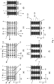
- Figure 1 depicts in sub figures a) to g) an example of the method according to the disclosure, the various steps being denoted with Figures 1a-1f .
- a metallic lead frame 1 which fabricated from a metal sheet is provided, the metallic lead frame 1 being suited for having multiple semiconductor die components mounted thereon.
- the metallic lead frame 1 can be chosen from any electrically conductive metal material but preferably copper is used for the lead frame.
- the lead frame 1 has a planar structure with a first longitudinal dimension x1 and a second longitudinal dimension x2.
- first longitudinal dimension x1 and the second longitudinal dimension x2 are oriented perpendicular to each other, in an orthogonal axis orientation.
- both longitudinal dimensions x1 and x2 can have a non-perpendicular orientation with respect to each other, with an acute angle being smaller than 90°.
- the lead frame 1 comprise a plurality die paddles 2, which are oriented in a die paddle column 3 extending in or parallel to the first longitudinal dimension x1.
- the lead frame 1 comprises three die paddle columns 3 which seen in the second longitudinal dimension x2 are oriented parallel to each other.
- the die paddle columns 3 are oriented in the first longitudinal dimension x1, which first orientation x1 also can be referred as vertically or a vertical orientation.
- the lead frame 1 has plurality of terminals 4 (4a-4b), in this example, each die paddle 2 has two terminals 4a-4b provided forming a terminal pair. Of each terminal pair, one terminal 4a of the pair is connected with the die paddle 2 and the other terminal 4b is separately mounted in the lead frame 1, being not connected with the respective die paddle 2.
- step a) the terminals 4a-4b of each die paddle 2 each form a terminal column 5a-5b oriented in the first longitudinal dimension x1 (vertically).
- Some parts of terminals 4a-4b and die paddles 2 have additional frame connections 15 with the lead frame 1 and to each other for providing a mechanical straight and stiffness during manufacturing the semiconductor package assemblies.
- This additional frame connections 15 are known in the prior art as construction strengthening elements and will be removed during the further steps of manufacturing.
- Step b) of the method according to the disclosure pertains attaching semiconductor die components 6 to each of the die paddles 2.
- Step c) of the method according to the disclosure pertains to electrically connecting the semiconductor die components 6 with the plurality of terminals 4a using an electric connection 20, such as a bond clip 20.
- the semiconductor die components 6 are connected to the terminal 4a, in particular to the terminals 4a that are separated from the die paddles 2.
- one electric connection (bond clip) 20 is made but there are other configurations of connection possible including connecting each semiconductor die component 6 to more than one terminals 4a-4b.
- step d) of the method according to the disclosure pertains to encapsulating the plurality of semiconductor die components 6 by covering pairs of the one die paddle column 3 and the one terminal column 4a and/or 4b with a dielectric material 8. According to this method whole terminal columns 4a and/or 4b are being covered with dielectric material 8, but parts of the terminals 4a-4b, which terminal parts are denoted with reference numeral 7, are at least partly exposed.
- the exposed parts 7 of terminals 4a-4b which are not covered with the dielectric material 8 allow the semiconductor package 9 to be - during later applications - stable soldered to a printed circuit board (PCB), not shown.
- the dielectric material 8 forms a single encapsulation block with an elongated orientation parallel to the first longitudinal dimension x1.
- Each encapsulating block 8 consist of the at least one die paddle column 3 and the at least one terminal column 4a-4b, thus encapsulating multiple semiconductor die components 6. Note, that of each terminal column 4a-4b, the respective terminals 4a and 4b have exposed terminal parts 7 extending from the encapsulating block / dielectric material 8.
- the several encapsulating blocks 8 are separated from each other in the second longitudinal dimension x2 by means of a spacing S2, this separation is needed for trimming the lead frame 1.
- the next step is shown in Figure 1f and comprises trimming the exposed terminal parts 7 by removing the connections 15.
- a semiconductor package terminal 7 is formed, which - during later handling applications - is suitable for mounting to an electronic circuit e.g. through soldering.
- the exposed semiconductor package terminals 7 may be further undergo a shaping step after the trimming step ( Figure 1f ) in order to obtain a standardized dimension, which might be different per semiconductor package type. In this step some or all additional connections 15 are trimmed and/or removed.
- the several semiconductor packages 9 in each encapsulating blocks 8 are singulated by cutting each single encapsulation block 8 several times in the second longitudinal direction x2.
- the pathway of the cutting tool is denoted as the cutting line 10, which is parallel to the second longitudinal direction x2, and which pathway or cutting line 10 lays at least between the at least two semiconductor die components 6 of each die paddle column 3.
- the cutting process is to be performed between the die paddles 2, but the cutting process may also be performed through the die paddles 2.
- trimming step of Figure 1f and the singulating step of Figure 1g can be interchanged in the manufacturing sequence, meaning that in the alternative sequence the singulating step in Figure 1g is performed directly after performing the step d) of Figure 1d , and that the singulating step of Figure 1g is followed by the trimming step of Figure 1f .
- the spacing S1 between the singulated, encapsulated semiconductor packages assemblies is much more reduced (is much smaller) compared the spacing in other know methods.
- the spacing S1 between the singulated, encapsulated semiconductor packages 9 is only limited by the width 10 of cutting tool or cutting process requirements.
- the spacing is not limited by the method itself or by the material used for the encapsulating process, and therefore the spacing S1 can become significantly smaller as the width of the cutting tools used can be up to 0.03 mm thin.
- the semiconductor die components 6 are attached to the die paddles 2 by means of solder bonding using a soldering material.
- the semiconductor die component 6 can be attached to the die paddle 2 by means of adhesive bonding e.g. glue or eutectic bonding.
- the method according to the disclosure also includes surface treatment steps.
- Surface treatments changes the properties of the surface parts of the several elements making them more or less susceptible to chemicals and atmospheres thus making them more or less adhesive e.g. through brushing, galvanizing, or etching, or making the surfaces more or less suitable for soldering e.g. through plating.
- Some surface treatments e.g. coating cause elements of the semiconductor package to be more resistant to atmospheric conditions.
- Such surface treatments may be performed on any of the steps of the method according to the disclosure, to all elements or to some elements e.g. only applied to the terminals 4a-4b.
- trimming step of Figure 1f is preceded with a plating step, wherein the exposed terminal parts 7 are plated with a material suitable for solder mounting a semiconductor package e.g. tin and tin alloys, gold, silver and silver alloys and others.
- a material suitable for solder mounting a semiconductor package e.g. tin and tin alloys, gold, silver and silver alloys and others.
- the spaces S1 between the singulated, encapsulated semiconductor packages 9 are limited by the width 10 of the cutting tool being implemented. Therefore it is possible to have two single semiconductor packages 9 to be separated by less than 3 mm, preferably by less than 1 mm seen in the second longitudinal direction x2. Preferably they are separated by a range of 0.03-0.35 mm, in particular by a range of 0.12-0.18 mm.
- single or individual semiconductor packages 9 are separated by a spacing S1 of 0.15 mm which can the width of a saw blade 10 used for singulation step of Figure 1f .
- this width S1 may be up to 0.03 mm, when a laser beam is used in the singulating step of Figure 1f as the cutting tool or cutting technique.
- Preferred cutting techniques are indeed laser cutting or mechanic sawing, preferably rotating blade sawing. However any technique suitable for cutting the encapsulation dielectric material 8 can be implemented.
- the dielectric material 8 is preferably an electrically insulating material suitable for protecting the semiconductor die components 6 from short circuits and from atmospheric exposure.
- Such materials 8 are well known in the state of the art and suitable materials may be selected from polymers resins for casting.
- the resin 8 may be a photo-, a chemo-, or a thermo-curable resin when the encapsulation step is performed by mold casting.
- the encapsulation step is performed using injection molding of a thermoplastic polymer e.g. Polypropylene, Polyamide, Polyacetal, Polycarbonate, Poly(methyl methacrylate) and such.
- Other dielectric materials 8 used may be ceramic materials or ceramic composite materials.
- the singulated semiconductor package 9 as manufactured using the method according to the disclosure comprises at least one side wall 13 which is orientated parallel to the second longitudinal dimension x2.
- the side wall 13 has substantially flat surface which is perpendicular to a bottom side 11 or a top side 12 of the semiconductor package 9.
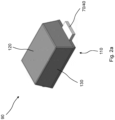
- the state of the art package 90 of Figure 2a is shown with exposed terminal parts 70 of the terminals 40 and with side walls 130 which are angled with respect to the bottom side 110 and/or the top side 120.
- a single semiconductor package 9 according to the disclosure is shown having two terminals 4a-4b on one side and one terminal 4c on the opposite side. It has side walls 13 with a substantially flat surface which surface is perpendicular to the bottom side 11 and/or the top side 12 of the semiconductor package 9.
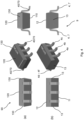
- Figure 3a shows a state of the art semiconductor package 90 with exposed terminal parts 70 of the terminals 40 and with angled side walls 130 which are angled with respect to the bottom side 110 and/or the top side 120, similar as in the state of the art example of Figure 2a .
- FIG 4b a standard SOT23 package 9 manufactured according the disclosure is shown.
- the side wall 13 has a flat orientation and is oriented perpendicular to both the bottom side 11 and the top side 12 of the semiconductor package 9, contrary to the state of the art package 90 as shown in Figure 4a with exposed terminal parts 70 of the terminals 40 and with angled side walls 130 which are angled with respect to the bottom side 110 and/or the top side 120, similar as the state of the art example of Figure 2a .
- the semiconductor package 9 has three terminals 4a-4c on each side of the package (six terminals 4a-4f in total), of which the exposed terminal parts 7 are cut and bended to a standardized shape in the step e) of the method according to the disclosure.
- FIG. 5b another embodiment is shown, showing a SOT363 package according to the disclosure, also having three terminals 4a-4c on each side of the package (six terminals 4a-4f in total).
- the side walls 13 have a flat surface and are oriented perpendicular to both the bottom side 11 and the top side 12 of the semiconductor package / SOT363.
- the exposed terminal parts 7 were cut and bended to a standardized shape in the step e) of the method.
- the state of the art package 90 as shown in Figure 5a has angled side walls 130 which are angled with respect to the bottom side 110 and/or the top side 120, similar as the state of the art example of Figure 2a .
Landscapes
- Encapsulation Of And Coatings For Semiconductor Or Solid State Devices (AREA)
- Lead Frames For Integrated Circuits (AREA)
Abstract
The present disclosure relates to manufacturing techniques for manufacturing multiple semiconductor package assemblies on a lead frame as well as a semiconductor package assembly manufactured using this method. The method aims to reduce the distances or intermediate spacings between singulated semiconductor packages on a lead frame to a width equal to the width of a cutting tool which width is significantly smaller than the distance required in any known modelling encapsulation technique. Therefore the method according to the disclosure allows to position more semiconductor packages on a lead frame on one process step. Accordingly, as the number of semiconductor packages per lead frame surface is increased, more semiconductor packages can manufactured and singulated in one process step, which reduces costs and processing time.
Description
- The present disclosure relates to manufacturing techniques for manufacturing multiple semiconductor package assemblies on a lead frame as well as a semiconductor package assembly manufactured using this method.
- When manufacturing a semiconductor package assembly, semiconductor components forming the semiconductor package are mounted to a lead frame and one or more bond clips are electronically connected with either the semiconductor die or with the lead frame. For finalizing the semiconductor package assembly, the semiconductor package is encapsulated using a dielectric material like plastic resin, thus immobilizing and protecting the fragile solder connection between the bond clips and the semiconductor die and the lead frame and allowing a proper handling and processing of the semiconductor package assembly in semiconductor applications.
- The encapsulation step requires that a space is left between each semiconductor package assembly, which space big enough to fit a mould cavity wall. Mould cavity walls must be strong enough to hold the dielectric material processing pressure that is required in the encaustic process using proper techniques. The most common encapsulation technique is injection moulding of a thermoplastic polymer. This process requires high pressures and temperature so the cavity walls are thick. Therefore the multiple semiconductor package assemblies must be spread out significantly across the lead frame surface. This reduces the possible number of semiconductor package assemblies encapsulated in one encapsulation process per lead frame as the dimensions of the encapsulation mould (of any kind) is limited.
- Accordingly, it is a goal of the present disclosure to provide an improved method of manufacturing semiconductor package assemblies as well as a semiconductor package assembly manufactured using this method, in which the spaces between the individual semiconductor package assemblies on one lead frame are significantly reduced.
- In a particular example of the method according to the disclosure, the method comprises the steps: a) providing a metallic lead frame fabricated from a metal sheet having a first longitudinal dimension and a second longitudinal dimension, the lead frame composed of a plurality of die paddles forming at least one die paddle column oriented in the first longitudinal dimension and a plurality of terminals forming at least one terminal column oriented in the first longitudinal dimension. In a further step b) a plurality of semiconductor die components are attached to each of the plurality of die paddles. In a next step c) a connection between the semiconductor die components with the plurality of terminals is performed. Step c) is followed by step d) which comprises step of encapsulating the plurality of semiconductor die components by covering at least one pair of the at least one die paddle column and the at least one terminal column with the terminal parts at least partly exposed with a dielectric material.
- Thus step d) thereby forms a single encapsulation block for each pair consisting of the at least one die paddle column and the at least one terminal column. In a next step e) trimming the exposed terminal parts is performed, followed by step f) of singulating semiconductor packages by cutting the at least one single encapsulation block in the second longitudinal direction into at least two single semiconductor packages. When performing the singulating step f) the cutting line lays at least between the at least two semiconductor die components. Alternatively, it is noted that steps e) and f) can be interchanged in the manufacturing sequence, meaning that in the alternative sequence the singulating step f) is performed directly after performing step d), and that step f) is followed by the trimming step e).
- The resulting method as outlined above reduces the distances or intermediate spacings between the singulated semiconductor packages on the lead frame to a width equal to the width of a cutting tool using for step f) which width is significantly smaller than the distance required in any known modelling encapsulation technique. Therefore the method according to the disclosure allows to position more semiconductor packages on a lead frame on one process step. Accordingly, as the number of semiconductor packages per lead frame surface is increased, more semiconductor packages can manufactured and singulated in one process step, which reduces costs and processing time.
- In particular, with the method according to the disclosure, lead frames can be processed with a higher density of semiconductor packages which will result in an increased throughput.
- In a detail of the method according to the disclosure, the step b) further may comprise the step of attaching the semiconductor die components to the die paddles by means of adhesive bonding, eutectic bonding or solder bonding. Due to the higher number of semiconductor packages per lead frame surface area, bonding distances can be shortened, increasing the indexing speed.
- In a further example of the disclosure any one of the steps a) to f) are preceded by a surface treatment step, a coating step, a plating step or a galvanizing step.
- In a preferred example, step e) is preceded with a step g) of plating the exposed terminal parts with a material suitable for solder mounting a semiconductor package.
- In yet another example, the step g) of plating the exposed terminal parts comprises plating with a tin alloy suitable for solder mounting a semiconductor package.
- In another beneficial example according to the disclosure the manufacturing method allows for at least two single semiconductor packages being separated by a distance or spacing of less than 3 mm, preferably less than 1 mm seen in second longitudinal direction. Preferably, the spacing between the at least two single semiconductor packages exhibits a range of 0.03-0.35 mm, in particular a range of 0.12-0.18 mm, in particular the spacing is 0.15 mm.
- Next, another beneficial example according to the disclosure relates to the step d) being performed using injection moulding of a thermoplastic polymer. Alternatively, the step d) may be performed using polymer resin casting, wherein the resin is a photo-, a chemo-, or a thermo-curable resin. In another example according to the disclosure the step d) may be performed using a ceramic material.
- For singulating the individual semiconductor packages the step f) may comprise the technique of laser cutting or mechanic sawing.
- The disclosure also pertains to a semiconductor package manufactured using the disclosed method, with at least one side wall of the semiconductor package being orientated parallel to the second longitudinal dimension of the metallic lead frame having substantially a flat surface which flat surface is positioned perpendicular to a bottom side or a top side of the semiconductor package.
- The disclosure will now be discussed with reference to the drawings, which show in:
-
Figure 1a-1g the various steps of an example of a method according to the disclosure; -
Figure 2a an examples of a semiconductor package (assembly) according to the prior art; -
Figure 2b an example of a semiconductor package (assembly) according to the disclosure; -
Figure 3a-3b another example of a semiconductor package (assembly) according to the prior art and the disclosure; -
Figure 4a-4b another example of a semiconductor package (assembly) according to the prior art and the disclosure; -
Figure 5a-5b another example of a semiconductor package (assembly) according to the prior art and the disclosure; -
Figure 6 an example of a schematic lead frame design according to the disclosure. - For a proper understanding of the disclosure, in the detailed description below corresponding elements or parts of the disclosure will be denoted with identical reference numerals in the drawings.
-
Figure 1 depicts in sub figures a) to g) an example of the method according to the disclosure, the various steps being denoted withFigures 1a-1f . In a first step a) ametallic lead frame 1 which fabricated from a metal sheet is provided, themetallic lead frame 1 being suited for having multiple semiconductor die components mounted thereon. Themetallic lead frame 1 can be chosen from any electrically conductive metal material but preferably copper is used for the lead frame. Thelead frame 1 has a planar structure with a first longitudinal dimension x1 and a second longitudinal dimension x2. - In this particular example, the first longitudinal dimension x1 and the second longitudinal dimension x2 are oriented perpendicular to each other, in an orthogonal axis orientation. However, it can be envisaged that both longitudinal dimensions x1 and x2 can have a non-perpendicular orientation with respect to each other, with an acute angle being smaller than 90°.
- The
lead frame 1 comprise aplurality die paddles 2, which are oriented in adie paddle column 3 extending in or parallel to the first longitudinal dimension x1. In this particular example, thelead frame 1 comprises threedie paddle columns 3 which seen in the second longitudinal dimension x2 are oriented parallel to each other. Thedie paddle columns 3 are oriented in the first longitudinal dimension x1, which first orientation x1 also can be referred as vertically or a vertical orientation. - The
lead frame 1 has plurality of terminals 4 (4a-4b), in this example, eachdie paddle 2 has twoterminals 4a-4b provided forming a terminal pair. Of each terminal pair, oneterminal 4a of the pair is connected with thedie paddle 2 and theother terminal 4b is separately mounted in thelead frame 1, being not connected with therespective die paddle 2. - Furthermore, in step a) the
terminals 4a-4b of eachdie paddle 2 each form aterminal column 5a-5b oriented in the first longitudinal dimension x1 (vertically). Some parts ofterminals 4a-4b anddie paddles 2 haveadditional frame connections 15 with thelead frame 1 and to each other for providing a mechanical straight and stiffness during manufacturing the semiconductor package assemblies. Thisadditional frame connections 15 are known in the prior art as construction strengthening elements and will be removed during the further steps of manufacturing. - Step b) of the method according to the disclosure pertains attaching
semiconductor die components 6 to each of thedie paddles 2. - Step c) of the method according to the disclosure pertains to electrically connecting the
semiconductor die components 6 with the plurality ofterminals 4a using anelectric connection 20, such as abond clip 20. Thesemiconductor die components 6 are connected to theterminal 4a, in particular to theterminals 4a that are separated from thedie paddles 2. In this example one electric connection (bond clip) 20 is made but there are other configurations of connection possible including connecting each semiconductor diecomponent 6 to more than oneterminals 4a-4b. - Following step c), step d) of the method according to the disclosure pertains to encapsulating the plurality of semiconductor die
components 6 by covering pairs of the onedie paddle column 3 and the oneterminal column 4a and/or 4b with adielectric material 8. According to this method wholeterminal columns 4a and/or 4b are being covered withdielectric material 8, but parts of theterminals 4a-4b, which terminal parts are denoted withreference numeral 7, are at least partly exposed. - The exposed
parts 7 ofterminals 4a-4b which are not covered with thedielectric material 8 allow thesemiconductor package 9 to be - during later applications - stable soldered to a printed circuit board (PCB), not shown. After the encapsulating step d), thedielectric material 8 forms a single encapsulation block with an elongated orientation parallel to the first longitudinal dimension x1. Each encapsulatingblock 8 consist of the at least onedie paddle column 3 and the at least oneterminal column 4a-4b, thus encapsulating multiple semiconductor diecomponents 6. Note, that of eachterminal column 4a-4b, therespective terminals terminal parts 7 extending from the encapsulating block /dielectric material 8. - As shown in
Figure 1d , the several encapsulatingblocks 8 are separated from each other in the second longitudinal dimension x2 by means of a spacing S2, this separation is needed for trimming thelead frame 1. - The next step is shown in
Figure 1f and comprises trimming the exposedterminal parts 7 by removing theconnections 15. Herewith, asemiconductor package terminal 7 is formed, which - during later handling applications - is suitable for mounting to an electronic circuit e.g. through soldering. The exposedsemiconductor package terminals 7 may be further undergo a shaping step after the trimming step (Figure 1f ) in order to obtain a standardized dimension, which might be different per semiconductor package type. In this step some or alladditional connections 15 are trimmed and/or removed. - In the final step, as shown in
Figure 1g , of the method according to the disclosure theseveral semiconductor packages 9 in each encapsulating blocks 8 are singulated by cutting eachsingle encapsulation block 8 several times in the second longitudinal direction x2. The pathway of the cutting tool is denoted as the cuttingline 10, which is parallel to the second longitudinal direction x2, and which pathway or cuttingline 10 lays at least between the at least twosemiconductor die components 6 of each diepaddle column 3. The cutting process is to be performed between the die paddles 2, but the cutting process may also be performed through the die paddles 2. - Alternatively, it is noted that trimming step of
Figure 1f and the singulating step ofFigure 1g can be interchanged in the manufacturing sequence, meaning that in the alternative sequence the singulating step inFigure 1g is performed directly after performing the step d) ofFigure 1d , and that the singulating step ofFigure 1g is followed by the trimming step ofFigure 1f . - With the method according to the disclosure, the spacing S1 between the singulated, encapsulated semiconductor packages assemblies is much more reduced (is much smaller) compared the spacing in other know methods. The spacing S1 between the singulated, encapsulated
semiconductor packages 9 is only limited by thewidth 10 of cutting tool or cutting process requirements. The spacing is not limited by the method itself or by the material used for the encapsulating process, and therefore the spacing S1 can become significantly smaller as the width of the cutting tools used can be up to 0.03 mm thin. - In conformity with the method according to the disclosure in the step c) the
semiconductor die components 6 are attached to the die paddles 2 by means of solder bonding using a soldering material. In another example thesemiconductor die component 6 can be attached to thedie paddle 2 by means of adhesive bonding e.g. glue or eutectic bonding. - Furthermore the method according to the disclosure also includes surface treatment steps. Surface treatments changes the properties of the surface parts of the several elements making them more or less susceptible to chemicals and atmospheres thus making them more or less adhesive e.g. through brushing, galvanizing, or etching, or making the surfaces more or less suitable for soldering e.g. through plating. Some surface treatments e.g. coating cause elements of the semiconductor package to be more resistant to atmospheric conditions. Such surface treatments may be performed on any of the steps of the method according to the disclosure, to all elements or to some elements e.g. only applied to the
terminals 4a-4b. - In addition, as detailed in
Figure 1e , trimming step ofFigure 1f is preceded with a plating step, wherein the exposedterminal parts 7 are plated with a material suitable for solder mounting a semiconductor package e.g. tin and tin alloys, gold, silver and silver alloys and others. - According to the disclosure, the spaces S1 between the singulated, encapsulated
semiconductor packages 9 are limited by thewidth 10 of the cutting tool being implemented. Therefore it is possible to have twosingle semiconductor packages 9 to be separated by less than 3 mm, preferably by less than 1 mm seen in the second longitudinal direction x2. Preferably they are separated by a range of 0.03-0.35 mm, in particular by a range of 0.12-0.18 mm. - In the preferred embodiment as shown in
Figure 6 single orindividual semiconductor packages 9 are separated by a spacing S1 of 0.15 mm which can the width of asaw blade 10 used for singulation step ofFigure 1f . In other preferred embodiments this width S1 may be up to 0.03 mm, when a laser beam is used in the singulating step ofFigure 1f as the cutting tool or cutting technique. Preferred cutting techniques are indeed laser cutting or mechanic sawing, preferably rotating blade sawing. However any technique suitable for cutting theencapsulation dielectric material 8 can be implemented. - The
dielectric material 8 is preferably an electrically insulating material suitable for protecting thesemiconductor die components 6 from short circuits and from atmospheric exposure.Such materials 8 are well known in the state of the art and suitable materials may be selected from polymers resins for casting. Theresin 8 may be a photo-, a chemo-, or a thermo-curable resin when the encapsulation step is performed by mold casting. In other embodiments, the encapsulation step is performed using injection molding of a thermoplastic polymer e.g. Polypropylene, Polyamide, Polyacetal, Polycarbonate, Poly(methyl methacrylate) and such. Otherdielectric materials 8 used may be ceramic materials or ceramic composite materials. - Referring to
Figure 2b , thesingulated semiconductor package 9 as manufactured using the method according to the disclosure, comprises at least oneside wall 13 which is orientated parallel to the second longitudinal dimension x2. Theside wall 13 has substantially flat surface which is perpendicular to abottom side 11 or atop side 12 of thesemiconductor package 9. The state of theart package 90 ofFigure 2a is shown with exposed terminal parts 70 of the terminals 40 and withside walls 130 which are angled with respect to thebottom side 110 and/or thetop side 120. - In the example as shown in
Figure 3b , asingle semiconductor package 9 according to the disclosure is shown having twoterminals 4a-4b on one side and oneterminal 4c on the opposite side. It hasside walls 13 with a substantially flat surface which surface is perpendicular to thebottom side 11 and/or thetop side 12 of thesemiconductor package 9.Figure 3a shows a state of theart semiconductor package 90 with exposed terminal parts 70 of the terminals 40 and withangled side walls 130 which are angled with respect to thebottom side 110 and/or thetop side 120, similar as in the state of the art example ofFigure 2a . - In
Figure 4b , astandard SOT23 package 9 manufactured according the disclosure is shown. Theside wall 13 has a flat orientation and is oriented perpendicular to both thebottom side 11 and thetop side 12 of thesemiconductor package 9, contrary to the state of theart package 90 as shown inFigure 4a with exposed terminal parts 70 of the terminals 40 and withangled side walls 130 which are angled with respect to thebottom side 110 and/or thetop side 120, similar as the state of the art example ofFigure 2a . InFigure 4b , thesemiconductor package 9 has threeterminals 4a-4c on each side of the package (sixterminals 4a-4f in total), of which the exposedterminal parts 7 are cut and bended to a standardized shape in the step e) of the method according to the disclosure. - In
Figure 5b another embodiment is shown, showing a SOT363 package according to the disclosure, also having threeterminals 4a-4c on each side of the package (sixterminals 4a-4f in total). Likewise, theside walls 13 have a flat surface and are oriented perpendicular to both thebottom side 11 and thetop side 12 of the semiconductor package / SOT363. Similarly, the exposedterminal parts 7 were cut and bended to a standardized shape in the step e) of the method. The state of theart package 90 as shown inFigure 5a has angledside walls 130 which are angled with respect to thebottom side 110 and/or thetop side 120, similar as the state of the art example ofFigure 2a . -
- 1
- metallic lead frame
- x1
- first longitudinal dimension of
lead frame 1 - x2
- second longitudinal dimension of
lead frame 1 - 2
- die paddle
- 3
- die paddle column
- 4 (4a-4f)
- terminals
- 5a-5b
- terminal column
- 6
- semiconductor die component
- 7
- exposed terminal parts
- 8
- dielectric material / encapsulating block
- 9
- semiconductor package according to the disclosure
- 10
- cutting line / width of cutting tool (cutting blade / cutting saw / laser beam)
- 11
- bottom side
- 12
- topside
- 13
- side wall according to the disclosure
- 15
- frame connection
- 20
- electric connection / bond clip / bond wire
- S1
- spacing seen in first longitudinal direction x1
- S2
- spacing seen in second longitudinal direction x2
- 90
- semiconductor package according to the state of the art
- 40
- terminals of semiconductor package according to the state of the art
- 70
- exposed terminal parts of semiconductor package according to the state of the art
- 110
- bottom side of semiconductor package according to the state of the art
- 120
- top side of semiconductor package according to the state of the art
- 130
- side wall of semiconductor package according to the state of the art
Claims (12)
- A method of manufacturing a semiconductor package comprising the steps:a) providing a metallic lead frame (1) fabricated from a metal sheet having a first longitudinal dimension and a second longitudinal dimension the lead frame composed of a plurality of die paddles (2) forming at least one die paddle column (3) oriented in the first longitudinal dimension and a plurality of terminals (4) forming at least one terminal column (5) oriented in the first longitudinal dimension;b) attaching a plurality of semiconductor die component (6) to each of the plurality of die paddles (2);c) connecting the semiconductor die component (6) with the plurality of terminals;d) encapsulating the plurality of semiconductor die component (6) by covering at least one pair of the at least one die paddle column (3) and the at least one terminal column (4) with the terminal parts (7) at least partly exposed with dielectric material, thereby forming a single encapsulation block (8) for each pair consisting of the at least one die paddle column (3) and the at least one terminal column (4);e) trimming the exposed terminal parts (7);f) singulating semiconductor packages by cutting the at least one single encapsulation block in the second longitudinal direction into at least two single semiconductor packages (9) wherein the cutting line (10) lays at least between the at least two semiconductor die component (6).
- The method according to claim 1, wherein step c) comprises the step of attaching the semiconductor die component (6) to the die paddles (2) by means of adhesive bonding, eutectic bonding or solder bonding.
- The method according to claim 1 or 2, wherein any one of steps a) to f) is preceded with a surface treatment, a coating, a plating or a galvanizing step.
- The method according to any one or more of the claims 1 to 3, wherein step e) is preceded with the step g) of plating the exposed terminal parts(14) with a material suitable for solder mounting a semiconductor package.
- The method according to claim 4, wherein the step of plating the exposed terminal parts comprises plating with a tin alloy suitable for solder mounting a semiconductor package.
- The method according to any one or more of the claims 1 to 5, wherein at least two single semiconductor packages (9) are separated by less than 3 mm, preferably less than 1 mm seen in second longitudinal direction.
- The method according to claim 6, wherein at least two single semiconductor packages (9) are separated by a range of 0.03-0.35 mm, in particular by a range of 0.12-0.18 mm, in particular 0.15 mm.
- The method according to any one or more of the claims 1 to 7, wherein the step d is performed using injection molding of thermoplastic polymer.
- The method according to any one or more of the claims 1 to 8, wherein the step d is performed using polymer resin casting and the resin is a photo-, a chemo-, or a thermo-curable resin.
- The method according to any one or more of the claims 1 to 9, wherein the step d is performed using ceramic material.
- The method according to any one or more of the claims 1 to 10, wherein the step f is performed by means of laser cutting or mechanic sawing, preferably rotating blade sawing.
- A semiconductor package manufactured using the method according to any one or more of the method claims 1 to 11, wherein at least one side wall (13) of the semiconductor package orientated parallel to the second longitudinal dimension has substantially flat surface which is perpendicular to a bottom (11) or a top (12) side of the semiconductor package.
Priority Applications (3)
| Application Number | Priority Date | Filing Date | Title |
|---|---|---|---|
| EP22181793.5A EP4300552A1 (en) | 2022-06-29 | 2022-06-29 | A method of manufacturing semiconductor package assembly and a semiconductor package assembly manufactured using this method |
| CN202310781646.7A CN117612946A (en) | 2022-06-29 | 2023-06-29 | A method of manufacturing a semiconductor package component and a semiconductor package component manufactured using the method |
| US18/343,845 US20240006276A1 (en) | 2022-06-29 | 2023-06-29 | Method of manufacturing semiconductor package assembly and a semiconductor package assembly manufactured using this method |
Applications Claiming Priority (1)
| Application Number | Priority Date | Filing Date | Title |
|---|---|---|---|
| EP22181793.5A EP4300552A1 (en) | 2022-06-29 | 2022-06-29 | A method of manufacturing semiconductor package assembly and a semiconductor package assembly manufactured using this method |
Publications (1)
| Publication Number | Publication Date |
|---|---|
| EP4300552A1 true EP4300552A1 (en) | 2024-01-03 |
Family
ID=82608270
Family Applications (1)
| Application Number | Title | Priority Date | Filing Date |
|---|---|---|---|
| EP22181793.5A Withdrawn EP4300552A1 (en) | 2022-06-29 | 2022-06-29 | A method of manufacturing semiconductor package assembly and a semiconductor package assembly manufactured using this method |
Country Status (3)
| Country | Link |
|---|---|
| US (1) | US20240006276A1 (en) |
| EP (1) | EP4300552A1 (en) |
| CN (1) | CN117612946A (en) |
Citations (2)
| Publication number | Priority date | Publication date | Assignee | Title |
|---|---|---|---|---|
| US20110111562A1 (en) * | 2002-04-29 | 2011-05-12 | San Antonio Romarico S | Partially Patterned Lead Frames and Methods of Making and Using the Same in Semiconductor Packaging |
| US20210225744A1 (en) * | 2020-01-17 | 2021-07-22 | Infineon Technologies Ag | Leadframe, Encapsulated Package with Punched Lead and Sawn Side Flanks, and Corresponding Manufacturing Method |
Family Cites Families (3)
| Publication number | Priority date | Publication date | Assignee | Title |
|---|---|---|---|---|
| JP2011077458A (en) * | 2009-10-01 | 2011-04-14 | Panasonic Corp | Laser device |
| EP3736857A1 (en) * | 2019-05-07 | 2020-11-11 | Nexperia B.V. | Through hole side wettable flank |
| CN113035721A (en) * | 2019-12-24 | 2021-06-25 | 维谢综合半导体有限责任公司 | Packaging process for plating conductive film on side wall |
-
2022
- 2022-06-29 EP EP22181793.5A patent/EP4300552A1/en not_active Withdrawn
-
2023
- 2023-06-29 US US18/343,845 patent/US20240006276A1/en active Pending
- 2023-06-29 CN CN202310781646.7A patent/CN117612946A/en active Pending
Patent Citations (2)
| Publication number | Priority date | Publication date | Assignee | Title |
|---|---|---|---|---|
| US20110111562A1 (en) * | 2002-04-29 | 2011-05-12 | San Antonio Romarico S | Partially Patterned Lead Frames and Methods of Making and Using the Same in Semiconductor Packaging |
| US20210225744A1 (en) * | 2020-01-17 | 2021-07-22 | Infineon Technologies Ag | Leadframe, Encapsulated Package with Punched Lead and Sawn Side Flanks, and Corresponding Manufacturing Method |
Also Published As
| Publication number | Publication date |
|---|---|
| US20240006276A1 (en) | 2024-01-04 |
| CN117612946A (en) | 2024-02-27 |
Similar Documents
| Publication | Publication Date | Title |
|---|---|---|
| CN1155083C (en) | Electronic component and its manufacturing method and lead frame used therefor | |
| US6462273B1 (en) | Semiconductor card and method of fabrication | |
| US6467142B1 (en) | Method for manufacturing chip capacitor | |
| US11876003B2 (en) | Semiconductor package and packaging process for side-wall plating with a conductive film | |
| US11764075B2 (en) | Package assembly for plating with selective molding | |
| JP3209696B2 (en) | Electronic component manufacturing method | |
| KR20100115784A (en) | Flat leadless packages and stacked leadless package assemblies | |
| KR20010110154A (en) | Lead frame, semiconductor device and manufacturing the same, circuit substrate and electronic device | |
| US20240006276A1 (en) | Method of manufacturing semiconductor package assembly and a semiconductor package assembly manufactured using this method | |
| JPH07326797A (en) | Method for manufacturing a side-emitting semiconductor light-emitting device | |
| US20130285223A1 (en) | Method for manufacturing electronic devices | |
| US20230360928A1 (en) | Method for manufacturing semiconductor devices and corresponding semiconductor device | |
| US20240332141A1 (en) | Semiconductor device package for press fit assembly | |
| CN1697204A (en) | Light-emitting diode bracket and manufacturing method thereof | |
| US20180261469A1 (en) | Method for Making Lead Frames for Integrated Circuit Packages | |
| CN115910984A (en) | Semiconductor package and manufacturing method thereof | |
| US20250157829A1 (en) | Semiconductor device fabrication method and lead frame with side portion mold locking structure | |
| US20250140653A1 (en) | Hybrid quad flat package electronic device | |
| US20230411265A1 (en) | Split semiconductor package | |
| CN120511254A (en) | Semiconductor package | |
| EP4312250A1 (en) | Method of manufacturing semiconductor devices, corresponding substrate and semiconductor device | |
| US20250183129A1 (en) | Thermal enhanced electronic device package | |
| CN120072811A (en) | Semiconductor package | |
| CN112652583A (en) | Packaging device and production method thereof | |
| CN1445830A (en) | Discrete circuit element fabrication method |
Legal Events
| Date | Code | Title | Description |
|---|---|---|---|
| PUAI | Public reference made under article 153(3) epc to a published international application that has entered the european phase |
Free format text: ORIGINAL CODE: 0009012 |
|
| STAA | Information on the status of an ep patent application or granted ep patent |
Free format text: STATUS: THE APPLICATION HAS BEEN PUBLISHED |
|
| AK | Designated contracting states |
Kind code of ref document: A1 Designated state(s): AL AT BE BG CH CY CZ DE DK EE ES FI FR GB GR HR HU IE IS IT LI LT LU LV MC MK MT NL NO PL PT RO RS SE SI SK SM TR |
|
| STAA | Information on the status of an ep patent application or granted ep patent |
Free format text: STATUS: THE APPLICATION IS DEEMED TO BE WITHDRAWN |
|
| 18D | Application deemed to be withdrawn |
Effective date: 20240704 |