EP4297279A1 - Noise shaper variable quantizer - Google Patents
Noise shaper variable quantizer Download PDFInfo
- Publication number
- EP4297279A1 EP4297279A1 EP23175324.5A EP23175324A EP4297279A1 EP 4297279 A1 EP4297279 A1 EP 4297279A1 EP 23175324 A EP23175324 A EP 23175324A EP 4297279 A1 EP4297279 A1 EP 4297279A1
- Authority
- EP
- European Patent Office
- Prior art keywords
- quantizer
- signal
- scaling factor
- noise shaping
- nsh
- Prior art date
- Legal status (The legal status is an assumption and is not a legal conclusion. Google has not performed a legal analysis and makes no representation as to the accuracy of the status listed.)
- Pending
Links
Images






Classifications
-
- H—ELECTRICITY
- H03—ELECTRONIC CIRCUITRY
- H03M—CODING; DECODING; CODE CONVERSION IN GENERAL
- H03M1/00—Analogue/digital conversion; Digital/analogue conversion
- H03M1/06—Continuously compensating for, or preventing, undesired influence of physical parameters
- H03M1/08—Continuously compensating for, or preventing, undesired influence of physical parameters of noise
- H03M1/0854—Continuously compensating for, or preventing, undesired influence of physical parameters of noise of quantisation noise
-
- H—ELECTRICITY
- H03—ELECTRONIC CIRCUITRY
- H03M—CODING; DECODING; CODE CONVERSION IN GENERAL
- H03M1/00—Analogue/digital conversion; Digital/analogue conversion
- H03M1/06—Continuously compensating for, or preventing, undesired influence of physical parameters
- H03M1/0617—Continuously compensating for, or preventing, undesired influence of physical parameters characterised by the use of methods or means not specific to a particular type of detrimental influence
- H03M1/0634—Continuously compensating for, or preventing, undesired influence of physical parameters characterised by the use of methods or means not specific to a particular type of detrimental influence by averaging out the errors, e.g. using sliding scale
- H03M1/0656—Continuously compensating for, or preventing, undesired influence of physical parameters characterised by the use of methods or means not specific to a particular type of detrimental influence by averaging out the errors, e.g. using sliding scale in the time domain, e.g. using intended jitter as a dither signal
- H03M1/066—Continuously compensating for, or preventing, undesired influence of physical parameters characterised by the use of methods or means not specific to a particular type of detrimental influence by averaging out the errors, e.g. using sliding scale in the time domain, e.g. using intended jitter as a dither signal by continuously permuting the elements used, i.e. dynamic element matching
- H03M1/0665—Continuously compensating for, or preventing, undesired influence of physical parameters characterised by the use of methods or means not specific to a particular type of detrimental influence by averaging out the errors, e.g. using sliding scale in the time domain, e.g. using intended jitter as a dither signal by continuously permuting the elements used, i.e. dynamic element matching using data dependent selection of the elements, e.g. data weighted averaging
- H03M1/0668—Continuously compensating for, or preventing, undesired influence of physical parameters characterised by the use of methods or means not specific to a particular type of detrimental influence by averaging out the errors, e.g. using sliding scale in the time domain, e.g. using intended jitter as a dither signal by continuously permuting the elements used, i.e. dynamic element matching using data dependent selection of the elements, e.g. data weighted averaging the selection being based on the output of noise shaping circuits for each element
-
- H—ELECTRICITY
- H03—ELECTRONIC CIRCUITRY
- H03M—CODING; DECODING; CODE CONVERSION IN GENERAL
- H03M3/00—Conversion of analogue values to or from differential modulation
- H03M3/30—Delta-sigma modulation
- H03M3/458—Analogue/digital converters using delta-sigma modulation as an intermediate step
- H03M3/478—Means for controlling the correspondence between the range of the input signal and the range of signals the converter can handle; Means for out-of-range indication
- H03M3/488—Means for controlling the correspondence between the range of the input signal and the range of signals the converter can handle; Means for out-of-range indication using automatic control
- H03M3/492—Means for controlling the correspondence between the range of the input signal and the range of signals the converter can handle; Means for out-of-range indication using automatic control in feed forward mode, i.e. by determining the range to be selected directly from the input signal
-
- H—ELECTRICITY
- H03—ELECTRONIC CIRCUITRY
- H03M—CODING; DECODING; CODE CONVERSION IN GENERAL
- H03M1/00—Analogue/digital conversion; Digital/analogue conversion
- H03M1/06—Continuously compensating for, or preventing, undesired influence of physical parameters
- H03M1/0617—Continuously compensating for, or preventing, undesired influence of physical parameters characterised by the use of methods or means not specific to a particular type of detrimental influence
- H03M1/0626—Continuously compensating for, or preventing, undesired influence of physical parameters characterised by the use of methods or means not specific to a particular type of detrimental influence by filtering
-
- H—ELECTRICITY
- H03—ELECTRONIC CIRCUITRY
- H03M—CODING; DECODING; CODE CONVERSION IN GENERAL
- H03M1/00—Analogue/digital conversion; Digital/analogue conversion
- H03M1/06—Continuously compensating for, or preventing, undesired influence of physical parameters
- H03M1/0617—Continuously compensating for, or preventing, undesired influence of physical parameters characterised by the use of methods or means not specific to a particular type of detrimental influence
- H03M1/0634—Continuously compensating for, or preventing, undesired influence of physical parameters characterised by the use of methods or means not specific to a particular type of detrimental influence by averaging out the errors, e.g. using sliding scale
- H03M1/0643—Continuously compensating for, or preventing, undesired influence of physical parameters characterised by the use of methods or means not specific to a particular type of detrimental influence by averaging out the errors, e.g. using sliding scale in the spatial domain
- H03M1/0648—Continuously compensating for, or preventing, undesired influence of physical parameters characterised by the use of methods or means not specific to a particular type of detrimental influence by averaging out the errors, e.g. using sliding scale in the spatial domain by arranging the quantisation value generators in a non-sequential pattern layout, e.g. symmetrical
-
- H—ELECTRICITY
- H03—ELECTRONIC CIRCUITRY
- H03M—CODING; DECODING; CODE CONVERSION IN GENERAL
- H03M3/00—Conversion of analogue values to or from differential modulation
- H03M3/30—Delta-sigma modulation
- H03M3/50—Digital/analogue converters using delta-sigma modulation as an intermediate step
- H03M3/51—Automatic control for modifying converter range
Definitions
- This disclosure is related to the field of signal processing, and, more particularly, to a signal processing circuit utilizing variable scaling during re-quantization to reduce quantization noise and increase dynamic range without causing a transient audible phenomena referred to in the art as a "pop".
- the signal processing chain 1 includes a transmitter section (e.g., a noise shaping quantizer) 2 and a receiver section 15 (e.g., a digital to analog converter, DAC).
- a transmitter section e.g., a noise shaping quantizer
- a receiver section 15 e.g., a digital to analog converter, DAC
- the noise shaping quantizer 2 includes a noise shaping filter 3 that receives a noise shaping input signal nsh in .
- the noise shaping filter 3 performs filtering and utilizes error feedback to produce a quantizer input signal quantizer input .
- a quantizer 4 receives the quantizer input signal quantizer input and performs re-quantization to produce a noise shaping output signal nsh out .
- the receiver 15 may apply a single fixed factor ⁇ to the noise shaping output signal nsh out .
- the quantizer 4 includes a summer 5 through which a dither signal dither_in is injected to the quantizer input signal quantizer input prior to division by a fixed factor ⁇ in a divider 6.
- a truncation circuit 7 operates on the output of the divider 6, resulting in data loss, for example by rounding, saturation, or introducing of other non-linearities, producing the noise shaping output signal nsh out .
- a feedback multiplier 8 multiplies the noise shaping output signal nsh out by the same fixed factor ⁇ to produce a quantizer output signal quantizer output provided to the noise shaping filter 3.
- the fixed factor ⁇ is set to a minimum sufficient value for expected values of the noise shaping input signal nsh in . This means, however, that at certain values of the noise shaping input signal nsh in , the factor ⁇ is higher than strictly necessary, with the result being that dynamic range is lower than it could be.
- FIG. 2 showing a second prior art signal processing chain 1' (full details of which may be found in United States Patent No. 7,239,258 , incorporated by reference in its entirety).
- the quantization noise in the audio signal within the audio playback circuit 1' is the residual low power and high frequency signal resulting from re-quantization which occurs in the noise shaping circuit 4.
- the noise shaping input signal nsh is lower than a given threshold, it is possible to scale the noise shaping input signal nsh in by an adjustable factor ⁇ prior to noise shaping by the noise shaper 4, while maintaining the quantization performed at a fixed scaling factor 1 ⁇ , to lower the quantization noise and increase dynamic range.
- This scaling is performed by a multiplication circuit 21 that scales an input audio signal by the adjustable factor ⁇ to produce the noise shaping input signal nsh in .
- a dynamic range optimization (DYRO) control circuit 14 controls the adjustable factor ⁇ on the fly in an attempt to maximize the dynamic range and compensates the receiver 15 accordingly by an adjustable factor ⁇ (e.g., an adjustable scaling factor).
- DYRO dynamic range optimization
- the multiplication which results from the error feedback arrangement within the noise shaper 4' causes the injection of a transient disturbance in the feedback, and this transient disturbance is propagated through to the output signal where it manifests as a transient audible phenomena referred to in the art as a "pop".
- transient disturbance in the output from the noise shaping circuit 4 (labelled as o_nsh), transient disturbance in the signal in the noise shaping circuit 4 after re-quantization but prior to filtering (labelled as o_prefilt), and transient disturbance in the output of a filter within the noise shaping circuit 4 (labelled as o_filt), as shown for example by the output of an ITU filter labelled as itu), can be observed.
- this pop is undesirable, as the pop may be audible by the human ear.
- a signal processing circuit including a transmitter section.
- the transmitter section includes a noise shaper receiving a noise shaping input signal and a quantizer output signal, the noise shaper configured to generate a quantizer input signal based upon the noise shaping input signal and the quantizer output signal, and a quantizer receiving the quantizer input signal and configured to divide the quantizer input signal by a scaling factor to produce a noise shaping output signal and to multiply the noise shaping output signal by the scaling factor to product the quantizer output signal.
- the signal processing circuit also includes a receiver section, the receiver section including receiver circuitry receiving the noise shaping output signal, the receiver circuitry configured to scale the quantizer output signal by a second scaling factor, and a dynamic range optimization circuit.
- the dynamic range optimization circuit is configured to determine whether an absolute value of the noise shaping input signal is less than a threshold value, lower the scaling factor in response to the absolute value of the noise shaping input signal being less than the threshold value, and decrease the second scaling factor in response to the absolute value of the noise shaping input signal being less than the threshold value, proportionally to the lowering of the scaling factor such that a ratio between the scaling factor and the second scaling factor remains substantially constant.
- the dynamic range optimization circuit is further configured to increase the scaling factor in response to the absolute value of the noise shaping input signal being greater than the threshold value and increase the second scaling factor in response to the absolute value of the noise shaping input signalbeing greater than the threshold value, proportionally to the increase in the scaling factor such that the ratio between the scaling factor and second scaling factor remains substantially constant.
- a dither generator may be configured to generate a dither signal having a range defined by the scaling factor, and the transmitter section may include a summing circuit configured to inject the dither signal into the quantizer input signal prior to quantization thereof by the quantizer.
- the quantizer may apply a truncation to the quantizer input signal after division thereof by the scaling factor.
- the scaling factor may be a power of two.
- the quantizer input signal and quantizer output signal may be digital, and the quantizer may be implemented digitally.
- the quantizer input signal and quantizer output signal may be analog, and the quantizer may be implemented in an analog fashion, with the quantizer including an analog to digital converter (ADC) receiving the quantizer input signal and digitizing the quantizer input signal to produce the noise shaping output signal such that it is scaled by the scaling factor, and a digital to analog converter (DAC) receiving the noise shaping output signal and converting the noise shaping output signal to produce the quantizer output signal such that it is multiplied by the scaling factor.
- ADC analog to digital converter
- DAC digital to analog converter
- the receiver section may be implemented digitally.
- the receiver section may be implemented in an analog fashion.
- the noise shaper may include an input summer configured to subtract an error signal from the noise shaping input signal to produce the quantizer input signal, an error summer configured to subtract the quantizer input signal from the quantizer output signal to produce an intermediate output, and a noise shaping filter configured to apply a noise shaping filter function to the intermediate output to produce the error signal.
- the noise shaper may include a sigma delta modulator receiving the noise shaping input signal and the quantizer output signal as output and applying a two-input one-output filtering thereto to produce the quantizer input signal.
- the absolute value of the noise shaping signal may be determined from a current value of the noise shaping input signal.
- a signal processing method including generating a quantizer input signal based upon a noise shaping input signal and a quantizer output signal, dividing the quantizer input signal by a scaling factor to produce a noise shaping output signal, and multiplying the noise shaping output signal by the scaling factor to product the quantizer output signal.
- the method further includes scaling the quantizer output signal by a second scaling factor, determining whether an absolute value of the noise shaping input signal is less than a threshold value, lowering the scaling factor in response to the absolute value of the noise shaping input signal being less than the threshold value, and decreasing the second scaling factor in response to the absolute value of the noise shaping input signal being less than the threshold value, proportionally to the lowering of the scaling factor such that a ratio between the scaling factor and the second scaling factor remains substantially constant.
- the method may further include generating an analog output signal from at least the noise shaping output signal by selectively connecting or disconnecting current sources and current sinks to differential outputs in response to the noise shaping output signal (the current sources and current sinks being scaled by the second scaling factor), amplifying the analog output signal, and driving a speaker with the analog output signal.
- Adjustment of the scaling factor and the second scaling factor proportionally to one another may serve to prevent transients resulting from scaling factor adjustment from being present in the noise shaping output signal and therefore from causing audible pops to be played by the speaker.
- the method may include increasing the scaling factor in response to the absolute value of the noise shaping input signal being greater than the threshold value and increasing the second scaling factor in response to the absolute value of the noise shaping input signalbeing greater than the threshold value, proportionally to the increase in the scaling factor such that the ratio between the scaling factor and second scaling factor remains substantially constant.
- the method may include generating a dither signal having a range defined by the scaling factor and injecting the dither signal into the quantizer input signal prior to quantization thereof.
- the method may include applying a truncation to the quantizer input signal after division thereof by the scaling factor.
- the scaling factor may be a power of two.
- a sample signal processing chain 20 including a transmitter section (e.g., a noise shaping quantizer) 21 and a receiver section 35 (e.g., a digital to analog converter, DAC).
- the transmitter section 21 may be analog or digital
- the receiver section 35 may be analog or digital.
- the noise shaping quantizer 21 includes a noise shaping filter 23 that receives a noise shaping input signal nsh in .
- the noise shaping filter 23 performs filtering and utilizes error feedback to produce a quantizer input signal quantizer input .
- a quantizer 24 receives the quantizer input signal quantizer input and, under control of a dynamic range optimization circuit (DYRO control circuit) 34 as will be explained below, performs noise shaping and on-the-fly scaling on the noise shaping input signal nsh in to produce a noise shaped output signal nsh out .
- DYRO control circuit dynamic range optimization circuit
- the quantizer input signal quantizer input is divided by an adjustable factor ⁇ (e.g., a scaling factor) in a divider 26.
- a truncation circuit 27 operates on the output of the divider 26, resulting in data loss, for example by rounding, saturation, or introducing of other non-linearities, producing the noise shaping output signal nsh out .
- a feedback multiplier 28 multiplies the noise shaping output signal nsh out by the same adjustable factor ⁇ to produce a quantizer output signal quantizer output provided to the noise shaping filter 23 for use in performing noise shaping.
- the receiver section 35 multiplies the noise shaping output signal nsh out by another adjustable factor ⁇ (e.g., a scaling factor) to produce an output signal OUT.
- the adjustablefactor ⁇ and adjustable factor ⁇ may also be referred to as scaling factors herein.
- the different potential valuables of the adjustable factors ⁇ and ⁇ may be represented by an index k, for example, ⁇ k and ⁇ k .
- the DYRO control circuit 34 monitors the noise shaping input signal nsh in and based upon the amplitude thereof, adjusts the adjustable factor ⁇ and the adjustable factor ⁇ on the fly so as to balance output signal OUT swing with its quantization noise, as will be described below, with such adjusting maintaining the ratio ⁇ ⁇ as being a fixed constant.
- the DYRO control circuit 34 compares the noise shaping input signal nsh in to a series of accurately defined thresholds, and sets the adjustable factor ⁇ and the adjustable factor ⁇ on the fly based upon those comparisons.
- ⁇ and ⁇ may each take one of i different values.
- nsh in ⁇ i ⁇ nsh out the following relationship is present: nsh in ⁇ i ⁇ nsh out .
- nsh out max (which is set by limits inherent to the implementation of the quantizer 24)
- nsh in max i ⁇ nsh out max ⁇ ⁇ i .
- nsh in max ( i ) is therefore the maximum of the absolute value of the noise shaping input nsh in at the value of ⁇ i .
- ⁇ i [ ⁇ 1 ; ⁇ 2 ; ⁇ 3 ], with ⁇ 1 > ⁇ 2 > ⁇ 3
- a i [ ⁇ 1 ; ⁇ 2 ; ⁇ 3 ], with ⁇ 1 > ⁇ 2 > ⁇ 3
- TH i [ TH 1 , TH 2 , and TH 3 ] with TH 1 > TH 2 > TH 3 .
- the greater the adjustable factors ⁇ and ⁇ the greater the output signal OUT swing but also the greater the quantization noise.
- the lesser the adjustable factors ⁇ and ⁇ the lesser the output signal OUT swing and the lesser the quantization noise.
- the DYRO control circuit 34 may implement a margin in its thresholds and therefore in its threshold comparisons.
- the margin value is greater than zero but less than one.
- Time filtering may be performed on the threshold comparisons by the DYRO control circuit 34 in the falling direction.
- the DYRO control circuit 34 may wait to take action to change the adjustable factor ⁇ and the adjustable factor ⁇ until after the noise shaping input signal nsh in has fallen below and remained below the threshold in question (e.g., has fallen below TH 1 ) for a given period of time.
- Such time filtering may optionally be performed in the rising direction (such as when the noise shaping input signal nsh in was previously less than TH 1 and greater than TH 2 , but is now greater than TH 1 ) as well, although this may not be desired in some situations.
- the dither signal dither_in is generated by a dither circuit 38 under control of the DYRO control circuit 34 according to changes made to the adjustable factor ⁇ . Dithering prevents correlation between the quantization noise and the desired information represented by the output signal OUT.
- the injected dither may have a triangular probability distribution function as shown in FIG. 6 , with the specific shape of the probability distribution function changing with ⁇ . Details of this type of dithering may be found in Digital Dither, S. P. Lipshitz and, J. Vanderkooy, In Audio Engineering Society Convention 81, Nov 1986 , the contents of which are incorporated by reference in their entirety.
- the injected dither may instead have a rectangular probability function, also in instances where the quantizer 24 is digital.
- the dither circuit 38 under control of the DYRO control circuit 34, may supply the dither signal dither_in as two random analog values.
- the dither signal dither_in is injected to the quantizer input quantizer input prior to operation thereon by the divider 26, but is not subtracted from the quantizer output quantizer output .
- the quantizer 24 may include a subtractor 24 that subtracts the dither signal dither_in from the quantizer output quantizer output .
- LFSRs linear feedback shift registers
- the dither signal may be generated through any suitable circuit, and may take any suitable form.
- the quantizer 24 may not include dither injection, and the quantizer input quantizer input may be directly fed to the divider 26.
- the transmitter section 21 is described generically, and such description of operation applies to either an analog or a digital transmitter section.
- the receiver section 35 is described generically, and such description of operation applies to either an analog or digital receiver section 35.
- a sample digital quantizer 24' is shown in FIG. 9 and has the structure and function of the digital quantizer 24 described above.
- the adjustable factor ⁇ is equal to 2 ⁇ , and therefore the divider 26 performs a division of the quantizer input quantizer input (after dither injection) 2 ⁇ , while the feedback multiplier 28 multiplies the noise shaping output nsh out by 2 ⁇ .
- the data loss function 27 may be a round, floor, or ceiling function, for example. Note that it is possible in a digital implementation of the quantizer 24' for the adjustable factor ⁇ to instead be implemented as a ratio of two integers or as a floating point value, depending upon hardware.
- a sample generic analog quantizer 24" is shown in FIG. 10 .
- the analog quantizer 24" includes a summer 25 through which an analog dither signal dither_in is injected into the analog quantizer input signal quantizer input prior to analog to digital conversion by an analog to digital converter (ADC) 26'.
- ADC analog to digital converter
- ADC 26' an effective division of the quantizer input signal quantizer input by the adjustable factor ⁇ is performed.
- the output of the ADC 26' is the noise shaping output nsh out .
- a digital to analog converter (DAC) 28' converts the noise shaping output nsh out back to analog form, and performs an effective multiplication of the noise shaping output nsh out by the adjustable factor ⁇ to produce an analog quantizer output signal quantizer output .
- DAC digital to analog converter
- FIG. 11 One potential implementation of the analog quantizer 24" which is intended for use with a digital receiver section 35 is shown in FIG. 11 .
- the ADC 26' is arranged to be used to generate k thresholds for use in analog to digital conversion.
- a resistor ladder is connected between a positive voltage + V ⁇ and a negative voltage - V ⁇ , with these voltages having equal and opposite magnitudes set as a function of the current value of the adjustable factor ⁇ .
- the voltage ladder is formed by m resistors (m being equal to 2k+1) connected in series between + V ⁇ and - V ⁇ , and generates k positive threshold voltages and k negative threshold voltages.
- threshold voltages VTH1, ..., VTHk and -VTH1, ..., -VTHk are generated at taps between the resistors of the voltage ladder.
- the resistor directly connected to + V ⁇ has a resistance of R T 2 , as does the resistor directly connected to - V ⁇ .
- the remainder of the resistors each have a resistance of R T .
- the ADC 26' in this analog quantizer 24" shown in FIG. 11 includes 2k comparators, here shown as comparators 41(1), ..., 41(2k), providing output to 2k flip flops, here shown as flip flops 42(1), ..., 42(2k).
- the flip flops 42(1), ..., 42(2k) provide their outputs as selection signals to 2k switch circuits, here shown as switch circuits 44(1), ..., 44(2k).
- the comparators 41(1), ..., 41(2k) each have a non-inverting input terminal coupled to receive the quantizer input signal quantizer input , which is an analog voltage V quantizer_in in this instance.
- the comparators 41(1), ..., 41(2k) have respective inverting input terminals connected to different ones of the threshold voltages VTH1, ..., VTHk and -VTH1, ..., -VTHk.
- comparator 41(1) has its inverting input terminal connected to the threshold voltage VTHk
- comparator 41(2) has its inverting input terminal connected to the threshold voltage VTH1
- comparator 41(3) has its inverting input terminal connected to the threshold voltage -VTH1
- comparator 41(2k) has its inverting input terminal connected to the threshold voltage -VTHk.
- the flip flop 42(1) has its input receiving the output of the comparator 41(1) and has its output connected to provide a selection signal to the switch circuit 44(1)
- the flip flop 42(2) has its input receiving the output of the comparator 41(2) and has its output connected to provide a selection signal to the switch circuit 44(2)
- flip flop 42(3) has its input receiving the output of the comparator 41(3) and has its output connected to provide a selection signal to the switch circuit 44(3)
- flip flop 42(2k) has its input receiving the output of the comparator 41(2k) and has its output connected to provide a selection signal to the switch circuit 44(2k).
- Each switch circuit 44(1), ..., 44(2k) operates to selectively connect an associated resistor (each such resistor having a resistance of R1) between either + V ⁇ or - V ⁇ and an inverting input terminal of an amplifier 45, under control of the output of a respective flip flop 42(1), ..., 42(2k).
- an associated resistor each such resistor having a resistance of R1
- the associated switch circuit 44(1), ..., 44(2k) connects its respective resistor to - V ⁇ and otherwise connects its respective resistor to V ⁇ .
- the amplifier 45 has its non-inverting input terminal grounded, and a resistor R2 is connected between the inverting input terminal and output of the amplifier 45.
- the output of the amplifier 45 is the quantizer output quantizer output , which is an analog voltage V quantizer _ out in this instance.
- R 1 m ⁇ 1 ⁇ R 2
- each flip flop 42(1), ..., 42(2k) is also connected to circuit 46 (illustratively a thermometric to signed converter 46 that generates the noise shaping output nsh out in digital form therefrom).
- the voltages + V ⁇ and - V ⁇ are based upon the adjustable factor ⁇ .
- the voltages + V ⁇ and - V ⁇ may be generated by a programmable voltage generator, with V ⁇ depending on the adjustable factor ⁇ (e.g., where the adjustable factor ⁇ changes from ⁇ 1 to ⁇ 2, V ⁇ changes from V y 1 to V y 2 ).
- the ADC 26' and DAC 28' may be integrated within a noise shaper utilizing either an error feedback or sigma-delta modulator arrangement.
- FIG. 12A A first potential implementation of the analog quantizer 24" which is intended for use with an analog receiver section 35 is shown in FIG. 12A .
- the converter 46' in this instance includes 2k switch circuits 47(1), ..., 47(2k) respectively connected to receive the outputs of flip flops 42(1), ..., 42(2k) as respective selection signals.
- the output of the flip flops 42(1), ..., 42(2k) here forms the noise shaping output nsh out .
- Each switch circuit 47(1), ..., 47(2k) operates to selectively connect an associated resistor (each such resistor having a resistance of R3) between either + V ⁇ or -V ⁇ and a non-inverting input terminal of an amplifier 48, under control of the output of a respective flip flop 42(1), ..., 42(2k).
- an associated resistor each such resistor having a resistance of R3
- the associated switch circuit 47(1), ..., 47(2k) connects its respective resistor to -V ⁇ and otherwise connects its respective resistor to V ⁇ .
- the voltages + V ⁇ and -V ⁇ are based upon the adjustable factor ⁇ .
- the voltages +V, and -V ⁇ may be generated by a programmable voltage generator, with V ⁇ depending on the adjustable factor ⁇ (e.g., where the adjustable factor ⁇ changes from ⁇ 1 to ⁇ 2, V ⁇ changes from V ⁇ 1 to V ⁇ 2 ).
- the amplifier 48 has its non-inverting input terminal grounded, and a resistor R4 is connected between the inverting input terminal and output of the amplifier 48.
- the output of the amplifier 48 may be used for desired purposes.
- R 3 m ⁇ 1 ⁇ R 4
- FIG. 12B A second potential implementation of the analog quantizer 24" is shown in FIG. 12B .
- the difference here is that the noise shaping output nsh out is produced at the output of the amplifier 48 as an analog voltage to be fed to the receiver 35', and here the receiver 35' is not scaled by the adjustable factor ⁇ because that scaling is performed by the converter 46'.
- a signal processing chain 100 is shown in FIG. 13 which includes a noise shaping digital quantizer as a digital transmitter section 22 and an analog receiver section 35.
- the noise shaping digital quantizer 22 operates as described above with reference to FIGS. 4, 5 , and 9 and needs no further description herein.
- the analog receiver section 35 includes a current steering DAC 150 that converts the noise shaping output signal nsh out to produce an analog output signal A out .
- the current steering DAC 150 includes a thermometric code conversion circuit that selects elementary contributions to the analog output signal A out that are scaled by the adjustable factor ⁇ .
- a low pass filter 151 filters quantization noise from the analog output signal A out , and the analog output signal A out is then amplified by a power amplifier 152 that drives a speaker 153 or other output device.
- the DAC 150 may be any suitable type of DAC, however, as an example, the illustrated DAC 150 is a current steering DAC that receives the noise shaping output signal nsh out as input.
- the current sources and current sinks each respectively source or sink a current Iref having a same magnitude multiplied by ⁇ . Stated differently, these currents are equal and each changed in magnitude proportionally to the current reference.
- the current sources are labeled in FIG. 14 as sourcing currents ⁇ ⁇ Iref 1 , ..., ⁇ ⁇ Iref N and the current sinks are labeled in FIG. 14 as sinking currents ⁇ ⁇ Iref 1 , ..., ⁇ ⁇ Iref N .
- a signal processing chain 100' is shown in FIG. 15 which includes a noise shaping digital quantizer 24' as a digital transmitter section 22 and a digital receiver section 35.
- the noise shaping digital quantizer 22 operates as described above with reference to FIGS. 4, 5 , and 9 and needs no further description herein.
- the digital receiver section 35 includes a scaling circuit 154 that scales the noise shaping output nsh out by ⁇ to produce a digital output signal D out .
- the digital output signal D out is thereafter passed through a decimating low-pass filter 155 and then a digital elaboration circuit 156.
- a signal processing chain 101 is shown in FIG. 16 which includes an analog quantizer 24" as an analog transmitter section 22 and a digital receiver section 35.
- the analog quantizer 24" operates as described above with reference to FIGS. 10 , 11 , 12 and needs no further description herein.
- the digital receiver section 35 includes a scaling circuit 154 that multiplies the noise shaping output nsh out by ⁇ (with ⁇ ⁇ 1 or ⁇ ⁇ 1) to produce a digital output signal D out .
- the digital output signal D out is thereafter passed through a decimating low-pass filter 155 and then a digital elaboration circuit 156.
- a signal processing chain 101' is shown in FIG. 17 which includes an analog quantizer 24" as an analog transmitter section 22 and an analog receiver section 35.
- the analog quantizer 24" operates as described above with reference to FIGS. 10 , 12 and needs no further description herein.
- the analog transmitter section 22 operates as described above with reference to FIG. 12 and needs no further description herein.
- the noise shaping filter 23 used in the above-described embodiments may utilize error feedback or sigma-delta modulation.
- the noise shaping filter 23 includes an input summer 23a that subtracts an error signal err output by a noise shaping filter 23c from the noise shaping input signal nsh in to produce the quantizer input quantizer input .
- the digital quantizer 24' injects the dither signal dither in to the quantizer input quantizer input and divides the quantizer input quantizer input by the adjustable factor ⁇ (which in this instance may be 1/2 ⁇ ), with that result being truncated such as by a rounding, floor, or ceiling function to produce the noise shaping output signal nsh out .
- the digital quantizer 24' multiplies the noise shaping output signal nsh out to produce the quantizer output quantizer output .
- An error summer 23b subtracts the quantizer input quantizer input from the quantizer output quantizer output and provides the result to the noise shaping filter 23c which has a transfer function of H(z).
- the noise shaping filter 23c produces the error signal err as output.
- the above-described error feedback arrangement may also be used with an analog quantizer 24", as shown in FIG. 19 , and operating as described above with reference to FIG. 18 .
- the noise shaping filter 23' in which the noise shaping filter is implemented as a sigma-delta modulator 23a', and designed to work with a digital quantizer 24'.
- the sigma-delta modulator 23a' includes a U-input ( L 0 ) that receives the noise shaping input nsh in and a V-input ( L 1 ) that receives the quantizer output quantizer output , and the output of the sigma-delta modulator 23a' is the quantizer input quantizer input .
- the quantizer input quantizer input may be produced as a digital signal for use with the digital quantizer 24' ( FIG. 20 ), ormay be produced as an analog signal for use with the analog quantizer 24" ( FIG. 21 ).
- Sample sigma-delta modulator designs such as may be used in the embodiment of FIG. 20 may be found in Understanding Delta-Sigma Delta Data Converters, Pavan, Shanthi; Schreir, Richard; Temes, Gabor C., IEEE Press Series on Microelectronic Systems, IEEE 2017 , the contents of which are incorporated by reference.
- the transmitter section 21 includes a digital quantizer 24' and error feedback based noise shaping circuit 23 as described above, and the receiver section includes a current steering DAC 150 as described above
- the DYRO control circuit 14 compares the values of the noise shaping input nsh in to a series of thresholds, and based thereupon, adjusts the adjustable factor ⁇ and the adjustable factor ⁇ on the fly, with such adjusting maintaining the ratio ⁇ ⁇ as being a fixed constant.
- the noise shaping filter 23c is a finite impulse response filter with coefficients fircoeff k .
- Example operation is now described with additional reference to FIG. 23 .
- the noise shaping input signal nsh in is 24 bit
- the noise shaping output signal nsh out is 7 bit.
- the current reference I ref used by the DAC 15 is 1 ⁇ A.
- the input audio signal i_audio (which is interpolated to produce the noise shaping input nsh out ) is playing audio and not muted.
- the input audio signal i_audio is muted, and the noise shaping at the output nsh out of the noise shaping circuit 23 can be observed between times T1 and T2.
- the quantization noise prior to filtering within the noise shaping circuit 23 can be observed between times T1 and T2 as o_prefilt, and after filtering can observed between times T1 and T2 as o_filt.
- the DYRO control circuit 14 adjusts the reference current I ref within the DAC 14 accordingly by properly scaling ⁇ (keeping in mind that ⁇ ⁇ remains as a fixed constant), which in this case yields a reduction in the reference current ⁇ ⁇ I ref from 1 ⁇ A to 1 ⁇ 2 ⁇ A.
- the reduction of the quantization noise prior to filtering within the noise shaping circuit 23 can be observed between times T2 and T3 as o_prefilt, and after filtering can observed between times T2 and T3 as o_filt.
- nsh in is below the second threshold (which is lower than the first threshold), and therefore ⁇ is reduced to 15 by the DYRO control circuit 14. Since the adjustable factor ⁇ is being reduced by one, the DYRO control circuit 14 adjusts the reference current ⁇ ⁇ I ref within the DAC 14 accordingly, which in this case is a reduction from 1 ⁇ 2 ⁇ A to 1 ⁇ 4 ⁇ A.
- the further reduction of the quantization noise prior to filtering within the noise shaping circuit 23 can be observed after time T3 as o_prefilt, and after filtering can observed after time T3 as o_filt.
- the dither is adjusted according to the adjustable factor ⁇ .
- the dither range may be from [-2 ⁇ , 2 ⁇ ], with a triangular probability distribution, and with ⁇ being changed as the adjustable factor ⁇ is changed.
- the audio sampling circuit 200 includes a microphone 201 receiving input sound waves and converting them to an analog audio signal, which is then preconditioned by a preconditioning amplifier 202 to produce an analog audio input signal A in .
- the preconditioning amplifier 202 may have a low-pass filtering behavior because the noise shaping input signal nsh in is within a limited bandwidth range.
- a noise shaping converter 203 here a sigma-delta based analog to digital converter controlled based upon the adjustable factor ⁇ , receives the analog audio input signal A in and digitizes the analog audio input signal A in to produce the noise shaping input signal nsh in , which is then compensated by a compensation circuit 204 according to the adjustable factor ⁇ , and in turn decimated by a decimation filter 205 to produce output that may be used for suitable purposes, for example by a digital elaboration unit for further processing, for example in a wave file writing system.
- the DYRO control circuit 206 operates as described above, comparing the analog input signal A in to the thresholds and adjusting the adjustable factors ⁇ and ⁇ accordingly.
Landscapes
- Engineering & Computer Science (AREA)
- Theoretical Computer Science (AREA)
- Compression, Expansion, Code Conversion, And Decoders (AREA)
- Analogue/Digital Conversion (AREA)
Abstract
Description
- This disclosure is related to the field of signal processing, and, more particularly, to a signal processing circuit utilizing variable scaling during re-quantization to reduce quantization noise and increase dynamic range without causing a transient audible phenomena referred to in the art as a "pop".
- The following background is provided with specific examples to show issues related to quantization, with it being understood that this disclosure itself is in no way limited to the types and contexts of the examples provided in this background.
- A first prior art
signal processing chain 1 is now described with reference toFIG. 1 . Thesignal processing chain 1 includes a transmitter section (e.g., a noise shaping quantizer) 2 and a receiver section 15 (e.g., a digital to analog converter, DAC). - The
noise shaping quantizer 2 includes anoise shaping filter 3 that receives a noise shaping input signal nshin. Thenoise shaping filter 3 performs filtering and utilizes error feedback to produce a quantizer input signal quantizerinput. Aquantizer 4 receives the quantizer input signal quantizerinput and performs re-quantization to produce a noise shaping output signal nshout. Thereceiver 15 may apply a single fixed factor α to the noise shaping output signal nshout. - The
quantizer 4 includes asummer 5 through which a dither signal dither_in is injected to the quantizer input signal quantizerinput prior to division by a fixed factor γ in a divider 6. Atruncation circuit 7 operates on the output of the divider 6, resulting in data loss, for example by rounding, saturation, or introducing of other non-linearities, producing the noise shaping output signal nshout. A feedback multiplier 8 multiplies the noise shaping output signal nshout by the same fixed factor γ to produce a quantizer output signal quantizeroutput provided to thenoise shaping filter 3. The fixed factor γ is set to a minimum sufficient value for expected values of the noise shaping input signal nshin. This means, however, that at certain values of the noise shaping input signal nshin, the factor γ is higher than strictly necessary, with the result being that dynamic range is lower than it could be. - Attempts at correcting this issue have been made. Refer now to
FIG. 2 , showing a second prior art signal processing chain 1' (full details of which may be found inUnited States Patent No. 7,239,258 , incorporated by reference in its entirety). The quantization noise in the audio signal within the audio playback circuit 1' is the residual low power and high frequency signal resulting from re-quantization which occurs in thenoise shaping circuit 4. When the audio signal is lower than a given threshold, it is possible to scale the noise shaping input signal nshin by an adjustable factor ρ prior to noise shaping by thenoise shaper 4, while maintaining the quantization performed at a fixedscaling factor 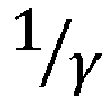
multiplication circuit 21 that scales an input audio signal by the adjustable factor ρ to produce the noise shaping input signal nshin. A dynamic range optimization (DYRO)control circuit 14 controls the adjustable factor ρ on the fly in an attempt to maximize the dynamic range and compensates thereceiver 15 accordingly by an adjustable factor α (e.g., an adjustable scaling factor). However, the multiplication which results from the error feedback arrangement within the noise shaper 4' causes the injection of a transient disturbance in the feedback, and this transient disturbance is propagated through to the output signal where it manifests as a transient audible phenomena referred to in the art as a "pop". - This can be observed in the graphs of the operation of the
audio playback circuit 1 shown inFIG. 3 , where transient disturbance in the output from the noise shaping circuit 4 (labelled as o_nsh), transient disturbance in the signal in thenoise shaping circuit 4 after re-quantization but prior to filtering (labelled as o_prefilt), and transient disturbance in the output of a filter within the noise shaping circuit 4 (labelled as o_filt), as shown for example by the output of an ITU filter labelled as itu), can be observed. As can be appreciated, this pop is undesirable, as the pop may be audible by the human ear. - As such, further development is needed.
- Disclosed herein is a signal processing circuit including a transmitter section. The transmitter section includes a noise shaper receiving a noise shaping input signal and a quantizer output signal, the noise shaper configured to generate a quantizer input signal based upon the noise shaping input signal and the quantizer output signal, and a quantizer receiving the quantizer input signal and configured to divide the quantizer input signal by a scaling factor to produce a noise shaping output signal and to multiply the noise shaping output signal by the scaling factor to product the quantizer output signal.
- The signal processing circuit also includes a receiver section, the receiver section including receiver circuitry receiving the noise shaping output signal, the receiver circuitry configured to scale the quantizer output signal by a second scaling factor, and a dynamic range optimization circuit. The dynamic range optimization circuit is configured to determine whether an absolute value of the noise shaping input signal is less than a threshold value, lower the scaling factor in response to the absolute value of the noise shaping input signal being less than the threshold value, and decrease the second scaling factor in response to the absolute value of the noise shaping input signal being less than the threshold value, proportionally to the lowering of the scaling factor such that a ratio between the scaling factor and the second scaling factor remains substantially constant.
- The dynamic range optimization circuit is further configured to increase the scaling factor in response to the absolute value of the noise shaping input signal being greater than the threshold value and increase the second scaling factor in response to the absolute value of the noise shaping input signalbeing greater than the threshold value, proportionally to the increase in the scaling factor such that the ratio between the scaling factor and second scaling factor remains substantially constant.
- A dither generator may be configured to generate a dither signal having a range defined by the scaling factor, and the transmitter section may include a summing circuit configured to inject the dither signal into the quantizer input signal prior to quantization thereof by the quantizer.
- The quantizer may apply a truncation to the quantizer input signal after division thereof by the scaling factor.
- The scaling factor may be a power of two.
- The quantizer input signal and quantizer output signal may be digital, and the quantizer may be implemented digitally.
- The quantizer input signal and quantizer output signal may be analog, and the quantizer may be implemented in an analog fashion, with the quantizer including an analog to digital converter (ADC) receiving the quantizer input signal and digitizing the quantizer input signal to produce the noise shaping output signal such that it is scaled by the scaling factor, and a digital to analog converter (DAC) receiving the noise shaping output signal and converting the noise shaping output signal to produce the quantizer output signal such that it is multiplied by the scaling factor.
- The receiver section may be implemented digitally.
- The receiver section may be implemented in an analog fashion.
- The noise shaper may include an input summer configured to subtract an error signal from the noise shaping input signal to produce the quantizer input signal, an error summer configured to subtract the quantizer input signal from the quantizer output signal to produce an intermediate output, and a noise shaping filter configured to apply a noise shaping filter function to the intermediate output to produce the error signal.
- The noise shaper may include a sigma delta modulator receiving the noise shaping input signal and the quantizer output signal as output and applying a two-input one-output filtering thereto to produce the quantizer input signal. The two-input one-output filtering may have a transfer function of:

- The absolute value of the noise shaping signal may be determined from a current value of the noise shaping input signal.
- Also disclosed herein is a signal processing method including generating a quantizer input signal based upon a noise shaping input signal and a quantizer output signal, dividing the quantizer input signal by a scaling factor to produce a noise shaping output signal, and multiplying the noise shaping output signal by the scaling factor to product the quantizer output signal. The method further includes scaling the quantizer output signal by a second scaling factor, determining whether an absolute value of the noise shaping input signal is less than a threshold value, lowering the scaling factor in response to the absolute value of the noise shaping input signal being less than the threshold value, and decreasing the second scaling factor in response to the absolute value of the noise shaping input signal being less than the threshold value, proportionally to the lowering of the scaling factor such that a ratio between the scaling factor and the second scaling factor remains substantially constant.
- The method may further include generating an analog output signal from at least the noise shaping output signal by selectively connecting or disconnecting current sources and current sinks to differential outputs in response to the noise shaping output signal (the current sources and current sinks being scaled by the second scaling factor), amplifying the analog output signal, and driving a speaker with the analog output signal. Adjustment of the scaling factor and the second scaling factor proportionally to one another may serve to prevent transients resulting from scaling factor adjustment from being present in the noise shaping output signal and therefore from causing audible pops to be played by the speaker.
- The method may include increasing the scaling factor in response to the absolute value of the noise shaping input signal being greater than the threshold value and increasing the second scaling factor in response to the absolute value of the noise shaping input signalbeing greater than the threshold value, proportionally to the increase in the scaling factor such that the ratio between the scaling factor and second scaling factor remains substantially constant.
- The method may include generating a dither signal having a range defined by the scaling factor and injecting the dither signal into the quantizer input signal prior to quantization thereof.
- The method may include applying a truncation to the quantizer input signal after division thereof by the scaling factor.
- The scaling factor may be a power of two.
-
-
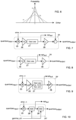
FIG. 1 is a block diagram of a first known noise shaping quantizer. -
FIG. 2 is a block diagram of a second known noise shaping quantizer. -
FIG. 3 includes a series of graphs showing values of signals in an audio playback circuit utilizing the known noise shaping quantizer ofFIG. 2 while performing audio signal scaling at the noise shaper input, compensating it into the receiver and into the noise shaper filter memory, with the occurrence of pop due to the audio signal scaling being visible. -
FIG. 4 is a block diagram of a first noise shaping variable quantizer broadly described herein. -
FIG. 5 is a block diagram of a first noise shaping variable quantizer broadly described herein, with dither that is scaled together with quantization. -
FIG. 6 is a graph showing how the probability distribution of the dither injected into the signal in the noise shaping variable quantizer ofFIG. 5 changes during operation with the scaling of the quantization. -
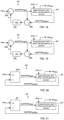
FIG. 7 is a block diagram showing an embodiment of the quantizer ofFIG. 5 in which the dither is subtracted prior to production of the quantizer output. -
FIG. 8 is a block diagram showing an embodiment of the quantizer ofFIG. 4 in which dither is not injected. -
FIG. 9 is a block diagram showing an embodiment of the quantizer ofFIG. 5 in which the quantizer is digital. -
FIG. 10 is a block diagram showing an embodiment of the quantizer ofFIG. 5 in which the quantizer is analog. -
FIG. 11 is a schematic block diagram showing specifics of the ADC and DAC of the analog quantizer ofFIG. 10 for use with a digital receiver section. -
FIG. 12A is a schematic block diagram showing first possible specifics of the ADC and DAC of the analog quantizer ofFIG. 10 for use with an analog receiver section. -
FIG. 12B is a schematic block diagram showing second possible specifics of the ADC and DAC of the analog quantizer ofFIG. 10 for use with an analog receiver section. -
FIG. 13 is a block diagram showing an embodiment of noise shaping variable quantizer described herein where the quantizer is digital and the receiver section is analog. -
FIG. 14 is a schematic block diagram of the current steering DAC ofFIG. 13 . -
FIG. 15 is a block diagram showing an embodiment of a noise shaping variable quantizer described herein where the quantizer is digital and the receiver section is digital as well. -
FIG. 16 is a block diagram showing an embodiment of a noise shaping variable quantizer described herein where the quantizer is analog and the receiver section is digital. -
FIG. 17 is a block diagram showing an embodiment of a noise shaping variable quantizer described herein where the quantizer and the receiver section are both analog. -
FIG. 18 is a block diagram showing the noise shaping filter of a digital quantizer described herein, the noise shaping filter utilizing error feedback. -
FIG. 19 is a block diagram showing the noise shaping filter of an analog quantizer described herein, the noise shaping filter utilizing error feedback. -
FIG. 20 is a block diagram showing the noise shaping filter of a digital quantizer described herein, the noise shaping filter utilizing sigma delta modulation. -
FIG. 21 is a block diagram showing the noise shaping filter of an analog quantizer described herein, the noise shaping filter utilizing sigma delta modulation. -
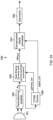
FIG. 22 is a schematic block diagram of a digital audio playback circuit described herein utilizing a digital noise shaping variable quantizer with error based feedback. -
FIG. 23 includes a series of graphs showing values of signals in the digital audio playback circuit ofFIG. 22 during operation. -
FIG. 24 is a block diagram of an analog to digital audio conversion circuit described herein. - The following disclosure enables a person skilled in the art to make and use the subject matter disclosed herein. The general principles described herein may be applied to embodiments and applications other than those detailed above without departing from the spirit and scope of this disclosure. This disclosure is not intended to be limited to the embodiments shown, but is to be accorded the widest scope consistent with the principles and features disclosed or suggested herein.
- Now described herein with initial reference to
FIG. 4 is a samplesignal processing chain 20 including a transmitter section (e.g., a noise shaping quantizer) 21 and a receiver section 35 (e.g., a digital to analog converter, DAC). Thetransmitter section 21 may be analog or digital, and thereceiver section 35 may be analog or digital. - Described now is a generic case, applicable to both analog and digital implementations. The
noise shaping quantizer 21 includes anoise shaping filter 23 that receives a noise shaping input signal nshin. Thenoise shaping filter 23 performs filtering and utilizes error feedback to produce a quantizer input signal quantizerinput. Aquantizer 24 receives the quantizer input signal quantizerinput and, under control of a dynamic range optimization circuit (DYRO control circuit) 34 as will be explained below, performs noise shaping and on-the-fly scaling on the noise shaping input signal nshin to produce a noise shaped output signal nshout. - The quantizer input signal quantizerinput is divided by an adjustable factor γ (e.g., a scaling factor) in a
divider 26. Atruncation circuit 27 operates on the output of thedivider 26, resulting in data loss, for example by rounding, saturation, or introducing of other non-linearities, producing the noise shaping output signal nshout. Afeedback multiplier 28 multiplies the noise shaping output signal nshout by the same adjustable factor γ to produce a quantizer output signal quantizeroutput provided to thenoise shaping filter 23 for use in performing noise shaping. Thereceiver section 35 multiplies the noise shaping output signal nshout by another adjustable factor α (e.g., a scaling factor) to produce an output signal OUT. The adjustablefactor γ and adjustable factor α may also be referred to as scaling factors herein. The different potential valuables of the adjustable factors γ and α may be represented by an index k, for example, γk and αk. - The
DYRO control circuit 34 monitors the noise shaping input signal nshin and based upon the amplitude thereof, adjusts the adjustable factor γ and the adjustable factor α on the fly so as to balance output signal OUT swing with its quantization noise, as will be described below, with such adjusting maintaining the ratio
- There are physical limits to the
divider 26 and thefeedback multiplier 28, as well as to thereceiver section 35, that limits the output signal OUT swing. To work within these constraints, theDYRO control circuit 34 compares the noise shaping input signal nshin to a series of accurately defined thresholds, and sets the adjustable factor γ and the adjustable factor α on the fly based upon those comparisons. - In detail, γ and α may each take one of i different values. As a first order approximation, the following relationship is present:

- For a given maximum value of the absolute value of the noise shaping output signal nshout, denoted as nshout
max (which is set by limits inherent to the implementation of the quantizer 24), the following relationship is therefore present:
nshinmax (i) is therefore the maximum of the absolute value of the noise shaping input nshin at the value of γi . - Assume, as an example, that i=1, ..., 3. Therefore, γi = [γ 1;γ 2;γ 3], with γ 1 > γ 2 > γ 3, and ai = [α1; α 2; α 3], with α 1 > α 2 > α 3, and with those values being such that

- During operation, the
DYRO control circuit 34 compares the current value (e.g., a current value) of the noise shaping input signal nshin to the thresholds TH 1, TH 2, and TH 3. If the noise shaping input signal nshin is greater than TH 1, then the adjustable factors are set by theDYRO control circuit 34 as follows:
- If the noise shaping input signal nshin is greater than TH 2 but less than TH 1, then the adjustable factors are set by the
DYRO control circuit 34 as follows:
- If the noise shaping input signal nshin is greater than TH 3 but less than TH 2, then the adjustable factors are set by the
DYRO control circuit 34 as follows:
- If i were to be greater than 3, then additional thresholds and adjustable factors would be present, and further comparisons consistent with the above described comparisons would be performed.
- The result of this above-described operation is that the quantizer output quantizeroutput will practically have the same amplitude as the quantizer quantizerinput while the quantization noise will be reduced.
- These comparison and adjustable factor setting operations are performed continuously or periodically on the noise shaping input signal nshin, and therefore the adjustment of the adjustable factors γ and α is performed continuously or periodically. The result of this is that the output signal OUT will practically have the same amplitude while quantization noise present at the
receiver section 35 OUT will be reduced - thus, dynamic range at OUT is increased. - In some implementation instances, the
DYRO control circuit 34 may implement a margin in its thresholds and therefore in its threshold comparisons. The margin value is greater than zero but less than one. The thresholds can be calculated as:
- Time filtering may be performed on the threshold comparisons by the
DYRO control circuit 34 in the falling direction. In the falling direction (such as when the noise shaping input signal nshin was previously greater than TH 1, but is now less than TH 1 and greater than TH 2) for example, theDYRO control circuit 34 may wait to take action to change the adjustable factor γ and the adjustable factor α until after the noise shaping input signal nshin has fallen below and remained below the threshold in question (e.g., has fallen below TH 1) for a given period of time. Such time filtering may optionally be performed in the rising direction (such as when the noise shaping input signal nshin was previously less than TH 1 and greater than TH 2, but is now greater than TH 1) as well, although this may not be desired in some situations. - Further details of the principles of operation of the
DYRO control circuit 34 may be found inUnited States Patent No. 7,239,258 , incorporated by reference above. - Optionally, as shown in the embodiment of
FIG. 5 , the dither signal dither_in is generated by adither circuit 38 under control of theDYRO control circuit 34 according to changes made to the adjustable factor γ. Dithering prevents correlation between the quantization noise and the desired information represented by the output signal OUT. - In instances where the
quantizer 24 is digital, the injected dither may have a triangular probability distribution function as shown inFIG. 6 , with the specific shape of the probability distribution function changing with γ. Details of this type of dithering may be found in Digital Dither, S. P. Lipshitz and, J. Vanderkooy, In Audio Engineering Society Convention 81, Nov 1986, the contents of which are incorporated by reference in their entirety. - The injected dither may instead have a rectangular probability function, also in instances where the
quantizer 24 is digital. In instances where thequantizer 24 is analog, thedither circuit 38, under control of theDYRO control circuit 34, may supply the dither signal dither_in as two random analog values. - In the example
generic quantizer 24 described above, the dither signal dither_in is injected to the quantizer input quantizerinput prior to operation thereon by thedivider 26, but is not subtracted from the quantizer output quantizeroutput. However, as shown in the example ofFIG. 7 , thequantizer 24 may include asubtractor 24 that subtracts the dither signal dither_in from the quantizer output quantizeroutput. - The dither signal dither_in in embodiments in which the
quantizer 24 is digital, the dither signal may be generated through the sum of two linear feedback shift registers (LFSRs), or as the sum of two separated branches of a single LFSR. The dither signal may be generated through any suitable circuit, and may take any suitable form. - In the above example
generic quantizer 24, dither is injected. However, as shown inFIG. 8 , thequantizer 24 may not include dither injection, and the quantizer input quantizerinput may be directly fed to thedivider 26. - In the above example, the
transmitter section 21 is described generically, and such description of operation applies to either an analog or a digital transmitter section. Also in the above example, thereceiver section 35 is described generically, and such description of operation applies to either an analog ordigital receiver section 35. With this being said, specific examples will be provided below, in which: - 1. The
transmitter section 21 is digital and thereceiver section 35 is analog; - 2. The
transmitter section 21 is digital and thereceiver section 35 is digital; - 3. The
transmitter section 21 is analog and thereceiver section 35 is digital; and - 4. The
transmitter section 21 is analog and thereceiver section 35 is analog. - Each of these will be described, but first, digital and analog quantizers for use therein will be described. Note that any digital functions or components described herein may be incorporated within a microprocessor, digital signal processor, or programmable logic device, and any analog functions or components described herein may be incorporated within discrete analog components.
- A sample digital quantizer 24' is shown in
FIG. 9 and has the structure and function of thedigital quantizer 24 described above. In this sample digital quantizer 24', the adjustable factor γ is equal to 2 β , and therefore thedivider 26 performs a division of the quantizer input quantizerinput (after dither injection) 2 β , while thefeedback multiplier 28 multiplies the noise shaping output nshout by 2 β . Here, thedata loss function 27 may be a round, floor, or ceiling function, for example. Note that it is possible in a digital implementation of the quantizer 24' for the adjustable factor γ to instead be implemented as a ratio of two integers or as a floating point value, depending upon hardware. - A sample
generic analog quantizer 24" is shown inFIG. 10 . Theanalog quantizer 24" includes asummer 25 through which an analog dither signal dither_in is injected into the analog quantizer input signal quantizerinput prior to analog to digital conversion by an analog to digital converter (ADC) 26'. During the analog to digital conversion, an effective division of the quantizer input signal quantizerinput by the adjustable factor γ is performed. The output of the ADC 26' is the noise shaping output nshout. A digital to analog converter (DAC) 28' converts the noise shaping output nshout back to analog form, and performs an effective multiplication of the noise shaping output nshout by the adjustable factor γ to produce an analog quantizer output signal quantizeroutput. - One potential implementation of the
analog quantizer 24" which is intended for use with adigital receiver section 35 is shown inFIG. 11 . In this implementation, the ADC 26' is arranged to be used to generate k thresholds for use in analog to digital conversion. To that end, a resistor ladder is connected between a positive voltage +Vγ and a negative voltage -Vγ , with these voltages having equal and opposite magnitudes set as a function of the current value of the adjustable factor γ. The voltage ladder is formed by m resistors (m being equal to 2k+1) connected in series between +Vγ and -Vγ , and generates k positive threshold voltages and k negative threshold voltages. The magnitudes of the threshold voltages can be represented as:
- As illustrated, threshold voltages VTH1, ..., VTHk and -VTH1, ..., -VTHk are generated at taps between the resistors of the voltage ladder. The resistor directly connected to +Vγ has a resistance of

- The ADC 26' in this
analog quantizer 24" shown inFIG. 11 includes 2k comparators, here shown as comparators 41(1), ..., 41(2k), providing output to 2k flip flops, here shown as flip flops 42(1), ..., 42(2k). The flip flops 42(1), ..., 42(2k) provide their outputs as selection signals to 2k switch circuits, here shown as switch circuits 44(1), ..., 44(2k). - The comparators 41(1), ..., 41(2k) each have a non-inverting input terminal coupled to receive the quantizer input signal quantizerinput, which is an analog voltage Vquantizer_in in this instance. The comparators 41(1), ..., 41(2k) have respective inverting input terminals connected to different ones of the threshold voltages VTH1, ..., VTHk and -VTH1, ..., -VTHk. In the illustrated example, comparator 41(1) has its inverting input terminal connected to the threshold voltage VTHk, comparator 41(2) has its inverting input terminal connected to the threshold voltage VTH1, comparator 41(3) has its inverting input terminal connected to the threshold voltage -VTH1, and comparator 41(2k) has its inverting input terminal connected to the threshold voltage -VTHk. The flip flop 42(1) has its input receiving the output of the comparator 41(1) and has its output connected to provide a selection signal to the switch circuit 44(1), the flip flop 42(2) has its input receiving the output of the comparator 41(2) and has its output connected to provide a selection signal to the switch circuit 44(2), flip flop 42(3) has its input receiving the output of the comparator 41(3) and has its output connected to provide a selection signal to the switch circuit 44(3), and flip flop 42(2k) has its input receiving the output of the comparator 41(2k) and has its output connected to provide a selection signal to the switch circuit 44(2k).
- Each switch circuit 44(1), ..., 44(2k) operates to selectively connect an associated resistor (each such resistor having a resistance of R1) between either +Vγ or -Vγ and an inverting input terminal of an
amplifier 45, under control of the output of a respective flip flop 42(1), ..., 42(2k). When the output of a respective flip flop 42(1), ..., 42(2k) is asserted, the associated switch circuit 44(1), ..., 44(2k) connects its respective resistor to -Vγ and otherwise connects its respective resistor to Vγ . - The
amplifier 45 has its non-inverting input terminal grounded, and a resistor R2 is connected between the inverting input terminal and output of theamplifier 45. The output of theamplifier 45 is the quantizer output quantizeroutput, which is an analog voltage V quantizer_out in this instance. - The relationship in resistance value between R1 and R2 is as follows:

- The output of each flip flop 42(1), ..., 42(2k) is also connected to circuit 46 (illustratively a thermometric to signed
converter 46 that generates the noise shaping output nshout in digital form therefrom). - As stated, the voltages +Vγ and -Vγ are based upon the adjustable factor γ. For example, the voltages +Vγ and -Vγ may be generated by a programmable voltage generator, with Vγ depending on the adjustable factor γ (e.g., where the adjustable factor γ changes from γ1 to γ2, Vγ changes from V y1 to V y2).
- As another example, the ADC 26' and DAC 28' may be integrated within a noise shaper utilizing either an error feedback or sigma-delta modulator arrangement.
- A first potential implementation of the
analog quantizer 24" which is intended for use with ananalog receiver section 35 is shown inFIG. 12A . The difference in thisanalog quantizer 24" over that shown inFIG. 11 is that the converter 46' in this instance includes 2k switch circuits 47(1), ..., 47(2k) respectively connected to receive the outputs of flip flops 42(1), ..., 42(2k) as respective selection signals. The output of the flip flops 42(1), ..., 42(2k) here forms the noise shaping output nshout. - Each switch circuit 47(1), ..., 47(2k) operates to selectively connect an associated resistor (each such resistor having a resistance of R3) between either +Vα or -Vα and a non-inverting input terminal of an
amplifier 48, under control of the output of a respective flip flop 42(1), ..., 42(2k). When the output of a respective flip flop 42(1), ..., 42(2k) is asserted, the associated switch circuit 47(1), ..., 47(2k) connects its respective resistor to -Vα and otherwise connects its respective resistor to Vα. - The voltages +Vα and -Vα are based upon the adjustable factor α. For example, the voltages +V, and -Vα may be generated by a programmable voltage generator, with Vα depending on the adjustable factor α (e.g., where the adjustable factor α changes from α1 to α2, Vα changes from V α1 to V α2).
- The
amplifier 48 has its non-inverting input terminal grounded, and a resistor R4 is connected between the inverting input terminal and output of theamplifier 48. The output of theamplifier 48 may be used for desired purposes. - The relationship in resistance value between R3 and R4 is as follows:

- A second potential implementation of the
analog quantizer 24" is shown inFIG. 12B . The difference here is that the noise shaping output nshout is produced at the output of theamplifier 48 as an analog voltage to be fed to the receiver 35', and here the receiver 35' is not scaled by the adjustable factor α because that scaling is performed by the converter 46'. - A
signal processing chain 100 is shown inFIG. 13 which includes a noise shaping digital quantizer as adigital transmitter section 22 and ananalog receiver section 35. The noise shapingdigital quantizer 22 operates as described above with reference toFIGS. 4, 5 , and9 and needs no further description herein. - The
analog receiver section 35 includes acurrent steering DAC 150 that converts the noise shaping output signal nshout to produce an analog output signal Aout. Thecurrent steering DAC 150 includes a thermometric code conversion circuit that selects elementary contributions to the analog output signal Aout that are scaled by the adjustable factor α. Alow pass filter 151 filters quantization noise from the analog output signal Aout, and the analog output signal Aout is then amplified by apower amplifier 152 that drives aspeaker 153 or other output device. - An example implementation of the
current steering DAC 150 is now described with additional reference toFIG. 14 . TheDAC 150 may be any suitable type of DAC, however, as an example, the illustratedDAC 150 is a current steering DAC that receives the noise shaping output signal nshout as input. - The
DAC 150 provides differential current outputs generated by N=2 n respective current sources and current sinks that are selectively connected to the input by switches based upon the noise shaping output signal nshout , with n being, for example, 6 such that 2 n = 64. The current sources and current sinks each respectively source or sink a current Iref having a same magnitude multiplied by α. Stated differently, these currents are equal and each changed in magnitude proportionally to the current reference. - For example, where n=6, and therefore, N=26=64, there are 64 current sources and 64 current sinks in the
DAC 150. The current sources are labeled inFIG. 14 as sourcing currents α · Iref 1, ..., α · IrefN and the current sinks are labeled inFIG. 14 as sinking currents α · Iref 1, ..., α · IrefN. - A signal processing chain 100' is shown in
FIG. 15 which includes a noise shaping digital quantizer 24' as adigital transmitter section 22 and adigital receiver section 35. The noise shapingdigital quantizer 22 operates as described above with reference toFIGS. 4, 5 , and9 and needs no further description herein. - The
digital receiver section 35 includes ascaling circuit 154 that scales the noise shaping output nshout by α to produce a digital output signal Dout. The digital output signal Dout is thereafter passed through a decimating low-pass filter 155 and then adigital elaboration circuit 156. - A
signal processing chain 101 is shown inFIG. 16 which includes ananalog quantizer 24" as ananalog transmitter section 22 and adigital receiver section 35. Theanalog quantizer 24" operates as described above with reference toFIGS. 10 ,11 ,12 and needs no further description herein. - The
digital receiver section 35 includes ascaling circuit 154 that multiplies the noise shaping output nshout by α (with α ≥ 1 or α < 1) to produce a digital output signal Dout. The digital output signal Dout is thereafter passed through a decimating low-pass filter 155 and then adigital elaboration circuit 156. - A signal processing chain 101' is shown in
FIG. 17 which includes ananalog quantizer 24" as ananalog transmitter section 22 and ananalog receiver section 35. Theanalog quantizer 24" operates as described above with reference toFIGS. 10 ,12 and needs no further description herein. - The
analog transmitter section 22 operates as described above with reference toFIG. 12 and needs no further description herein. - The
noise shaping filter 23 used in the above-described embodiments may utilize error feedback or sigma-delta modulation. - Now described with reference to
FIG. 18 is an embodiment of thenoise shaping filter 23 utilizing error feedback and designed to work with a digital quantizer 24'. Thenoise shaping filter 23 includes aninput summer 23a that subtracts an error signal err output by anoise shaping filter 23c from the noise shaping input signal nshin to produce the quantizer input quantizerinput. The digital quantizer 24' injects the dither signal dither in to the quantizer input quantizerinput and divides the quantizer input quantizerinput by the adjustable factor γ (which in this instance may be 1/2β), with that result being truncated such as by a rounding, floor, or ceiling function to produce the noise shaping output signal nshout. The digital quantizer 24' multiplies the noise shaping output signal nshout to produce the quantizer output quantizeroutput. Anerror summer 23b subtracts the quantizer input quantizerinput from the quantizer output quantizeroutput and provides the result to thenoise shaping filter 23c which has a transfer function of H(z). Thenoise shaping filter 23c produces the error signal err as output. - The above-described error feedback arrangement may also be used with an
analog quantizer 24", as shown inFIG. 19 , and operating as described above with reference toFIG. 18 . - Now described with reference to
FIG. 20 is an embodiment of the noise shaping filter 23' in which the noise shaping filter is implemented as a sigma-delta modulator 23a', and designed to work with a digital quantizer 24'. The sigma-delta modulator 23a' includes a U-input (L 0) that receives the noise shaping input nshin and a V-input (L 1) that receives the quantizer output quantizeroutput, and the output of the sigma-delta modulator 23a' is the quantizer input quantizerinput. The sigma-delta modulator 23a' applies a two-input, one output filtering according to the equation Y(z) = L 0(z)U(z) - L 1(z)V(z). The quantizer input quantizerinput may be produced as a digital signal for use with the digital quantizer 24' (FIG. 20 ), ormay be produced as an analog signal for use with theanalog quantizer 24" (FIG. 21 ). - Sample sigma-delta modulator designs such as may be used in the embodiment of
FIG. 20 may be found in Understanding Delta-Sigma Delta Data Converters, Pavan, Shanthi; Schreir, Richard; Temes, Gabor C., IEEE Press Series on Microelectronic Systems, IEEE 2017, the contents of which are incorporated by reference. - Now described with reference to
FIG. 22 is asignal processing chain 100 utilized as an audio output circuit. In thissignal processing chain 100, thetransmitter section 21 includes a digital quantizer 24' and error feedback basednoise shaping circuit 23 as described above, and the receiver section includes acurrent steering DAC 150 as described above - During operation, the
DYRO control circuit 14 compares the values of the noise shaping input nshin to a series of thresholds, and based thereupon, adjusts the adjustable factor γ and the adjustable factor α on the fly, with such adjusting maintaining the ratio
- The thresholds for this example will now be discussed. Assume here that the
noise shaping filter 23c is a finite impulse response filter with coefficients fircoeffk. The relationship between the maximum noise shaping input nshinmax and the maximum noise shaping output nshoutmax can be mathematically represented as:
- An expression factori may be written as:

- Therefore, nshin (i) can be written as:

- The thresholds can then be set as follows, assuming margin is used:

- Example operation is now described with additional reference to
FIG. 23 . Assume in this case that the noise shaping input signal nshin is 24 bit, and the noise shaping output signal nshout is 7 bit. Initially, assume the adjustable factor γ to be set to:
- Assume the current reference Iref used by the
DAC 15 is 1 µA. Prior to time T1, the input audio signal i_audio (which is interpolated to produce the noise shaping input nshout ) is playing audio and not muted. At time T1, the input audio signal i_audio is muted, and the noise shaping at the output nshout of thenoise shaping circuit 23 can be observed between times T1 and T2. The quantization noise prior to filtering within thenoise shaping circuit 23 can be observed between times T1 and T2 as o_prefilt, and after filtering can observed between times T1 and T2 as o_filt. - At time T2, nshin is below the first threshold for the given period of time, and therefore the β is reduced to 16 by the
DYRO control circuit 14, so the adjustable factor γ is set such that:
- Since β is being reduced by one, the
DYRO control circuit 14 adjusts the reference current Iref within theDAC 14 accordingly by properly scaling α (keeping in mind that
noise shaping circuit 23 can be observed between times T2 and T3 as o_prefilt, and after filtering can observed between times T2 and T3 as o_filt. - At time T3, nshin is below the second threshold (which is lower than the first threshold), and therefore β is reduced to 15 by the
DYRO control circuit 14. Since the adjustable factor β is being reduced by one, theDYRO control circuit 14 adjusts the reference current α · Iref within theDAC 14 accordingly, which in this case is a reduction from ½ µA to ¼ µA. The further reduction of the quantization noise prior to filtering within thenoise shaping circuit 23 can be observed after time T3 as o_prefilt, and after filtering can observed after time T3 as o_filt. - Observe that at the changing of the adjustable factor β at times T2 and T3, there is no occurrence of a transient disturbance which would manifest as an audible "pop".
- Although not expressly shown on in the graph of
FIG. 23 , note that the dither is adjusted according to the adjustable factor γ. For example, according to this specific embodiment where γ = 2β, the dither range may be from [-2β, 2β], with a triangular probability distribution, and with β being changed as the adjustable factor γ is changed. - The above dynamic range expansion performed through the use of variable scaling of re-quantization during digital to analog conversion is equally applicable to analog to digital conversion. To that end, an embodiment of an
audio sampling circuit 200 using variable scaling of re-quantization during analog to digital conversion is now described with reference toFIG. 24 . - The
audio sampling circuit 200 includes amicrophone 201 receiving input sound waves and converting them to an analog audio signal, which is then preconditioned by apreconditioning amplifier 202 to produce an analog audio input signal Ain . Thepreconditioning amplifier 202 may have a low-pass filtering behavior because the noise shaping input signal nshin is within a limited bandwidth range. Anoise shaping converter 203, here a sigma-delta based analog to digital converter controlled based upon the adjustable factor γ, receives the analog audio input signal Ain and digitizes the analog audio input signal Ain to produce the noise shaping input signal nshin, which is then compensated by acompensation circuit 204 according to the adjustable factor α, and in turn decimated by adecimation filter 205 to produce output that may be used for suitable purposes, for example by a digital elaboration unit for further processing, for example in a wave file writing system. TheDYRO control circuit 206 operates as described above, comparing the analog input signal Ain to the thresholds and adjusting the adjustable factors γ and α accordingly. - It is clear that modifications and variations may be made to what has been described and illustrated herein, without thereby departing from the scope of this disclosure, as defined in the annexed claims.
- While the disclosure has been described with respect to a limited number of embodiments, those skilled in the art, having benefit of this disclosure, will appreciate that other embodiments can be envisioned that do not depart from the scope of the disclosure as disclosed herein. Accordingly, the scope of the disclosure shall be limited only by the attached claims.
Claims (15)
- A signal processing circuit (20), comprising:
a transmitter section (21) including a noise shaper (23), the noise shaper comprising:a filter (23) receiving a noise shaping input signal (nshin) and a quantizer output signal (quantizeroutput), the filter (23) configured to generate a quantizer input signal (quantizerinput) based at least upon the noise shaping input signal (nshin) and the quantizer output signal (quantizeroutput); anda quantizer (24) receiving the quantizer input signal (quantizerinput) and configured to divide the quantizer input signal (quantizerinput) by a first scaling factor (γ) to produce a noise shaping output signal (nshout), and to multiply the noise shaping output signal (nshout) by the first scaling factor (γ) to produce the quantizer output signal (quantizeroutput);a receiver section (35) including:receiver circuitry (35) receiving the noise shaping output signal (nshout), the receiver circuitry (35) configured to scale the quantizer output signal (quantizeroutput) by a second scaling factor (α);a dynamic range optimization circuit (34) configured to:determine whether an absolute value of the noise shaping input signal (nshin) is less than a threshold value;lower the first scaling factor (γ) in response to the absolute value of the noise shaping input signal (nshin) being less than the threshold value;decrease the second scaling factor (α) in response to the absolute value of the noise shaping input signal (nshin) being less than the threshold value, proportionally to the lowering of the first scaling factor (γ) such that a ratio between the first scaling factor (γ) and the second scaling factor (α) remains substantially constant. - The signal processing circuit (20) of claim 1, wherein the noise shaping input signal (nshin) represents audio data; and wherein the receiver section (35) comprises:a current steering digital to analog converter, DAC (150) configured to generate an analog output signal (Aout) from the noise shaping output signal (nshout) by selectively connecting or disconnecting current sources (αIref1) and current sinks (αIref1) to differential outputs in response to the noise shaping output signal (nshout), the current sources and current sinks being scaled by the second scaling factor (α);a power amplifier (152) configured to amplify the analog output signal; anda speaker (153) driven by the analog output signal;wherein adjustment of the first scaling factor (γ) and the second scaling factor (α) by the dynamic range optimization circuit (34) proportionally to one another serves to prevent transients resulting from scaling factor adjustment from being present in the noise shaping output signal (nshout) and therefore from causing audible pops to be played by the speaker.
- The signal processing circuit (20) of claim 1, wherein the dynamic range optimization circuit (34) is further configured to increase the first scaling factor (γ) in response to the absolute value of the noise shaping input signal (nshin) being greater than the threshold value and increase the second scaling factor (α) in response to the absolute value of the noise shaping input signal (nshin) being greater than the threshold value, proportionally to the increase in the first scaling factor (γ) such that the ratio between the first scaling factor (γ) and second scaling factor (α) remains substantially constant.
- The signal processing circuit (20) of claim 1, further comprising a dither generator (38) configured to generate a dither signal (dither_in) having a range defined by the first scaling factor (γ); and wherein the transmitter section (21) includes a summing circuit (25) configured to inject the dither signal into the quantizer input signal (quantizerinput) prior to quantization thereof by the quantizer (24').
- The signal processing circuit (20) of claim 1,wherein the quantizer (24) applies a truncation to the quantizer input signal (quantizerinput) after division thereof by the first scaling factor (γ).
and/orwherein the first scaling factor (γ) is a power of two,and/orwherein the quantizer input signal (quantizerinput) and quantizer output signal (quantizeroutput) are digital; and wherein the quantizer (24) is implemented digitally. - The signal processing circuit (20) of claim 1, wherein the quantizer input signal (quantizerinput) and quantizer output signal (quantizeroutput) are analog; and wherein the quantizer (24) is implemented in an analog fashion, with the quantizer (24) comprising:an analog to digital converter, ADC (26) receiving the quantizer input signal (quantizerinput) and digitizing the quantizer input signal (quantizerinput) to produce the noise shaping output signal (nshout) such that it is scaled by the first scaling factor (γ); anda digital to analog converter, DAC (150) receiving the noise shaping output signal (nshout) and converting the noise shaping output signal (nshout) to produce the quantizer output signal (quantizeroutput) such that it is multiplied by the first scaling factor (γ).
- The signal processing circuit (20) of claim 1, wherein:the receiver section (35) is implemented digitally,
orthe receiver section (35) is implemented in an analog fashion. - The signal processing circuit (20) of claim 1, wherein the filter (23) comprises:an input summer (23a) configured to subtract an error signal (err) from the noise shaping input signal (nshin) to produce the quantizer input signal (quantizerinput);an error summer (23b) configured to subtract the quantizer input signal (quantizerinput) from the quantizer output signal (quantizeroutput) to produce an intermediate output; anda noise shaping filter (23) configured to apply a noise shaping filter function to the intermediate output to produce the error signal (err).
- The signal processing circuit (20) of claim 1, wherein the filter (23) comprises: a sigma delta modulator (23a') receiving the noise shaping input signal (nshin) and the quantizer output signal (quantizeroutput) as output and applying a two-input one-output filtering thereto to produce the quantizer input signal (quantizerinput), wherein the two-input one-output filtering preferably has a transfer function of:

- The signal processing circuit (20) of claim 1, wherein the absolute value of the noise shaping signal is determined from a current value of the noise shaping input signal (nshin).
- A signal processing method, comprising:generating a quantizer input signal (quantizerinput) based at least upon a noise shaping input signal (nshin) and a quantizer output signal (quantizeroutput); anddividing the quantizer input signal (quantizerinput) by a first scaling factor (γ) to produce a noise shaping output signal (nshout), and multiplying the noise shaping output signal (nshout) by the first scaling factor (γ) to produce the quantizer output signal (quantizeroutput);scaling the quantizer output signal (quantizeroutput) by a second scaling factor (α);determining whether an absolute value of the noise shaping input signal (nshin) is less than a threshold value;lowering the first scaling factor (γ) in response to the absolute value of the noise shaping input signal (nshin) being less than the threshold value; anddecreasing the second scaling factor (α) in response to the absolute value of the noise shaping input signal (nshin) being less than the threshold value, proportionally to the lowering of the first scaling factor (γ) such that a ratio between the first scaling factor (γ) and the second scaling factor (α) remains substantially constant.
- The method of claim 11, further comprising:generating an analog output signal (Aout) from the noise shaping output signal (nshout) by selectively connecting or disconnecting current sources (αIref1) and current sinks (αIref1) to differential outputs in response to the noise shaping output signal (nshout), the current sources and current sinks being scaled by the second scaling factor (α);amplifying the analog output signal (Aout); anddriving a speaker (153) with the analog output signal (Aout);wherein adjustment of the first scaling factor (γ) and the second scaling factor (α) proportionally to one another serves to prevent transients resulting from scaling factor adjustment from being present in the noise shaping output signal (nshout) and therefore from causing audible pops to be played by the speaker.
- The method of claim 11, further comprising:
increasing the first scaling factor (γ) in response to the absolute value being greater than the threshold value and increasing the second scaling factor (α) in response to the absolute value being greater than the threshold value, proportionally to the increase in the first scaling factor (γ) such that the ratio between the first scaling factor (γ) and second scaling factor (α) remains substantially constant. - The method of claim 11, further comprising generating a dither signal (dither_in) having a range defined by the first scaling factor (γ); and injecting the dither signal into the quantizer input signal (quantizerinput) prior to quantization thereof.
- The method of claim 11:further comprising applying a truncation (27) to the quantizer input signal (quantizerinput) after division thereof by the first scaling factor (γ),
and/orwherein the first scaling factor (γ) is a power of two.
Applications Claiming Priority (1)
| Application Number | Priority Date | Filing Date | Title |
|---|---|---|---|
| US17/846,520 US12003247B2 (en) | 2022-06-22 | 2022-06-22 | Noise shaper variable quantizer |
Publications (1)
| Publication Number | Publication Date |
|---|---|
| EP4297279A1 true EP4297279A1 (en) | 2023-12-27 |
Family
ID=86603852
Family Applications (1)
| Application Number | Title | Priority Date | Filing Date |
|---|---|---|---|
| EP23175324.5A Pending EP4297279A1 (en) | 2022-06-22 | 2023-05-25 | Noise shaper variable quantizer |
Country Status (3)
| Country | Link |
|---|---|
| US (1) | US12003247B2 (en) |
| EP (1) | EP4297279A1 (en) |
| CN (1) | CN117278030A (en) |
Citations (3)
| Publication number | Priority date | Publication date | Assignee | Title |
|---|---|---|---|---|
| US5252973A (en) * | 1991-07-03 | 1993-10-12 | Sony Corporation | Apparatus for digital-to-analogue conversion |
| US7239258B2 (en) | 2005-02-10 | 2007-07-03 | Stmicroelectronics S.R.L. | Enhancement of the dynamic range of a multibit digital-to-analog converter |
| EP3001569A1 (en) * | 2014-09-04 | 2016-03-30 | Analog Devices Global | Embedded overload protection in delta-sigma analog-to-digital converters |
Family Cites Families (8)
| Publication number | Priority date | Publication date | Assignee | Title |
|---|---|---|---|---|
| US6462685B1 (en) * | 2001-04-05 | 2002-10-08 | Nokia Corporation | Dither signal insertion inversely proportional to signal level in delta-sigma modulators |
| US7183954B1 (en) | 2001-07-13 | 2007-02-27 | Cirrus Logic, Inc. | Circuits, systems and methods for volume control in low noise 1-bit digital audio systems |
| US7671774B2 (en) * | 2008-05-08 | 2010-03-02 | Freescale Semiconductor, Inc. | Analog-to-digital converter with integrator circuit for overload recovery |
| US7961125B2 (en) | 2008-10-23 | 2011-06-14 | Microchip Technology Incorporated | Method and apparatus for dithering in multi-bit sigma-delta digital-to-analog converters |
| US9319051B2 (en) | 2013-05-28 | 2016-04-19 | Broadcom Corporation | Digital PLL with hybrid phase/frequency detector and digital noise cancellation |
| US8890727B1 (en) * | 2013-06-07 | 2014-11-18 | Mediatek Singapore Pte. Ltd. | Analog-to-digital converter circuit, integrated circuit, electronic device and method therefor |
| DE102013108573A1 (en) | 2013-08-08 | 2015-02-12 | Infineon Technologies Ag | Methods and devices for analog-to-digital conversion |
| EP3248291A4 (en) | 2015-01-22 | 2018-08-29 | John Howard La Grou | Multi-path, series-switched, passively-summed digital-to-analog converter |
-
2022
- 2022-06-22 US US17/846,520 patent/US12003247B2/en active Active
-
2023
- 2023-05-25 EP EP23175324.5A patent/EP4297279A1/en active Pending
- 2023-06-14 CN CN202310704877.8A patent/CN117278030A/en active Pending
Patent Citations (3)
| Publication number | Priority date | Publication date | Assignee | Title |
|---|---|---|---|---|
| US5252973A (en) * | 1991-07-03 | 1993-10-12 | Sony Corporation | Apparatus for digital-to-analogue conversion |
| US7239258B2 (en) | 2005-02-10 | 2007-07-03 | Stmicroelectronics S.R.L. | Enhancement of the dynamic range of a multibit digital-to-analog converter |
| EP3001569A1 (en) * | 2014-09-04 | 2016-03-30 | Analog Devices Global | Embedded overload protection in delta-sigma analog-to-digital converters |
Non-Patent Citations (2)
| Title |
|---|
| CONVERTERS, PAVAN, SHANTHISCHREIR, RICHARDTEMES, GABOR C.: "IEEE Press Series on Microelectronic Systems", 2017, IEEE |
| DIGITAL DITHERS. P. LIPSHITZJ. VANDERKOOY, AUDIO ENGINEERING SOCIETY CONVENTION, vol. 81, November 1986 (1986-11-01) |
Also Published As
| Publication number | Publication date |
|---|---|
| US20230421167A1 (en) | 2023-12-28 |
| US12003247B2 (en) | 2024-06-04 |
| CN117278030A (en) | 2023-12-22 |
Similar Documents
| Publication | Publication Date | Title |
|---|---|---|
| US6414613B1 (en) | Apparatus for noise shaping a pulse width modulation (PWM) signal and method therefor | |
| EP3229371B1 (en) | Audio amplifier system | |
| US8742970B2 (en) | Analogue-to-digital converter | |
| US7535392B2 (en) | Delta sigma modulator and method for compensating delta sigma modulators for loop delay | |
| EP0978165A1 (en) | Delta-sigma pwm dac for reduced switching | |
| JP3425344B2 (en) | D / A converter | |
| US8681029B1 (en) | Chopper-stabilization method and apparatus for sigma delta modulators | |
| CN100514858C (en) | Word length reduction circuit | |
| US10566993B2 (en) | Delta-sigma modulator and delta-sigma converter | |
| US6256395B1 (en) | Hearing aid output clipping apparatus | |
| US12003247B2 (en) | Noise shaper variable quantizer | |
| JP2002314425A (en) | Delta-sigma modulation apparatus and method, and digital signal processing apparatus and method | |
| WO2007094255A1 (en) | D/a converter | |
| EP1653605B1 (en) | Noise shaper for shaping a power spectral density of an error signal and method therefor | |
| US7423566B2 (en) | Sigma-delta modulator using a passive filter | |
| US11764803B2 (en) | D/A conversion device, method, storage medium, electronic musical instrument, and information processing apparatus | |
| CN114095030B (en) | Sigma-delta ADC for eliminating full-differential band string sounds | |
| JP3453279B2 (en) | Method and apparatus for controlling volume of 1-bit digital signal | |
| EP4451568A1 (en) | Delta-sigma modulator with anti-windup circuit | |
| JP3407851B2 (en) | Delta-sigma D / A converter with PWM circuit / weighting circuit combination | |
| US20240007128A1 (en) | Analog-to-digital conversion circuit | |
| JP3428412B2 (en) | Delta sigma A / D converter | |
| KR20190134932A (en) | Time domain continuous-time delta-sigma modulator and method of driving the same | |
| JP2018533302A (en) | Analog signal generator and related uses | |
| JP2000236259A (en) | D / A converter |
Legal Events
| Date | Code | Title | Description |
|---|---|---|---|
| PUAI | Public reference made under article 153(3) epc to a published international application that has entered the european phase |
Free format text: ORIGINAL CODE: 0009012 |
|
| STAA | Information on the status of an ep patent application or granted ep patent |
Free format text: STATUS: THE APPLICATION HAS BEEN PUBLISHED |
|
| AK | Designated contracting states |
Kind code of ref document: A1 Designated state(s): AL AT BE BG CH CY CZ DE DK EE ES FI FR GB GR HR HU IE IS IT LI LT LU LV MC ME MK MT NL NO PL PT RO RS SE SI SK SM TR |
|
| STAA | Information on the status of an ep patent application or granted ep patent |
Free format text: STATUS: REQUEST FOR EXAMINATION WAS MADE |
|
| 17P | Request for examination filed |
Effective date: 20240416 |
|
| RBV | Designated contracting states (corrected) |
Designated state(s): AL AT BE BG CH CY CZ DE DK EE ES FI FR GB GR HR HU IE IS IT LI LT LU LV MC ME MK MT NL NO PL PT RO RS SE SI SK SM TR |