EP4296805A1 - Electronic apparatus - Google Patents
Electronic apparatus Download PDFInfo
- Publication number
- EP4296805A1 EP4296805A1 EP22775184.9A EP22775184A EP4296805A1 EP 4296805 A1 EP4296805 A1 EP 4296805A1 EP 22775184 A EP22775184 A EP 22775184A EP 4296805 A1 EP4296805 A1 EP 4296805A1
- Authority
- EP
- European Patent Office
- Prior art keywords
- electronic device
- processing circuits
- power
- conductive member
- unit
- Prior art date
- Legal status (The legal status is an assumption and is not a legal conclusion. Google has not performed a legal analysis and makes no representation as to the accuracy of the status listed.)
- Pending
Links
Images



Classifications
-
- H—ELECTRICITY
- H05—ELECTRIC TECHNIQUES NOT OTHERWISE PROVIDED FOR
- H05K—PRINTED CIRCUITS; CASINGS OR CONSTRUCTIONAL DETAILS OF ELECTRIC APPARATUS; MANUFACTURE OF ASSEMBLAGES OF ELECTRICAL COMPONENTS
- H05K7/00—Constructional details common to different types of electric apparatus
- H05K7/14—Mounting supporting structure in casing or on frame or rack
- H05K7/1462—Mounting supporting structure in casing or on frame or rack for programmable logic controllers [PLC] for automation or industrial process control
- H05K7/1468—Mechanical features of input/output (I/O) modules
- H05K7/1469—Terminal blocks for connecting sensors
-
- G—PHYSICS
- G06—COMPUTING OR CALCULATING; COUNTING
- G06F—ELECTRIC DIGITAL DATA PROCESSING
- G06F1/00—Details not covered by groups G06F3/00 - G06F13/00 and G06F21/00
- G06F1/16—Constructional details or arrangements
- G06F1/18—Packaging or power distribution
- G06F1/189—Power distribution
-
- H—ELECTRICITY
- H05—ELECTRIC TECHNIQUES NOT OTHERWISE PROVIDED FOR
- H05K—PRINTED CIRCUITS; CASINGS OR CONSTRUCTIONAL DETAILS OF ELECTRIC APPARATUS; MANUFACTURE OF ASSEMBLAGES OF ELECTRICAL COMPONENTS
- H05K7/00—Constructional details common to different types of electric apparatus
- H05K7/14—Mounting supporting structure in casing or on frame or rack
- H05K7/1462—Mounting supporting structure in casing or on frame or rack for programmable logic controllers [PLC] for automation or industrial process control
- H05K7/1465—Modular PLC assemblies with separable functional units
-
- H—ELECTRICITY
- H05—ELECTRIC TECHNIQUES NOT OTHERWISE PROVIDED FOR
- H05K—PRINTED CIRCUITS; CASINGS OR CONSTRUCTIONAL DETAILS OF ELECTRIC APPARATUS; MANUFACTURE OF ASSEMBLAGES OF ELECTRICAL COMPONENTS
- H05K7/00—Constructional details common to different types of electric apparatus
- H05K7/14—Mounting supporting structure in casing or on frame or rack
- H05K7/1462—Mounting supporting structure in casing or on frame or rack for programmable logic controllers [PLC] for automation or industrial process control
- H05K7/1468—Mechanical features of input/output (I/O) modules
-
- H—ELECTRICITY
- H05—ELECTRIC TECHNIQUES NOT OTHERWISE PROVIDED FOR
- H05K—PRINTED CIRCUITS; CASINGS OR CONSTRUCTIONAL DETAILS OF ELECTRIC APPARATUS; MANUFACTURE OF ASSEMBLAGES OF ELECTRICAL COMPONENTS
- H05K7/00—Constructional details common to different types of electric apparatus
- H05K7/14—Mounting supporting structure in casing or on frame or rack
- H05K7/1462—Mounting supporting structure in casing or on frame or rack for programmable logic controllers [PLC] for automation or industrial process control
- H05K7/1475—Bus assemblies for establishing communication between PLC modules
-
- G—PHYSICS
- G05—CONTROLLING; REGULATING
- G05B—CONTROL OR REGULATING SYSTEMS IN GENERAL; FUNCTIONAL ELEMENTS OF SUCH SYSTEMS; MONITORING OR TESTING ARRANGEMENTS FOR SUCH SYSTEMS OR ELEMENTS
- G05B19/00—Program-control systems
- G05B19/02—Program-control systems electric
- G05B19/04—Program control other than numerical control, i.e. in sequence controllers or logic controllers
- G05B19/05—Programmable logic controllers, e.g. simulating logic interconnections of signals according to ladder diagrams or function charts
- G05B19/054—Input/output
-
- G—PHYSICS
- G05—CONTROLLING; REGULATING
- G05B—CONTROL OR REGULATING SYSTEMS IN GENERAL; FUNCTIONAL ELEMENTS OF SUCH SYSTEMS; MONITORING OR TESTING ARRANGEMENTS FOR SUCH SYSTEMS OR ELEMENTS
- G05B2219/00—Program-control systems
- G05B2219/10—Plc systems
- G05B2219/11—Plc I-O input output
- G05B2219/1105—I-O
-
- G—PHYSICS
- G05—CONTROLLING; REGULATING
- G05B—CONTROL OR REGULATING SYSTEMS IN GENERAL; FUNCTIONAL ELEMENTS OF SUCH SYSTEMS; MONITORING OR TESTING ARRANGEMENTS FOR SUCH SYSTEMS OR ELEMENTS
- G05B2219/00—Program-control systems
- G05B2219/10—Plc systems
- G05B2219/15—Plc structure of the system
- G05B2219/15078—Modules, construction of system
Definitions
- the present invention relates to an electronic device (electronic apparatus).
- JP 2016-110460 A discloses a programmable logic controller system.
- the programmable logic controller system includes a base unit (master) and a plurality of expansion units (electronic device).
- the plurality of electronic devices are slaves of the base unit.
- the base unit transmits and receives signals to and from a controlled device via the plurality of electronic devices.
- the plurality of electronic devices are arranged in series with the base unit being at the head.
- the controlled device is a device such as a sensor or an actuator, for example.
- the electronic device outputs an output signal using power supplied from a power supply.
- the electronic devices include a model that receives electric power supplied from one power supply (common power supply) together with other electronic devices, and a model that receives electric power supplied from different power supplies (individual power supplies) for each electronic device.
- the present invention has the object of solving the aforementioned problems.
- an electronic device that performs input and output of a signal, including: a plurality of processing circuits configured to perform input and output of the signal; a plurality of common power terminals connected respectively to the different processing circuits to supply electric power to each of the plurality of processing circuits; a plurality of individual power terminals connected respectively to the different processing circuits to supply electric power to each of the plurality of processing circuits; and a conductive member attachably and detachably provided and configured to electrically connect the plurality of common power terminals to each other.
- an electronic device capable of easily changing a connection mode to a power supply.
- FIG. 1 is a diagram illustrating a communication system 12 configured to include an electronic device 10 according to an embodiment of the present invention.
- Arrows in FIG. 1 indicate directions (front, rear, left, right, up, and down) used for the following descriptions.
- the front-rear direction, the left-right direction, and the up-down direction are orthogonal to each other.
- the arrows in the other figures correspond to those in FIG. 1 unless otherwise indicated.
- the communication system 12 is a system that transmits signals between a control device 14 and a device 16.
- the communication system 12 includes a communication coupler unit 18 and a plurality of electronic devices 10.
- the communication coupler unit 18 is a master unit.
- the plurality of electronic devices are slave units of the communication coupler unit 18.
- the electronic device 10 is, for example, an I/O unit (input/output unit).
- the communication coupler unit 18 is connected to the control device 14.
- the control device 14 is an electronic device that controls a mechanical device such as a machine tool or a robot.
- the communication coupler unit 18 further includes a connection terminal that can be connected to the electronic device 10.
- the connection terminal is provided at a portion of the communication coupler unit 18 that is adjacent to the electronic device 10. Note that the connection terminal of the communication coupler unit 18 are not shown.
- the device 16 is, for example, an actuator such as a switch.
- the actuator is provided in, for example, the machine tool or the robot.
- the actuator operates in response to a signal input from the electronic device 10.
- the device 16 includes a terminal (external terminal) 16a for connection with the electronic device 10.
- the device 16 may output a signal to the control device 14 via the electronic device 10.
- the communication coupler unit 18 and the plurality of electronic devices 10 are arranged along the left-right direction.
- the communication coupler unit 18 and the plurality of electronic devices 10 are installed on a predetermined installation member 20.
- the installation member 20 is, for example, a DIN rail.
- the installation member 20 of FIG. 1 extends along the left-right direction. Further, the installation member 20 is disposed behind the communication coupler unit 18 and the plurality of electronic devices 10.
- the control device 14 and the device (s) 16 are connected via the communication system 12.
- the control device 14 transmits signals to the device 16 via the communication system 12.
- the control device 14 also receives signals from the device 16 via the communication system 12.
- Each of the communication coupler unit 18 and the electronic device 10 performs signal processing such that signals are appropriately transmitted and received between the control device 14 and the device 16. Descriptions on the details of the signal processing performed by the communication coupler unit 18 are omitted.
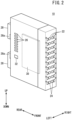
- FIG. 2 is a perspective view of the electronic device 10 of FIG. 1 .
- Each of the plurality of power connectors 24 is a connector for connecting to an external power supply.
- the plurality of power connectors 24 are provided on the front side of the electronic device 10, similarly to the plurality of inserted portions 22.
- the number of the power connectors 24 is the same as the number of individual power terminals 40 (see FIG. 3 ) described later.
- the plurality of power connectors 24 are provided at the lowest portion of the electronic device 10, but the present invention is not limited to this.
- Each of the plurality of contactors 26 is a member for electrically connecting the electronic device 10 to another unit 100 (see also FIG. 4 ).
- the other unit 100 is another electronic device (10) adjacent to the electronic device 10 in the left-right direction or a communication coupler unit (18).
- One or more contactors 26 are provided on each of the left side of the electronic device 10 and the right side of the electronic device 10. Illustration of the right side of the electronic device 10 is omitted.
- the plurality of contactors 26 constitute a transmission path for inputting and outputting signals between the electronic device 10 and the other unit 100.
- FIG. 3 is a diagram illustrating the signal processing module 30 of the electronic device 10 of FIG. 2 .
- the signal processing module 30 exemplified in the present embodiment includes a circuit board 34, a plurality of processing circuits 36, a plurality of signal output terminals 38, a plurality of individual power terminals 40, and a plurality of common power terminals 42.
- the plurality of processing circuits 36, the plurality of signal output terminals 38, the plurality of individual power terminals 40, and the plurality of common power terminals 42 are provided on the circuit board 34.
- Each of the plurality of processing circuits (communication circuits) 36 includes, for example, a driver circuit and a control integrated circuit (IC) as appropriate.
- the driver circuit outputs a signal to the device 16 by using the supplied electric power.
- the control IC controls the supply of power to the driver circuit.
- Each of the plurality of processing circuits (in particular, the control ICs) 36 processes signals input from the other unit 100 through the contactor 26 and processes signals input from the device 16 through the external terminal 16a. Descriptions on a more specific configuration of the processing circuit 36 is omitted.
- the number of the plurality of processing circuits 36 is two for illustration.
- the circuit board 34 has one surface (first surface) 34a and the other surface (second surface) 34b.
- the two processing circuits 36 are provided respectively on the first surface 34a and the second surface 34b.
- the processing circuit 36 provided on the first surface 34a is hereinafter also referred to as a first processing circuit 36A.
- the processing circuit 36 provided on the second surface 34b is hereinafter also referred to as a second processing circuit 36B.
- the plurality of signal output terminals 38 are provided to electrically connect the plurality of external terminals 16a inserted into the plurality of inserted portions 22, to the plurality of processing circuits 36.
- the number of the signal output terminals 38 is the same as the number of the inserted portions 22. However, in order to avoid complication of the drawing, the number of the signal output terminals 38 shown in FIG. 3 is "4", and the other signal output terminals 38 are not shown.
- the plurality of signal output terminals 38 are connected to the plurality of processing circuits 36.
- the number of the signal output terminals 38 connected to each processing circuit 36 is not particularly limited. The number of the signal output terminals 38 connected to each processing circuit 36 may be different. However, all the signal output terminals 38 are connected to any one of the plurality of processing circuits 36.
- the plurality of individual power terminals 40 are electrically connected respectively to the different processing circuits 36.
- the plurality of individual power terminals 40 include a first individual power terminal 40A and a second individual power terminal 40B.
- the first individual power terminal 40A is electrically connected to the first processing circuit 36A.
- the second individual power terminal 40B is electrically connected to the second processing circuit 36B.
- the conductive member 32 is attachable to and detachable from the electronic device 10.
- the conductive member 32 has electrical conductivity.
- the conductive member 32 is in contact with the first common power terminal 42A and the second common power terminal 42B. As a result, the first common power terminal 42A and the second common power terminal 42B are electrically connected to each other.
- the dashed arrows in FIG. 4 simply illustrate the flow of electric power supply.
- the other unit 100L and the conductive member 32 when the other unit 100L and the conductive member 32 are electrically connected to each other, power can be supplied from the other unit 100L to the first processing circuit 36A and the second processing circuit 36B.
- the conductive member 32 is also electrically connected to the other unit 100R. Therefore, power can be supplied also to the other unit 100R (the processing circuit of the other unit 100R) from the other unit 100L via the conductive member 32.
- power may be supplied to the first processing circuit 36A, the second processing circuit 36B, and the other unit 100L (the processing circuit of the other unit 100L) from the other unit 100R via the conductive member 32.
- power may be supplied from the electronic device 10 to the other unit 100L and the other unit 100R. That is, the plurality of individual power terminals 40, the other unit 100L, and the other unit 100R are electrically connected via the conductive member 32. One of the plurality of individual power terminals 40 is connected to a power supply via the power connector 24. Thus, power can be supplied from the power supply to the other unit 100L and the other unit 100R via the electronic device 10.
- the conductive member 32 may be removed from the electronic device 10.
- the first individual power terminal 40A is connected to a power supply.
- the first individual power terminal 40A is connected to the power supply through its own power connector 24.
- the power supply connected to the first individual power terminal 40A can supply electric power to the first processing circuit 36A.
- the second individual power terminal 40B may be connected to another power supply through its own power connector 24.
- the power supply connected to the second individual power terminal 40B can supply electric power to the second processing circuit 36B.
- the operator can easily change the number of processing circuits connected to one power supply.
- the operator can supply power from one power supply to a plurality of electronic devices 10 by attaching the conductive member 32 to the electronic device 10. This is preferable for the operator in that the number of required power supplies can be reduced. It is also preferable for the operator in that wiring of the power supply is simplified.
- the operator may remove the conductive member 32. This allows the operator to separate the plurality of processing circuits 36 into a plurality of groups.
- the plurality of processing circuits 36 receive power supply from different power supplies, for each group. Accordingly, for example, even when an abnormality occurs in one power supply, the processing circuits 36 of the groups corresponding to the power supplies other than the abnormal power supply can continue the operation. That is, the availability of the communication system 12 is secured.
- FIG. 5 is a diagram illustrating the electronic device 10 provided with the conductive member 32A (32) according to a first modification.
- the conductive member 32A is a member that is electrically connected to one of the other unit 100L and the other unit 100R and to the plurality of processing circuits 36 of the electronic device 10.
- the conductive member 32A is electrically connected to the other unit 100L and the plurality of processing circuits 36 of the electronic device 10.
- the electronic device 10 including the conductive member 32A can receive power supply from the other unit 100L.
- power may be supplied from the electronic device 10 to the other unit 100L.
- the other unit 100R is connected to a power supply different from the power supply that supplies power to the electronic device 10 and the other unit 100L.
- FIG. 6 is a diagram showing an electronic device 10 provided with a conductive member 32A according to a first modification, which is an example different from FIG. 5 .
- the electronic device 10 including the conductive member 32A can receive power supply from the other unit 100R. Power may be supplied from the electronic device 10 to the other unit 100R.
- FIG. 7 is a diagram illustrating a state in which a power supply is connected to the individual power terminals 40 of the electronic device 10 provided with the conductive member 32B (32) according to a second modification.
- the conductive member 32B is a member that is electrically connected to the plurality of processing circuits 36 (36A and 36B) of the electronic device 10 but is not electrically connected to the other units 100.
- one of the first individual power terminal 40A and the second individual power terminal 40B is connected to the power supply.
- power is supplied from the power supply to both the first individual power terminal 40A and the second individual power terminal 40B.
- each of the conductive member 32 of the embodiment, the conductive member 32A of the first modification, and the conductive member 32B of the present modification may be provided to the operator.
- FIG. 8A is a diagram illustrating an electronic device 10A (10) according to a third modification.
- FIG. 8B is an exploded view of the electronic device 10A of FIG. 8A .
- the electronic device 10A may be separable into a plurality of units.
- the electronic device 10A of the present modification can be separated into a connector unit (terminal block) 46, a base unit 48, and a signal processing unit 50.
- the connector unit 46, the signal processing unit 50, and the base unit 48 are arranged in this order in the rearward direction ( FIG. 8B ).
- the connector unit 46 is a unit including the plurality of inserted portions 22 and the plurality of power connectors 24.
- the base unit 48 is a unit including the plurality of contactors 26 and the end engagement portions 28.
- the conductive member 32 is detachably installed on the base unit 48.
- the signal processing unit 50 is a unit including the signal processing module 30.
- the base unit 48 provided with the conductive member 32 and the base unit 48 not provided with the conductive member 32 may be separately provided to the operator.
- a base unit 48 which the conductive member 32 is attachable to and detachable from may be provided to the operator. Particularly in the former case, the operator can easily change the connection mode to the power supply simply by changing the base unit 48.
- the division of the electronic device 10 is not limited to the illustration in FIG. 8A .
- the base unit 48 and the signal processing unit 50 may be integrally formed.
- the signal processing unit 50 and the connector unit 46 may be integrally provided.
- the electronic device (10) that performs input and output of a signal includes: the plurality of processing circuits (36) configured to perform input and output of the signal; the plurality of common power terminals (42) connected respectively to the different processing circuits to supply electric power to each of the plurality of processing circuits; the plurality of individual power terminals (40) connected respectively to the different processing circuits to supply electric power to each of the plurality of processing circuits; and the conductive member (32) attachably and detachably provided and configured to electrically connect the plurality of common power terminals to each other.
- Each of the plurality of individual power terminals may be a terminal configured to connect a power supply and each of the processing circuits in order to supply electric power to each of the processing circuits.
- power can be supplied to the plurality of processing circuits by connecting a power supply to the plurality of individual power terminals.
- the conductive member may be electrically connected to a first other electronic device (100L, 100R) adjacent to the electronic device in a first direction and may supply electric power supplied from the first other electronic device, to the plurality of processing circuits. With this configuration, power can be supplied from the first other electronic device to the plurality of processing circuits.
- the conductive member may be electrically connected to the second other electronic device (100R, 100L) adjacent to the electronic device in a second direction opposite to the first direction and may supply the electric power to the second other electronic device. Accordingly, by supplying power to the electronic device, electric power can be supplied to the processing circuit of the second other electronic device.
- the conductive member may supply electric power supplied from at least one of the plurality of individual power terminals, to the plurality of processing circuits. Thus, the number of necessary power supplies can be reduced.
- the conductive member may be electrically connected to another electronic device (100R, 100L) adjacent to the electronic device in a predetermined installation direction and may supply the electric power to the other electronic device.
- another electronic device 100R, 100L
- electric power can be supplied to the processing circuit of the other electronic device.
- the electronic device may further include the circuit board (34) including the first surface (34a) and the second surface (34b) and provided with the plurality of processing circuits, wherein the plurality of common power terminals may include at least one first common power terminal provided on the first surface and at least one second common power terminal provided on the second surface.
- the electronic device may be divided into: the signal processing unit (50) including the plurality of processing circuits, the plurality of common power terminals, and the plurality of individual power terminals; and the base unit (48) that is attachable to and detachable from the signal processing unit and that is configured to detachably support the conductive member. This facilitates maintenance work of the electronic device.
- the electronic device may further include the terminal block (46) configured to be connected to the device (16) serving as an input/output target of the signal, wherein the terminal block may be provided with connectors (24) configured to connect the plurality of individual power terminals to the plurality of power supplies.
- the electronic device may be an I/O unit.
Landscapes
- Engineering & Computer Science (AREA)
- Automation & Control Theory (AREA)
- Microelectronics & Electronic Packaging (AREA)
- Power Engineering (AREA)
- Theoretical Computer Science (AREA)
- Human Computer Interaction (AREA)
- Physics & Mathematics (AREA)
- General Engineering & Computer Science (AREA)
- General Physics & Mathematics (AREA)
- Power Sources (AREA)
- Programmable Controllers (AREA)
- Semiconductor Integrated Circuits (AREA)
Abstract
Description
- The present invention relates to an electronic device (electronic apparatus).
-
JP 2016-110460 A - The electronic device outputs an output signal using power supplied from a power supply. The electronic devices include a model that receives electric power supplied from one power supply (common power supply) together with other electronic devices, and a model that receives electric power supplied from different power supplies (individual power supplies) for each electronic device.
- There is a case in which the operator may want to select whether to supply electric power to a plurality of electronic devices from one power supply or to supply electric power to each electronic device from a different power supply individually, depending on the situation. However, in the conventional electronic device, there is a problem that the connection mode for the electronic device with the power supply is limited depending on the model of the electronic device, as described above.
- The present invention has the object of solving the aforementioned problems.
- According to an aspect of the present invention, there is provided an electronic device that performs input and output of a signal, including: a plurality of processing circuits configured to perform input and output of the signal; a plurality of common power terminals connected respectively to the different processing circuits to supply electric power to each of the plurality of processing circuits; a plurality of individual power terminals connected respectively to the different processing circuits to supply electric power to each of the plurality of processing circuits; and a conductive member attachably and detachably provided and configured to electrically connect the plurality of common power terminals to each other.
- According to the present invention, there is provided an electronic device capable of easily changing a connection mode to a power supply.
-
-
FIG. 1 is a diagram illustrating a communication system configured to include an electronic device according to an embodiment of the present invention; -
FIG. 2 is a perspective view of the electronic device ofFIG. 1 ; -
FIG. 3 is a diagram representing a signal processing module of the electronic device ofFIG. 2 ; -
FIG. 4 is a view showing a state in which a conductive member is attached to the signal processing module ofFIG. 3 ; -
FIG. 5 is a diagram illustrating an electronic device provided with a conductive member according to a first modification; -
FIG. 6 is a diagram illustrating an electronic device provided with a conductive member according to a first modification, which is an example different fromFIG. 5 ; -
FIG. 7 is a diagram illustrating a state in which a power supply is connected to an individual power terminal of an electronic device provided with a conductive member according to a second modification; -
FIG. 8A is a diagram illustrating an electronic device according to a third modification; and -
FIG. 8B is an exploded view of the electronic device ofFIG. 8A . -
FIG. 1 is a diagram illustrating acommunication system 12 configured to include anelectronic device 10 according to an embodiment of the present invention. Arrows inFIG. 1 indicate directions (front, rear, left, right, up, and down) used for the following descriptions. The front-rear direction, the left-right direction, and the up-down direction are orthogonal to each other. The arrows in the other figures correspond to those inFIG. 1 unless otherwise indicated. - The
communication system 12 is a system that transmits signals between acontrol device 14 and adevice 16. Thecommunication system 12 includes acommunication coupler unit 18 and a plurality ofelectronic devices 10. Thecommunication coupler unit 18 is a master unit. The plurality of electronic devices are slave units of thecommunication coupler unit 18. Theelectronic device 10 is, for example, an I/O unit (input/output unit). - The
communication coupler unit 18 is connected to thecontrol device 14. Thecontrol device 14 is an electronic device that controls a mechanical device such as a machine tool or a robot. Thecommunication coupler unit 18 further includes a connection terminal that can be connected to theelectronic device 10. The connection terminal is provided at a portion of thecommunication coupler unit 18 that is adjacent to theelectronic device 10. Note that the connection terminal of thecommunication coupler unit 18 are not shown. - Each of the plurality of
electronic devices 10 is connected to thedevice 16. Thedevice 16 is, for example, an actuator such as a switch. The actuator is provided in, for example, the machine tool or the robot. The actuator operates in response to a signal input from theelectronic device 10. In this regard, thedevice 16 includes a terminal (external terminal) 16a for connection with theelectronic device 10. Thedevice 16 may output a signal to thecontrol device 14 via theelectronic device 10. - The
communication coupler unit 18 and the plurality ofelectronic devices 10 are arranged along the left-right direction. Here, thecommunication coupler unit 18 and the plurality ofelectronic devices 10 are installed on apredetermined installation member 20. Theinstallation member 20 is, for example, a DIN rail. Theinstallation member 20 ofFIG. 1 extends along the left-right direction. Further, theinstallation member 20 is disposed behind thecommunication coupler unit 18 and the plurality ofelectronic devices 10. - The
control device 14 and the device (s) 16 are connected via thecommunication system 12. Thecontrol device 14 transmits signals to thedevice 16 via thecommunication system 12. Thecontrol device 14 also receives signals from thedevice 16 via thecommunication system 12. Each of thecommunication coupler unit 18 and theelectronic device 10 performs signal processing such that signals are appropriately transmitted and received between thecontrol device 14 and thedevice 16. Descriptions on the details of the signal processing performed by thecommunication coupler unit 18 are omitted. -
FIG. 2 is a perspective view of theelectronic device 10 ofFIG. 1 . - The
electronic device 10 preferably has a substantially flat plate shape that is thin in a direction (left-right direction) in which thecommunication coupler unit 18 and the otherelectronic devices 10 are arranged in series. Thus, thecommunication system 12 becomes compact in size. Theelectronic device 10 includes a plurality of insertedportions 22, a plurality ofpower connectors 24, a plurality ofcontactors 26,end engagement portions 28, asignal processing module 30, and a conductive member 32 (seeFIG. 2 ). - The plurality of inserted
portions 22 are provided on the front side of theelectronic device 10. The plurality ofexternal terminals 16a (seeFIG. 1 ) are inserted into the plurality of insertedportions 22. Each of the plurality of insertedportions 22 is appropriately equipped with a terminal electrically connected to the insertedexternal terminal 16a. The terminal electrically connected to theexternal terminal 16a are not shown. - Each of the plurality of
power connectors 24 is a connector for connecting to an external power supply. The plurality ofpower connectors 24 are provided on the front side of theelectronic device 10, similarly to the plurality of insertedportions 22. The number of thepower connectors 24 is the same as the number of individual power terminals 40 (seeFIG. 3 ) described later. InFIGS. 1 and2 , the plurality ofpower connectors 24 are provided at the lowest portion of theelectronic device 10, but the present invention is not limited to this. - Each of the plurality of
contactors 26 is a member for electrically connecting theelectronic device 10 to another unit 100 (see alsoFIG. 4 ). Theother unit 100 is another electronic device (10) adjacent to theelectronic device 10 in the left-right direction or a communication coupler unit (18). One ormore contactors 26 are provided on each of the left side of theelectronic device 10 and the right side of theelectronic device 10. Illustration of the right side of theelectronic device 10 is omitted. The plurality ofcontactors 26 constitute a transmission path for inputting and outputting signals between theelectronic device 10 and theother unit 100. - The
end engagement portions 28 cause theelectronic device 10 to engage with the installation member 20 (seeFIG. 1 ). Each of theend engagement portions 28 includes, for example, aclaw 28a. Theclaw 28a is engageable with theinstallation member 20. Theend engagement portions 28 are provided at a rear portion of theelectronic device 10. - The
signal processing module 30 is a module (a group of electronic components or a circuit) configured to be electrically connected to the plurality ofexternal terminals 16a and theother units 100. Thesignal processing module 30 inputs and outputs signals to and from theother unit 100 which is conducted thereto. -
FIG. 3 is a diagram illustrating thesignal processing module 30 of theelectronic device 10 ofFIG. 2 . - The
signal processing module 30 exemplified in the present embodiment includes acircuit board 34, a plurality ofprocessing circuits 36, a plurality ofsignal output terminals 38, a plurality ofindividual power terminals 40, and a plurality ofcommon power terminals 42. The plurality ofprocessing circuits 36, the plurality ofsignal output terminals 38, the plurality ofindividual power terminals 40, and the plurality ofcommon power terminals 42 are provided on thecircuit board 34. - Each of the plurality of processing circuits (communication circuits) 36 includes, for example, a driver circuit and a control integrated circuit (IC) as appropriate. The driver circuit outputs a signal to the
device 16 by using the supplied electric power. The control IC controls the supply of power to the driver circuit. Each of the plurality of processing circuits (in particular, the control ICs) 36 processes signals input from theother unit 100 through thecontactor 26 and processes signals input from thedevice 16 through theexternal terminal 16a. Descriptions on a more specific configuration of theprocessing circuit 36 is omitted. - In the present embodiment, the number of the plurality of
processing circuits 36 is two for illustration. Thecircuit board 34 has one surface (first surface) 34a and the other surface (second surface) 34b. The twoprocessing circuits 36 are provided respectively on thefirst surface 34a and thesecond surface 34b. - The
processing circuit 36 provided on thefirst surface 34a is hereinafter also referred to as afirst processing circuit 36A. Theprocessing circuit 36 provided on thesecond surface 34b is hereinafter also referred to as asecond processing circuit 36B. - The plurality of
signal output terminals 38 are provided to electrically connect the plurality ofexternal terminals 16a inserted into the plurality of insertedportions 22, to the plurality ofprocessing circuits 36. The number of thesignal output terminals 38 is the same as the number of the insertedportions 22. However, in order to avoid complication of the drawing, the number of thesignal output terminals 38 shown inFIG. 3 is "4", and the othersignal output terminals 38 are not shown. - The plurality of
signal output terminals 38 are connected to the plurality ofprocessing circuits 36. The number of thesignal output terminals 38 connected to eachprocessing circuit 36 is not particularly limited. The number of thesignal output terminals 38 connected to eachprocessing circuit 36 may be different. However, all thesignal output terminals 38 are connected to any one of the plurality ofprocessing circuits 36. - Each of the plurality of
individual power terminals 40 is, for example, an electrode pad. The plurality ofindividual power terminals 40 are provided for electrical connection with a power supply. Each of the plurality ofindividual power terminals 40 is electrically connected to the power supply through the corresponding one of thepower connectors 24 that are provided corresponding respectively to theindividual power terminals 40. - The plurality of
individual power terminals 40 are electrically connected respectively to thedifferent processing circuits 36. The plurality ofindividual power terminals 40 include a firstindividual power terminal 40A and a secondindividual power terminal 40B. The firstindividual power terminal 40A is electrically connected to thefirst processing circuit 36A. The secondindividual power terminal 40B is electrically connected to thesecond processing circuit 36B. - Each of the plurality of
common power terminals 42 is, for example, an electrode pad. The plurality ofcommon power terminals 42 are electrically connected respectively to thedifferent processing circuits 36. The plurality ofcommon power terminals 42 include a firstcommon power terminal 42A and a secondcommon power terminal 42B. The firstcommon power terminal 42A is electrically connected to thefirst processing circuit 36A. The secondcommon power terminal 42B is electrically connected to thesecond processing circuit 36B. - The first
common power terminal 42A and the firstindividual power terminal 40A are electrically connected to each other via aconductive wire 44a. Theconductive wire 44a and thefirst processing circuit 36A are electrically connected to each other via aconductive wire 44b. Further, the secondcommon power terminal 42B and the secondindividual power terminal 40B are electrically connected to each other via aconductive wire 44c. Theconductive wire 44c and thesecond processing circuit 36B are electrically connected to each other via aconductive wire 44d. -
FIG. 4 is a view showing a state in which theconductive member 32 is attached to thesignal processing module 30 ofFIG. 3 . - The
conductive member 32 is attachable to and detachable from theelectronic device 10. Theconductive member 32 has electrical conductivity. Theconductive member 32 is in contact with the firstcommon power terminal 42A and the secondcommon power terminal 42B. As a result, the firstcommon power terminal 42A and the secondcommon power terminal 42B are electrically connected to each other. - The
conductive member 32 is exposed to outside on the left side of theelectronic device 10. Accordingly, theconductive member 32 can be electrically connected to the other unit 100 (100L) installed on the left side of theelectronic device 10. Theconductive member 32 is also exposed to outside on the right side of theelectronic device 10. Accordingly, theconductive member 32 can be electrically connected to the other unit 100 (100R) installed on the right side of theelectronic device 10. Theconductive member 32 is substantially symmetrically exposed to outside on the left side of theelectronic device 10 and the right side of theelectronic device 10. However, theconductive member 32 may be asymmetrically exposed to outside on the left side of theelectronic device 10 and the right side of theelectronic device 10. - The dashed arrows in
FIG. 4 simply illustrate the flow of electric power supply. As indicated by the dashed arrows, when theother unit 100L and theconductive member 32 are electrically connected to each other, power can be supplied from theother unit 100L to thefirst processing circuit 36A and thesecond processing circuit 36B. Theconductive member 32 is also electrically connected to theother unit 100R. Therefore, power can be supplied also to theother unit 100R (the processing circuit of theother unit 100R) from theother unit 100L via theconductive member 32. Alternatively, power may be supplied to thefirst processing circuit 36A, thesecond processing circuit 36B, and theother unit 100L (the processing circuit of theother unit 100L) from theother unit 100R via theconductive member 32. - Alternatively, power may be supplied from the
electronic device 10 to theother unit 100L and theother unit 100R. That is, the plurality ofindividual power terminals 40, theother unit 100L, and theother unit 100R are electrically connected via theconductive member 32. One of the plurality ofindividual power terminals 40 is connected to a power supply via thepower connector 24. Thus, power can be supplied from the power supply to theother unit 100L and theother unit 100R via theelectronic device 10. - The
conductive member 32 may be removed from theelectronic device 10. In this case, the firstindividual power terminal 40A is connected to a power supply. The firstindividual power terminal 40A is connected to the power supply through itsown power connector 24. Thus, the power supply connected to the firstindividual power terminal 40A can supply electric power to thefirst processing circuit 36A. In addition, the secondindividual power terminal 40B may be connected to another power supply through itsown power connector 24. Thus, the power supply connected to the secondindividual power terminal 40B can supply electric power to thesecond processing circuit 36B. - According to the present embodiment, the operator can easily change the number of processing circuits connected to one power supply. The operator can supply power from one power supply to a plurality of
electronic devices 10 by attaching theconductive member 32 to theelectronic device 10. This is preferable for the operator in that the number of required power supplies can be reduced. It is also preferable for the operator in that wiring of the power supply is simplified. On the other hand, the operator may remove theconductive member 32. This allows the operator to separate the plurality ofprocessing circuits 36 into a plurality of groups. The plurality ofprocessing circuits 36 receive power supply from different power supplies, for each group. Accordingly, for example, even when an abnormality occurs in one power supply, theprocessing circuits 36 of the groups corresponding to the power supplies other than the abnormal power supply can continue the operation. That is, the availability of thecommunication system 12 is secured. - Hereinafter, some specific examples of the exemplary modifications according to the embodiment will be described. However, components already described in the embodiment are denoted by the same reference numerals as in the embodiment. In addition, differences from the embodiment will be mainly described below, and redundant description will be omitted as much as possible.
-
FIG. 5 is a diagram illustrating theelectronic device 10 provided with theconductive member 32A (32) according to a first modification. - The
conductive member 32A is a member that is electrically connected to one of theother unit 100L and theother unit 100R and to the plurality ofprocessing circuits 36 of theelectronic device 10. In the example ofFIG. 5 , theconductive member 32A is electrically connected to theother unit 100L and the plurality ofprocessing circuits 36 of theelectronic device 10. In this case, theelectronic device 10 including theconductive member 32A can receive power supply from theother unit 100L. However, power may be supplied from theelectronic device 10 to theother unit 100L. Theother unit 100R is connected to a power supply different from the power supply that supplies power to theelectronic device 10 and theother unit 100L. -
FIG. 6 is a diagram showing anelectronic device 10 provided with aconductive member 32A according to a first modification, which is an example different fromFIG. 5 . - When the
other unit 100R and the plurality ofprocessing circuits 36 of theelectronic device 10 are electrically connected to each other via theconductive member 32A, theelectronic device 10 including theconductive member 32A can receive power supply from the other unit 100R. Power may be supplied from theelectronic device 10 to theother unit 100R. -
FIG. 7 is a diagram illustrating a state in which a power supply is connected to theindividual power terminals 40 of theelectronic device 10 provided with theconductive member 32B (32) according to a second modification. - The
conductive member 32B is a member that is electrically connected to the plurality of processing circuits 36 (36A and 36B) of theelectronic device 10 but is not electrically connected to theother units 100. In this case, one of the firstindividual power terminal 40A and the secondindividual power terminal 40B is connected to the power supply. Thus, power is supplied from the power supply to both the firstindividual power terminal 40A and the secondindividual power terminal 40B. - Note that each of the
conductive member 32 of the embodiment, theconductive member 32A of the first modification, and theconductive member 32B of the present modification may be provided to the operator. -
FIG. 8A is a diagram illustrating anelectronic device 10A (10) according to a third modification.FIG. 8B is an exploded view of theelectronic device 10A ofFIG. 8A . - The
electronic device 10A may be separable into a plurality of units. Theelectronic device 10A of the present modification can be separated into a connector unit (terminal block) 46, abase unit 48, and asignal processing unit 50. Theconnector unit 46, thesignal processing unit 50, and thebase unit 48 are arranged in this order in the rearward direction (FIG. 8B ). - The
connector unit 46 is a unit including the plurality of insertedportions 22 and the plurality ofpower connectors 24. Thebase unit 48 is a unit including the plurality ofcontactors 26 and theend engagement portions 28. Theconductive member 32 is detachably installed on thebase unit 48. Thesignal processing unit 50 is a unit including thesignal processing module 30. By dividing theelectronic device 10 into the plurality of units, maintenance work of theelectronic device 10 can be easily performed. - The
base unit 48 provided with theconductive member 32 and thebase unit 48 not provided with theconductive member 32 may be separately provided to the operator. In addition, abase unit 48 which theconductive member 32 is attachable to and detachable from may be provided to the operator. Particularly in the former case, the operator can easily change the connection mode to the power supply simply by changing thebase unit 48. - The division of the
electronic device 10 is not limited to the illustration inFIG. 8A . For example, thebase unit 48 and thesignal processing unit 50 may be integrally formed. Further, thesignal processing unit 50 and theconnector unit 46 may be integrally provided. - The inventions that can be grasped from the above-described embodiment and the modifications thereof will be described below.
- The electronic device (10) that performs input and output of a signal, includes: the plurality of processing circuits (36) configured to perform input and output of the signal; the plurality of common power terminals (42) connected respectively to the different processing circuits to supply electric power to each of the plurality of processing circuits; the plurality of individual power terminals (40) connected respectively to the different processing circuits to supply electric power to each of the plurality of processing circuits; and the conductive member (32) attachably and detachably provided and configured to electrically connect the plurality of common power terminals to each other.
- With this configuration, the electronic device in which the connection mode to the power supply can be easily changed is provided.
- Each of the plurality of individual power terminals may be a terminal configured to connect a power supply and each of the processing circuits in order to supply electric power to each of the processing circuits. Thus, power can be supplied to the plurality of processing circuits by connecting a power supply to the plurality of individual power terminals.
- The conductive member may be electrically connected to a first other electronic device (100L, 100R) adjacent to the electronic device in a first direction and may supply electric power supplied from the first other electronic device, to the plurality of processing circuits. With this configuration, power can be supplied from the first other electronic device to the plurality of processing circuits.
- The conductive member may be electrically connected to the second other electronic device (100R, 100L) adjacent to the electronic device in a second direction opposite to the first direction and may supply the electric power to the second other electronic device. Accordingly, by supplying power to the electronic device, electric power can be supplied to the processing circuit of the second other electronic device.
- The conductive member may supply electric power supplied from at least one of the plurality of individual power terminals, to the plurality of processing circuits. Thus, the number of necessary power supplies can be reduced.
- The conductive member may be electrically connected to another electronic device (100R, 100L) adjacent to the electronic device in a predetermined installation direction and may supply the electric power to the other electronic device. Thus, by supplying electric power to the electronic device, electric power can be supplied to the processing circuit of the other electronic device.
- The electronic device may further include the circuit board (34) including the first surface (34a) and the second surface (34b) and provided with the plurality of processing circuits, wherein the plurality of common power terminals may include at least one first common power terminal provided on the first surface and at least one second common power terminal provided on the second surface.
- The electronic device may be divided into: the signal processing unit (50) including the plurality of processing circuits, the plurality of common power terminals, and the plurality of individual power terminals; and the base unit (48) that is attachable to and detachable from the signal processing unit and that is configured to detachably support the conductive member. This facilitates maintenance work of the electronic device.
- The electronic device may further include the terminal block (46) configured to be connected to the device (16) serving as an input/output target of the signal, wherein the terminal block may be provided with connectors (24) configured to connect the plurality of individual power terminals to the plurality of power supplies.
- The electronic device may be an I/O unit.
Claims (10)
- An electronic device (10) that performs input and output of a signal, comprising:a plurality of processing circuits (36) configured to perform input and output of the signal;a plurality of common power terminals (42) connected respectively to the different processing circuits to supply electric power to each of the plurality of processing circuits;a plurality of individual power terminals (40) connected respectively to the different processing circuits to supply electric power to each of the plurality of processing circuits; anda conductive member (32) attachably and detachably provided and configured to electrically connect the plurality of common power terminals to each other.
- The electronic device according to claim 1, wherein
each of the plurality of individual power terminals is a terminal configured to connect a power supply and each of the processing circuits in order to supply electric power to the processing circuits individually. - The electronic device according to claim 1 or 2, wherein
the conductive member is electrically connected to a first other electronic device that is adjacent to the electronic device in a first direction and supplies electric power supplied from the first other electronic device, to the plurality of processing circuits. - The electronic device according to claim 3, wherein
the conductive member is electrically connected to a second other electronic device that is adjacent to the electronic device in a second direction opposite to the first direction and supplies the electric power to the second other electronic device. - The electronic device according to claim 1 or 2, wherein
the conductive member supplies electric power supplied from at least one of the plurality of individual power terminals, to the plurality of processing circuits. - The electronic device according to claim 5, wherein
the conductive member is electrically connected to another electronic device that is adjacent to the electronic device in a predetermined installation direction and supplies the electric power to the other electronic device. - The electronic device according to any one of claims 1 to 6, further comprising a circuit board (34) including a first surface (34a) and a second surface (34b), and provided with the plurality of processing circuits,
wherein the plurality of common power terminals comprise at least one first common power terminal provided on the first surface and at least one second common power terminal provided on the second surface. - The electronic device according to any one of claims 1 to 7, wherein
the electronic device is divided into:a signal processing unit (50) including the plurality of processing circuits, the plurality of common power terminals, and the plurality of individual power terminals; anda base unit (48) that is attachable to and detachable from the signal processing unit and that is configured to attachably and detachably support the conductive member. - The electronic device according to any one of claims 1 to 8, further comprising a terminal block (46) configured to be connected to a device (16) serving as an input/output target of the signal,
wherein the terminal block is provided with connectors (24) configured to connect the plurality of individual power terminals to a plurality of power supplies. - The electronic device according to any one of claims 1 to 9, wherein
the electronic device is an I/O unit.
Applications Claiming Priority (2)
| Application Number | Priority Date | Filing Date | Title |
|---|---|---|---|
| JP2021050066 | 2021-03-24 | ||
| PCT/JP2022/010779 WO2022202392A1 (en) | 2021-03-24 | 2022-03-11 | Electronic apparatus |
Publications (2)
| Publication Number | Publication Date |
|---|---|
| EP4296805A1 true EP4296805A1 (en) | 2023-12-27 |
| EP4296805A4 EP4296805A4 (en) | 2025-04-09 |
Family
ID=83397109
Family Applications (1)
| Application Number | Title | Priority Date | Filing Date |
|---|---|---|---|
| EP22775184.9A Pending EP4296805A4 (en) | 2021-03-24 | 2022-03-11 | ELECTRONIC DEVICE |
Country Status (6)
| Country | Link |
|---|---|
| US (1) | US12471235B2 (en) |
| EP (1) | EP4296805A4 (en) |
| JP (1) | JP7549127B2 (en) |
| CN (1) | CN117083574A (en) |
| TW (1) | TW202240325A (en) |
| WO (1) | WO2022202392A1 (en) |
Families Citing this family (1)
| Publication number | Priority date | Publication date | Assignee | Title |
|---|---|---|---|---|
| EP4114156B1 (en) * | 2021-06-29 | 2025-08-06 | Abb Schweiz Ag | A terminal block unit for an input/output device of a modular process control system |
Family Cites Families (14)
| Publication number | Priority date | Publication date | Assignee | Title |
|---|---|---|---|---|
| JPS56157088A (en) | 1980-05-07 | 1981-12-04 | Mitsubishi Electric Corp | Input connection system |
| DE3024843C2 (en) * | 1980-07-01 | 1983-08-11 | Brown, Boveri & Cie Ag, 6800 Mannheim | Blade terminal |
| JPH0865918A (en) * | 1994-08-25 | 1996-03-08 | Fujitsu Ltd | Redundant power supply circuit |
| JP3763471B2 (en) | 2002-07-05 | 2006-04-05 | 三菱電機株式会社 | Programmable controller |
| US7383452B2 (en) * | 2005-04-07 | 2008-06-03 | Research In Motion Limited | Electronic device and method for initiating powering-up of a processor in the electronic device |
| US8579639B2 (en) * | 2010-08-20 | 2013-11-12 | Rockwell Automation Technologies, Inc. | Systems and methods for coupling input/output devices |
| US9055687B2 (en) * | 2010-08-20 | 2015-06-09 | Rockwell Automation Technologies, Inc. | Input/output circuits and devices having physically corresponding status indicators |
| TWI456397B (en) * | 2012-11-26 | 2014-10-11 | Quanta Comp Inc | computer system |
| JP2014228900A (en) | 2013-05-17 | 2014-12-08 | 株式会社キーエンス | Motor drive device and method for checking operation thereof |
| JP2016110460A (en) | 2014-12-08 | 2016-06-20 | 株式会社キーエンス | Programmable controller, method for controlling programmable controller and program |
| JP7036535B2 (en) | 2016-11-30 | 2022-03-15 | 株式会社シマノ | Electronic devices and control methods for electronic devices |
| JP7010860B2 (en) | 2019-02-06 | 2022-02-10 | ファナック株式会社 | Wiring structure |
| US11412632B2 (en) * | 2019-06-11 | 2022-08-09 | Rockwell Automation Asia Pacific Business Center Pte. Ltd. | Isolated power smart terminal block |
| US10742211B1 (en) * | 2019-07-31 | 2020-08-11 | Google Llc | Power sequencing in an active silicon interposer |
-
2022
- 2022-03-11 CN CN202280022993.5A patent/CN117083574A/en active Pending
- 2022-03-11 EP EP22775184.9A patent/EP4296805A4/en active Pending
- 2022-03-11 WO PCT/JP2022/010779 patent/WO2022202392A1/en not_active Ceased
- 2022-03-11 JP JP2023509010A patent/JP7549127B2/en active Active
- 2022-03-11 US US18/551,367 patent/US12471235B2/en active Active
- 2022-03-17 TW TW111109745A patent/TW202240325A/en unknown
Also Published As
| Publication number | Publication date |
|---|---|
| EP4296805A4 (en) | 2025-04-09 |
| JP7549127B2 (en) | 2024-09-10 |
| CN117083574A (en) | 2023-11-17 |
| WO2022202392A1 (en) | 2022-09-29 |
| TW202240325A (en) | 2022-10-16 |
| US12471235B2 (en) | 2025-11-11 |
| JPWO2022202392A1 (en) | 2022-09-29 |
| US20240172386A1 (en) | 2024-05-23 |
Similar Documents
| Publication | Publication Date | Title |
|---|---|---|
| US7041936B2 (en) | Method for connecting several welding devices and corresponding welding device | |
| EP2421347B1 (en) | Input/output module bus contact system and method | |
| EP1112606B1 (en) | A device for transferring electric signals | |
| CN113261396A (en) | Basic module and functional module for a switchgear cabinet system and switchgear cabinet system | |
| US8998654B2 (en) | Industrial automation technology input/output module | |
| EP3751972B1 (en) | Isolated power smart terminal block | |
| US20240172386A1 (en) | Electronic apparatus | |
| JP2006100269A (en) | Modular electrical parts of valve block | |
| EP1220434A2 (en) | Parallel power system and electronic apparatus using the power system | |
| JP2009516337A (en) | Method for monitoring a protective device arranged upstream of a switching device | |
| US20240168448A1 (en) | Master unit and communication system | |
| CN102395988A (en) | Card device and power supply method for card device | |
| JP2020030976A (en) | Harness manufacturing apparatus | |
| US11581710B2 (en) | Wiring structure | |
| US10622773B2 (en) | Safety switching apparatus for the secure switching off and/or on of at least one electrical machine | |
| EP4458610B1 (en) | Seat for an occupant of a vehicle | |
| US20200356520A1 (en) | Control device and inter-module communication method | |
| US10103599B2 (en) | Electromotive drive system electronic housing with plug connections for DC voltage supplies, field busses and digital inputs and outputs | |
| US20250286316A1 (en) | I/o unit and base unit | |
| US12572487B2 (en) | I/O unit, master unit, and communications system | |
| JP7568830B2 (en) | I/O unit and communication system | |
| EP0797134B1 (en) | I/o unit and panel board of numerical controller | |
| JP3808690B2 (en) | Multiple power connection device | |
| US20030155811A1 (en) | Remote input/output device | |
| JP2009060504A (en) | Image processing system |
Legal Events
| Date | Code | Title | Description |
|---|---|---|---|
| STAA | Information on the status of an ep patent application or granted ep patent |
Free format text: STATUS: THE INTERNATIONAL PUBLICATION HAS BEEN MADE |
|
| PUAI | Public reference made under article 153(3) epc to a published international application that has entered the european phase |
Free format text: ORIGINAL CODE: 0009012 |
|
| STAA | Information on the status of an ep patent application or granted ep patent |
Free format text: STATUS: REQUEST FOR EXAMINATION WAS MADE |
|
| 17P | Request for examination filed |
Effective date: 20230920 |
|
| AK | Designated contracting states |
Kind code of ref document: A1 Designated state(s): AL AT BE BG CH CY CZ DE DK EE ES FI FR GB GR HR HU IE IS IT LI LT LU LV MC MK MT NL NO PL PT RO RS SE SI SK SM TR |
|
| DAV | Request for validation of the european patent (deleted) | ||
| DAX | Request for extension of the european patent (deleted) | ||
| A4 | Supplementary search report drawn up and despatched |
Effective date: 20250310 |
|
| RIC1 | Information provided on ipc code assigned before grant |
Ipc: H05K 7/14 20060101ALI20250304BHEP Ipc: G06F 1/18 20060101ALI20250304BHEP Ipc: G05B 19/05 20060101AFI20250304BHEP |