EP4293734A1 - Micro led light projection chip and method for manufacturing same - Google Patents
Micro led light projection chip and method for manufacturing same Download PDFInfo
- Publication number
- EP4293734A1 EP4293734A1 EP22879668.6A EP22879668A EP4293734A1 EP 4293734 A1 EP4293734 A1 EP 4293734A1 EP 22879668 A EP22879668 A EP 22879668A EP 4293734 A1 EP4293734 A1 EP 4293734A1
- Authority
- EP
- European Patent Office
- Prior art keywords
- substrate
- chip
- lens
- light projection
- wafer
- Prior art date
- Legal status (The legal status is an assumption and is not a legal conclusion. Google has not performed a legal analysis and makes no representation as to the accuracy of the status listed.)
- Granted
Links
Images

Classifications
-
- H—ELECTRICITY
- H10—SEMICONDUCTOR DEVICES; ELECTRIC SOLID-STATE DEVICES NOT OTHERWISE PROVIDED FOR
- H10H—INORGANIC LIGHT-EMITTING SEMICONDUCTOR DEVICES HAVING POTENTIAL BARRIERS
- H10H20/00—Individual inorganic light-emitting semiconductor devices having potential barriers, e.g. light-emitting diodes [LED]
- H10H20/01—Manufacture or treatment
-
- H—ELECTRICITY
- H10—SEMICONDUCTOR DEVICES; ELECTRIC SOLID-STATE DEVICES NOT OTHERWISE PROVIDED FOR
- H10H—INORGANIC LIGHT-EMITTING SEMICONDUCTOR DEVICES HAVING POTENTIAL BARRIERS
- H10H20/00—Individual inorganic light-emitting semiconductor devices having potential barriers, e.g. light-emitting diodes [LED]
- H10H20/01—Manufacture or treatment
- H10H20/011—Manufacture or treatment of bodies, e.g. forming semiconductor layers
- H10H20/018—Bonding of wafers
-
- H—ELECTRICITY
- H10—SEMICONDUCTOR DEVICES; ELECTRIC SOLID-STATE DEVICES NOT OTHERWISE PROVIDED FOR
- H10H—INORGANIC LIGHT-EMITTING SEMICONDUCTOR DEVICES HAVING POTENTIAL BARRIERS
- H10H29/00—Integrated devices, or assemblies of multiple devices, comprising at least one light-emitting semiconductor element covered by group H10H20/00
- H10H29/01—Manufacture or treatment
- H10H29/012—Manufacture or treatment of active-matrix LED displays
-
- H—ELECTRICITY
- H10—SEMICONDUCTOR DEVICES; ELECTRIC SOLID-STATE DEVICES NOT OTHERWISE PROVIDED FOR
- H10H—INORGANIC LIGHT-EMITTING SEMICONDUCTOR DEVICES HAVING POTENTIAL BARRIERS
- H10H20/00—Individual inorganic light-emitting semiconductor devices having potential barriers, e.g. light-emitting diodes [LED]
- H10H20/80—Constructional details
- H10H20/85—Packages
-
- H—ELECTRICITY
- H10—SEMICONDUCTOR DEVICES; ELECTRIC SOLID-STATE DEVICES NOT OTHERWISE PROVIDED FOR
- H10H—INORGANIC LIGHT-EMITTING SEMICONDUCTOR DEVICES HAVING POTENTIAL BARRIERS
- H10H20/00—Individual inorganic light-emitting semiconductor devices having potential barriers, e.g. light-emitting diodes [LED]
- H10H20/80—Constructional details
- H10H20/85—Packages
- H10H20/855—Optical field-shaping means, e.g. lenses
-
- H—ELECTRICITY
- H10—SEMICONDUCTOR DEVICES; ELECTRIC SOLID-STATE DEVICES NOT OTHERWISE PROVIDED FOR
- H10H—INORGANIC LIGHT-EMITTING SEMICONDUCTOR DEVICES HAVING POTENTIAL BARRIERS
- H10H20/00—Individual inorganic light-emitting semiconductor devices having potential barriers, e.g. light-emitting diodes [LED]
- H10H20/80—Constructional details
- H10H20/85—Packages
- H10H20/857—Interconnections, e.g. lead-frames, bond wires or solder balls
-
- H—ELECTRICITY
- H10—SEMICONDUCTOR DEVICES; ELECTRIC SOLID-STATE DEVICES NOT OTHERWISE PROVIDED FOR
- H10H—INORGANIC LIGHT-EMITTING SEMICONDUCTOR DEVICES HAVING POTENTIAL BARRIERS
- H10H29/00—Integrated devices, or assemblies of multiple devices, comprising at least one light-emitting semiconductor element covered by group H10H20/00
- H10H29/01—Manufacture or treatment
- H10H29/036—Manufacture or treatment of packages
- H10H29/0363—Manufacture or treatment of packages of optical field-shaping means
-
- H—ELECTRICITY
- H10—SEMICONDUCTOR DEVICES; ELECTRIC SOLID-STATE DEVICES NOT OTHERWISE PROVIDED FOR
- H10H—INORGANIC LIGHT-EMITTING SEMICONDUCTOR DEVICES HAVING POTENTIAL BARRIERS
- H10H29/00—Integrated devices, or assemblies of multiple devices, comprising at least one light-emitting semiconductor element covered by group H10H20/00
- H10H29/30—Active-matrix LED displays
-
- H—ELECTRICITY
- H10—SEMICONDUCTOR DEVICES; ELECTRIC SOLID-STATE DEVICES NOT OTHERWISE PROVIDED FOR
- H10H—INORGANIC LIGHT-EMITTING SEMICONDUCTOR DEVICES HAVING POTENTIAL BARRIERS
- H10H29/00—Integrated devices, or assemblies of multiple devices, comprising at least one light-emitting semiconductor element covered by group H10H20/00
- H10H29/80—Constructional details
- H10H29/85—Packages
- H10H29/855—Optical field-shaping means, e.g. lenses
-
- H—ELECTRICITY
- H10—SEMICONDUCTOR DEVICES; ELECTRIC SOLID-STATE DEVICES NOT OTHERWISE PROVIDED FOR
- H10W—GENERIC PACKAGES, INTERCONNECTIONS, CONNECTORS OR OTHER CONSTRUCTIONAL DETAILS OF DEVICES COVERED BY CLASS H10
- H10W90/00—Package configurations
-
- H—ELECTRICITY
- H10—SEMICONDUCTOR DEVICES; ELECTRIC SOLID-STATE DEVICES NOT OTHERWISE PROVIDED FOR
- H10H—INORGANIC LIGHT-EMITTING SEMICONDUCTOR DEVICES HAVING POTENTIAL BARRIERS
- H10H20/00—Individual inorganic light-emitting semiconductor devices having potential barriers, e.g. light-emitting diodes [LED]
- H10H20/01—Manufacture or treatment
- H10H20/036—Manufacture or treatment of packages
- H10H20/0363—Manufacture or treatment of packages of optical field-shaping means
-
- H—ELECTRICITY
- H10—SEMICONDUCTOR DEVICES; ELECTRIC SOLID-STATE DEVICES NOT OTHERWISE PROVIDED FOR
- H10H—INORGANIC LIGHT-EMITTING SEMICONDUCTOR DEVICES HAVING POTENTIAL BARRIERS
- H10H29/00—Integrated devices, or assemblies of multiple devices, comprising at least one light-emitting semiconductor element covered by group H10H20/00
- H10H29/01—Manufacture or treatment
- H10H29/011—Manufacture or treatment of integrated devices comprising at least one light-emitting semiconductor component covered by group H10H20/00
-
- H—ELECTRICITY
- H10—SEMICONDUCTOR DEVICES; ELECTRIC SOLID-STATE DEVICES NOT OTHERWISE PROVIDED FOR
- H10H—INORGANIC LIGHT-EMITTING SEMICONDUCTOR DEVICES HAVING POTENTIAL BARRIERS
- H10H29/00—Integrated devices, or assemblies of multiple devices, comprising at least one light-emitting semiconductor element covered by group H10H20/00
- H10H29/10—Integrated devices comprising at least one light-emitting semiconductor component covered by group H10H20/00
- H10H29/14—Integrated devices comprising at least one light-emitting semiconductor component covered by group H10H20/00 comprising multiple light-emitting semiconductor components
- H10H29/142—Two-dimensional arrangements, e.g. asymmetric LED layout
Definitions
- the invention relates to the field of semiconductor electronics, and more particularly to a light projection chip for a Micro LED and a manufacturing method thereof.
- micro LED has the following three advantages: 1, high brightness; 2, long lifetime, high reliability, and high environmental resistance.
- the Micro LED is applied to the vehicle projection display.
- a single-point large-size LED is mostly used for the existing vehicle projection light sources, which has low integration, poor pixel density, large occupied volume and needs to be equipped with more optical components such as lenses.
- the technical problems to be solved by the invention are directed to provide a light projection chip for a Micro LED and a manufacturing method thereof, which can reduce the demand for an optical component of the light projection chip and improve the resolution of vehicle projection.
- a manufacturing method of a light projection chip for a Micro LED comprises the steps of:
- a light projection chip for a Micro LED comprises an integrated chip, a welding material and a driving base;
- the invention has advantageous effects in that the substrate is fabricated into the lens according to a pre-set array pattern on a side of the substrate of a wafer away from a metal electrode, so that the chip can be integrated with the lens without using an additional lens or an optical component. Furthermore, an integrated chip can be obtained by cutting the wafer. A chip with a high integration degree, a high pixel density and a small volume can be obtained by multiple sub-pixels on the integrated chip. Each pixel on the chip corresponds to the driving base, so that the effects of adjustable resolution and free pixel partitioning are achieved by the driving design.
- an embodiment of the invention provides a manufacturing method of a light projection chip for a Micro LED, including the steps of:
- the invention has advantageous effects in that the substrate is fabricated into the lens according to a pre-set array pattern on a side of the substrate of a wafer away from a metal electrode, so that the chip can be integrated with the lens without using an additional lens or an optical component. Furthermore, an integrated chip can be obtained by cutting the wafer. A chip with a high integration degree, a high pixel density and a small volume can be obtained by multiple sub-pixels on the integrated chip. Each pixel on the chip corresponds to the driving base, so that the effects of adjustable resolution and free pixel partitioning are achieved by the driving design.
- the method includes: arranging a pixel array of the chip on the wafer according to the arrangement of the driving base, and integrating a plurality of LED self-emitting pixels into the chip of the wafer according to the pre-set array pattern of the pixel array.
- the fabricating a substrate into a lens according to the pre-set array pattern on a side of the substrate of the wafer away from the metal electrode includes: grinding and polishing a side of the substrate of the wafer away from the metal electrode, and etching the substrate according to the pre-set array pattern to fabricate the substrate into the lens.
- using a substrate to make a lens enables a chip to integrate a lens instead of an additional lens or an optical component, thereby reducing redundant connection lines. Also, using a substrate to make a lens can also improve the corrosion resistance and acid-alkali resistance of the lens.
- the method further includes: depositing a silicon oxide layer on the lens, and etching the silicon oxide layer and adjusting the morphology of the lens.
- performing secondary deposition and secondary etching on the lens can adjust the morphology of the lens to a desired aspect ratio and tip angle.
- the fabricating a substrate into a lens according to the pre-set array pattern on a side of the substrate of the wafer away from the metal electrode further includes: depositing a silicon oxide layer on a side of a substrate of the wafer away from the metal electrode, etching the substrate and the silicon oxide layer according to the pre-set array pattern, and fabricating a lens based on the substrate and the silicon oxide layer.
- FIG. 2 another embodiment of the invention provides a light projection chip for a Micro LED including an integrated chip, a welding material and a driving base;
- the substrate is fabricated into the lens according to a pre-set array pattern on a side of the substrate of a wafer away from a metal electrode, so that the chip can be integrated with the lens without using an additional lens or an optical component. Furthermore, an integrated chip can be obtained by cutting the wafer. A chip with a high integration degree, a high pixel density and a small volume can be obtained by multiple sub-pixels on the integrated chip. Each pixel on the chip corresponds to the driving base, so that the effects of adjustable resolution and free pixel partitioning are achieved by the driving design.
- a silicon oxide layer is deposited on the side of the substrate away from the sub-pixel, and the side of the substrate away from the sub-pixel is a lens shape obtained by etching the substrate and the silicon oxide layer according to the pre-set array pattern.
- the lens-shaped side of the substrate away from the sub-pixel is provided with a silicon oxide layer having a lens-shaped surface.
- performing secondary deposition and secondary etching on the lens can adjust the morphology of the lens to a desired aspect ratio and tip angle.
- the lens shape has a bottom width of 10-200 um and a height of 50-500 um.
- the silicon oxide layer has a thickness of 10 to 300 ⁇ m.
- the morphology of the lens can be adjusted by depositing the silicon oxide layer, thereby improving the flexibility of lens fabrication.
- the above-mentioned light projection chip for the Micro LED and the manufacturing method thereof of the invention are suitable for use as a high-definition projection light source for a vehicle, and are described in the following specific embodiments:
- a manufacturing method of a light projection chip for a Micro LED comprises the steps of: S1, arranging a pixel array 1 of the chip on the wafer according to the arrangement of the driving base 8, and integrating a plurality of LED self-emitting pixels into the chip of the wafer according to the pre-set array pattern of the pixel array 1.
- 9 to 1 million high-brightness LED self-emitting pixels can be integrated into one chip.
- the chip volume depends on the number of pixels.
- the pixel density can reach above 1000 ppi, and the corresponding size is between 20 ⁇ m and 2cm.
- the lens 5 can be a convex lens for concentrating light or a concave lens for scattering light, and manufacturing the lens 5 includes the following three methods.
- an electrode of the integrated chip 6 is welded to a driving base 8 via a welding material 7 to obtain a light projection chip.
- This embodiment provides a specific manufacturing method of a light projection chip for a Micro LED. Amomg them, a substrate 4 is used to fabricate a lens 5. Specifically,
- Step 11 a GaN epitaxial slice grown on a sapphire substrate 4 is used by a MOCVD device as a base; pattern transfer is performed according to a designed chip pattern by using a photolithography apparatus such as a photolithography machine and a photoresist, and materials; and an N-type layer is fabricated by etching the GaN surface.
- a photolithography apparatus such as a photolithography machine and a photoresist, and materials
- an N-type layer is fabricated by etching the GaN surface.
- Step 12 a conductive layer is evaporated on the above-mentioned wafer; pattern transfer is performed according to a designed chip pattern by using a photolithography apparatus such as a photolithography machine and a photoresist, and materials; and the current spreading layer thin film on the N-type layer is removed by etching.
- a photolithography apparatus such as a photolithography machine and a photoresist, and materials
- Step 13 an aluminium oxide and silicon oxide protective layer is deposited on the above-mentioned wafer using a ALD device and a PECVD device; the pattern transfer is performed according to the designed chip pattern by using the photolithography apparatus such as a photolithography machine and a photoresist, and materials; and the protective layer is removed by etching, and the position of the metal electrode is reserved.
- the photolithography apparatus such as a photolithography machine and a photoresist, and materials
- the protective layer is removed by etching, and the position of the metal electrode is reserved.
- Step 14 gluing and photolithography are performed on the above-mentioned wafer, then a metal electrode is evaporated by means of metal evaporation, and then metal stripping is performed, leaving the metal electrode at a predetermined position.
- Step 15 referring to Fig. 2 , grinding and polishing are performed on the substrate 4 side of the above-mentioned wafer; pattern transfer is performed on the substrate 4 according to a designed microlens array pattern by using a photolithography apparatus such as a photolithography machine and a photoresist; and ICP etching is performed to produce an integrated lens 5.
- the bottom width of the lens 5 is 10-200 ⁇ m, and the height of the lens 5 is 50-300 ⁇ m.
- Step 16 the wafer is cut to form an integrated Micro LED chip with the lens 5.
- Step 17 the above-mentioned chip is welded to the driving base 8 via the welding material 7.
- the welding surface of the chip is a chip electrode. After welding, the chip electrode surface is located below and is combined with the driving base 8.
- the lens 5 is located above.
- the above-mentioned drive and chip are attached to a light projection chip mounting position 9 such as a vehicle, and the projection effect and the control of the projection pattern can be realized in a projection region 10 by the drive performing power supply and control.
- This embodiment provides a specific manufacturing method for a Micro LED light projection chip.
- a lens 5 fabricated by a substrate 4 is morphologyly adjusted. Specifically,
- Step 21 a GaN epitaxial slice grown on a sapphire substrate 4 is used by a MOCVD device as a base; pattern transfer is performed according to a designed chip pattern by using a photolithography apparatus such as a photolithography machine and a photoresist, and materials; and an N-type layer is fabricated by etching the GaN surface.
- a photolithography apparatus such as a photolithography machine and a photoresist, and materials
- an N-type layer is fabricated by etching the GaN surface.
- Step 22 a conductive layer is evaporated on the above-mentioned wafe; the conductive layer can be indium tin oxide or a NiAu alloy metal or molybdenum oxide; the pattern transfer is performed according to the designed chip pattern by using the photolithography apparatus such as a photolithography machine and a photoresist, and materials; the current spreading layer thin film on the N-type layer is removed by etching, and only the conductive layer is reserved on the P-GaN.
- the photolithography apparatus such as a photolithography machine and a photoresist, and materials
- the current spreading layer thin film on the N-type layer is removed by etching, and only the conductive layer is reserved on the P-GaN.
- Step 23 a titanium oxide and silicon oxide protective layer is deposited on the above-mentioned wafer using a DBR device and a PECVD device; the pattern transfer is performed according to the designed chip pattern by using the photolithography apparatus such as a photolithography machine and a photoresist, and materials; and a conductive through-hole is fabricated under the metal electrode by etching or corrosion, and the position of the metal electrode is reserved.
- the photolithography apparatus such as a photolithography machine and a photoresist, and materials
- a conductive through-hole is fabricated under the metal electrode by etching or corrosion, and the position of the metal electrode is reserved.
- Step 24 gluing and photolithography are performed on the above-mentioned wafer; the conductive pads 2 are fabricated by means of electron beam evaporation of metal or sputtering of metal, and then metal stripping is performed, leaving metal electrodes at predetermined positions.
- Step 25 the substrate 4 side of the wafer is ground and polished. It continues processing on the sapphire surface, and the pattern transfer is performed on the substrate 4 according to a designed microlens array pattern by using a photolithography apparatus such as a photolithography machine and a photoresist.
- a photolithography apparatus such as a photolithography machine and a photoresist.
- Step 26 according to the pattern produced in step 25, ICP etching is performed to produce an integrated lens 5.
- the bottom width of the lens 5 is 10-200 ⁇ m, and the height of the lens 5 is 50-500 ⁇ m.
- Step 27 a second deposition is continued on the surface of the above-mentioned lens 5 by using a ALD or PECVD device, the SiO2 material is deposited, and then a pattern is made by the photolithography machine using the photoresist.
- Step 28 referring to Fig. 3 , the lens 5 is subjected to a second etching that adjusts the morphology of the lens 5 to achieve the desired aspect ratio and tip angle.
- Step 29 the wafer is cut to make an integrated Micro LED chip with a lens 5; the above-mentioned chip is welded to the driving base 8 via the welding material 7; the welding surface of the chip is a chip electrode; after welding, the chip electrode surface is located below and is combined with the driving base 8.
- the above-mentioned drive and chip are attached to a light projection chip mounting position 9 such as a vehicle, and the projection effect and the control of the projection pattern can be realized in a projection region 10 by the drive performing power supply and control.
- This embodiment provides a specific manufacturing method of a light projection chip for a Micro LED.
- a lens 5 is fabricated by using a substrate 4 and a silicon oxide layer 11. Specifically,
- Step 31 a GaN epitaxial slice grown on a sapphire substrate 4 is used by a MOCVD device as a base; pattern transfer is performed according to a designed chip pattern by using a photolithography apparatus such as a photolithography machine and a photoresist, and materials; and an N-type layer is fabricated by etching the GaN surface.
- a photolithography apparatus such as a photolithography machine and a photoresist, and materials
- an N-type layer is fabricated by etching the GaN surface.
- Step 32 a conductive layer is evaporated on the above-mentioned wafe;
- the conductive layer can be indium tin oxide or a NiAu alloy metal or molybdenum oxide;
- the pattern transfer is performed according to the designed chip pattern by using the photolithography apparatus such as a photolithography machine and a photoresist, and materials;
- the current spreading layer thin film on the N-type layer is removed by etching, and only the conductive layer is reserved on the P-GaN.
- Step 33 a titanium oxide and silicon oxide protective layer is deposited on the above-mentioned wafer using a DBR device and a PECVD device; the pattern transfer is performed according to the designed chip pattern by using the photolithography apparatus such as a photolithography machine and a photoresist, and materials; and a conductive through-hole is fabricated under the metal electrode by etching or corrosion, and the position of the metal electrode is reserved.
- the photolithography apparatus such as a photolithography machine and a photoresist, and materials
- a conductive through-hole is fabricated under the metal electrode by etching or corrosion, and the position of the metal electrode is reserved.
- Step 34 gluing and photolithography are performed on the above-mentioned wafer; the conductive pads 2 are fabricated by means of electron beam evaporation of metal or sputtering of metal, and then metal stripping is performed, leaving metal electrodes at predetermined positions.
- Step 35 referring to Fig. 4 , the substrate 4 side of the wafer is ground and polished. Silicon oxide is deposited on the sapphire surface, with a thickness ranging from 10 ⁇ m to 300 ⁇ m.
- the pattern transfer is performed on the the silicon oxide film according to the designed microlens array pattern by using the photolithography apparatus such as a photolithography machine and a photoresist.
- the silicon oxide film between the two lens patterns is removed by wet etching.
- Step 36 ICP etching is performed on the above-mentioned pattern to produce an integrated lens 5.
- the bottom width of the lens 5 is 10-200 ⁇ m, and the height of the lens 5 is 50-500 ⁇ m.
- Step 37 the wafer is cut to form an integrated Micro LED chip with the lens 5.
- Step 38 the above-mentioned chip is welded to the driving base 8 via the welding material 7.
- the welding surface of the chip is a chip electrode. After welding, the chip electrode surface is located below and is combined with the driving base 8.
- the above-mentioned drive and chip are attached to a light projection chip mounting position 9 such as a vehicle, and the projection effect and the control of the projection pattern can be realized in a projection region 10 by the drive performing power supply and control.
- a light projection chip for a Micro LED comprises an integrated chip 6, a welding material 7 and a driving base 8.
- the integrated chip 6 includes a substrate 4 and a plurality of sub-pixels 3 located on the surface of the substrate 4.
- a bonding pad 2 is provided on the substrate surface at the position of each sub-pixel 3, and the bonding pad 2 is connected to a driving base 8 via a bonding material 7.
- a side of of the substrate 4 away from the ion pixel 3 is in the shape of a lens 5 etched according to a pre-set array pattern.
- a silicon oxide layer 11 with a lens-shaped surface is deposited on the lens-shaped surface of the side of the substrate 4 away from the ion pixel 3.
- a silicon oxide layer 11 is deposited on a side of the substrate 4 away from the sub-pixel 3.
- the side of the substrate 4 away from the sub-pixel 3 is a lens shape obtained by etching the substrate 4 and the silicon oxide layer 11 according to the pre-set array pattern.
- the bottom width of the lens shape is 10-200 ⁇ m
- the height of the lens shape is 50-500 ⁇ m
- the thickness of the silicon oxide layer 11 is 10-300 ⁇ m.
- a single-pixel display or a multi-pixel display is realized by a driving design to realize a resolution-adjustable and pixel free-partition light source effect.
- the invention provides a light projection chip for a Micro LED and a manufacturing method thereof.
- the invention has the following characteristics.
- the semiconductor processing is performed on a wafer.
- a projection light source is compressed to a very small range and has a very high pixel density by integrating a plurality of sub-pixels on the chip.
- the combination of driving base enables the spot size and shape formed by the projection light source to be more controllable, which can form a combination in real time by software, independent of hardware conditions.
- the gallium nitride, aluminum oxide and silicon oxide materials used in the manufacturing method of the invention are all materials having a very strong ability to environmental humidity, temperature, acid and alkali.
- the chip can be directly placed on the outer surface of a basic object such as a vehicle, without the need for other materials to protect or cover.
- the integrated matrix chip in the invention is provided with a lens.
- the chip and the lens are integrated on one substrate.
- the lens function can be customized at the chip processing stage to achieve light concentration and scattering.
- the lens can be composed of multiple components.
- a projection enhancement structure can be formed by combining two or more materials, and the shape and projection effect of the projection lens can be customized.
Landscapes
- Led Devices (AREA)
- Led Device Packages (AREA)
Abstract
Description
- The invention relates to the field of semiconductor electronics, and more particularly to a light projection chip for a Micro LED and a manufacturing method thereof.
- At present, micro LED has the following three advantages: 1, high brightness; 2, long lifetime, high reliability, and high environmental resistance. However, there is no case that the Micro LED is applied to the vehicle projection display. A single-point large-size LED is mostly used for the existing vehicle projection light sources, which has low integration, poor pixel density, large occupied volume and needs to be equipped with more optical components such as lenses.
- The technical problems to be solved by the invention are directed to provide a light projection chip for a Micro LED and a manufacturing method thereof, which can reduce the demand for an optical component of the light projection chip and improve the resolution of vehicle projection.
- In order to solve the technical problems, the technical solution provided by the invention is as follows.
- A manufacturing method of a light projection chip for a Micro LED comprises the steps of:
- successively preparing a conductive layer and a protective layer on a wafer according to a pre-set array pattern and evaporating a metal electrode;
- fabricating a substrate into a lens according to the pre-set array pattern on a side of the substrate of the wafer away from the metal electrode;
- cutting an etched wafer to obtain an integrated chip with the lens; and
- welding an electrode of the integrated chip and a driving base via a welding material to obtain a light projection chip.
- In order to solve the technical problems, the other technical solution provided by the invention is as follows.
- A light projection chip for a Micro LED comprises an integrated chip, a welding material and a driving base;
- the integrated chip comprises a substrate and a plurality of sub-pixels located on the surface of the substrate;
- a side of the substrate away from the sub-pixel is a lens shape etched according to a pre-set array pattern;
- the sub-pixels are arranged according to the pre-set array pattern, and a bonding pad is provided at the position of each sub-pixel on the substrate surface;
- the bonding pad is connected to the driving base via the bonding material;
- The invention has advantageous effects in that the substrate is fabricated into the lens according to a pre-set array pattern on a side of the substrate of a wafer away from a metal electrode, so that the chip can be integrated with the lens without using an additional lens or an optical component. Furthermore, an integrated chip can be obtained by cutting the wafer. A chip with a high integration degree, a high pixel density and a small volume can be obtained by multiple sub-pixels on the integrated chip. Each pixel on the chip corresponds to the driving base, so that the effects of adjustable resolution and free pixel partitioning are achieved by the driving design.
-
-
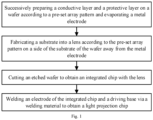
Fig. 1 is a flow chart of a manufacturing method of a light projection chip for a Micro LED in an embodiment of the invention; -
Fig. 2 is a structure diagram of a light projection chip for a Micro LED with a lens fabricated by a substrate according to an embodiment of the invention; -
Fig. 3 is a structure diagram illustrating morphology adjustment of the lens fabricated by the substrate in the light projection chip for the Micro LED according to an embodiment of the invention; -
Fig. 4 illustrates the fabrication of a lens using a substrate and a silicon oxide layer in a light projection chip for a Micro LED according to an embodiment of the invention; -
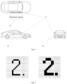
Fig. 5 is an application scene diagram of a light projection chip for a Micro LED according to an embodiment of the invention; -
Fig. 6 is a diagram showing a driving effect of a light projection chip for a Micro LED according to an embodiment of the invention; - Description of Reference Numerals:
1, pixel array; 2, bonding pad; 3, sub-pixel; 4, substrate; 5, lens; 6, integrated chip; 7, welding material; 8, driving base; 9, light projection chip mounting position; 10, projection region, 11, silicon oxide layer. - In order to explain the technical contents, achieved objects and effects of the invention in detail, it is described in combination with the detailed description and the accompanying drawings.
- With reference to
Fig. 1 , an embodiment of the invention provides a manufacturing method of a light projection chip for a Micro LED, including the steps of: - successively preparing a conductive layer and a protective layer on a wafer according to a pre-set array pattern and evaporating a metal electrode;
- fabricating a substrate into a lens according to the pre-set array pattern on a side of the substrate of the wafer away from the metal electrode;
- cutting an etched wafer to obtain an integrated chip with the lens; and
- welding an electrode of the integrated chip and a driving base via a welding material to obtain a light projection chip.
- As apparent from the above description, the invention has advantageous effects in that the substrate is fabricated into the lens according to a pre-set array pattern on a side of the substrate of a wafer away from a metal electrode, so that the chip can be integrated with the lens without using an additional lens or an optical component. Furthermore, an integrated chip can be obtained by cutting the wafer. A chip with a high integration degree, a high pixel density and a small volume can be obtained by multiple sub-pixels on the integrated chip. Each pixel on the chip corresponds to the driving base, so that the effects of adjustable resolution and free pixel partitioning are achieved by the driving design.
- Further, before the successively preparing a conductive layer and a protective layer on a wafer according to a pre-set array pattern and evaporating a metal electrode, the method includes:
arranging a pixel array of the chip on the wafer according to the arrangement of the driving base, and integrating a plurality of LED self-emitting pixels into the chip of the wafer according to the pre-set array pattern of the pixel array. - It can be seen from the above description that by directly integrating a pixel array on a wafer, it is possible to integrate a plurality of high-brightness LED self-emitting pixels into one chip, and it is possible to improve the pixel density and the degree of integration without separately soldering each chip.
- Further, the fabricating a substrate into a lens according to the pre-set array pattern on a side of the substrate of the wafer away from the metal electrode includes:
grinding and polishing a side of the substrate of the wafer away from the metal electrode, and etching the substrate according to the pre-set array pattern to fabricate the substrate into the lens. - It can be seen from the above description that using a substrate to make a lens enables a chip to integrate a lens instead of an additional lens or an optical component, thereby reducing redundant connection lines. Also, using a substrate to make a lens can also improve the corrosion resistance and acid-alkali resistance of the lens.
- Further, after the fabricating the substrate into the lens, the method further includes:
depositing a silicon oxide layer on the lens, and etching the silicon oxide layer and adjusting the morphology of the lens. - It can be seen from the above description that performing secondary deposition and secondary etching on the lens can adjust the morphology of the lens to a desired aspect ratio and tip angle.
- Furthermore, the fabricating a substrate into a lens according to the pre-set array pattern on a side of the substrate of the wafer away from the metal electrode further includes:
depositing a silicon oxide layer on a side of a substrate of the wafer away from the metal electrode, etching the substrate and the silicon oxide layer according to the pre-set array pattern, and fabricating a lens based on the substrate and the silicon oxide layer. - It can be seen from the above-mentioned description that depositing the silicon oxide layer on the substrate and performing patterned etching on the substrate and the silicon oxide layer at the same time can obtain a lens made of a composite substrate, thereby strengthening a projection structure of the chip.
- Referring to
Fig. 2 , another embodiment of the invention provides a light projection chip for a Micro LED including an integrated chip, a welding material and a driving base; - the integrated chip comprises a substrate and a plurality of sub-pixels located on the surface of the substrate;
- a side of the substrate away from the sub-pixel is a lens shape etched according to a pre-set array pattern;
- the sub-pixels are arranged according to the pre-set array pattern, and a bonding pad is provided at the position of each sub-pixel on the substrate surface;
- the bonding pad is connected to the driving base via the bonding material;
- It can be seen from the above-mentioned description that the substrate is fabricated into the lens according to a pre-set array pattern on a side of the substrate of a wafer away from a metal electrode, so that the chip can be integrated with the lens without using an additional lens or an optical component. Furthermore, an integrated chip can be obtained by cutting the wafer. A chip with a high integration degree, a high pixel density and a small volume can be obtained by multiple sub-pixels on the integrated chip. Each pixel on the chip corresponds to the driving base, so that the effects of adjustable resolution and free pixel partitioning are achieved by the driving design.
- Further, a silicon oxide layer is deposited on the side of the substrate away from the sub-pixel, and the side of the substrate away from the sub-pixel is a lens shape obtained by etching the substrate and the silicon oxide layer according to the pre-set array pattern.
- It can be seen from the above-mentioned description that depositing the silicon oxide layer on the substrate and performing patterned etching on the substrate and the silicon oxide layer at the same time can obtain a lens made of a composite substrate, thereby strengthening a projection structure of the chip.
- Further, the lens-shaped side of the substrate away from the sub-pixel is provided with a silicon oxide layer having a lens-shaped surface.
- It can be seen from the above description that performing secondary deposition and secondary etching on the lens can adjust the morphology of the lens to a desired aspect ratio and tip angle.
- Further, the lens shape has a bottom width of 10-200 um and a height of 50-500 um.
- Further, the silicon oxide layer has a thickness of 10 to 300 µm.
- It can be seen from the above description that the morphology of the lens can be adjusted by depositing the silicon oxide layer, thereby improving the flexibility of lens fabrication.
- The above-mentioned light projection chip for the Micro LED and the manufacturing method thereof of the invention are suitable for use as a high-definition projection light source for a vehicle, and are described in the following specific embodiments:
- With reference to
Fig. 1 , a manufacturing method of a light projection chip for a Micro LED comprises the steps of:
S1, arranging apixel array 1 of the chip on the wafer according to the arrangement of the drivingbase 8, and integrating a plurality of LED self-emitting pixels into the chip of the wafer according to the pre-set array pattern of thepixel array 1. - Here, 9 to 1 million high-brightness LED self-emitting pixels can be integrated into one chip. The chip volume depends on the number of pixels. The pixel density can reach above 1000 ppi, and the corresponding size is between 20 µm and 2cm.
- S2, successively preparing a conductive layer and a protective layer on a wafer according to a pre-set array pattern and evaporating a metal electrode.
- S3, fabricating a
substrate 4 into alens 5 according to the pre-set array pattern on a side of thesubstrate 4 of the wafer away from the metal electrode. - Here, the
lens 5 can be a convex lens for concentrating light or a concave lens for scattering light, and manufacturing thelens 5 includes the following three methods. - 1. Fabricating a
lens 5 using asubstrate 4
a side of thesubstrate 4 of the wafer away from the metal electrode is ground and polished, and thesubstrate 4 is etched according to a pre-set array pattern. Anintegrated lens 5 is fabricated on the basis of thesubstrate 4. - 2. Performing morphology adjustment on the
lens 5 fabricated on thesubstrate 4
A side of thesubstrate 4 of the wafer away from the metal electrode is ground and polished, and thesubstrate 4 is etched according to the pre-set array pattern to fabricate anintegrated lens 5 based on thesubstrate 4. Asilicon oxide layer 11 is deposited on theintegral lens 5, and thesilicon oxide layer 11 is etched and the morphology of thelens 5 is adjusted. - 3. Fabricating the
lens 5 using thesubstrate 4 and the silicon oxide layer 11:
Thesilicon oxide layer 11 is deposited on a side of thesubstrate 4 of the wafer away from the metal electrode. Thesubstrate 4 and thesilicon oxide layer 11 are etched according to the pre-set array pattern. Anintegrated lens 5 is fabricated on thesubstrate 4 and thesilicon oxide layer 11. - S4, cutting an etched wafer to obtain an
integrated chip 6 with thelens 5. - S5, an electrode of the
integrated chip 6 is welded to adriving base 8 via awelding material 7 to obtain a light projection chip. - This embodiment provides a specific manufacturing method of a light projection chip for a Micro LED. Amomg them, a
substrate 4 is used to fabricate alens 5. Specifically, -
Step 11, a GaN epitaxial slice grown on asapphire substrate 4 is used by a MOCVD device as a base; pattern transfer is performed according to a designed chip pattern by using a photolithography apparatus such as a photolithography machine and a photoresist, and materials; and an N-type layer is fabricated by etching the GaN surface. - Step 12, a conductive layer is evaporated on the above-mentioned wafer; pattern transfer is performed according to a designed chip pattern by using a photolithography apparatus such as a photolithography machine and a photoresist, and materials; and the current spreading layer thin film on the N-type layer is removed by etching.
- Step 13, an aluminium oxide and silicon oxide protective layer is deposited on the above-mentioned wafer using a ALD device and a PECVD device; the pattern transfer is performed according to the designed chip pattern by using the photolithography apparatus such as a photolithography machine and a photoresist, and materials; and the protective layer is removed by etching, and the position of the metal electrode is reserved.
- Step 14, gluing and photolithography are performed on the above-mentioned wafer, then a metal electrode is evaporated by means of metal evaporation, and then metal stripping is performed, leaving the metal electrode at a predetermined position.
- Step 15, referring to
Fig. 2 , grinding and polishing are performed on thesubstrate 4 side of the above-mentioned wafer; pattern transfer is performed on thesubstrate 4 according to a designed microlens array pattern by using a photolithography apparatus such as a photolithography machine and a photoresist; and ICP etching is performed to produce anintegrated lens 5. The bottom width of thelens 5 is 10-200 µm, and the height of thelens 5 is 50-300 µm. - Step 16, the wafer is cut to form an integrated Micro LED chip with the
lens 5. - Step 17, the above-mentioned chip is welded to the driving
base 8 via thewelding material 7. The welding surface of the chip is a chip electrode. After welding, the chip electrode surface is located below and is combined with the drivingbase 8. Thelens 5 is located above. - In the above-mentioned method for fabricating a Micro LED light projection chip for a vehicle, referring to
Fig. 5 , the above-mentioned drive and chip are attached to a light projectionchip mounting position 9 such as a vehicle, and the projection effect and the control of the projection pattern can be realized in aprojection region 10 by the drive performing power supply and control. - This embodiment provides a specific manufacturing method for a Micro LED light projection chip. A
lens 5 fabricated by asubstrate 4 is morphologyly adjusted. Specifically, - Step 21, a GaN epitaxial slice grown on a
sapphire substrate 4 is used by a MOCVD device as a base; pattern transfer is performed according to a designed chip pattern by using a photolithography apparatus such as a photolithography machine and a photoresist, and materials; and an N-type layer is fabricated by etching the GaN surface. - Step 22, a conductive layer is evaporated on the above-mentioned wafe; the conductive layer can be indium tin oxide or a NiAu alloy metal or molybdenum oxide; the pattern transfer is performed according to the designed chip pattern by using the photolithography apparatus such as a photolithography machine and a photoresist, and materials; the current spreading layer thin film on the N-type layer is removed by etching, and only the conductive layer is reserved on the P-GaN.
- Step 23, a titanium oxide and silicon oxide protective layer is deposited on the above-mentioned wafer using a DBR device and a PECVD device; the pattern transfer is performed according to the designed chip pattern by using the photolithography apparatus such as a photolithography machine and a photoresist, and materials; and a conductive through-hole is fabricated under the metal electrode by etching or corrosion, and the position of the metal electrode is reserved.
- Step 24, gluing and photolithography are performed on the above-mentioned wafer; the
conductive pads 2 are fabricated by means of electron beam evaporation of metal or sputtering of metal, and then metal stripping is performed, leaving metal electrodes at predetermined positions. - Step 25, the
substrate 4 side of the wafer is ground and polished. It continues processing on the sapphire surface, and the pattern transfer is performed on thesubstrate 4 according to a designed microlens array pattern by using a photolithography apparatus such as a photolithography machine and a photoresist. - Step 26, according to the pattern produced in step 25, ICP etching is performed to produce an
integrated lens 5. The bottom width of thelens 5 is 10-200 µm, and the height of thelens 5 is 50-500 µm. - Step 27, a second deposition is continued on the surface of the above-mentioned
lens 5 by using a ALD or PECVD device, the SiO2 material is deposited, and then a pattern is made by the photolithography machine using the photoresist. - Step 28, referring to
Fig. 3 , thelens 5 is subjected to a second etching that adjusts the morphology of thelens 5 to achieve the desired aspect ratio and tip angle. - Step 29, the wafer is cut to make an integrated Micro LED chip with a
lens 5; the above-mentioned chip is welded to the drivingbase 8 via thewelding material 7; the welding surface of the chip is a chip electrode; after welding, the chip electrode surface is located below and is combined with the drivingbase 8. - Referring to
Fig. 5 , the above-mentioned drive and chip are attached to a light projectionchip mounting position 9 such as a vehicle, and the projection effect and the control of the projection pattern can be realized in aprojection region 10 by the drive performing power supply and control. - This embodiment provides a specific manufacturing method of a light projection chip for a Micro LED. A
lens 5 is fabricated by using asubstrate 4 and asilicon oxide layer 11. Specifically, - Step 31, a GaN epitaxial slice grown on a
sapphire substrate 4 is used by a MOCVD device as a base; pattern transfer is performed according to a designed chip pattern by using a photolithography apparatus such as a photolithography machine and a photoresist, and materials; and an N-type layer is fabricated by etching the GaN surface. - Step 32, a conductive layer is evaporated on the above-mentioned wafe; the conductive layer can be indium tin oxide or a NiAu alloy metal or molybdenum oxide; the pattern transfer is performed according to the designed chip pattern by using the photolithography apparatus such as a photolithography machine and a photoresist, and materials; the current spreading layer thin film on the N-type layer is removed by etching, and only the conductive layer is reserved on the P-GaN.
- Step 33, a titanium oxide and silicon oxide protective layer is deposited on the above-mentioned wafer using a DBR device and a PECVD device; the pattern transfer is performed according to the designed chip pattern by using the photolithography apparatus such as a photolithography machine and a photoresist, and materials; and a conductive through-hole is fabricated under the metal electrode by etching or corrosion, and the position of the metal electrode is reserved.
- Step 34, gluing and photolithography are performed on the above-mentioned wafer; the
conductive pads 2 are fabricated by means of electron beam evaporation of metal or sputtering of metal, and then metal stripping is performed, leaving metal electrodes at predetermined positions. - Step 35, referring to
Fig. 4 , thesubstrate 4 side of the wafer is ground and polished. Silicon oxide is deposited on the sapphire surface, with a thickness ranging from 10 µm to 300 µm. The pattern transfer is performed on the the silicon oxide film according to the designed microlens array pattern by using the photolithography apparatus such as a photolithography machine and a photoresist. The silicon oxide film between the two lens patterns is removed by wet etching. - Step 36, ICP etching is performed on the above-mentioned pattern to produce an
integrated lens 5. The bottom width of thelens 5 is 10-200 µm, and the height of thelens 5 is 50-500 µm. - Step 37, the wafer is cut to form an integrated Micro LED chip with the
lens 5. - Step 38, the above-mentioned chip is welded to the driving
base 8 via thewelding material 7. The welding surface of the chip is a chip electrode. After welding, the chip electrode surface is located below and is combined with the drivingbase 8. - Referring to
Fig. 5 , the above-mentioned drive and chip are attached to a light projectionchip mounting position 9 such as a vehicle, and the projection effect and the control of the projection pattern can be realized in aprojection region 10 by the drive performing power supply and control. - Referring to
Figs. 2-6 , a light projection chip for a Micro LED comprises anintegrated chip 6, awelding material 7 and adriving base 8. - The
integrated chip 6 includes asubstrate 4 and a plurality of sub-pixels 3 located on the surface of thesubstrate 4. - A
bonding pad 2 is provided on the substrate surface at the position of each sub-pixel 3, and thebonding pad 2 is connected to adriving base 8 via abonding material 7. - With reference to
Fig. 2 , a side of of thesubstrate 4 away from the ion pixel 3 is in the shape of alens 5 etched according to a pre-set array pattern. Optionally, with reference toFig. 3 , asilicon oxide layer 11 with a lens-shaped surface is deposited on the lens-shaped surface of the side of thesubstrate 4 away from the ion pixel 3. - In another embodiment, referring to
Fig. 4 , asilicon oxide layer 11 is deposited on a side of thesubstrate 4 away from the sub-pixel 3. The side of thesubstrate 4 away from the sub-pixel 3 is a lens shape obtained by etching thesubstrate 4 and thesilicon oxide layer 11 according to the pre-set array pattern. - Here, the bottom width of the lens shape is 10-200 µm, the height of the lens shape is 50-500 µm, and the thickness of the
silicon oxide layer 11 is 10-300 µm. - The projection demonstration effect of placing a light projection chip for a Micro LED on a vehicle is shown in
Fig. 5 . With reference toFig. 6 , a single-pixel display or a multi-pixel display is realized by a driving design to realize a resolution-adjustable and pixel free-partition light source effect. - In summary, the invention provides a light projection chip for a Micro LED and a manufacturing method thereof. Compared with a conventional chip structure, the invention has the following characteristics. The semiconductor processing is performed on a wafer. A projection light source is compressed to a very small range and has a very high pixel density by integrating a plurality of sub-pixels on the chip. The combination of driving base enables the spot size and shape formed by the projection light source to be more controllable, which can form a combination in real time by software, independent of hardware conditions. The gallium nitride, aluminum oxide and silicon oxide materials used in the manufacturing method of the invention are all materials having a very strong ability to environmental humidity, temperature, acid and alkali. The chip can be directly placed on the outer surface of a basic object such as a vehicle, without the need for other materials to protect or cover. In addition, the integrated matrix chip in the invention is provided with a lens. The chip and the lens are integrated on one substrate. The lens function can be customized at the chip processing stage to achieve light concentration and scattering. The lens can be composed of multiple components. A projection enhancement structure can be formed by combining two or more materials, and the shape and projection effect of the projection lens can be customized.
- The above description is only the embodiments of the invention and do not limit the patent scope of the invention.
- Any equivalent transformations made using the content of the description and drawings of the invention, or the embodiments directly or indirectly applied in related technical fields, are also included in the scope of patent protection of the invention.
Claims (10)
- A manufacturing method of a light projection chip for a Micro LED, characterized by comprising the steps of:successively preparing a conductive layer and a protective layer on a wafer according to a pre-set array pattern and evaporating a metal electrode;fabricating a substrate into a lens according to the pre-set array pattern on a side of the substrate of the wafer away from the metal electrode;cutting an etched wafer to obtain an integrated chip with the lens; andwelding an electrode of the integrated chip and a driving base via a welding material to obtain a light projection chip.
- The manufacturing method of the light projection chip for the Micro LED according to claim 1, wherein before the successively preparing a conductive layer and a protective layer on a wafer according to a pre-set array pattern and evaporating a metal electrode, the method comprises:
arranging a pixel array of the chip on the wafer according to the arrangement of the driving base, and integrating a plurality of LED self-emitting pixels into the chip of the wafer according to the pre-set array pattern of the pixel array. - The manufacturing method of the light projection chip for the Micro LED according to claim 1, wherein the fabricating a substrate into a lens according to the pre-set array pattern on a side of the substrate of the wafer away from the metal electrode comprises:
grinding and polishing a side of the substrate of the wafer away from the metal electrode, and etching the substrate according to the pre-set array pattern to fabricate the substrate into the lens. - The manufacturing method of the light projection chip for the Micro LED according to claim 3, wherein after the fabricating the substrate into the lens, the method further comprises:
depositing a silicon oxide layer on the lens, and etching the silicon oxide layer and adjusting the morphology of the lens. - The manufacturing method of the light projection chip for the Micro LED according to claim 1, wherein the fabricating a substrate into a lens according to the pre-set array pattern on a side of the substrate of the wafer away from the metal electrode further comprises:
depositing a silicon oxide layer on a side of a substrate of the wafer away from the metal electrode, etching the substrate and the silicon oxide layer according to the pre-set array pattern, and fabricating a lens based on the substrate and the silicon oxide layer. - A light projection chip for a Micro LED, wherein the chip comprises an integrated chip, a welding material and a driving base;the integrated chip comprises a substrate and a plurality of sub-pixels located on the surface of the substrate;a side of the substrate away from the sub-pixel is a lens shape etched according to a pre-set array pattern;the sub-pixels are arranged according to the pre-set array pattern, and a bonding pad is provided at the position of each sub-pixel on the substrate surface;the bonding pad is connected to the driving base via the bonding material;
- The light projection chip for the Micro LED according to claim 6, wherein a silicon oxide layer is deposited on the side of the substrate away from the sub-pixel, and the side of the substrate away from the sub-pixel is a lens shape obtained by etching the substrate and the silicon oxide layer according to the pre-set array pattern.
- The light projection chip for the Micro LED according to claim 6, wherein the lens-shaped side of the substrate away from the sub-pixel is provided with a silicon oxide layer having a lens-shaped surface.
- The light projection chip for the Micro LED according to claim 6, wherein the lens shape has a bottom width of 10-200 um and a height of 50-500 um.
- The light projection chip for the Micro LED according to claim 7 or 8, wherein the silicon oxide layer has a thickness of 10-300 um.
Applications Claiming Priority (2)
| Application Number | Priority Date | Filing Date | Title |
|---|---|---|---|
| CN202210473461.5A CN114937731B (en) | 2022-04-29 | 2022-04-29 | Micro LED light projection chip and manufacturing method thereof |
| PCT/CN2022/097040 WO2023206713A1 (en) | 2022-04-29 | 2022-06-06 | Micro led light projection chip and method for manufacturing same |
Publications (3)
| Publication Number | Publication Date |
|---|---|
| EP4293734A1 true EP4293734A1 (en) | 2023-12-20 |
| EP4293734A4 EP4293734A4 (en) | 2024-10-23 |
| EP4293734B1 EP4293734B1 (en) | 2026-02-18 |
Family
ID=82864251
Family Applications (1)
| Application Number | Title | Priority Date | Filing Date |
|---|---|---|---|
| EP22879668.6A Active EP4293734B1 (en) | 2022-04-29 | 2022-06-06 | Micro led light projection chip and method for manufacturing same |
Country Status (4)
| Country | Link |
|---|---|
| US (1) | US12527120B2 (en) |
| EP (1) | EP4293734B1 (en) |
| CN (2) | CN114937731B (en) |
| WO (1) | WO2023206713A1 (en) |
Cited By (1)
| Publication number | Priority date | Publication date | Assignee | Title |
|---|---|---|---|---|
| US12527120B2 (en) * | 2022-04-29 | 2026-01-13 | Fujian Prima Optoelectronics Co., Ltd. | Light projection chip for micro LED and manufacturing method thereof |
Family Cites Families (33)
| Publication number | Priority date | Publication date | Assignee | Title |
|---|---|---|---|---|
| US9583678B2 (en) * | 2009-09-18 | 2017-02-28 | Soraa, Inc. | High-performance LED fabrication |
| EP3103144A1 (en) * | 2014-02-05 | 2016-12-14 | Soraa, Inc. | High-performance led fabrication |
| GB201420452D0 (en) * | 2014-11-18 | 2014-12-31 | Mled Ltd | Integrated colour led micro-display |
| CN104538514B (en) * | 2014-12-31 | 2017-07-11 | 杭州士兰微电子股份有限公司 | Flip LED chips structure and preparation method thereof |
| CN104617121A (en) * | 2015-01-04 | 2015-05-13 | 中国电子科技集团公司第五十五研究所 | Method for improving optical performance of active matrix miniature LED (light-emitting diode) display |
| US20240396288A1 (en) * | 2015-08-19 | 2024-11-28 | Kyocera Sld Laser, Inc. | Forming reflective materials on surfaces of optical elements |
| US10304811B2 (en) * | 2015-09-04 | 2019-05-28 | Hong Kong Beida Jade Bird Display Limited | Light-emitting diode display panel with micro lens array |
| CN105449056A (en) * | 2015-12-30 | 2016-03-30 | 山东浪潮华光光电子股份有限公司 | High-light-efficiency spot-evening LED chip with sapphire substrate and preparation method of LED chip |
| US9977152B2 (en) * | 2016-02-24 | 2018-05-22 | Hong Kong Beida Jade Bird Display Limited | Display panels with integrated micro lens array |
| CN106206605B (en) * | 2016-08-04 | 2019-09-03 | 上海君万微电子科技有限公司 | Flip-chip LED microdisplay array and manufacturing method thereof |
| KR20190032592A (en) * | 2016-08-08 | 2019-03-27 | 에이에스엠엘 네델란즈 비.브이. | Electronic emitter and its manufacturing method |
| CN107086260A (en) * | 2016-08-17 | 2017-08-22 | 中山大学 | A kind of flip LED chips structure and preparation method thereof |
| CN108281456B (en) * | 2018-01-19 | 2020-09-01 | 福州大学 | Micro-LED device structure and manufacturing method |
| US11784288B2 (en) * | 2018-10-26 | 2023-10-10 | Google Llc | Light-emitting diodes with integrated optical elements |
| CN109768135B (en) * | 2018-12-27 | 2020-06-19 | 武汉大学 | Full-color stacked inverted RGB Micro-LED chip array and preparation method thereof |
| US20210013367A1 (en) * | 2019-04-04 | 2021-01-14 | Bor-Jen Wu | System and Method for Making Micro LED Display |
| CN210536818U (en) * | 2019-07-05 | 2020-05-15 | 华引芯(武汉)科技有限公司 | Micro LED Micro projection device |
| US11782191B2 (en) * | 2019-10-01 | 2023-10-10 | Jade Bird Display (shanghai) Limited | Systems and fabrication methods for display panels with integrated micro-lens array |
| US11309464B2 (en) * | 2019-10-14 | 2022-04-19 | Facebook Technologies, Llc | Micro-LED design for chief ray walk-off compensation |
| CN111312068A (en) * | 2020-04-02 | 2020-06-19 | 深圳创维-Rgb电子有限公司 | Mini lamp beads, production method, backlight source and display device |
| US11322647B2 (en) * | 2020-05-01 | 2022-05-03 | Silanna UV Technologies Pte Ltd | Buried contact layer for UV emitting device |
| GB2596570B (en) * | 2020-07-01 | 2023-07-19 | Plessey Semiconductors Ltd | Light emitting array |
| CN112289899B (en) * | 2020-09-29 | 2022-04-26 | 东莞市中麒光电技术有限公司 | Micro LED wafer structure and preparation method thereof |
| CN113299678A (en) * | 2021-04-14 | 2021-08-24 | 福州大学 | Integrated packaging micro-display chip and preparation method thereof |
| CN113517265B (en) * | 2021-04-23 | 2023-06-02 | 豪威半导体(上海)有限责任公司 | Micro LED display panel and forming method thereof |
| CN113270440B (en) * | 2021-05-19 | 2022-02-25 | 福建兆元光电有限公司 | Integrated Micro LED chip and manufacturing method thereof |
| CN113314409A (en) * | 2021-05-27 | 2021-08-27 | 江苏晟驰微电子有限公司 | Manufacturing process of VBAT end low-voltage protection chip of mobile phone |
| CN113644058B (en) * | 2021-08-11 | 2022-06-28 | 福建兆元光电有限公司 | A backlight type Mini LED chip and its manufacturing method |
| CN114551656B (en) * | 2022-01-28 | 2022-11-22 | 福建兆元光电有限公司 | Manufacturing method of color Micro LED display chip module |
| CN114899182B (en) * | 2022-04-25 | 2026-01-23 | 深圳市思坦科技有限公司 | Packaging structure and method of miniature LED device and display device |
| CN114937731B (en) * | 2022-04-29 | 2023-04-07 | 福建兆元光电有限公司 | Micro LED light projection chip and manufacturing method thereof |
| CN117912376A (en) * | 2022-10-11 | 2024-04-19 | 四川启睿克科技有限公司 | Micro LED chip and projection system |
| CN115458645B (en) * | 2022-10-21 | 2023-08-11 | 福建兆元光电有限公司 | A method for manufacturing an integrated color Micro LED anti-crosstalk structure |
-
2022
- 2022-04-29 CN CN202210473461.5A patent/CN114937731B/en active Active
- 2022-04-29 CN CN202310330410.1A patent/CN116504882B/en active Active
- 2022-06-06 WO PCT/CN2022/097040 patent/WO2023206713A1/en not_active Ceased
- 2022-06-06 EP EP22879668.6A patent/EP4293734B1/en active Active
-
2023
- 2023-05-02 US US18/142,044 patent/US12527120B2/en active Active
Cited By (1)
| Publication number | Priority date | Publication date | Assignee | Title |
|---|---|---|---|---|
| US12527120B2 (en) * | 2022-04-29 | 2026-01-13 | Fujian Prima Optoelectronics Co., Ltd. | Light projection chip for micro LED and manufacturing method thereof |
Also Published As
| Publication number | Publication date |
|---|---|
| WO2023206713A1 (en) | 2023-11-02 |
| EP4293734B1 (en) | 2026-02-18 |
| CN116504882B (en) | 2025-12-05 |
| EP4293734A4 (en) | 2024-10-23 |
| CN114937731B (en) | 2023-04-07 |
| US12527120B2 (en) | 2026-01-13 |
| US20230352616A1 (en) | 2023-11-02 |
| CN116504882A (en) | 2023-07-28 |
| CN114937731A (en) | 2022-08-23 |
Similar Documents
| Publication | Publication Date | Title |
|---|---|---|
| US10643981B2 (en) | Emissive display substrate for surface mount micro-LED fluidic assembly | |
| US11410978B2 (en) | Process for fabrication of an optoelectronic device comprising a plurality of diodes | |
| US10707374B2 (en) | Etendue enhancement for light emitting diode subpixels | |
| US10734439B2 (en) | Method for producing an optoelectronic device comprising a plurality of gallium nitride diodes | |
| US10804426B2 (en) | Planar surface mount micro-LED for fluidic assembly | |
| TWI750650B (en) | Emissive display substrate for surface mount micro-led fluidic assembly and method for making same | |
| US11329188B2 (en) | Optoelectronic device manufacturing method | |
| US10998465B2 (en) | Light emitting diodes with integrated reflector for a direct view display and method of making thereof | |
| US20190280048A1 (en) | Display device and method for producing such a device | |
| CN118825173A (en) | Micro-LED display chip preparation method and Micro-LED display chip | |
| US12527120B2 (en) | Light projection chip for micro LED and manufacturing method thereof | |
| US20220238751A1 (en) | Method of manufacturing a hybrid device | |
| JP7447304B2 (en) | monolithic electronic device | |
| US20260020380A1 (en) | Light emitting diode devices with junction spacers and active metal-semiconductor contact | |
| US20260026137A1 (en) | Light emitting diode devices with extended junction spacers | |
| US11935987B2 (en) | Light emitting diode arrays with a light-emitting pixel area | |
| KR20250113990A (en) | Display including multicolor light-emitting element pixels of side-structure and method for manufacturing same | |
| JP7715327B2 (en) | Hybrid bonding with micro light-emitting diode (LED) devices | |
| WO2026094436A1 (en) | Light-emitting device and image display device | |
| CN119855311A (en) | Micro light-emitting diode chip, manufacturing method and micro light-emitting diode device | |
| CN121398308A (en) | Micro light emitting diode chip, micro light emitting diode display panel and wafer |
Legal Events
| Date | Code | Title | Description |
|---|---|---|---|
| STAA | Information on the status of an ep patent application or granted ep patent |
Free format text: STATUS: UNKNOWN |
|
| STAA | Information on the status of an ep patent application or granted ep patent |
Free format text: STATUS: THE INTERNATIONAL PUBLICATION HAS BEEN MADE |
|
| PUAI | Public reference made under article 153(3) epc to a published international application that has entered the european phase |
Free format text: ORIGINAL CODE: 0009012 |
|
| STAA | Information on the status of an ep patent application or granted ep patent |
Free format text: STATUS: REQUEST FOR EXAMINATION WAS MADE |
|
| 17P | Request for examination filed |
Effective date: 20230503 |
|
| AK | Designated contracting states |
Kind code of ref document: A1 Designated state(s): AL AT BE BG CH CY CZ DE DK EE ES FI FR GB GR HR HU IE IS IT LI LT LU LV MC MK MT NL NO PL PT RO RS SE SI SK SM TR |
|
| REG | Reference to a national code |
Ref legal event code: R079 Free format text: PREVIOUS MAIN CLASS: H01L0033580000 Ref country code: DE Ref document number: 602022030854 Country of ref document: DE Ipc: H01L0027150000 |
|
| A4 | Supplementary search report drawn up and despatched |
Effective date: 20240925 |
|
| RIC1 | Information provided on ipc code assigned before grant |
Ipc: H01L 33/44 20100101ALI20240919BHEP Ipc: H01L 33/20 20100101ALI20240919BHEP Ipc: H01L 27/15 20060101AFI20240919BHEP |
|
| DAV | Request for validation of the european patent (deleted) | ||
| DAX | Request for extension of the european patent (deleted) | ||
| REG | Reference to a national code |
Ref legal event code: R079 Free format text: PREVIOUS MAIN CLASS: H01L0027150000 Ipc: H10H0029010000 Ref country code: DE Ref document number: 602022030854 Country of ref document: DE |
|
| GRAP | Despatch of communication of intention to grant a patent |
Free format text: ORIGINAL CODE: EPIDOSNIGR1 |
|
| STAA | Information on the status of an ep patent application or granted ep patent |
Free format text: STATUS: GRANT OF PATENT IS INTENDED |
|
| RIC1 | Information provided on ipc code assigned before grant |
Ipc: H10H 29/01 20250101AFI20250905BHEP Ipc: H10H 29/30 20250101ALI20250905BHEP Ipc: H10H 29/855 20250101ALI20250905BHEP |
|
| INTG | Intention to grant announced |
Effective date: 20250929 |
|
| GRAS | Grant fee paid |
Free format text: ORIGINAL CODE: EPIDOSNIGR3 |
|
| GRAA | (expected) grant |
Free format text: ORIGINAL CODE: 0009210 |
|
| STAA | Information on the status of an ep patent application or granted ep patent |
Free format text: STATUS: THE PATENT HAS BEEN GRANTED |
|
| AK | Designated contracting states |
Kind code of ref document: B1 Designated state(s): AL AT BE BG CH CY CZ DE DK EE ES FI FR GB GR HR HU IE IS IT LI LT LU LV MC MK MT NL NO PL PT RO RS SE SI SK SM TR |
|
| REG | Reference to a national code |
Ref country code: CH Ref legal event code: F10 Free format text: ST27 STATUS EVENT CODE: U-0-0-F10-F00 (AS PROVIDED BY THE NATIONAL OFFICE) Effective date: 20260218 Ref country code: GB Ref legal event code: FG4D |
|
| REG | Reference to a national code |
Ref country code: IE Ref legal event code: FG4D |
|
| REG | Reference to a national code |
Ref country code: DE Ref legal event code: R096 Ref document number: 602022030854 Country of ref document: DE |
|
| REG | Reference to a national code |
Ref country code: CH Ref legal event code: W10 Free format text: ST27 STATUS EVENT CODE: U-0-0-W10-W00 (AS PROVIDED BY THE NATIONAL OFFICE) Effective date: 20260430 |
|
| RAP4 | Party data changed (patent owner data changed or rights of a patent transferred) |
Owner name: FUZHOU CHINA PRIMA OPTOELECTRONICS CO., LTD. |
|
| P01 | Opt-out of the competence of the unified patent court (upc) registered |
Free format text: CASE NUMBER: UPC_APP_0014326_4293734/2026 Effective date: 20260430 |
|
| REG | Reference to a national code |
Ref country code: NL Ref legal event code: MP Effective date: 20260218 |
|
| PG25 | Lapsed in a contracting state [announced via postgrant information from national office to epo] |
Ref country code: RS Free format text: LAPSE BECAUSE OF FAILURE TO SUBMIT A TRANSLATION OF THE DESCRIPTION OR TO PAY THE FEE WITHIN THE PRESCRIBED TIME-LIMIT Effective date: 20260518 |
|
| PG25 | Lapsed in a contracting state [announced via postgrant information from national office to epo] |
Ref country code: PL Free format text: LAPSE BECAUSE OF FAILURE TO SUBMIT A TRANSLATION OF THE DESCRIPTION OR TO PAY THE FEE WITHIN THE PRESCRIBED TIME-LIMIT Effective date: 20260218 |
|
| PGFP | Annual fee paid to national office [announced via postgrant information from national office to epo] |
Ref country code: GB Payment date: 20260619 Year of fee payment: 5 |
|
| PG25 | Lapsed in a contracting state [announced via postgrant information from national office to epo] |
Ref country code: GR Free format text: LAPSE BECAUSE OF FAILURE TO SUBMIT A TRANSLATION OF THE DESCRIPTION OR TO PAY THE FEE WITHIN THE PRESCRIBED TIME-LIMIT Effective date: 20260519 |
|
| REG | Reference to a national code |
Ref country code: LT Ref legal event code: MG9D |
|
| PG25 | Lapsed in a contracting state [announced via postgrant information from national office to epo] |
Ref country code: LT Free format text: LAPSE BECAUSE OF FAILURE TO SUBMIT A TRANSLATION OF THE DESCRIPTION OR TO PAY THE FEE WITHIN THE PRESCRIBED TIME-LIMIT Effective date: 20260218 |
|
| PG25 | Lapsed in a contracting state [announced via postgrant information from national office to epo] |
Ref country code: NO Free format text: LAPSE BECAUSE OF FAILURE TO SUBMIT A TRANSLATION OF THE DESCRIPTION OR TO PAY THE FEE WITHIN THE PRESCRIBED TIME-LIMIT Effective date: 20260518 |
|
| PG25 | Lapsed in a contracting state [announced via postgrant information from national office to epo] |
Ref country code: FI Free format text: LAPSE BECAUSE OF FAILURE TO SUBMIT A TRANSLATION OF THE DESCRIPTION OR TO PAY THE FEE WITHIN THE PRESCRIBED TIME-LIMIT Effective date: 20260218 Ref country code: SE Free format text: LAPSE BECAUSE OF FAILURE TO SUBMIT A TRANSLATION OF THE DESCRIPTION OR TO PAY THE FEE WITHIN THE PRESCRIBED TIME-LIMIT Effective date: 20260218 Ref country code: AT Free format text: LAPSE BECAUSE OF FAILURE TO SUBMIT A TRANSLATION OF THE DESCRIPTION OR TO PAY THE FEE WITHIN THE PRESCRIBED TIME-LIMIT Effective date: 20260218 |
|
| REG | Reference to a national code |
Ref country code: AT Ref legal event code: MK05 Ref document number: 1889689 Country of ref document: AT Kind code of ref document: T Effective date: 20260218 |
|
| PG25 | Lapsed in a contracting state [announced via postgrant information from national office to epo] |
Ref country code: HR Free format text: LAPSE BECAUSE OF FAILURE TO SUBMIT A TRANSLATION OF THE DESCRIPTION OR TO PAY THE FEE WITHIN THE PRESCRIBED TIME-LIMIT Effective date: 20260218 |
|
| PG25 | Lapsed in a contracting state [announced via postgrant information from national office to epo] |
Ref country code: IS Free format text: LAPSE BECAUSE OF FAILURE TO SUBMIT A TRANSLATION OF THE DESCRIPTION OR TO PAY THE FEE WITHIN THE PRESCRIBED TIME-LIMIT Effective date: 20260618 Ref country code: PT Free format text: LAPSE BECAUSE OF FAILURE TO SUBMIT A TRANSLATION OF THE DESCRIPTION OR TO PAY THE FEE WITHIN THE PRESCRIBED TIME-LIMIT Effective date: 20260618 |
|
| PG25 | Lapsed in a contracting state [announced via postgrant information from national office to epo] |
Ref country code: NL Free format text: LAPSE BECAUSE OF FAILURE TO SUBMIT A TRANSLATION OF THE DESCRIPTION OR TO PAY THE FEE WITHIN THE PRESCRIBED TIME-LIMIT Effective date: 20260218 |
|
| PGFP | Annual fee paid to national office [announced via postgrant information from national office to epo] |
Ref country code: FR Payment date: 20260619 Year of fee payment: 5 |
|
| PG25 | Lapsed in a contracting state [announced via postgrant information from national office to epo] |
Ref country code: LV Free format text: LAPSE BECAUSE OF FAILURE TO SUBMIT A TRANSLATION OF THE DESCRIPTION OR TO PAY THE FEE WITHIN THE PRESCRIBED TIME-LIMIT Effective date: 20260218 |
|
| PG25 | Lapsed in a contracting state [announced via postgrant information from national office to epo] |
Ref country code: BG Free format text: LAPSE BECAUSE OF FAILURE TO SUBMIT A TRANSLATION OF THE DESCRIPTION OR TO PAY THE FEE WITHIN THE PRESCRIBED TIME-LIMIT Effective date: 20260218 |