EP4290772A1 - Low power clock buffer architecture - Google Patents
Low power clock buffer architecture Download PDFInfo
- Publication number
- EP4290772A1 EP4290772A1 EP23177109.8A EP23177109A EP4290772A1 EP 4290772 A1 EP4290772 A1 EP 4290772A1 EP 23177109 A EP23177109 A EP 23177109A EP 4290772 A1 EP4290772 A1 EP 4290772A1
- Authority
- EP
- European Patent Office
- Prior art keywords
- node
- type transistor
- clock buffer
- coupled
- output signal
- Prior art date
- Legal status (The legal status is an assumption and is not a legal conclusion. Google has not performed a legal analysis and makes no representation as to the accuracy of the status listed.)
- Withdrawn
Links
Images
Classifications
-
- H—ELECTRICITY
- H03—ELECTRONIC CIRCUITRY
- H03K—PULSE TECHNIQUE
- H03K19/00—Logic circuits, i.e. having at least two inputs acting on one output; Inverting circuits
- H03K19/0008—Arrangements for reducing power consumption
- H03K19/0016—Arrangements for reducing power consumption by using a control or a clock signal, e.g. in order to apply power supply
-
- H—ELECTRICITY
- H03—ELECTRONIC CIRCUITRY
- H03K—PULSE TECHNIQUE
- H03K3/00—Circuits for generating electric pulses; Monostable, bistable or multistable circuits
- H03K3/02—Generators characterised by the type of circuit or by the means used for producing pulses
- H03K3/353—Generators characterised by the type of circuit or by the means used for producing pulses by the use, as active elements, of field-effect transistors with internal or external positive feedback
- H03K3/356—Bistable circuits
- H03K3/3565—Bistables with hysteresis, e.g. Schmitt trigger
-
- H—ELECTRICITY
- H03—ELECTRONIC CIRCUITRY
- H03K—PULSE TECHNIQUE
- H03K19/00—Logic circuits, i.e. having at least two inputs acting on one output; Inverting circuits
- H03K19/0175—Coupling arrangements; Interface arrangements
- H03K19/0185—Coupling arrangements; Interface arrangements using field effect transistors only
- H03K19/018507—Interface arrangements
- H03K19/018514—Interface arrangements with at least one differential stage
-
- H—ELECTRICITY
- H03—ELECTRONIC CIRCUITRY
- H03K—PULSE TECHNIQUE
- H03K19/00—Logic circuits, i.e. having at least two inputs acting on one output; Inverting circuits
- H03K19/02—Logic circuits, i.e. having at least two inputs acting on one output; Inverting circuits using specified components
- H03K19/08—Logic circuits, i.e. having at least two inputs acting on one output; Inverting circuits using specified components using semiconductor devices
- H03K19/094—Logic circuits, i.e. having at least two inputs acting on one output; Inverting circuits using specified components using semiconductor devices using field-effect transistors
- H03K19/0944—Logic circuits, i.e. having at least two inputs acting on one output; Inverting circuits using specified components using semiconductor devices using field-effect transistors using MOSFET or insulated gate field-effect transistors, i.e. IGFET
Definitions
- a Schmitt trigger is a comparator circuit with hysteresis implemented by applying positive feedback to the noninverting input of a comparator or differential amplifier.
- a Schmitt trigger window also becomes smaller, and the circuit will suffer a noise rejection ability issue.
- a clock buffer receives an input signal at a first node and generates an output signal at a second node.
- the clock buffer comprises a P-type transistor, a first N-type transistor, a resistor, a transistor and a switch.
- a source electrode, a gate electrode and a drain electrode of the P-type transistor are coupled to a supply voltage, the first node, and the second node, respectively.
- a gate electrode, a drain electrode and a source electrode of the first N-type transistor are coupled to the first node, the second node and a third node, respectively.
- the resistor is coupled between the first node and the second node.
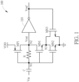
- FIG. 1 is a clock buffer 100 according to one embodiment of the present invention.
- the clock buffer 100 comprises a capacitor C, an inverter comprising aa P-type transistor MP1 and an N-type transistor MN1, a resistor R, an N-type transistor MN2, a switch (in this embodiment, an N-type transistor MN3 serves as the switch) and an inverter 110.
- the resistor R1 is coupled between the node N1 and the node N2.
- An input signal (clock signal) Vin is inputted into the node N1 via a capacitor C, the inverter comprising the P-type transistor MP1 and the N-type transistor MN1 receives the input signal Vin from the node N1 to generate an output signal (clock signal) Vout at the node N2.
- the inverter 110 receives the output signal Vout to generate an inverted output signal Vout' to control the N-type transistor MN3.
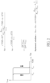
- FIG. 2 which shows a relationship between the input signal Vin and the output signal Vout and a hysteresis window (Schmitt trigger window) of the clock buffer 100 according to one embodiment of the present invention.
- the output signal Vout when the input signal Vin is higher than a first threshold voltage Vin+, the output signal Vout has a low voltage level; when the input signal Vin is below a second threshold voltage Vin-, the output signal Vout has a high voltage level; and when the input signal Vin is between the first threshold voltage Vin+ and the second threshold voltage Vin-, the output signal Vout retains its level.
- ( W / L ) MN 1 is a size of the N-type transistor MN1 (i.e. a ratio between a channel width and a channel length)
- ( W / L ) MP 1 is a size of the P-type transistor MP1 (i.e. a ratio between a channel width and a channel length).
- the N-type transistors MN1 and MN2 are the same type of transistors, if the actual equivalent resistance RMN2 the transistor N-type transistor MN2 is about 10% more than the design value, the actual equivalent resistance RMN1 the transistor N-type transistor MN1 should also be about 10% more than the design value, so "R MN2 / (R MN1 +R MN2 )" will not change too much due to the PVT variation, and the clock buffer 100 has a stable and predictable hysteresis window.
- the capacitor C serves as a DC blocking circuit to block the DC voltage of the input signal Vin.
- the capacitor C can be replaced by any other suitable DC blocking circuit.
- the capacitor C can be removed from the clock buffer 100 shown in FIG. 1 .
- the inverter 110 is configured to receive the output signal Vout to generate the inverted output signal Vout' with a full swing (i.e. from supply voltage VDD to ground voltage).
- the inverter 110 can be removed from the clock buffer 100, and the N-type transistor MN3 can be directly controlled by the output signal Vout, and the N-type transistor MN3 is replaced by another type of switch for selectively connecting the node N3 to the ground voltage when the output signal Vout has a low voltage level, and disconnecting the node N3 from the ground voltage when the output signal Vout has a high voltage level.
- the clock buffer 100 by designing the transistor MN2 coupled between the N-type transistor MN1 and the ground voltage, the clock buffer 100 has a stable and predictable hysteresis window even if suffering worse process-voltage-temperature corner. Therefore, the clock buffer 100 has a stable and predictable hysteresis window, and the phases noise is reduced.
Landscapes
- Engineering & Computer Science (AREA)
- Computer Hardware Design (AREA)
- Physics & Mathematics (AREA)
- Computing Systems (AREA)
- General Engineering & Computer Science (AREA)
- Mathematical Physics (AREA)
- Power Engineering (AREA)
- Manipulation Of Pulses (AREA)
- Logic Circuits (AREA)
Abstract
The present invention provides a clock buffer (100), wherein the clock buffer receives an input signal (Vin) at a first node (N1) and generate an output signal (Vout) at a second node (N2). The clock buffer includes a P-type transistor (MP1), a first N-type transistor (Mn1), a resistor (R), a transistor (MN2) and a switch (MN3). A source electrode, a gate electrode and a drain electrode of the P-type transistor (MP1) are coupled to a supply voltage (Vdd), the first node (N1), and the second node (Vout), respectively. A gate electrode, a drain electrode and a source electrode of the first N-type transistor (MN1) are coupled to the first node (N1), the second node (N2) and a third node (n3), respectively. The resistor (R) is coupled between the first node and the second node. The transistor (MN2) is coupled between the first N-type transistor and a ground voltage. The switch (MN3) is configured to selectively connect the third node to the ground voltage.
Description
- This application claims the benefit of
U.S. Provisional Application No. 63/349,176, filed on June 6th, 2022 - A Schmitt trigger is a comparator circuit with hysteresis implemented by applying positive feedback to the noninverting input of a comparator or differential amplifier. However, since a supply voltage of the current chip is getting lower with the demand for power saving, a Schmitt trigger window also becomes smaller, and the circuit will suffer a noise rejection ability issue.
- It is therefore an objective of the present invention to provide a clock buffer with hysteresis, which has a stable hysteresis window (Schmitt trigger window), to solve the above-mentioned problems.
- According to one embodiment of the present invention, a clock buffer is disclosed, wherein the clock buffer receives an input signal at a first node and generates an output signal at a second node. The clock buffer comprises a P-type transistor, a first N-type transistor, a resistor, a transistor and a switch. A source electrode, a gate electrode and a drain electrode of the P-type transistor are coupled to a supply voltage, the first node, and the second node, respectively. A gate electrode, a drain electrode and a source electrode of the first N-type transistor are coupled to the first node, the second node and a third node, respectively. The resistor is coupled between the first node and the second node. The transistor is coupled between the first N-type transistor and a ground voltage, wherein a gate electrode of the transistor is coupled to the node N1. The switch is configured to selectively connect the third node to the ground voltage, or disconnect the third node from the ground voltage according to the output signal.
- These and other objectives of the present invention will no doubt become obvious to those of ordinary skill in the art after reading the following detailed description of the preferred embodiment that is illustrated in the various figures and drawings.
-
-
FIG. 1 is a clock buffer according to one embodiment of the present invention. -
FIG. 2 shows a relationship between an input signal and an output signal and a hysteresis window of the clock buffer according to one embodiment of the present invention. - Certain terms are used throughout the following description and claims to refer to particular system components. As one skilled in the art will appreciate, manufacturers may refer to a component by different names. This document does not intend to distinguish between components that differ in name but not function. In the following discussion and in the claims, the terms "including" and "comprising" are used in an open-ended fashion, and thus should be interpreted to mean "including, but not limited to ...". The terms "couple" and "couples" are intended to mean either an indirect or a direct electrical connection. Thus, if a first device couples to a second device, that connection may be through a direct electrical connection, or through an indirect electrical connection via other devices and connections.
-
FIG. 1 is aclock buffer 100 according to one embodiment of the present invention. As shown inFIG. 1 , theclock buffer 100 comprises a capacitor C, an inverter comprising aa P-type transistor MP1 and an N-type transistor MN1, a resistor R, an N-type transistor MN2, a switch (in this embodiment, an N-type transistor MN3 serves as the switch) and aninverter 110. - In the
clock buffer 100, a source electrode of the P-type transistor MP1 is coupled to a supply voltage VDD, and a gate electrode and a drain electrode of the P-type transistor are coupled to a node N1 and a node N2, respectively. A gate electrode, a drain electrode and a source electrode of the N-type transistor MN1 are coupled to the node N1, the node N2 and a node N3, respectively. A gate electrode, a drain electrode and a source electrode of the N-type transistor MN2 are coupled to the node N1, the node N3 and a ground voltage, respectively. A drain electrode and a source electrode of the N-type transistor MN3 are coupled to the node N3 and the ground voltage. The resistor R1 is coupled between the node N1 and the node N2. An input signal (clock signal) Vin is inputted into the node N1 via a capacitor C, the inverter comprising the P-type transistor MP1 and the N-type transistor MN1 receives the input signal Vin from the node N1 to generate an output signal (clock signal) Vout at the node N2. Theinverter 110 receives the output signal Vout to generate an inverted output signal Vout' to control the N-type transistor MN3. - Refer to
FIG. 2 , which shows a relationship between the input signal Vin and the output signal Vout and a hysteresis window (Schmitt trigger window) of theclock buffer 100 according to one embodiment of the present invention. As shown inFIG. 2 , when the input signal Vin is higher than a first threshold voltage Vin+, the output signal Vout has a low voltage level; when the input signal Vin is below a second threshold voltage Vin-, the output signal Vout has a high voltage level; and when the input signal Vin is between the first threshold voltage Vin+ and the second threshold voltage Vin-, the output signal Vout retains its level. In the circuit structure shown inFIG. 1 , assuming that the P-type transistor and the N-type transistor have the same mobility and threshold voltage, the first threshold voltage Vin+ and the second threshold voltage Vin- can be obtained by using the following formula:

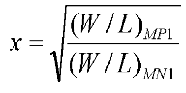
FIG. 1 , (W/L) MN1 is a size of the N-type transistor MN1 (i.e. a ratio between a channel width and a channel length), and (W/L) MP1 is a size of the P-type transistor MP1 (i.e. a ratio between a channel width and a channel length). - The hysteresis window is a difference between the first threshold voltage Vin+ and the second threshold voltage Vin-, so the hysteresis window can be represented as the following formula:

- In the formula (3), because "RMN2/ (RMN1+RMN2) " are relatively unaffected by process-voltage-temperature (PVT) variation, the hysteresis window of the
clock buffer 100 is robust to the PVT variation. For example, because the N-type transistors MN1 and MN2 are the same type of transistors, if the actual equivalent resistance RMN2 the transistor N-type transistor MN2 is about 10% more than the design value, the actual equivalent resistance RMN1 the transistor N-type transistor MN1 should also be about 10% more than the design value, so "RMN2/ (RMN1+RMN2)" will not change too much due to the PVT variation, and theclock buffer 100 has a stable and predictable hysteresis window. - In the embodiment shown in
FIG. 1 , because a DC voltage of the input signal Vin may worsen the operations of the following circuits, so the capacitor C serves as a DC blocking circuit to block the DC voltage of the input signal Vin. In another embodiment, the capacitor C can be replaced by any other suitable DC blocking circuit. In yet another embodiment, if the DC voltage of the input signal Vin will not affect the operation of theclock buffer 100, the capacitor C can be removed from theclock buffer 100 shown inFIG. 1 . - In addition, because the output signal Vout may not have a full swing, the
inverter 110 is configured to receive the output signal Vout to generate the inverted output signal Vout' with a full swing (i.e. from supply voltage VDD to ground voltage). In another embodiment, theinverter 110 can be removed from theclock buffer 100, and the N-type transistor MN3 can be directly controlled by the output signal Vout, and the N-type transistor MN3 is replaced by another type of switch for selectively connecting the node N3 to the ground voltage when the output signal Vout has a low voltage level, and disconnecting the node N3 from the ground voltage when the output signal Vout has a high voltage level. - Briefly summarized, in the clock buffer of the present invention, by designing the transistor MN2 coupled between the N-type transistor MN1 and the ground voltage, the
clock buffer 100 has a stable and predictable hysteresis window even if suffering worse process-voltage-temperature corner. Therefore, theclock buffer 100 has a stable and predictable hysteresis window, and the phases noise is reduced. - Those skilled in the art will readily observe that numerous modifications and alterations of the device and method may be made while retaining the teachings of the invention. Accordingly, the above disclosure should be construed as limited only by the metes and bounds of the appended claims.
Claims (8)
- A clock buffer (100), wherein the clock buffer (100) receives an input signal at a first node and generates an output signal at a second node, and the clock buffer (100) comprises:a P-type transistor, wherein a source electrode, a gate electrode and a drain electrode of the P-type transistor are coupled to a supply voltage, the first node, and the second node, respectively;a first N-type transistor, wherein a gate electrode, a drain electrode and a source electrode of the first N-type transistor are coupled to the first node, the second node and a third node, respectively;a resistor, coupled between the first node and the second node;a transistor, coupled between the first N-type transistor and a ground voltage, wherein a gate electrode of the transistor is coupled to the node N1; anda switch, configured to selectively connect the third node to the ground voltage, or disconnect the third node from the ground voltage according to the output signal.
- The clock buffer (100) of claim 1, wherein the transistor is a second N-type transistor, and a drain electrode and a source electrode of the second N-type transistor is coupled to the third node and the ground voltage, respectively.
- The clock buffer (100) of claim 1, wherein the switch is a third N-type transistor, and a drain electrode and a source electrode of the third N-type transistor is coupled to the third node and the ground voltage, respectively.
- The clock buffer (100) of claim 3, wherein a gate electrode of the third N-type transistor receives the output signal to connect the third node to the ground voltage, or disconnect the third node from the ground voltage according to the output signal.
- The clock buffer (100) of claim 1, further comprising:
a DC blocking circuit, wherein the input signal is inputted to the first node via the DC block circuit. - The clock buffer (100) of claim 5, wherein the DC blocking circuit is a capacitor.
- The clock buffer (100) of claim 1, further comprising:an inverter (110), coupled to second node, configured to receive the output signal to generate an inverted output signal;wherein the switch is configured to selectively connect the third node to the ground voltage, or disconnect the third node from the ground voltage according to the inverted output signal.
- The clock buffer (100) of claim 7, wherein the switch is a third N-type transistor, a gate electrode of the third N-type transistor receives the inverted output signal, and a drain electrode and a source electrode of the third N-type transistor is coupled to the third node and the ground voltage, respectively.
Applications Claiming Priority (2)
| Application Number | Priority Date | Filing Date | Title |
|---|---|---|---|
| US202263349176P | 2022-06-06 | 2022-06-06 | |
| US18/204,374 US20230396250A1 (en) | 2022-06-06 | 2023-05-31 | Low power clock buffer architecture |
Publications (1)
| Publication Number | Publication Date |
|---|---|
| EP4290772A1 true EP4290772A1 (en) | 2023-12-13 |
Family
ID=86688462
Family Applications (1)
| Application Number | Title | Priority Date | Filing Date |
|---|---|---|---|
| EP23177109.8A Withdrawn EP4290772A1 (en) | 2022-06-06 | 2023-06-02 | Low power clock buffer architecture |
Country Status (3)
| Country | Link |
|---|---|
| US (1) | US20230396250A1 (en) |
| EP (1) | EP4290772A1 (en) |
| TW (1) | TW202349873A (en) |
Families Citing this family (1)
| Publication number | Priority date | Publication date | Assignee | Title |
|---|---|---|---|---|
| TWI841911B (en) * | 2022-01-28 | 2024-05-11 | 瑞昱半導體股份有限公司 | Circuit for sar adc |
Citations (2)
| Publication number | Priority date | Publication date | Assignee | Title |
|---|---|---|---|---|
| CN108667440A (en) * | 2017-03-28 | 2018-10-16 | 峰岹科技(深圳)有限公司 | A kind of Schmitt trigger circuit |
| WO2020006990A1 (en) * | 2018-07-06 | 2020-01-09 | Shenzhen GOODIX Technology Co., Ltd. | Stacked power amplifiers using core devices |
Family Cites Families (1)
| Publication number | Priority date | Publication date | Assignee | Title |
|---|---|---|---|---|
| KR100487947B1 (en) * | 2002-11-22 | 2005-05-06 | 삼성전자주식회사 | Clock squarer |
-
2023
- 2023-05-31 US US18/204,374 patent/US20230396250A1/en not_active Abandoned
- 2023-06-02 EP EP23177109.8A patent/EP4290772A1/en not_active Withdrawn
- 2023-06-05 TW TW112120811A patent/TW202349873A/en unknown
Patent Citations (2)
| Publication number | Priority date | Publication date | Assignee | Title |
|---|---|---|---|---|
| CN108667440A (en) * | 2017-03-28 | 2018-10-16 | 峰岹科技(深圳)有限公司 | A kind of Schmitt trigger circuit |
| WO2020006990A1 (en) * | 2018-07-06 | 2020-01-09 | Shenzhen GOODIX Technology Co., Ltd. | Stacked power amplifiers using core devices |
Non-Patent Citations (1)
| Title |
|---|
| DEHLAGHI BEHZAD ET AL: "A 0.3 pJ/bit 20 Gb/s/Wire Parallel Interface for Die-to-Die Communication", IEEE JOURNAL OF SOLID-STATE CIRCUITS, IEEE, USA, vol. 51, no. 11, 1 November 2016 (2016-11-01), pages 2690 - 2701, XP011626617, ISSN: 0018-9200, [retrieved on 20161024], DOI: 10.1109/JSSC.2016.2596773 * |
Also Published As
| Publication number | Publication date |
|---|---|
| TW202349873A (en) | 2023-12-16 |
| US20230396250A1 (en) | 2023-12-07 |
Similar Documents
| Publication | Publication Date | Title |
|---|---|---|
| KR100991699B1 (en) | Constant voltage circuit and its operation control method | |
| US7521971B2 (en) | Buffer circuit | |
| US20100007420A1 (en) | Operational amplifier | |
| EP0193901B1 (en) | Comparator circuit having improved output characteristics | |
| CN104167999A (en) | Error amplifier used for switching power supply | |
| US8314638B2 (en) | Comparator circuit | |
| US6924702B2 (en) | Low supply voltage and self-biased high speed receiver | |
| EP1435693B1 (en) | Amplification circuit | |
| US20230396250A1 (en) | Low power clock buffer architecture | |
| US7830207B2 (en) | Amplifier circuit | |
| US20090289685A1 (en) | Bias voltage generation for capacitor-coupled level shifter with supply voltage tracking and compensation for input duty-cycle variation | |
| US8159303B2 (en) | Operational amplifier | |
| US7498851B2 (en) | High speed comparator | |
| CN103956983B (en) | An Error Amplifier with Clamping Function | |
| US20090115524A1 (en) | Output stage circuit and operational amplifier thereof | |
| US10212006B2 (en) | Feed-forward filtering device and associated method | |
| CN101471634B (en) | Output stage circuit and operational amplifier using it | |
| EP3282581B1 (en) | Buffer stage and control circuit | |
| US20020067213A1 (en) | Cascode amplifying circuit and folded cascode amplifying circuit | |
| CN119727672A (en) | A hysteresis comparator circuit and system | |
| US7629846B2 (en) | Source follower circuit and semiconductor apparatus | |
| CN117200758A (en) | Clock buffer | |
| CN106484016A (en) | Voltage turnover type zero compensation circuit | |
| US9337789B2 (en) | Differential receiver | |
| US11082018B2 (en) | Circuit employing MOSFETs and corresponding method |
Legal Events
| Date | Code | Title | Description |
|---|---|---|---|
| PUAI | Public reference made under article 153(3) epc to a published international application that has entered the european phase |
Free format text: ORIGINAL CODE: 0009012 |
|
| STAA | Information on the status of an ep patent application or granted ep patent |
Free format text: STATUS: THE APPLICATION HAS BEEN PUBLISHED |
|
| AK | Designated contracting states |
Kind code of ref document: A1 Designated state(s): AL AT BE BG CH CY CZ DE DK EE ES FI FR GB GR HR HU IE IS IT LI LT LU LV MC ME MK MT NL NO PL PT RO RS SE SI SK SM TR |
|
| STAA | Information on the status of an ep patent application or granted ep patent |
Free format text: STATUS: THE APPLICATION IS DEEMED TO BE WITHDRAWN |
|
| 18D | Application deemed to be withdrawn |
Effective date: 20240614 |