EP4290701A1 - Dispositif d'antenne et système de caméra - Google Patents
Dispositif d'antenne et système de caméra Download PDFInfo
- Publication number
- EP4290701A1 EP4290701A1 EP21924864.8A EP21924864A EP4290701A1 EP 4290701 A1 EP4290701 A1 EP 4290701A1 EP 21924864 A EP21924864 A EP 21924864A EP 4290701 A1 EP4290701 A1 EP 4290701A1
- Authority
- EP
- European Patent Office
- Prior art keywords
- shunt
- pad
- antenna device
- chip
- elements
- Prior art date
- Legal status (The legal status is an assumption and is not a legal conclusion. Google has not performed a legal analysis and makes no representation as to the accuracy of the status listed.)
- Pending
Links
- 239000003990 capacitor Substances 0.000 claims abstract description 36
- 239000000758 substrate Substances 0.000 claims description 92
- 230000014509 gene expression Effects 0.000 claims description 33
- 229910052751 metal Inorganic materials 0.000 claims description 31
- 239000002184 metal Substances 0.000 claims description 31
- 238000001514 detection method Methods 0.000 claims description 13
- 238000000034 method Methods 0.000 claims description 9
- 230000005641 tunneling Effects 0.000 claims description 5
- 230000008569 process Effects 0.000 claims description 3
- 230000010355 oscillation Effects 0.000 description 54
- 230000003071 parasitic effect Effects 0.000 description 44
- 238000010586 diagram Methods 0.000 description 18
- 239000004020 conductor Substances 0.000 description 16
- 230000004048 modification Effects 0.000 description 11
- 238000012986 modification Methods 0.000 description 11
- 238000005549 size reduction Methods 0.000 description 10
- 239000000463 material Substances 0.000 description 8
- 229910000530 Gallium indium arsenide Inorganic materials 0.000 description 7
- 230000008878 coupling Effects 0.000 description 6
- 238000010168 coupling process Methods 0.000 description 6
- 238000005859 coupling reaction Methods 0.000 description 6
- 230000007423 decrease Effects 0.000 description 6
- 230000009467 reduction Effects 0.000 description 5
- 239000004065 semiconductor Substances 0.000 description 5
- 238000004364 calculation method Methods 0.000 description 4
- 230000001965 increasing effect Effects 0.000 description 4
- 238000000742 single-metal deposition Methods 0.000 description 4
- 238000003491 array Methods 0.000 description 3
- 230000004888 barrier function Effects 0.000 description 3
- 238000005516 engineering process Methods 0.000 description 3
- 238000004519 manufacturing process Methods 0.000 description 3
- 230000001360 synchronised effect Effects 0.000 description 3
- 229910052719 titanium Inorganic materials 0.000 description 3
- 229910052581 Si3N4 Inorganic materials 0.000 description 2
- VYPSYNLAJGMNEJ-UHFFFAOYSA-N Silicium dioxide Chemical compound O=[Si]=O VYPSYNLAJGMNEJ-UHFFFAOYSA-N 0.000 description 2
- ATJFFYVFTNAWJD-UHFFFAOYSA-N Tin Chemical compound [Sn] ATJFFYVFTNAWJD-UHFFFAOYSA-N 0.000 description 2
- 229910045601 alloy Inorganic materials 0.000 description 2
- 239000000956 alloy Substances 0.000 description 2
- 229910052782 aluminium Inorganic materials 0.000 description 2
- 239000000919 ceramic Substances 0.000 description 2
- 229910052802 copper Inorganic materials 0.000 description 2
- 239000010949 copper Substances 0.000 description 2
- 238000009792 diffusion process Methods 0.000 description 2
- 229910052737 gold Inorganic materials 0.000 description 2
- 230000005484 gravity Effects 0.000 description 2
- 238000002347 injection Methods 0.000 description 2
- 239000007924 injection Substances 0.000 description 2
- 239000012212 insulator Substances 0.000 description 2
- 238000002955 isolation Methods 0.000 description 2
- 239000011159 matrix material Substances 0.000 description 2
- 229910052759 nickel Inorganic materials 0.000 description 2
- 230000003287 optical effect Effects 0.000 description 2
- 238000000059 patterning Methods 0.000 description 2
- HQVNEWCFYHHQES-UHFFFAOYSA-N silicon nitride Chemical compound N12[Si]34N5[Si]62N3[Si]51N64 HQVNEWCFYHHQES-UHFFFAOYSA-N 0.000 description 2
- 229910052721 tungsten Inorganic materials 0.000 description 2
- RYGMFSIKBFXOCR-UHFFFAOYSA-N Copper Chemical compound [Cu] RYGMFSIKBFXOCR-UHFFFAOYSA-N 0.000 description 1
- 239000004698 Polyethylene Substances 0.000 description 1
- 229910004200 TaSiN Inorganic materials 0.000 description 1
- 239000004809 Teflon Substances 0.000 description 1
- 229920006362 Teflon® Polymers 0.000 description 1
- 229910008807 WSiN Inorganic materials 0.000 description 1
- 230000008901 benefit Effects 0.000 description 1
- 230000005540 biological transmission Effects 0.000 description 1
- 230000015572 biosynthetic process Effects 0.000 description 1
- 239000003985 ceramic capacitor Substances 0.000 description 1
- 229910052804 chromium Inorganic materials 0.000 description 1
- PMHQVHHXPFUNSP-UHFFFAOYSA-M copper(1+);methylsulfanylmethane;bromide Chemical compound Br[Cu].CSC PMHQVHHXPFUNSP-UHFFFAOYSA-M 0.000 description 1
- 230000007547 defect Effects 0.000 description 1
- 239000003989 dielectric material Substances 0.000 description 1
- 230000000694 effects Effects 0.000 description 1
- 230000005684 electric field Effects 0.000 description 1
- 230000005611 electricity Effects 0.000 description 1
- 230000005672 electromagnetic field Effects 0.000 description 1
- 238000009713 electroplating Methods 0.000 description 1
- 230000002708 enhancing effect Effects 0.000 description 1
- 239000012535 impurity Substances 0.000 description 1
- 229910052748 manganese Inorganic materials 0.000 description 1
- 150000002736 metal compounds Chemical class 0.000 description 1
- 239000007769 metal material Substances 0.000 description 1
- 229910052750 molybdenum Inorganic materials 0.000 description 1
- 229910052758 niobium Inorganic materials 0.000 description 1
- 150000004767 nitrides Chemical class 0.000 description 1
- TWNQGVIAIRXVLR-UHFFFAOYSA-N oxo(oxoalumanyloxy)alumane Chemical compound O=[Al]O[Al]=O TWNQGVIAIRXVLR-UHFFFAOYSA-N 0.000 description 1
- 238000005498 polishing Methods 0.000 description 1
- 229910021420 polycrystalline silicon Inorganic materials 0.000 description 1
- -1 polyethylene Polymers 0.000 description 1
- 229920000573 polyethylene Polymers 0.000 description 1
- 229920005672 polyolefin resin Polymers 0.000 description 1
- 229920005591 polysilicon Polymers 0.000 description 1
- 230000007261 regionalization Effects 0.000 description 1
- 229910052707 ruthenium Inorganic materials 0.000 description 1
- 229910021332 silicide Inorganic materials 0.000 description 1
- FVBUAEGBCNSCDD-UHFFFAOYSA-N silicide(4-) Chemical compound [Si-4] FVBUAEGBCNSCDD-UHFFFAOYSA-N 0.000 description 1
- 229910052710 silicon Inorganic materials 0.000 description 1
- 239000010703 silicon Substances 0.000 description 1
- 235000012239 silicon dioxide Nutrition 0.000 description 1
- 239000000377 silicon dioxide Substances 0.000 description 1
- 229910052709 silver Inorganic materials 0.000 description 1
- 238000005476 soldering Methods 0.000 description 1
- 239000000243 solution Substances 0.000 description 1
- 239000000126 substance Substances 0.000 description 1
- 230000001629 suppression Effects 0.000 description 1
- 238000003786 synthesis reaction Methods 0.000 description 1
- 229910052715 tantalum Inorganic materials 0.000 description 1
Images


Classifications
-
- H—ELECTRICITY
- H01—ELECTRIC ELEMENTS
- H01Q—ANTENNAS, i.e. RADIO AERIALS
- H01Q1/00—Details of, or arrangements associated with, antennas
- H01Q1/12—Supports; Mounting means
- H01Q1/22—Supports; Mounting means by structural association with other equipment or articles
- H01Q1/2283—Supports; Mounting means by structural association with other equipment or articles mounted in or on the surface of a semiconductor substrate as a chip-type antenna or integrated with other components into an IC package
-
- H—ELECTRICITY
- H01—ELECTRIC ELEMENTS
- H01Q—ANTENNAS, i.e. RADIO AERIALS
- H01Q1/00—Details of, or arrangements associated with, antennas
- H01Q1/52—Means for reducing coupling between antennas; Means for reducing coupling between an antenna and another structure
-
- H—ELECTRICITY
- H01—ELECTRIC ELEMENTS
- H01Q—ANTENNAS, i.e. RADIO AERIALS
- H01Q21/00—Antenna arrays or systems
- H01Q21/06—Arrays of individually energised antenna units similarly polarised and spaced apart
- H01Q21/061—Two dimensional planar arrays
-
- H—ELECTRICITY
- H01—ELECTRIC ELEMENTS
- H01Q—ANTENNAS, i.e. RADIO AERIALS
- H01Q23/00—Antennas with active circuits or circuit elements integrated within them or attached to them
Definitions
- the present disclosure relates to an antenna device that transmits or receives an electromagnetic wave and to a camera system.
- An antenna including a negative differential resistance element and a resonance circuit can generate an electromagnetic wave (hereinafter referred to simply as the "terahertz wave") including at least a part of a frequency band from a millimeter wave to a terahertz wave (at least 30 GHz and not more than 30 THz).
- terahertz wave an electromagnetic wave
- PTL 1 discloses an antenna having a negative differential resistance element and a resonance circuit each integrated in a semiconductor chip to generate the terahertz wave.
- a resonant tunneling diode RTD
- a power source that supplies a bias voltage to the negative differential resistance element is included.
- the bias voltage from the power source is supplied to the negative resistance element via a bias supply unit including wiring and a conductor.
- Parasitic low-frequency oscillation (parasitic oscillation) other than the terahertz wave generated from an antenna is often generated by a structure accompanying the bias supply unit. Therefore, PTL 1 discloses a technology of placing a shunt element in the bias supply unit and thereby suppressing the parasitic oscillation.
- a plurality of antennas each including a negative differential resistance element and a resonance circuit are arranged to provide an antenna array.
- the chip and the substrate are connected using bonding wires, and a shunt element for suppressing the parasitic oscillation is placed on the substrate.
- Each of the bonding wires and a resistor and a capacitor each included in the shunt element has a parasitic inductance.
- the parasitic inductance cannot be ignored in terms of normally generating the terahertz wave, and causes the parasitic oscillation at a frequency (less than 30 GHz) lower than that of the terahertz wave. Due to the parasitic inductance, the parasitic oscillation particularly at 10 MHz to 10 GHz is likely to occur. In such an antenna array, to normally oscillate the terahertz wave, it is necessary to optimize circuit parameters and the placement of the shunt element on the substrate but, in PTL 1, sufficient examination has not been conducted.
- It is therefore an object of the present disclosure is to provide a technology of suppressing parasitic oscillation in an antenna device having an antenna array including negative differential resistance elements and resonance circuits.
- an antenna device of the present disclosure includes an n antenna device transmitting or receiving an electromagnetic wave, the antenna device including an antenna array in which a plurality of antennas each including a negative differential resistance element and a resonance circuit are arranged, a voltage bias circuit which applies a voltage to the antenna array, a first shunt element which is connected between the antenna array and the voltage bias circuit in parallel relation to each of the negative differential resistance element and the voltage bias circuit, and in which a first resistor and a first capacitor of the first shunt element are connected in series, and a second shunt element which is connected between the first shunt element and the voltage bias circuit in parallel relation to each of the negative differential resistance element and the voltage bias circuit, and in which a second resistor and a second capacitor of the second shunt element are connected in series, wherein each of the first shunt element and the second shunt element has a low impedance with respect to a resistance value of the negative differential resistance element used as a reference.
- an antenna of the present disclosure includes an antenna device transmitting or receiving an electromagnetic wave, the antenna device including a chip having an antenna array in which a plurality of antennas each including a negative differential resistance element and a resonance circuit are arranged, a substrate on which the chip is to be placed, and a voltage bias circuit that applies a voltage to the antenna array, wherein the chip has a first shunt element connected in parallel to each of the negative differential resistance element and the voltage bias circuit and including at least a first capacitor, and a plurality of pads including at least each of a first pad and a second pad to supply a predetermined voltage to the antenna array, the substrate has a second shunt element connected in parallel to each of the negative differential resistance element and the voltage bias circuit, and including at least a second capacitor, and moreover placed in the substrate, and wherein the antenna array is located between the first pad and the second pad.
- a camera system of the present disclosure includes a camera system including the antenna device as described above, a detection device for detecting the electromagnetic wave transmitted from the antenna device
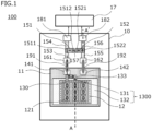
- Fig. 1 is a plan view illustrating a schematic configuration of the antenna device according to the present embodiment.
- Fig. 2 is a cross-sectional view along a line A-A' in Fig. 1 .
- a chip 11 having a quadrilateral shape on which an antenna array 12 including a plurality of antennas 121 are arranged is mounted on a substrate 10.
- Fig. 1 illustrates a configuration on a top surface of the chip 11.
- Each of the antennas 121 includes a negative differential resistance element and a resonance circuit, and transmits or receives an electromagnetic wave in a terahertz frequency band, though details of the antenna 121 will be described later.
- the antenna 121 generates an electromagnetic wave (hereinafter referred to simply as a "terahertz wave”) including a frequency band corresponding to at least a part of a frequency band (at least 30 GHz and not more than 30 THz) from a millimeter wave to the terahertz wave.
- the adjacent antennas 121 are configured to be capacitively coupled via a microstrip line (described later using Fig. 4 ).
- the chip 11 includes, in addition to the antenna array 12, a resistance element 131 and a capacitance element 132 each included in a first shunt element 1300, a pad 141 that applies a bias voltage to the chip 11, and a pad 142 that applies a ground voltage to the chip 11.
- the pads 141 and 142 are for achieving an electrical connection to a circuit outside the chip 11 and for, e.g., supplying a predetermined voltage from the outside.
- the pads 141 and 142 are made of a conductor.
- the pads are for electrical connection to the outside.
- the pads may be for a supply of a predetermined voltage from the outside and for a supply of the predetermined voltage to the outside.
- the predetermined voltage may be the ground voltage, a power source voltage, a voltage from a voltage bias circuit, or the like.
- the antenna array 12 is placed substantially at a center of the chip 11, and the capacitance element 132 is placed adjacent to the antenna array 12. Such placement of the capacitance element 132 as to surround the antenna array 12 can also enlarge an area of the capacitance element placed on the chip 11 and ensure a large capacitance.
- the capacitance element 132 is also divided to be arranged on respective sides (a right side and a left side of the chip 11 in the figure) with two facing sides of the chip 11 such that the antenna array 12 is interposed therebetween. This allows the resistance element 131, wiring, the pads, and the like to be placed in a portion (upper side of the chip 11 in the figure) where the capacitance element 132 is not placed, and can thereby reduce a chip size of the chip 11.
- one terminal of the resistance element 131 is connected to one terminal of the capacitance element 132 via each of wiring 133 and a via 134.
- the resistance element 131 and the capacitance element 132 are connected in series and, for easy placement of the connection, the resistance element 131 is preferably placed in the vicinity of the capacitance element 132. Alternatively, the resistance element 131 may also be placed on the capacitance element 132 in overlapping relation thereto.
- Another terminal of the resistance element 131 is connected to the pad 141 via a bias voltage line 130.
- the bias voltage line 130 is placed between the individual antennas 121 in the antenna array 12 to be connected commonly to the individual antennas 121 and apply the bias voltage to each of the antennas 121.
- Another terminal of the capacitance element 132 is connected to the pad 142 via wiring and a via (not shown).
- a MIM (Metal-Insulator-Metal) capacitor in which an insulating layer is interposed between metal layers can be used.
- the metal layers wiring layers in the chip 11 can be used while, as the insulating layer, an insulating layer and a dielectric layer each forming the antennas can be used.
- a grounded metal layer 124 is used, and the grounded metal layer 124 is connected to the pad 142 that applies the ground voltage.
- a metal layer 135 is formed via the insulating layer. The metal layer 135 is connected to the wiring 133 via the via 134.
- a configuration in which a capacitor is formed on a substrate other than that of the chip 11 to be bonded to the top surface or a back surface of the chip 11 is also possible, and this configuration allows a larger-capacitance capacitance element to be included.
- the resistance element 131 is connected to the pad 141 that applies the bias voltage, while the capacitance element 132 is connected to the pad 142 that applies the ground voltage.
- the number of the pads 141 for the application of the bias voltage and the number of the pads 142 that apply the ground voltage are set smaller than the number of the antennas. This allows a space of the chip 11 to be effectively used and allows a further size reduction of the chip 11. Moreover, when the number of pairs of the resistance elements 131 and the capacitance elements 132 is not more than the number of the pads 141 for the application of the bias voltage or not more than the number of the pads 142 that apply the ground voltage, it is possible to effectively use the space of the chip 11 and allow a further size reduction of the chip 11.
- the substrate 10 includes a resistance element 151 and a capacitance element 152 each included in a second shunt element 1500, a pad 161 to be connected to the pad 141 of the chip 11, and a pad 162 to be connected to the pad 142 of the chip 11.
- the pads 161 and 162 are for achieving electric connection to an external circuit outside the chip 11.
- the pads 161 and 162 are made of a conductor.
- the external circuit mentioned herein is the chip 11.
- the substrate 10 also includes a connection terminal 181 to which the bias voltage is to be supplied from the voltage bias circuit 17 and a connection terminal 182 that gives the ground voltage.
- a surface mount component SMD: Surface Mount Device
- wiring to be placed in the substrate 10 also has a resistance value, as the resistance element 151, a resistance of wiring in the substrate 10 included in a path connecting the first shunt element 1300 and the second shunt element 1500 may also be used. This can reduce the number of components used in the chip 11 and achieve a size reduction of the chip 11.
- the connection terminals 181 and 182 may also be pads herein.
- the voltage bias circuit 17 is connected from the outside of the substrate 10 via the connection terminals 181 and 182. Note that, instead of using this configuration, it may also be possible to place the voltage bias circuit 17 in the substrate 10 or in the chip 11.
- the pad 141 of the chip 11 and the pad 161 of the substrate 10 are connected with a bonding wire 191.
- the pad 142 of the chip 11 and the pad 162 of the substrate 10 are connected with a bonding wire 192.
- the pad 141 and the pad 142 are arranged appropriately on an end portion of the chip 11. Meanwhile, the pad 141 and the pad 161 are arranged appropriately to face each other with the side of the chip 11 being interposed therebetween. In addition, the pad 142 and the pad 162 are also arranged appropriately to face each other with the side of the chip 11 being interposed therebetween.
- One terminal 1512 of the resistance element 151 is connected to one terminal 1521 of the capacitance element 152 via wiring 157.
- the resistance element 151 and the capacitance element 152 are connected in series.
- the resistance element 151 and the capacitance element 152 are preferably arranged adjacent to each other. More preferably, the one terminal 1512 of the resistance element 151 is placed adjacent to the one terminal 1521 of the capacitance element 152. This can reduce a length of the wiring 157 and reduce the inductance.
- Another terminal 1511 of the resistance element 151 is connected to the pad 161 via wiring 153 and also connected to the connection terminal 181 via wiring 154.
- Another terminal 1522 of the capacitance element 152 is connected to the pad 162 via wiring 155 and also connected to the connection terminal 182 via wiring 156. It is preferable that a direction in which the terminals 1511 and 1512 of the resistance element 151 and the terminals 1521 and 1522 of the capacitance element 152 are arranged is set the same as a direction in which the pad 161 and the pad 162 are arranged. Such an arrangement can shorten the wiring to be connected and reduce the inductance.
- the resistance element 151 is connected to the connection terminal 181 to which the bias voltage is to be applied, while the capacitance element 132 is connected to the connection terminal 182 that applies the ground voltage.
- first shunt element 1300 and the second shunt element 1500 respectively include the resistance elements 131 and 151 and the capacitance elements 132 and 152.
- each of the first shunt element and the second shunt element may also be configured to include either one of the resistance element and the capacitance element.
- the shunt element includes the capacitance element, it becomes possible not only to suppress capacitive oscillation, but also reduce power consumption by using a frequency characteristic of the impedance to cut a dc current.
- Positional relationships among the components of the antenna device 100 are such that, between the antenna array 12 and the voltage bias circuit 17, the first hunt element 1300 is placed and, between the first shunt element 1300 and the voltage bias circuit 17, the second shunt element 1500 is placed.
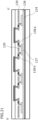
- Fig. 3 is a partial cross-sectional view of the antenna device 100 illustrating a configuration in which the pad is formed on the back surface of the chip 11 to connect the chip 11 and the substrate 10 without using bonding wires 19.
- the wiring present in the top surface of the chip 11 is connected to the pad 141 present on the back surface of the chip 11 via the through electrode 135.
- the through electrode 135 is formed by forming a through hole in the chip 11, subsequently forming an insulating film for electrical isolation on an inner wall of the through hole, and filling the through hole with copper or the like, which has a low electric resistance and can easily form an electrode by an electrolytic plating method or the like.
- the through electrode 135 is smoothed using CMP (Chemical Mechanical Polishing) processing or the like.
- CMP Chemical Mechanical Polishing
- the pad 141 on the back surface of the chip 11 and the pad 161 on the substrate 10 are arranged so as to overlap each other and connected by soldering or the like. In a case of providing the electrical connection using the through electrode 135, no bonding wire is used, and accordingly the inductance is reduced to easily suppress the parasitic oscillation in the antenna device 100.
- Figs. 4 are illustrative views illustrating the antenna array 12 in the present embodiment.
- Fig. 4A is a top view of the antenna array 12
- Fig. 4B is a cross-sectional view of the antenna array 12 along a line B-B' in Fig. 4A .
- the two antennas 121 and 122 included in the antenna array 12 are illustrated.
- each of intervals between individual antennas is set to a wavelength converted to a wavelength of an oscillating electromagnetic wave in vacuum or less, to an integral multiple of the wavelength, or more preferably to a half-wavelength or less.
- the antennas 121 and 122 are arranged such that the interval between the antennas is not more than a half-wavelength of a transmitted electromagnetic wave.
- a resonance circuit 1200 is configured to control an oscillation frequency by using a microstrip resonator including a metal layer 123 corresponding to a first conductor forming a part of each of the antennas, a dielectric layer 128, and the grounded metal layer 124 corresponding to a second conductor forming a part of each of the antennas.
- Each of the antennas 121 and 122 includes the resonance circuit 1200 and a negative differential resistance element 127.
- the bias voltage line 130 is connected via the via 135, and the bias voltage is applied to the negative differential resistance element 127.
- the negative differential resistance element 127 generates an electromagnetic wave gain for maintaining oscillation.
- the individual antennas 121 and 122 which are synchronized in the same phase to oscillate, are designed such that a frequency close to an oscillation frequency ⁇ 0 is reached. Accordingly, the individual antennas including half-wavelength resonators preferably have respective shapes similar to each other.
- the negative differential resistance elements 127 also preferably have respective shapes and characteristics equal to each other.
- a microstrip line 125 is an inter-element structure for causing individual antennas as described above to be synchronized in the same phase to oscillate.
- the microstrip line 125 which is a transmission line of a metal portion serving as an ink structure has a length from one end to another end along the microstrip line 125 which is preferably chosen to be 2 ⁇ in terms of an electric length at the oscillation frequency ⁇ 0 after the synchronization.
- the electric length of 2 ⁇ is a length corresponding to an effective oscillation wavelength ⁇ 0 converted in terms of an effective dielectric constant in a surrounding structure.
- 2 ⁇ is chosen so as to synchronize the antennas 121 and 122 in the same phase and oscillate the antennas 121 and 122. In a case of synchronizing the antennas 121 and 122 in opposite phases, the electric length may also be ⁇ or 3 ⁇ .
- the length of the microstrip line 125 is not precisely 2 ⁇ , the synchronization of the antennas 121 and 122 is possible.
- an electric length of about 2 ⁇ 10% is typically in an allowable range. Note that the allowable range is wider than when coupling is provided without using the microstrip line 125. Note that the electric length of the microstrip line can easily be checked with an electromagnetic field simulator or the like.
- a part of an oscillation output of the antenna 121 is input in substantially the same phase to the adjacent antenna 122 via the microstrip line 125. Meanwhile, a part of an oscillation output of the antenna 122 is input in substantially the same phase to the adjacent antenna 121 via the microstrip line 125.
- the microstrip line 125 has been introduced.
- the microstrip line 125 in the present embodiment is characterized by capacitive coupling with the metal layer 123 of a resonance structure.
- the microstrip line 125 and the metal layer 123 only form a capacitor via the insulating layer 129 in a metal-insulator-metal (MIM) region 126, and are DC-open. Accordingly, in a band of the oscillation frequency ⁇ 0 , antenna-to-antenna coupling of a magnitude as large as that of direct coupling can be ensured. In addition, in a low frequency region lower than ⁇ 0 , the magnitude of the coupling decreases, and therefore it is possible to ensure isolation between the antennas.
- the microstrip line 125 in the present embodiment having such a property is preferable.
- the microstrip line 125 having open end portions serves as a capacitive element.
- the microstrip line 125 is the capacitive element, and the metal layer 123 of the resonance structure on an antenna 122 side is also a capacitor.
- the plurality of metal layers 123 corresponding to the number of the arrays are placed via the dielectric layer 128, and the negative differential resistance elements 127 corresponding to the metal layers 123 are placed.
- the adjacent antennas are capacitively coupled via the microstrip lines 125.
- Each of the microstrip lines 125 has an electric length of about 2 ⁇ . Accordingly, it becomes possible to synchronize all the negative differential resistance elements 127 in the same phase. As a result of thus arraying the antennas, not only synthesized electric power is increased, but also a sharp directionality is favorably obtained.
- the plurality of metal layers 123 are connected commonly via a strip conductor (not shown) to be connected to the pad 141 to which the bias voltage is to be applied, while the grounded metal layer 124 is connected to the pad 142 inside the chip 11.
- the bias voltage is applied to the negative differential resistance elements 127.
- each of the negative differential resistance elements 127 a resonant tunneling diode that is lattice-matched to an InP substrate can be used.
- the negative differential resistance element 127 is not limited to the resonant tunneling diode, and an Esaki diode or a Gunn diode may also be used.
- the resonance tunnelling diode is configured to include, e.g., a multiple quantum well structure including InGaAs/InAlAs and InGaAs/AlAs on the InP substrate and an electric contact layer including n-InGaAs.
- the multiple quantum well structure e.g., a triple-barrier structure is used.
- the multiple quantum well structure is formed of a semiconductor multilayer film structure including AlAs (1.3 nm)/InGaAs (7.6 nm)/InAlAs (2.6 nm)/InGaAs (5.6 nm)/AlAs (1.3 nm).
- InGaAs is a well layer
- lattice-matched InAlAs and non-matched AlAs are barrier layers. These layers are intentionally left undoped by not performing carrier doping.
- Such a multiple quantum well structure is interposed between the electric contact layers including n-InGaAs at an electron density of 2 ⁇ 10 18 cm -3 .
- a current-voltage (I/V) characteristic of such a structure between the electric contact layers has a peak current density of 280 kA/cm 2 , and a negative resistance region ranges from about 0.7 V to about 0.9 V.
- a peak current value of 10 mA and a negative resistance value of -20 S2 are obtained.
- an oscillation frequency is about 0.55 THz.
- Fig. 5 illustrates an equivalent circuit diagram of the antenna device according to the present embodiment.
- An equivalent circuit of the chip 11 has a resistance r of each of the negative differential resistance elements included in the antenna array 12 (r represents an absolute value of a resistance of the negative differential resistance element).
- the equivalent circuit of the chip 11 also has an impedance Z of the resonance circuit 1200 included in the antenna array 12 and a resistance Rc of the resistance element 131 included in the first shunt element 1300.
- the equivalent circuit of the chip 11 further has a capacitance Cc of the capacitance element 132 included in the first shunt element 1300.
- the first shunt element 1300 is configured to include the resistance Rc and the capacitance Cc which are connected in series.
- the resistance r, the impedance Z of the resonance circuit 1200, and the first shunt element 1300 are connected in parallel to each other. More specifically, one terminal of the resistance r, one terminal of the impedance Z of the resonance circuit 1200, and one terminal of the resistance Rc are each connected to a first node n1. Meanwhile, another terminal of the resistance Rc is connected to one terminal of the capacitance Cc. In addition, another terminal of the resistance r, another terminal of the impedance Z of the resonance circuit 1200, and another terminal of the capacitance Cc are connected to the ground voltage.
- the first node n1 is connected to the pad 141 of the chip 11, and the ground voltage is applied via the pad 142 of the chip 11.
- An equivalent circuit of the substrate 10 is configured to include a resistance Rp of the resistance element 151 included in the second shunt element 1500, a capacitance Cp of the capacitance element 152 included therein, and an inductance L of the path connecting the first shunt element 1300 and the second shunt element 1500.
- the inductance L includes respective parasitic inductances of the wiring connecting the first shunt element 1300 and the pad 141, the bonding wires connecting the chip and the substrate, and the wiring, the pads, and the like connecting the bonding wires and the second shunt element 1500.
- the second shunt element 1500 is configured to include the resistance Rp and the capacitance Cp which are connected in series.
- the chip 11 and the second shunt element 1500 are connected via the inductance L. More specifically, one terminal of the inductance L is connected to the first node n1 in the equivalent circuit of the chip 11, and another terminal of the inductance L and one terminal of the resistance Rp are connected to a second node n2. Meanwhile, another terminal of the resistance Rp is connected to one terminal of the capacitance Cp. To another terminal of the capacitance Cp, the ground voltage is applied.
- the second node n2 is further connected to the terminal 181, and a voltage bias circuit V is connected thereto. Consequently, to the second node n2, the bias voltage is applied and, to the resistance r, the bias voltage is applied via the inductance L.
- the first shunt element 1300 (the resistance Rc and the capacitance Cc) is connected in parallel to the negative differential resistance element (the resistance r), and is also connected in parallel to the second shunt element 1500 (the resistance Rp and the capacitance Cp) via the inductance L. Furthermore, the first shunt element 1300 is also connected in parallel to the voltage bias circuit V.
- each of the first shunt element 1300 and the second shunt element 1500 has a low impedance with respect to the resistance r of the negative differential resistance element 127 used as a reference.
- each of the first shunt element 1300 and the second shunt element 1500 is preferably set to have a low impedance when viewed from the negative differential resistance element 127.
- Rp is a resistance value of the resistance Rp corresponding to a second resistor
- Cp is a capacitance value of the capacitance Cp corresponding to a second capacitor
- L is the inductance of the path connecting the first shunt element 1300 and the second shunt element 1500.
- f represents a frequency of the targeted parasitic oscillation, which is a frequency less than a resonance frequency of each of the resonance circuits included in the antenna array 12.
- the frequency f is specifically less than 30 GHz, and is particularly a frequency in a range of 10 MHz to 10 GHz in a case where the chip 11 is mounted on the substrate 10 used in the present embodiment.
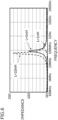
- Fig. 6 is a graph representing a frequency characteristic of the impedance when viewed from the negative differential resistance element 127 when a value of the inductance L is varied on the basis of the equivalent circuit in Fig. 5 .
- a solid line represents a characteristic with respect to 5 nH
- a dash-dot line represents a characteristic with respect to 10 nH
- the impedance has a peak value at a specified frequency.
- a peak value is 1.8 S2 at 160 MHz
- a peak value is 16.8 S2 at 50 MHz
- a peck value is 8.5 S2 at 71 MHz.
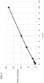
- Fig. 7 is a graph representing a relationship between the inductance L and the peak value of the inductance when viewed from the negative differential resistance element 127 on the basis of the frequency characteristic in Fig. 6 . According to Fig. 7 , as the inductance L increases, the peak value of the impedance increases.
- the inductance L includes the respective parasitic inductances of the wiring connecting the first shunt element 1300 and the pad 141, the bonding wires connecting the chip and the substrate, and the wiring, the pads, and the like connecting the bonding wires and the second shunt element 1500.
- Each of these inductances of the path connecting the first shunt element 1300 and the second shunt element 1500 can be calculated using Expressions (4) and (5) below.
- Expression (4) a portion having a cross section that can be approximated to a substantially circular shape is calculated using Expression (4), while a portion thereof having a cross section that can be approximated to a quadrilateral shape is calculated using Expression (5).
- L 1 0.2 ⁇ l 1 ⁇ ln 4 ⁇ l 1 / d ⁇ 0.75 nH
- L 2 0.2 ⁇ l 2 ⁇ ln 2 ⁇ l 2 / w + h + 0.2235 ⁇ w + h / l 2 + 0.5 nH
- 11 is a length (mm) of the portion of the path having the cross section that can be approximated to the substantially circular shape
- d is a diameter (mm) of a cross section thereof.
- l2 is a length (mm) of the portion of the path having the cross section that can be approximated to the quadrilateral shape
- w is a width (mm) thereof
- h is a thickness (mm) thereof.
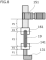
- Fig. 8 is a diagram illustrating the inductance of the path connecting the first shunt element 1300 and the second shunt element 1500 in the present embodiment.
- the path connecting the first shunt element 1300 and the second shunt element 1500 has wiring (first portion P1) connecting the resistance element 131 included in the first shunt element 1300 and the pad 141 as well as the pad 141 (second portion P2).
- the path further has the bonding wire 19 (third portion P3), the pad 161 (fourth portion P4), and wiring (fifth portion P5) connecting the pad 161 and the resistance element 151 included in the second shunt element 1500.
- a length of the path connecting the first shunt element 1300 and the second shunt element 1500 is preferably not more than 4 mm, which is appropriate to reduce the parasitic inductance and suppress the parasitic oscillation. More preferably, the length of the path is not more than 2 mm.
- the first portion P1 has a length of 0.3 mm, a width of 0.2 mm, and a thickness of 0.5 ⁇ m, and an inductance L1 of this region is calculated using Expression (5) to be 0.1 nH.
- An inductance L2 of the second portion P2 is calculated on the assumption that the second portion P2 is a region from an end portion of the pad 141 to substantially a center portion of the pad 141 to which the bonding wire 19 is connected.
- This region has a length of 0.1 mm, a width of 0.2 mm, and a thickness of 0.5 ⁇ m, and the inductance L2 of this region is calculated using Expression (5) to be 0.02 nH.
- the third portion P3 is the bonding wire having a length of 1.0 mm and a cross section diameter of 20 ⁇ m, and an inductance L3 of this region is calculated using Expression (4) to be 0.91 nH.
- An inductance L4 of the fourth portion P4 is calculated on the assumption that the fourth portion P4 is a region from an end portion of the pad 161 to substantially a center portion of the pad 161 to which the bonding wire 19 is connected. This region has a length of 0.6 mm, a width of 1.2 mm, and a thickness of 35 ⁇ m, and the inductance L4 is calculated using Expression (5) to be 0.11 nH.
- the fifth portion P5 has a length of 0.8 mm, a width of 0.6 mm, and a thickness of 35 ⁇ m, and an inductance L5 of this region is calculated using Expression (5) to be 0.26 nH.
- the inductance of the path connecting the first shunt element 1300 and the second shunt element 1500 can be calculated as a total of the inductances L1, L2, L3, L4, and L5 to be 1.4 nH.
- the inductance is calculated using Expression (4) on the assumption that the bonding wire 19 has a circular cross section, but it may also be possible to use a ribbon-shaped bonding wire having a quadrilateral cross section.
- the inductance can be calculated using Expression (5).
- the ribbon-shaped bonding wire can have a large cross-sectional area, and the inductance can be reduced.
- Figs. 9A and 9B are diagrams illustrating the calculation of the inductance of the wiring. A description will be given herein by using the wiring 153 connecting the pad 161 and the resistance element 151 included in the second shunt element 1500. The wiring connecting the resistance element 131 included in the first shunt element 1300 and the pad 141 can also be considered in the same manner.
- Fig. 9A is a diagram illustrating an example of a configuration in which the wiring 153 has bent portions.
- the wiring 153 is configured to include the bent portions having two 90-degree bent portions.
- the inductance of the wiring 153 in the example illustrated in Fig. 9A can be calculated by dividing the wiring 153 into three rectangular portions.
- the three rectangular portions are a first rectangular portion RS1 connected to the pad 161, a second rectangular portion RS2 connected to the first rectangular portion, and a third rectangular portion RS3 connected to the second rectangular portion.
- the third rectangular portion RS3 is connected to the resistance element 151.
- the first rectangular portion RS1 has a length l21, a width w1, and a thickness h1
- the second rectangular portion RS2 has a length l22, a width w2, and a thickness h2
- the third rectangular portion RS3 has a length l23, a width w3, and a thickness h3.
- a distance between the end portion of the pad 161 and the point A is the length l21 of the first rectangular portion
- a distance between the point A and the point B is the length l22 of the second rectangular portion RS2
- a distance between the point B and an end portion of the resistance element 151 is the length l23 of the third rectangular portion RS3.
- a determination method other than that described above may also be adopted as long as the wiring 153 is divided, and the rectangular portions can be specified.
- Fig. 9B is a diagram illustrating an example in which the wiring 153 is configured to linearly extend, while a width thereof gradually increases from the resistance element 151 toward the pad 161. Even with the wiring 153 thus configured, by replacing the wiring 153 with a rectangular portion RS4 as illustrated in the figure, it is possible to calculate the inductance of the wiring 153 by using Expression (5).
- the rectangular portion RS4 has a length l24, a width w4, and a thickness h4.
- a center point C of a portion V-V' along which the wiring 153 and the pad 161 are in contact is defined, and a point D which allows contact with the resistance element 151, while having a shortest distance to the point C, is defined. It is assumed that the distance between the point C and the point D is the length l24. It is also assumed that a distance between end portions of the wiring in a direction perpendicular to a line segment CD via a middle E between the point C and the point D is the width w4.
- the inductance of the wiring can be calculated.
- the parasitic oscillation can be suppressed.
- the inductance L of the path connecting the first shunt element 1300 and the second shunt element 1500, which is used in Expression (3) is determined, it is possible to apply the calculation methods described using Expression (4), Expression (5), Fig. 8 , and Fig. 9 .
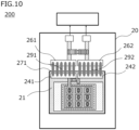
- a pad and a pad are connected with a plurality of bonding wires. Note that, in the present embodiment, a description of the same components as those in the first embodiment is omitted.
- a chip 21 includes a pad 241 for applying a bias voltage and a pad 242 that applies a ground voltage.
- a substrate 20 includes a pad 261 for connection to the pad 241 of the chip 21 and a pad 262 for connection to the pad 242 of the chip 21.
- the substrate 20 also has a plurality of bonding wires 291 for connecting the pad 241 and the pad 261 and a plurality of bonding wires 292 for connecting the pad 242 and the pad 262.
- an antenna array, a first shunt element, a second shunt element, and the like in the antenna device 200 are the same as those in the antenna device 100 in the first embodiment.
- the pad 241 and the pad 261 are arranged as well as the pad 242 and the pad 262 adjacent to each other and thereby shorten the bonding wires 291 and 292.
- the pad 241 and the pad 242 are preferably placed on end portions of the chip 21.
- a side of the chip 21 traversed by the plurality of bonding wires 291 and 292 is a first side 271
- the pad 241 and the pad 261 are arranged so as to face each other with the first side 271 being interposed therebetween.
- the pad 242 and the pad 262 are also arranged so as to face each other with the first side 271 being interposed therebetween.
- the plurality of bonding wires 291 and 292 are arranged side by side to be spaced apart from each other in a direction parallel to the first side 271.
- the plurality of bonding wires 291 and 292 are electrically connected in parallel.
- a combined inductance Lm of M bonding wires connected in parallel can be calculating using Expression (6) below.
- Li is an inductance of the i-th bonding wire among the M bonding wires and, when the bonding wires have circular cross sections, the calculation is performed using Expression (4) while, when the bonding wires have quadrilateral cross sections, the calculation is performed using Expression (5). Note that whether the bonding wires have the circular cross sections or the quadrilateral cross sections may be determined as appropriate, and the combined inductance Lm of the bonding wires may appropriately be calculated using Expressions (4) and (5).
- areas of the pads 241 and 242 are set larger than those of the pads 141 and 142 in the first embodiment, and areas of the pads 261 and 262 are set larger than those of the pads 161 and 162 in the first embodiment.
- the pads 241, 242, 261, and 262 are configured such that dimensions thereof in directions parallel to the first side 271 of the chip 21 are larger than dimensions thereof in directions perpendicular to the first side 271. This can increase the number of the bonding wires that can be placed and reduce the combined inductance of the bonding wires.
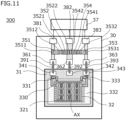
- FIG. 11 a description will be given of an antenna device according to the third embodiment of the present disclosure.
- the third embodiment is different from the first embodiment in that additional resistance elements and capacitance elements are included in a first shunt element and a second shunt element to be connected in parallel.
- a description of the same components as those in the first and second embodiments is omitted.
- a chip 31 includes a first shunt element including a resistance element 331 and a capacitance element 332 and another first shunt element including a resistance element 333 and the capacitance element 332.
- the chip 31 includes pads 341 and 343 for applying a bias voltage and a pad 342 that applies a ground voltage.
- a substrate 30 includes a second shunt element including a resistance element 351 and a capacitance element 352 and another second shunt element including a resistance element 353 and a capacitance element 354.
- the substrate 30 also includes a pad 361 for connection to the pad 341 of the chip 31, a pad 362 for connection to the pad 342 of the chip 31, and a pad 363 for connection to the pad 343 of the chip 31.
- the pad 341 and the pad 361 are connected with a bonding wire 391, the pad 342 and the pad 362 are connected with a bonding wire 392, and the pad 343 and the pad 363 are connected with a bonding wire 393.
- the substrate 30 further includes connection terminals 381 and 383 to which the bias voltage is applied from a voltage bias circuit 37 and the connection terminal 182 that gives the ground voltage.
- the pads 341, 342, and 343 of the chip 31 and the pads 361, 362, and 363 of the substrate 30 are connected, on a one-to-one basis, with the respective bonding wires 391, 392, and 393.
- the two pads may also be connected with a plurality of bonding wires.
- the two pads may also be connected with through electrodes instead of using the bonding wires 391, 392, and 393.
- An antenna array 32 is placed at substantially a center of the chip 31 in the same manner as in the first embodiment, and the capacitance element 332 is placed adjacent to the antenna array 32.
- One terminal of the resistance element 331 is connected to one terminal of the capacitance element 332 via wiring and a via (not shown).
- One terminal of the resistance element 333 is connected to one terminal of the capacitance element 332 via wiring and a via (not shown).
- the resistance elements 331 and 333 are preferably placed in the vicinity of the capacitance element 332. Alternatively, the resistance elements 331 and 333 may also be placed on the capacitance element 332 in overlapping relation thereto.
- Another terminal of the resistance element 331 is connected to the pad 341 via a bias voltage line 330.
- the bias voltage line 330 is placed also between individual antennas 321 of the antenna array 32 to be connected to each of the antennas 321. Thus, the bias voltage is applied to each of the antennas 321.
- Another terminal of the capacitance element 332 is connected to the pad 342 via wiring and a via (not shown).
- Another terminal of the resistance element 333 is connected to the pad 343 via the bias voltage line 330.
- One terminal 3512 of the resistance element 351 is connected to the one terminal 3521 of the capacitance element 352 via wiring.
- the resistance element 351 and the capacitance element 352 are connected in series. Accordingly, the resistance element 351 and the capacitance element 352 are preferably arranged adjacent to each other. More preferably, the one terminal 3512 of the resistance element 351 is placed adjacent to the one terminal 3521 of the capacitance element 352 to be able to shorten the wiring and reduce the inductance.
- Another terminal 3511 of the resistance element 351 is connected to the pad 361 via wiring and also connected to the connection terminal 381 via the wiring.
- another terminal 3522 of the capacitance element 352 is connected to the pad 362 via wiring, and is also connected to a connection terminal 382 via wiring.
- One terminal 3532 of the resistance element 353 is connected to one terminal 3541 of the capacitance element 354 via wiring.
- the resistance element 353 and the capacitance element 354 are connected in series. Accordingly, the resistance element 353 and the capacitance element 354 are preferably arranged adjacent to each other. More preferably, the one terminal 3532 of the resistance element 353 and the one terminal 3541 of the capacitance element 354 are arranged adjacent to each other to be able to shorten the wiring and reduce the inductance.
- Another terminal 3531 of the resistance element 353 is connected to the pad 363 via wiring, and is also connected to the connection terminal 383 via wiring.
- another terminal 3542 of the capacitance element 354 is connected to the pad 362 via wiring, and is also connected to the connection terminal 382 via wiring.
- the terminals 3511 and 3512 of the resistance element 351, the terminals 3521 and 3522 of the capacitance element 352, the terminals 3531 and 3532 of the resistance element 353, and the terminals 3541 and 3542 of the capacitance element 354 are arranged side by side in one direction (left-right direction in the figure) over the substrate 30.
- the pads 361, 362, and 363 are also arranged side by side in the same direction as the direction in which the terminals 3511, 3512, 3521, 3522, 3531, 3532, 3541, and 3542 are arranged.
- the other terminal 3511 of the resistance element 351 and the other terminal 3531 of the resistance element 353 are electrically connected.
- the other terminal 3522 of the capacitance element 352 and the other terminal 3542 of the capacitance element 354 are commonly connected via the wiring.
- the resistance element 351 and the capacitance element 352 each included in the second shunt element and the resistance element 353 and the capacitance element 354 each included in the other second shunt element are electrically connected in parallel.
- each of the resistance elements 351 and 353 and the capacitance elements 352 and 354 e.g., a SMD (Surface Mount Device) is adopted, and such a component has not only a resistive component and a capacitive component, but also a parasitic inductance. Accordingly, in two pairs of the first shunt elements and the second shunt elements, the second shunt elements in the respective pairs (the resistance element 351, the capacitance element 352, the resistance element 353, and the capacitance element 354) are connected in parallel. Thus, it is possible to reduce the parasitic inductance and suppress the parasitic oscillation.
- a SMD Surface Mount Device
- bonding wire 391 and the bonding wire 393 each serving as a path that supplies the bias voltage are connected in parallel, a combined inductance of the bonding wires is also reduced.
- the wiring placed in the substrate 30 also has a resistance value, as each of the resistance elements 351 and 353, a resistance of the wiring in the substrate 30 connecting the first shunt elements and the second shunt elements may also be used. This can reduce the number of components to be placed over the substrate 30, which is advantageous for a size reduction.
- the elements and pads that are arranged over the chip 31 and the elements, pads, wiring, and the like arranged over the substrate 30 are arranged symmetrically with respect to an axis passing through a center of the antenna array 32.
- the axis passing through the center of the antenna array 32 include an axis AX extending in a direction perpendicular to the top surface of the substrate 30 and an axis extending in a direction parallel to the top surface of the substrate 30. Symmetricity is determined herein on the basis of the axis extending in the direction parallel to the top surface of the substrate.
- the center of the antenna array 32 can be determined on the basis of a planar shape of the conductor of the antenna array 32.
- the center of the antenna array 32 may also be a gravity center of the conductor of the antenna array 32.
- the gravity center can be determined on the basis of a cross-sectional shape and a planar shape. Therefore, in the substrate 30, the plurality of pairs of the first shunts and the second shunt elements which are connected to each other are arranged, and at least two of the pairs of the first shunt elements and the second shunt elements are placed at positions symmetrical to each other with respect to the axis passing through the center of the antenna array. This improves a directionality of a terahertz wave generated from the antenna array 32 and enhances a frontal intensity of the terahertz wave.
- a configuration is adopted in which the bias voltage is supplied from two paths using the connection terminals 381 and 383, and the ground voltage is given from one path using the connection terminal 182.
- the ground voltage is given from the two paths using the connection terminals 381 and 383, and the bias voltage is supplied from the one path using the connection terminal 182.
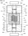
- the antenna device according to the fourth embodiment is different from the antenna device according to the first embodiment in that pads are arranged on both sides on which two facing sides of a chip are present, i.e., the pads and the chip are arranged such that the chip is interposed between the pads.
- the pads and the chip are arranged such that the chip is interposed between the pads.
- a chip 41 includes, in the same manner as in the first embodiment, a pad 441 for applying a bias voltage and a pad 442 that applies a ground voltage.
- the antenna device 400 includes a pad 443 for applying the bias voltage and a pad 444 for applying the ground voltage.
- the pads 441 and 442 are arranged on a side on which a first side 411 of the chip 41 is present when viewed from an antenna array 42.
- the pad 443 and the pad 444 are arranged on a side on which a second side 412 of the chip 41 facing the first side 411 is present when viewed from the antenna array 42.
- a resistance element 431, a capacitance element 432, and a resistance element 433 which are included in the first shunt element are arranged.
- One terminal of the resistance element 431 is connected to one terminal of the capacitance element 432 via wiring and a via (not shown).
- the resistance element 431 is placed in the vicinity of the capacitance element 432.
- the resistance element 431 may also be placed on the capacitance element 432 in overlapping relation thereto.
- another terminal of the resistance element 431 is connected to the pad 441 via a bias voltage line 430.
- the bias voltage line 430 is placed also between the individual antennas 421 of the antenna array 42 to be connected commonly to the individual antennas 421, and the bias voltage is applied to each of the antennas 421.
- One terminal of the resistance element 433 is connected to one terminal of the capacitance element 432 via wiring and a via (not shown).
- the resistance element 433 is placed in the vicinity of the capacitance element 432.
- the resistance element 433 may also be placed on the capacitance element 432 in overlapping relation thereto.
- another terminal of the resistance element 433 is connected to the pad 443 via the bias voltage line 430.
- Another terminal of the capacitance element 432 is connected to the pads 442 and 444 via wiring a vias (not shown).
- the resistance element 431 and the resistance element 433 are arranged. Meanwhile, between the resistance element 431 and the resistance element 433, the antenna array 42 around which the capacitance element 432 is placed is placed.
- the pads and the first shunt element are arranged symmetrically with respect to an axis passing through a center of the antenna array 42 (an axis BX that is c on a top surface of the substrate 40).
- the plurality of pairs of the first shunts and the second shunt elements which are connected to each other are arranged, and at least two of the pairs of the first shunt elements and the second shunt elements are arranged at positions symmetrical to each other with respect to the axis passing through the center of the antenna array. This improves a directionality of a terahertz wave generated from the antenna array 42 and enhances a frontal intensity of the terahertz wave.
- a resistance element 451 and a capacitance element 452 each included in the second shunt element are arranged in the first region 413.
- a pad 461 to be connected to the pad 441 of the chip 41 with a bonding wire 491 and a pad 462 to be connected to the pad 442 of the chip 41 with a bonding wire 492 are arranged in the first region 413.
- a connection terminal 481 to which the bias voltage is to be supplied from a voltage bias circuit 471 and a connection terminal 482 that gives the ground voltage are arranged.
- a resistance element 453 and a capacitance element 454 each included in the second shunt element are arranged in a second region 414 (region surrounded by a dotted line in the figure) present on the side of the chip 41 with the second side 412.
- a pad 463 to be connected to the pad 443 of the chip 41 with a bonding wire 493 and a pad 464 to be connected to the pad 444 of the chip 41 with a bonding wire 494 are arranged.
- a connection terminal 483 to which the bias voltage is to be supplied from a voltage bias circuit 472 and a connection terminal 484 that gives the ground voltage are arranged in the second region 414.
- the voltage bias circuits 471 and 472 are provided as separate circuits, but the substrate 40 may also be configured such that one voltage bias circuit supplies the bias voltage and the ground voltage.
- the substrate 40 has a configuration in which the chip 41 is placed between the first region 413 and the second region 414.
- the antenna array 42 is placed between the pads 441 and 442 and the pads 443 and 443, the antenna array 42 is placed.
- the first region 413, the chip 41, and the second region 414 are arranged in this order.
- Such a configuration can reduce the impedance of the wiring that supplies the bias voltage.
- the resistance element 451 or the capacitance element 452 and the resistance element 453 or the capacitance element 454 the chip 41 is placed.
- the pads and the second shunt elements are arranged symmetrically with respect to the axis passing through the center of the antenna array 42.
- the axis passing through the center of the antenna array 42 include the axis BX extending in the direction perpendicular to the top surface of the substrate 40 and an axis extending in a direction parallel to the top surface of the substrate 40. Symmetricity is determined herein on the basis of the axis extending in the direction parallel to the top surface of the substrate.
- the plurality of pairs of the first shunts and the second shunt elements which are connected to each other are arranged, and at least two of the pairs of the first shunt elements and the second shunt elements are arranged at positions symmetrical to each other with respect to the axis passing through the center of the antenna array. This improves the directionality of the terahertz wave generated from the antenna array 42 and enhances the frontal intensity of the terahertz wave.
- the bias voltage to be applied to the antenna array 42 is supplied from the side of the chip 41 with the two facing sides 411 and 412.
- the impedance of the wiring that supplies the bias voltage is smaller than in a case where the bias voltage is supplied from a side of the chip 41 with any one of the sides, and accordingly a voltage drop is reduced. Consequently, antenna-to-antenna variation in the bias voltage to be applied to the negative differential resistance element of each of the antennas decreases to improve uniformities of antenna outputs.
- the resistance element 451 and the capacitance element 452 and the resistance element 453 and the capacitance element 454, which are included in the second shunt elements, are connected in parallel.
- the resistance elements 451 and 453 and the capacitance elements 452 and 454, e.g., the SMD is adopted, and such a component has not only a resistive component and a capacitive component, but also a parasitic inductance. Accordingly, by connecting the resistance element 451 and the capacitance element 452 and the resistance element 453 and the capacitance element 454 in parallel, it is possible to reduce the parasitic inductance and suppress the parasitic oscillation.
- the wiring placed in the substrate 40 also has a resistance value, as each of the resistance elements 451 and 453, a resistance of the wiring may also be used, and the number of components to be placed over the substrate 40 can thus be reduced, which is advantageous for a size reduction.
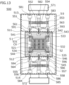
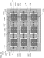
- Fig. 13 is a diagram illustrating an antenna device according to a modification of the present embodiment. Note that, in the present modification, a description of the same components as those in the embodiments described above is omitted.
- a configuration of an antenna device 500 illustrated in Fig. 13 corresponds to a configuration obtained by further applying characteristic features of the present embodiment to the configuration illustrated in the third embodiment.
- the same components as those in the third embodiment are denoted by the same reference signs, and a description thereof is omitted.
- resistance elements 531 and 533 and pads 541, 542, and 543 are arranged in the same manner as in the third embodiment. Meanwhile, on a side of the chip 51 on which a second side 512 thereof facing the first side 511 is present, resistance elements 534 and 535 and pads 544, 545, and 546 are arranged.
- an antenna array 52 in which a plurality of antennas 521 are arranged is placed.
- the capacitance element 532 is placed.
- the capacitance element 532 is connected to each of the resistance elements 531, 533, 534, and 535 to be included in a first shunt element.
- Respective one terminals of the resistance elements 531, 533, 534, and 535 are connected to one terminal of the capacitance element 532 via wiring and vias (not shown).
- the resistance elements 531, 533, 534, and 535 are preferably arranged in the vicinity of the capacitance element 532.
- the resistance elements 531, 533, 534, and 535 may also be placed on the capacitance element 532 in overlapping relation thereto.
- Respective other terminals of the resistance elements 531, 533, 534, and 535 are connected to the pad 541 via a bias voltage line 530.
- the bias voltage line 530 is placed also between the individual antennas 521 in the antenna array 52 to be connected commonly to the individual antennas 521, and a bias voltage is applied to each of the antennas 521.
- Another terminal of the capacitance element 532 is connected to the pads 542 and 545 via wiring and vias (not shown).
- the resistance elements 531 and 533 and the resistance elements 534 and 535 are arranged.
- the antenna array 52 around which the capacitance element 532 is placed is placed.
- the pads and the first shunt elements are arranged symmetrically with respect to an axis passing through a center of the antenna array 52.
- the axis passing through the center of the antenna array 52 include an axis CX extending in a direction perpendicular to a top surface of a substrate 50 and an axis extending in a direction parallel to the top surface of the substrate 50.
- Symmetricity is determined herein on the basis of the axis extending in the direction parallel to the top surface of the substrate. Therefore, in the substrate 50, the plurality of pairs of the first shunts and second shunt elements which are connected to each other are arranged, and at least two of the pairs of the first shunt elements and the second shunt elements are arranged at positions symmetrical to each other with respect to the axis passing through the center of the antenna array. This improves a directionality of a terahertz wave generated from the antenna array 52 and enhances a frontal intensity of the terahertz wave.
- a pad 561 to be connected to the pad 541 of the chip 51 with a bonding wire 591 is placed in a first region 513 (region surrounded by a dotted line in the figure) present on the side of the chip 51 with the first side 511.
- a pad 562 to be connected to the pad 542 with a bonding wire 592 and a pad 563 to be connected to the pad 543 with a bonding wire 593 are arranged in the first region 513.
- resistance elements 551 and 553 and capacitance elements 552 and 554 which are included in the second shunt elements are arranged in the first region 513.
- connection terminal 581 and 583 to which the bias voltage is to be supplied from a voltage bias circuit 571 as well as a connection terminal 582 that gives the ground voltage are arranged. Note that mutual connection relationships between the individual pads, the second shunt elements, and the connection terminals are the same as the connection relationships described in the third embodiment.
- the voltage bias circuits 571 and 572 are provided as separate circuits, but the substrate 50 may also be configured such that one voltage bias circuit supplies the bias voltage and the ground voltage.
- a pad 564 to be connected to the pad 544 of the chip 51 with a bonding wire 594 is placed in a second region 514 (region surrounded by a dotted line in the figure) present on the side of the chip 51 with the second side 512.
- a pad 565 to be connected to the pad 545 with a bonding wire 595 and a pad 566 to be connected to the pad 546 with a bonding wire 596 are arranged in the second region 514.
- resistance elements 555 and 557 and capacitance elements 556 and 558 which are included in the second shunt elements are arranged in the second region 514.
- connection terminal 584 and 586 to which the bias voltage is to be supplied from the voltage bias circuit 572 as well as a connection terminal 585 that gives the ground voltage are arranged. Note that connection relationships among the individual pads, the second shunt elements, and the connection terminals in the second region 514 are also the same as the connection relationships described in the third embodiment.
- the substrate 50 has a configuration in which the chip 51 is placed between the first region 513 and the second region 514.
- the antenna array 52 is placed between the pad 541 and the pad 544, between the pad 542 and the pad 545, or between the pad 543 and the pad 546.
- the chip 51 is placed between the resistance elements 551 and 553 and the capacitance elements 552 and 554 and between the resistance elements 555 and 557 and the capacitance elements 556 and 558.
- the pads and the second shunt elements are arranged symmetrically with respect to the axis passing through the center of the antenna array 52.
- Examples of the axis passing through the center of the antenna array 52 include the axis CX extending in the direction perpendicular to the top surface of the substrate 50 and an axis extending in a direction parallel to the top surface of the substrate 50. Symmetricity is determined herein on the basis of the axis extending in the direction parallel to the top surface of the substrate. Therefore, in the substrate 50, the plurality of pairs of the first shunts and the second shunt elements which are connected to each other are arranged, and at least two of the pairs of the first shunt elements and the second shunt elements are arranged at positions symmetrical to each other with respect to the axis passing through the center of the antenna array. This improves a directionality of a terahertz wave generated from the antenna array 52 and enhances a frontal intensity of the terahertz wave.
- the impedance of the wiring that supplies the bias voltage decreases, and accordingly a voltage drop is reduced. Consequently, antenna-to-antenna variation in the bias voltage to be applied to the negative differential resistance element of each of the antennas decreases to improve uniformities of antenna outputs.
- the resistance element 551 and the capacitance element 552 and the resistance element 553 and the capacitance element 554, which are included in the second shunt element, are connected in parallel.
- the resistance element 555 and the capacitance element 556 and the resistance element 557 and the capacitance element 558, which are included in the second shunt element are connected in parallel. Accordingly, in the antenna device 500, the number of the resistance elements and the capacitance elements which are connected in parallel is larger than that in the antenna device 400. Therefore, it is possible to further reduce the parasitic inductance included in the resistance elements and the capacitance elements and suppress the parasitic oscillation.
- the wiring placed in the substrate 50 also has a resistance value, as each of the resistance elements 551, 553, 555, and 557, a resistance of the wiring may also be used, and the number of components to be placed over the substrate 50 can thus be reduced, which is advantageous for a size reduction.
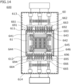
- Fig. 14 is a diagram illustrating an antenna device according to a modification of the present embodiment.
- a configuration of an antenna device 600 illustrated in Fig. 14 corresponds to a configuration obtained by further applying characteristic features of the second embodiment to the configuration of the antenna device 500 illustrated in Fig. 13 .
- the antenna device according to the present modification is characterized in that the number of the bonding wires providing connection between the pads in the antenna device described above is different.
- a description of the same components as those of the antenna device 500 illustrated in Fig. 13 is omitted.
- pads 641, 642, and 643 are arranged on a side of the chip 61 on which a first side 611 of the chip 61 is present.
- pads 644, 645, and 646 are arranged on a side of the chip 61 on which a second side 612 thereof facing the first side 611 is present.
- pads 661, 662, and 663 are arranged, in the same manner as in the configuration illustrated in Fig. 13 .
- pads 664, 665, and 666 are arranged in a substrate 60.
- the pad 641 and the pad 661 are connected with a plurality of bonding wires 691
- the pad 642 and the pad 662 are connected with a plurality of bonding wires 692
- the pad 643 and the pad 663 are connected with a plurality of bonding wires 693.
- the pad 644 and the pad 664 are connected with a plurality of bonding wires 694
- the pad 645 and the pad 665 are connected with a plurality of bonding wires 695
- the pad 646 and the pad 666 are connected with a plurality of bonding wires 696.
- the antenna device according to the fifth embodiment is characterized in that pads are arranged in the vicinity of individual sides of a chip.
- a description of the same components as those in the other embodiments is omitted.
- a chip 71 includes pads 741 and 743 for applying a bias voltage and a pad 742 that applies a ground voltage.
- the antenna device 700 further includes the pad 741 for applying the bias voltage and the pad 742 that applies the ground voltage.
- the pad 741 is placed in the vicinity of a first side 711, while the pad 742 is placed in the vicinity of a second side 712. Also, on the chip 71, the pad 743 is placed in the vicinity of a third side 713 facing the first side 711, while a pad 744 is placed in the vicinity of a fourth side 714 facing the second side 712. To each of the pad 741 and the pad 743, the bias voltage is applied while, to each of the pad 742 and the pad 744, the ground voltage is applied.
- the pads 741, 742, 743, and 744 are arranged around an antenna array 72 so as to surround the antenna array 72.
- resistance elements 731 and 733 and a capacitance element 732 which are included in a first shunt element, are arranged.
- One terminal of the resistance element 731 and one terminal of the resistance element 733 are connected to one terminal of the capacitance element 132 via wiring and vias (not shown).
- the resistance element 731 and the resistance element 733 are arranged adjacent to the capacitance element 732.
- the resistance element 731 may also be placed on the capacitance element 732 in overlapping relation thereto.
- Another terminal of the resistance element 731 is connected to the pad 741 via a bias voltage line 730, while another terminal of the resistance element 733 is connected to the pad 743 via the bias voltage line 730.
- the bias voltage line 730 is placed also between the individual antennas 721 in the antenna array 72 to be connected commonly to the individual antennas 721, and the bias voltage is applied.
- Another terminal of the capacitor 732 is connected to each of the pad 742 and the pad 744 via wiring and a via (not shown).
- a resistance element 751 and a resistance element 758 which are included in a second shunt element and a pad 761 to be connected to the pad 741 of the chip 71 with a bonding wire 791 are arranged.
- a connection terminal 781 to which the bias voltage is to be supplied from a voltage bias circuit 771 is placed.
- One terminal of the resistance element 751 and one terminal of the resistance element 758 are connected to the pad 761, and the pad 761 is connected to the connection terminal 781.
- a capacitance element 752 and a capacitance element 753, which are included in the second shunt element, and a pad 762 to be connected to the pad 742 of the chip 71 with a bonding wire 792 are arranged.
- a connection terminal 782 to which the ground voltage is to be supplied from a voltage bias circuit 772 is placed.
- One terminal of the capacitance element 752 and one terminal of the capacitance element 753 are connected to the pad 762, and the pad 762 is connected to the connection terminal 782.
- a resistance element 754 and a resistance element 755, which are included in the second shunt element, and a pad 763 to be connected to the pad 743 of the chip 71 with a bonding wire 793 are arranged.
- a connection terminal 783 to which the bias voltage is to be supplied from a voltage bias circuit 773 is placed.
- One terminal of the resistance element 754 and one terminal of the resistance element 755 are connected to the pad 763, and the pad 763 is connected to the connection terminal 783.
- a resistance element 756 and a resistance element 757 which are included in the second shunt element, and a pad 764 to be connected to the pad 744 of the chip 71 with a bonding wire 794 are arranged.
- a connection terminal 784 to which the ground voltage is to be supplied from a voltage bias circuit 774 is placed.
- One terminal of the resistance element 756 and one terminal of the resistance element 757 are connected to the pad 764, and the pad 764 is connected to the connection terminal 784.
- the resistance element 751 and the capacitance element 752 are arranged, and another terminal of the resistance element 751 and another terminal of the capacitance element 752 are connected.
- the resistance element 753 and the capacitance element 754 are arranged, and another terminal of the resistance element 753 and another terminal of the capacitance element 754 are connected.
- the resistance element 755 and the capacitance element 756 are arranged, and another terminal of the resistance element 755 and another terminal of the capacitance element 756 are connected.
- the resistance element 757 and the capacitance element 758 are arranged, and another terminal of the resistance element 757 and another terminal of the capacitance element 758 are connected.
- connection relationships between the resistance elements and the capacitance elements are electrically connected in parallel to each other. This can further reduce the parasitic inductance included in each of the elements and suppress the parasitic oscillation.
- the voltage bias circuits 771, 772, 773, and 774 are provided as the separate circuits, but the substrate 70 may also be configured such that the bias voltage and the ground voltage are supplied by one voltage bias circuit.
- the resistance element 751 and the capacitance element 752 each included in the second shunt element are arranged such that a direction in which the two terminals of the resistance element 751 are arranged and a direction in which the two terminals of the capacitance element 752 are arranged are perpendicular to each other.
- the resistance element 753 and the capacitance element 754, the resistance element 755 and the capacitance element 756, and the resistance element 757 and the capacitance element 758 are also configured to be similarly arranged.
- the wiring placed in the substrate 70 also has a resistance value, as each of the resistance elements 751, 753, 755, and 757, a resistance of the wiring may also be used, and the number of components to be placed over the substrate 40 can thus be reduced, which is advantageous for a size reduction.
- this configuration is as follows. In a direction along a line segment connecting the two facing sides, the pad, the chip 71, and the pad are arranged in this order while, in a direction along a line segment connecting other facing two sides, the pad, the chip 71, and the pad are arranged in this order.
- the direction along the line segment connecting the two facing sides and the direction along the line segment connecting the other two facing sides cross each other.
- the impedance of the wiring that supplies the bias voltage becomes smaller than that in a case where the bias voltage or the ground voltage is supplied from the side of the chip 71 on which any one or two of the sides are present, and accordingly the voltage drive decreases. Consequently, antenna-to-antenna variation in the bias voltage to be applied to the negative differential resistance element of each of the antennas decreases to improve uniformities of antenna outputs.
- the pads are arranged on the sides of the chip 71 on which the individual sides are present, it is possible to electrically connect the plurality of bonding wires in parallel, while increasing sizes of the pads. This can reduce the combined inductance of the bonding wires and further suppress the parasitic oscillation.
- the resistance elements and the capacitance elements of the second shunt elements are arranged, over the substrate 70, the resistance elements and the capacitance elements of the second shunt elements in the vicinities of the four corners 726 to 729 of the chip 71, it is possible to effectively use the space of the substrate, reduce a substrate size, and thereby reduce manufacturing cost.
- the pads and the second shunt elements are arranged symmetrically with respect to an axis passing through a center of the antenna array 72.
- Examples of the axis passing through the center of the antenna array 72 include an axis DX extending in a direction perpendicular to a top surface of the substrate 70 and an axis extending in a direction parallel to the top surface of the substrate 70. Symmetricity is determined herein on the basis of the axis extending in the direction parallel to the top surface of the substrate.
- the plurality of pairs of the first shunts and the second shunt elements which are connected to each other are arranged, and at least two of the pairs of the first shunt elements and the second shunt elements are arranged at positions symmetrical to each other with respect to the axis passing through the center of the antenna array. This improves a directionality of a terahertz wave generated from the antenna array 72 and enhances a frontal intensity of the terahertz wave.
- Fig. 16 is a diagram illustrating an antenna device according to a modification of the present embodiment. In the present modification, a description of the same components as those in the embodiments described above is omitted.
- an antenna device 800 illustrated in Fig. 16 in the vicinities of individual corners 826 to 829 of a chip 81, a resistance element 851 and a capacitance element 852, a resistance element 853 and a capacitance element 854, a resistance element 855 and a capacitance element 856, and a resistance element 857 and a capacitance element 858 are arranged.
- the resistance elements 851, 853, 855, and 857 and the capacitance elements 852, 854, 856, and 858 are arranged obliquely to respective directions in which individual sides of the chip extend.
- a direction in which two terminals of the resistance element 851 are arranged is the same as a direction in which two terminals of the capacitance element 852 are arranged, and the resistance element 853 and the capacitance element 854, the resistance element 855 and the capacitance element 856, and the resistance element 857 and the capacitance element 858 are similarly arranged.
- Fig. 17 illustrates an equivalent circuit diagram of an antenna device 900 according to the present embodiment.
- An example of a configuration of the equivalent circuit diagram illustrated in Fig. 17 corresponds to the configuration in the equivalent circuit diagram of the antenna device 100 according to the first embodiment illustrated in Fig. 5 , in which the antennas 121 in the antenna array 12 are arranged in a 3 ⁇ 3 matrix configuration.
- the negative differential resistance elements and a plurality of third shunt elements in which the resistance elements and the capacitance elements are connected in series are configured.
- the 3 ⁇ 3 negative differential resistance elements and the plurality of third shunt elements are configured to be connected in parallel to each other.
- One terminals of the negative differential resistance elements, one terminals of the resistance elements Rai in the plurality of third shunt elements, and one terminal of the resistance element Rc of a first shunt element are commonly connected.
- other terminals of the resistance elements Rai are connected to one terminals of the capacitance elements Cai.
- other terminals of the negative differential resistance elements and other terminals of the capacitance elements Cai in the plurality of third shunt elements are connected to a ground potential.
- the other components of the antenna array 912 are the same as those in Fig. 5 , and therefore a description thereof is omitted herein.
- a combined resistance of the 3 ⁇ 3 negative differential resistance elements r11, r12, r13, r21, r22, r23, r31, r32, and r33 corresponds to the resistance r illustrated in Fig. 5 .
- a combined impedance of parasitic impedances of the third shunt elements and wiring corresponds to the impedance Z illustrated in Fig. 5 .
- Fig. 18 is an example of a top view of the antenna array 912 disposed in a 3 ⁇ 3 matrix configuration corresponding to the equivalent circuit diagram of Fig. 17 .
- Fig. 19 is a cross-sectional view along a line C-C' in Fig. 18 .
- a description of the configuration described using Fig. 4 is omitted, and the same components as those in Fig. 4 are denoted by the same reference signs.
- the adjacent antennas are coupled to each other via microstrip lines 125a to 125h, and are in mutual injection locking (mutually synchronized) at an oscillation frequency fTHz of a terahertz wave.
- Fig. 4 the adjacent antennas are coupled to each other via microstrip lines 125a to 125h, and are in mutual injection locking (mutually synchronized) at an oscillation frequency fTHz of a terahertz wave.
- one antenna includes two negative differential resistance elements 127a and 127b.
- the two negative differential resistance elements 127a and 127b are preferably symmetrically arranged with respect to a line passing through a center of the one antenna.
- the bias voltage line 130 is provided with the third shunt elements.
- the third shunt elements are arranged in parallel to the negative differential resistance elements to provide a structure in which a short circuit is caused in a frequency band lower than fTHz to suppress the parasitic oscillation.
- Each of the third shunt elements has a structure in which the resistance element or an element obtained by connecting a resistance and a capacitance in series is placed in parallel to the negative differential resistance element.
- values of the resistance and the capacitance are such that an impedance of the element is equal to or slightly lower than an absolute value of a combined negative differential resistance of the plurality of negative differential resistance elements arranged adjacent thereto.
- a conductor layer 137 serving as one electrode of the capacitance element included in the third shunt element is placed in a region surrounded by a broken line 137' in plan view.
- a resistor 138 serving as the resistance element is placed in a region surrounded by a broken line 138'.
- the conductor layer 137 and the resistor 138 are placed in a layer underlying a wiring layer forming the bias voltage line 130.
- the third shunt elements are arranged around the individual antennas.
- the bias voltage line 130 is connected to supply a bias voltage, and each of the third shunt elements is preferably placed in the vicinity of a connection portion thereof, and may appropriately be placed between the antenna and the antenna.
- Such placement allows a configuration in which one of the third shunt elements is shared by the two antennas adjacent thereto.
- a layout efficiency improves to allow a chip size reduction and, since flexibility of size adjustment of the capacitance and resistance of the shunt element increases, the parasitic oscillation is easily suppressed.
- the conductor layer 137 is stacked.
- a metal-insulator-metal (MIM) capacitor structure in which the grounded metal layer 124, the dielectric layer 136, and the conductor layer 137 are stacked in this order is formed, which corresponds to the capacitance element of each of the third shunt elements.
- This capacitance element is placed in a layer underlying the bias voltage line 130 placed between the antenna and the antenna.
- the conductor layer 137 is placed in a layer between the bias voltage line 130 and the grounded metal layer 124.
- the resistor 138 is connected, and the resistor 138 is connected to the bias voltage line 130.
- This resistor 138 corresponds to the resistance element of each of the third shunt elements.
- the grounded metal layer 124 and the bias voltage line 130 are electrically connected via the capacitance element and the resistance element each included in the third shunt element.
- a plurality of the third shunt elements are arranged in an array antenna in such a manner as to be connected to the bias voltage line 130 at respective portions between the antenna and the antenna.
- the third shunt elements are connected to the grounded metal layer 124, but need only to be connected to a conductive layer at a fixed potential, and may also be connected to another conductive layer.
- the bias voltage line 130 in the array antenna is configured to be set to an impedance lower than that of the negative resistance element in a frequency band lower than the oscillation frequency fTHz.
- Fig. 20 is a top view of an antenna array 1012 as a modification of the antenna array 912 illustrated in Fig. 18
- Fig. 21 is a cross-sectional view along a line D-D' in Fig. 20 .
- the antenna array 1012 is different from the antenna array 912 illustrated in Figs. 18 and 19 in that each of the resistance elements included in the third shunt elements incudes a resistor 138a and a resistor 138b.
- the resistor 138a and the resistor 138b are arranged between an antenna 1112 and an antenna 1113. These two resistors 138a and 138b correspond to the resistance elements of each of the third shunt elements, and are connected in parallel to be connected in series to the capacitance element 137.
- the resistance elements 138a and 138b are arranged in the vicinities of connection portions between the antennas 1112 and 1113 and the bias voltage line 130, and are arranged in a space resulting from patterning and removal of the wiring layer forming the bias voltage line 130.
- each of the resistor 138a and the resistor 138b is placed at the same height as that of the bias voltage line 130.
- One end portions of the resistor 138a and the resistor 138b are connected to the bias voltage line 130, while other end portions thereof are connected to the conductor layer 137 by using the same wiring layer as that of the bias voltage line 130.
- the third shunt element placed in a region 137" which is not interposed between an antenna 1111 at an end portion of the antenna array 1012 and another antenna may also be configured such that, as the resistance element, either one (138a in the figure) of the resistor 138a and the resistor 138b is placed.
- a configuration of the antenna array 1012 illustrated in Figs. 20 and 21 needs only to be such that, at positions at which the resistor 138a and the resistor 138b are placed, the wiring layer forming the bias voltage line 130 is removed by patterning, and a material forming the resistors is formed in the resulting space. As a result, fabrication becomes easier than that of a conventional antenna array, and occurrence of a defect can also be suppressed.
- Fig. 22 illustrates an example of the configuration in which the pads are arranged along the two facing sides of the chip described in the fourth embodiment, and the pad and the pad are connected with a plurality of bonding wires. Note that, in the following description, the same components as the components described in the fourth embodiment are denoted by the same reference signs, and a detailed description thereof is omitted.
- Each of the first shunt elements includes the resistance element 531 and the capacitance element 532, and is placed around the antenna array 52 in the chip 51.
- the capacitance element 532 a MIM capacitor is appropriate.
- Each of the second shunt elements includes the resistance element 551 and the capacitance element 552, and is placed on the substrate 50 on which the chip 51 is to be mounted.
- the resistance element 551 and the capacitance element 552 surface mount components (SMD) are used appropriately and, as the capacitance element 552, e.g., a ceramic capacitor is used.
- SMD surface mount components
- Each of the third shunt elements includes a resistance element (not shown) and the capacitance element 521, and is placed in the chip 51 similarly to the first shunt elements to be placed in the antenna array 52.
- a MIM capacitor is appropriate as the capacitance element 521.
- Areas of the respective capacitance elements included in the three shunt elements or magnitudes of capacitance values thereof are preferably set larger in order of the third shunt element, the first shunt element, and the second shunt element (Capacitance Element 521 ⁇ Capacitance Element 532 ⁇ Capacitance Element 552).
- An appropriate arrangement can be made as long as the capacitance value of the capacitance element 521 is at least 1 pF and less than 100 pF, the capacitance value of the capacitance element 532 is at least 100 pF and less than 10 nF, and the capacitance value of the capacitance element 552 is at least 10 nF and less than 100 ⁇ F.
- An appropriate arrangement can also be made as long as the resistance value of each of the first shunt element, the second shunt element, and the third shunt element is at least 0.01 ⁇ and less than 10 ⁇ .
- the number of the third shunt elements is determined according to the number of antennas in the antenna array 2, and is preferably the number of the first shunt elements or more and the number of the second shunt elements or more. This can suppress parasitic oscillation and improve an output.
- the number of the third shunt elements may also be set smaller than the number of the first shunt elements and the number of the second shunt elements.
- the number of the second shunt elements When the number of the second shunt elements is set to the number of the first shunt element or more, the number of the second shunt elements that are connected in parallel can be increased. As a result, it is possible to reduce the parasitic inductance of the SMDs, and thereby suppress parasitic oscillation. In addition, as a result of a reduction in the number of the first shunt elements, it is possible to reduce a chip area, which contributes to a reduction in the cost of the antenna array.
- the number of the second shunt elements When the number of the second shunt elements is smaller than the number of the first shunt elements, the number of the SMDs included in the second shunt elements can be reduced. Since an area required to mount the SMDs on the substrate is relatively large, a reduction in the number of the SMDs allows a substrate size to be reduced, which contributes to a reduction in the cost of the antenna array.
- resistors forming the resistance elements of the first shunt elements and the third shunt elements in the chip Ta, Ti, Mo, Mn, Al, Ni, Nb, W, Ru, or the like can be used appropriately.
- an alloy film, an oxide film, a nitride film, a silicide film, or the like thereof e.g., TiW, TiN, TaN, WN, WSiN, TaSiN, NbN, MoN, MnO, or RuO
- polysilicon a diffusion resistance film obtained by doping Si with an impurity, or the like can be used appropriately.
- a material having a resistivity of not more than 1 ⁇ 10-6 ⁇ m is preferable.
- a metal or a metal compound such as Ag, Au, Cu, W, Ni, Cr, Ti, Al, an AuIn alloy, or TiN is used appropriately.
- the dielectric layer included in the MIM capacitor is required to have an insulating property (property of behaving as an insulator/high resistor that does not conduct electricity against a dc voltage), a barrier property (property of preventing diffusion of a metal material used for an electrode), and a workability (property that allows working with submicron precision).
- the negative resistance element includes an electrode and a semiconductor layer and, when the electrode is a conductor ohmic-connected to the semiconductor layer, the electrode is appropriate for reducing an ohmic loss or a RC delay resulting from a series resistance.
- the electrode as an ohmic electrode, as a material thereof, e.g., Ti/Pd/Au, Ti/Pt/Au, AuGe/Ni/Au, TiW, Mo, ErAs, or the like is used appropriately.
- the detection system may also be a system capable of photographing an image which is, e.g., a camera system.
- a camera system e.g., the camera system will be described.
- Fig. 23 is a schematic diagram for illustrating a configuration of a camera system 2300 using a terahertz wave.
- the camera system 2300 has an oscillation device 2301, a detection device 2302, and a processing unit 2303.
- the antenna device described in each of the embodiments can be applied.
- the detection device 2302 can detect an electromagnetic wave transmitted from the antenna device, and may also be an antenna device using another semiconductor element such as, e.g., a Schottky barrier diode.
- the terahertz wave emitted from the oscillation device 2301 is reflected by a subject 2305 and detected by the detection device 2302.
- the processing unit 2303 processes a signal detected by the detection device 2302. Image data generated by the processing unit 2303 is output from the output unit 2304. Such a configuration allows a terahertz image to be acquired.
- optical units may also be provided.
- Each of the optical units includes at least one material transparent to the terahertz wave such as polyethylene, Teflon (registered trademark), high-resistance silicon, or a polyolefin resin, and may also include a plurality of layers.
- the camera system described in the present embodiment is only exemplary, and may also be in another form.
- information to be acquired by the system is not limited to the image information, and a detection system that performs signal detection may also be used.
Landscapes
- Engineering & Computer Science (AREA)
- Microelectronics & Electronic Packaging (AREA)
- Details Of Aerials (AREA)
- Semiconductor Integrated Circuits (AREA)
Applications Claiming Priority (3)
| Application Number | Priority Date | Filing Date | Title |
|---|---|---|---|
| JP2021015981 | 2021-02-03 | ||
| JP2021199839A JP2022119180A (ja) | 2021-02-03 | 2021-12-09 | アンテナ装置およびカメラシステム |
| PCT/JP2021/047654 WO2022168479A1 (fr) | 2021-02-03 | 2021-12-22 | Dispositif d'antenne et système de caméra |
Publications (1)
| Publication Number | Publication Date |
|---|---|
| EP4290701A1 true EP4290701A1 (fr) | 2023-12-13 |
Family
ID=82742168
Family Applications (1)
| Application Number | Title | Priority Date | Filing Date |
|---|---|---|---|
| EP21924864.8A Pending EP4290701A1 (fr) | 2021-02-03 | 2021-12-22 | Dispositif d'antenne et système de caméra |
Country Status (3)
| Country | Link |
|---|---|
| US (1) | US20230378637A1 (fr) |
| EP (1) | EP4290701A1 (fr) |
| WO (1) | WO2022168479A1 (fr) |
Family Cites Families (6)
| Publication number | Priority date | Publication date | Assignee | Title |
|---|---|---|---|---|
| JP6373010B2 (ja) * | 2013-03-12 | 2018-08-15 | キヤノン株式会社 | 発振素子 |
| JP6562645B2 (ja) | 2014-02-28 | 2019-08-21 | キヤノン株式会社 | 発振素子、及びこれを用いた発振器 |
| JP6682185B2 (ja) * | 2014-02-28 | 2020-04-15 | キヤノン株式会社 | 素子 |
| JP7262959B2 (ja) * | 2018-10-04 | 2023-04-24 | キヤノン株式会社 | 半導体素子、半導体素子の製造方法 |
| JP7516009B2 (ja) * | 2019-02-20 | 2024-07-16 | キヤノン株式会社 | 発振器、撮像装置 |
| JP7028938B2 (ja) | 2020-09-30 | 2022-03-02 | ラピスセミコンダクタ株式会社 | 半導体装置の製造方法 |
-
2021
- 2021-12-22 EP EP21924864.8A patent/EP4290701A1/fr active Pending
- 2021-12-22 WO PCT/JP2021/047654 patent/WO2022168479A1/fr active Application Filing
-
2023
- 2023-07-26 US US18/359,187 patent/US20230378637A1/en active Pending
Also Published As
| Publication number | Publication date |
|---|---|
| WO2022168479A1 (fr) | 2022-08-11 |
| US20230378637A1 (en) | 2023-11-23 |
Similar Documents
| Publication | Publication Date | Title |
|---|---|---|
| CN102362428B (zh) | 振荡器 | |
| US8179304B2 (en) | Direct-current blocking circuit, hybrid circuit device, transmitter, receiver, transmitter-receiver, and radar device | |
| US10066984B2 (en) | Terahertz device module | |
| JP2014200065A (ja) | 発振素子 | |
| US10770451B2 (en) | Thin-film ESD protection device | |
| WO2021039223A1 (fr) | Élément et son procédé de fabrication | |
| JP7317653B2 (ja) | 素子 | |
| US11240909B2 (en) | Antenna device | |
| US20180040941A1 (en) | Radio frequency isolator | |
| US11469593B2 (en) | Thin-film ESD protection device with compact size | |
| US20230282970A1 (en) | Element, and terahertz camera system using element | |
| EP4290701A1 (fr) | Dispositif d'antenne et système de caméra | |
| JP2008061158A (ja) | アンテナ装置 | |
| JP2022119180A (ja) | アンテナ装置およびカメラシステム | |
| CN116848730A (zh) | 天线设备和相机系统 | |
| US10957598B2 (en) | Terahertz device | |
| WO2023199965A1 (fr) | Dispositif d'antenne, dispositif de communication et système d'imagerie | |
| WO2022024788A1 (fr) | Élément semi-conducteur | |
| US20230207500A1 (en) | High-frequency circuit device and detection system | |
| WO2023199966A1 (fr) | Dispositif d'antenne, dispositif de communication et système d'imagerie | |
| US20220254717A1 (en) | Semiconductor Device And Manufacturing Method Therefor | |
| CN116472647A (zh) | 元件、以及使用该元件的太赫兹相机系统 | |
| JP2022070824A (ja) | 素子、素子を用いたテラヘルツカメラシステム | |
| US20030122637A1 (en) | High quality factor inductor |
Legal Events
| Date | Code | Title | Description |
|---|---|---|---|
| STAA | Information on the status of an ep patent application or granted ep patent |
Free format text: STATUS: THE INTERNATIONAL PUBLICATION HAS BEEN MADE |
|
| PUAI | Public reference made under article 153(3) epc to a published international application that has entered the european phase |
Free format text: ORIGINAL CODE: 0009012 |
|
| STAA | Information on the status of an ep patent application or granted ep patent |
Free format text: STATUS: REQUEST FOR EXAMINATION WAS MADE |
|
| 17P | Request for examination filed |
Effective date: 20230904 |
|
| AK | Designated contracting states |
Kind code of ref document: A1 Designated state(s): AL AT BE BG CH CY CZ DE DK EE ES FI FR GB GR HR HU IE IS IT LI LT LU LV MC MK MT NL NO PL PT RO RS SE SI SK SM TR |
|
| DAV | Request for validation of the european patent (deleted) | ||
| DAX | Request for extension of the european patent (deleted) |