EP4290671A2 - Battery apparatus - Google Patents
Battery apparatus Download PDFInfo
- Publication number
- EP4290671A2 EP4290671A2 EP22202379.8A EP22202379A EP4290671A2 EP 4290671 A2 EP4290671 A2 EP 4290671A2 EP 22202379 A EP22202379 A EP 22202379A EP 4290671 A2 EP4290671 A2 EP 4290671A2
- Authority
- EP
- European Patent Office
- Prior art keywords
- welding
- busbar
- battery apparatus
- notches
- insulating
- Prior art date
- Legal status (The legal status is an assumption and is not a legal conclusion. Google has not performed a legal analysis and makes no representation as to the accuracy of the status listed.)
- Pending
Links
Images




Classifications
-
- H—ELECTRICITY
- H01—ELECTRIC ELEMENTS
- H01M—PROCESSES OR MEANS, e.g. BATTERIES, FOR THE DIRECT CONVERSION OF CHEMICAL ENERGY INTO ELECTRICAL ENERGY
- H01M50/00—Constructional details or processes of manufacture of the non-active parts of electrochemical cells other than fuel cells, e.g. hybrid cells
- H01M50/50—Current conducting connections for cells or batteries
- H01M50/502—Interconnectors for connecting terminals of adjacent batteries; Interconnectors for connecting cells outside a battery casing
- H01M50/514—Methods for interconnecting adjacent batteries or cells
- H01M50/516—Methods for interconnecting adjacent batteries or cells by welding, soldering or brazing
-
- H—ELECTRICITY
- H01—ELECTRIC ELEMENTS
- H01M—PROCESSES OR MEANS, e.g. BATTERIES, FOR THE DIRECT CONVERSION OF CHEMICAL ENERGY INTO ELECTRICAL ENERGY
- H01M50/00—Constructional details or processes of manufacture of the non-active parts of electrochemical cells other than fuel cells, e.g. hybrid cells
- H01M50/50—Current conducting connections for cells or batteries
- H01M50/528—Fixed electrical connections, i.e. not intended for disconnection
-
- H—ELECTRICITY
- H01—ELECTRIC ELEMENTS
- H01M—PROCESSES OR MEANS, e.g. BATTERIES, FOR THE DIRECT CONVERSION OF CHEMICAL ENERGY INTO ELECTRICAL ENERGY
- H01M50/00—Constructional details or processes of manufacture of the non-active parts of electrochemical cells other than fuel cells, e.g. hybrid cells
- H01M50/50—Current conducting connections for cells or batteries
- H01M50/502—Interconnectors for connecting terminals of adjacent batteries; Interconnectors for connecting cells outside a battery casing
- H01M50/503—Interconnectors for connecting terminals of adjacent batteries; Interconnectors for connecting cells outside a battery casing characterised by the shape of the interconnectors
-
- H—ELECTRICITY
- H01—ELECTRIC ELEMENTS
- H01M—PROCESSES OR MEANS, e.g. BATTERIES, FOR THE DIRECT CONVERSION OF CHEMICAL ENERGY INTO ELECTRICAL ENERGY
- H01M50/00—Constructional details or processes of manufacture of the non-active parts of electrochemical cells other than fuel cells, e.g. hybrid cells
- H01M50/50—Current conducting connections for cells or batteries
- H01M50/502—Interconnectors for connecting terminals of adjacent batteries; Interconnectors for connecting cells outside a battery casing
- H01M50/507—Interconnectors for connecting terminals of adjacent batteries; Interconnectors for connecting cells outside a battery casing comprising an arrangement of two or more busbars within a container structure, e.g. busbar modules
-
- H—ELECTRICITY
- H01—ELECTRIC ELEMENTS
- H01M—PROCESSES OR MEANS, e.g. BATTERIES, FOR THE DIRECT CONVERSION OF CHEMICAL ENERGY INTO ELECTRICAL ENERGY
- H01M50/00—Constructional details or processes of manufacture of the non-active parts of electrochemical cells other than fuel cells, e.g. hybrid cells
- H01M50/50—Current conducting connections for cells or batteries
- H01M50/543—Terminals
- H01M50/547—Terminals characterised by the disposition of the terminals on the cells
-
- H—ELECTRICITY
- H01—ELECTRIC ELEMENTS
- H01M—PROCESSES OR MEANS, e.g. BATTERIES, FOR THE DIRECT CONVERSION OF CHEMICAL ENERGY INTO ELECTRICAL ENERGY
- H01M50/00—Constructional details or processes of manufacture of the non-active parts of electrochemical cells other than fuel cells, e.g. hybrid cells
- H01M50/50—Current conducting connections for cells or batteries
- H01M50/543—Terminals
- H01M50/547—Terminals characterised by the disposition of the terminals on the cells
- H01M50/55—Terminals characterised by the disposition of the terminals on the cells on the same side of the cell
-
- H—ELECTRICITY
- H01—ELECTRIC ELEMENTS
- H01M—PROCESSES OR MEANS, e.g. BATTERIES, FOR THE DIRECT CONVERSION OF CHEMICAL ENERGY INTO ELECTRICAL ENERGY
- H01M50/00—Constructional details or processes of manufacture of the non-active parts of electrochemical cells other than fuel cells, e.g. hybrid cells
- H01M50/50—Current conducting connections for cells or batteries
- H01M50/543—Terminals
- H01M50/552—Terminals characterised by their shape
-
- H—ELECTRICITY
- H01—ELECTRIC ELEMENTS
- H01M—PROCESSES OR MEANS, e.g. BATTERIES, FOR THE DIRECT CONVERSION OF CHEMICAL ENERGY INTO ELECTRICAL ENERGY
- H01M50/00—Constructional details or processes of manufacture of the non-active parts of electrochemical cells other than fuel cells, e.g. hybrid cells
- H01M50/50—Current conducting connections for cells or batteries
- H01M50/543—Terminals
- H01M50/552—Terminals characterised by their shape
- H01M50/553—Terminals adapted for prismatic, pouch or rectangular cells
-
- H—ELECTRICITY
- H01—ELECTRIC ELEMENTS
- H01M—PROCESSES OR MEANS, e.g. BATTERIES, FOR THE DIRECT CONVERSION OF CHEMICAL ENERGY INTO ELECTRICAL ENERGY
- H01M50/00—Constructional details or processes of manufacture of the non-active parts of electrochemical cells other than fuel cells, e.g. hybrid cells
- H01M50/50—Current conducting connections for cells or batteries
- H01M50/572—Means for preventing undesired use or discharge
- H01M50/584—Means for preventing undesired use or discharge for preventing incorrect connections inside or outside the batteries
- H01M50/588—Means for preventing undesired use or discharge for preventing incorrect connections inside or outside the batteries outside the batteries, e.g. incorrect connections of terminals or busbars
-
- H—ELECTRICITY
- H01—ELECTRIC ELEMENTS
- H01M—PROCESSES OR MEANS, e.g. BATTERIES, FOR THE DIRECT CONVERSION OF CHEMICAL ENERGY INTO ELECTRICAL ENERGY
- H01M50/00—Constructional details or processes of manufacture of the non-active parts of electrochemical cells other than fuel cells, e.g. hybrid cells
- H01M50/50—Current conducting connections for cells or batteries
- H01M50/572—Means for preventing undesired use or discharge
- H01M50/584—Means for preventing undesired use or discharge for preventing incorrect connections inside or outside the batteries
- H01M50/59—Means for preventing undesired use or discharge for preventing incorrect connections inside or outside the batteries characterised by the protection means
- H01M50/593—Spacers; Insulating plates
-
- Y—GENERAL TAGGING OF NEW TECHNOLOGICAL DEVELOPMENTS; GENERAL TAGGING OF CROSS-SECTIONAL TECHNOLOGIES SPANNING OVER SEVERAL SECTIONS OF THE IPC; TECHNICAL SUBJECTS COVERED BY FORMER USPC CROSS-REFERENCE ART COLLECTIONS [XRACs] AND DIGESTS
- Y02—TECHNOLOGIES OR APPLICATIONS FOR MITIGATION OR ADAPTATION AGAINST CLIMATE CHANGE
- Y02E—REDUCTION OF GREENHOUSE GAS [GHG] EMISSIONS, RELATED TO ENERGY GENERATION, TRANSMISSION OR DISTRIBUTION
- Y02E60/00—Enabling technologies; Technologies with a potential or indirect contribution to GHG emissions mitigation
- Y02E60/10—Energy storage using batteries
Definitions
- the disclosure relates to the technical field of batteries, and in particular, relates to a battery apparatus.
- the position of welding between the battery terminal component and the busbar is not accurately positioned, so false welding may easily occur. Further, welding may even be positioned on the insulating member of the battery terminal component, leading to structural damage of the insulating member and the risk of insulation failure as a result.
- the disclosure provides a battery apparatus including a terminal component and a busbar. At least one of the terminal component and the busbar is provided with a welding identification portion, and the welding identification portion includes two notches opposite to each other.
- connection In particular, a reference to “the” object or “a” and “an” object is intended to denote also one of a possible plurality of such objects.
- the terms “connect”, “fix” should be broadly interpreted, for example, the term “connect” can be “fixedly connect”, “detachably connect”, “integrally connect”, “electrically connect” or “signal connect”.
- the term “connect” also can be “directly connect” or “indirectly connect via a medium”.
- the present embodiment provides a battery apparatus including a terminal component 100 and a busbar 200. At least one of the terminal component 100 and the busbar 200 is provided with a welding identification portion, and the welding identification portion includes two notches 300 opposite to each other.
- the welding identification portion includes two opposite notches 300, and the two notches 300 may define a welding region between the terminal component 100 and the busbar 200. To be specific, the two notches 300 may define the center of the welding region between the terminal component 100 and the busbar 200, so that the positioning accuracy of welding between the terminal component 100 and the busbar 200 is improved.
- the battery apparatus further includes a battery 600, and the terminal component 100 is connected to the battery 600.
- the terminal component 100 includes a terminal 103 and an insulating member.
- the terminal 103 includes a first welding surface 104, at least a portion of the insulating member is located at two ends of the first welding surface 104, and the welding identification portion is disposed on the insulating member.
- the busbar 200 is provided with a relief space to expose the welding identification portion on the insulating member.
- the welding region may be formed by the first welding surface 104 of the terminal 103.
- the contour of the first welding surface 104 is generally rectangular.
- the terminal 103 has two opposite long sides and two opposite short sides, and the length of the long sides is greater than the length of the short sides.
- the two short sides are individually named as a first short side and a second short side.
- One of the long sides is connected to a large surface of the battery 600, and the two short sides are both perpendicular to the large surface of the battery 600, where the large surface of the battery 600 refers to the side surface of the battery with the largest area.
- the insulating member and the terminal 103 are injection-molded.
- the insulating member includes a first insulating portion 101 and a second insulating portion 102.
- the first insulating portion 101 is located on the first short side
- the second insulating portion 102 is located on the second short side
- the first insulating portion 101 and the second insulating portion 102 are opposite to each other.
- the welding identification portion is arranged on the insulating member, and to be specific, the welding identification portion is provided on the first insulating portion 101 and the second insulating portion 102.
- a first relief space 202 is provided on the busbar 200 to expose the welding identification portion on the insulating member.
- flanges are formed on both sides of the busbar 200, and the flanges form welding ends 201 of the busbar 200.
- the number of welding ends 201 is two, and the two welding ends 201 are configured to be connected to the positive and negative electrodes of two adjacent batteries 600.
- the first relief space 202 is a concave portion provided on the flange, and exemplarily, the concave portion is a right-angle notch.
- the form of the relief space is not limited to the above, as long as the welding identification portion on the insulating member is exposed through the relief space.
- the two opposite notches 300 are axisymmetrically arranged.
- the two opposite notches 300 are axisymmetrically arranged with respect to the center line (the double-dotted line in FIG. 3 ) of the terminal component 100 perpendicular to the large surface of the battery 600 as the axis of symmetry.
- the notches 300 are of an axisymmetric structure, the axis of symmetry is the center line of the notches 300, and the intersection of the axis of symmetry and the edge of the notches 300 is the midpoint of the notches 300.
- the two opposite notches 300 are located at two ends of the first welding surface 104.
- the two opposite notches 300 are individually named as a first notch 300a and a second notch 300b, the first notch 300a is disposed on the first insulating portion 101, and the second notch 300b is disposed on the second insulating portion 102.
- a connecting line between midpoints of the two opposite notches 300 is a welding reference line.
- the connecting line between the midpoint of the first notch 300a and the midpoint of the second notch 300b is the welding reference line.
- the dotted line represents the welding reference line.
- both the first notch 300a and the second notch 300b are V-shaped notches.
- Each V-shaped notch has a tip, and the tip is the midpoint of the V-shaped notch.
- the tips of the two V-shaped notches are facing each other, and the connecting line between the tips of the two V-shaped notches is the welding reference line. It should be noted that the welding reference line is a virtual straight line.
- the welding equipment may recognize the welding reference line. Further, the welding torch swings on both sides of the reference line, so that the accuracy of welding is ensured.
- the welding reference line overlaps a center line of a welding surface of the terminal component 100.
- the dashed-dotted line represents the center line of the first welding surface 104 of the terminal component 100, and in order to ensure the clarity of the illustration, the dashed line in FIG. 3 is thickened.
- the dotted line overlaps the dashed line.
- the busbar 200 has a second welding surface 203, and a contour of the second welding surface 203 overlaps a contour of the first welding surface 104.
- the busbar 200 has a first surface 204 and a second surface 205 opposite to each other.
- each welding end 201 of the busbar 200 has a surface facing away from the battery and a surface facing the battery.
- the surface of the welding end 201 facing away from the battery is a portion of the first surface 204 of the busbar 200
- the surface of the welding end 201 facing the battery is a portion of the second surface 205 of the busbar 200.
- the second welding surface 203 is the surface of the welding end 201 of the busbar 200 facing the battery. That is, the second welding surface 203 is adhered to the first welding surface 104 and is fixed by welding.
- the contour of the second welding surface 203 substantially overlaps the contour of the first welding surface 104, an in this way, it is ensured that the second welding surface 203 is aligned with the first welding surface 104, and precise welding may thus be easily performed.
- the contour of the second welding surface 203 overlapping the contour of the first welding surface 104 means that the contour of the second welding surface 203 and the contour of the first welding surface 104 substantially overlap.
- the first relief space is formed by the welding identification portion disposed on the busbar 200. That is, both the insulating member of the terminal component 100 and the busbar 200 are provided with welding identification portions.
- the welding identification portion on the busbar 200 overlaps the welding identification portion on the insulating member.
- the welding identification portion on the busbar 200 also includes two V-shaped notches. The two V-shaped notches are opposite to each other and are arranged at both ends of the flanges, and the V-shaped notches on the flanges correspond to the V-shaped notches on the insulating member one by one.
- the welding identification portion on the busbar 200 and the welding identification portion on the insulating member may also partially overlap.
- the projections of the tips of the V-shaped notches on the flanges overlap the tips of the V-shaped notches on the insulating member corresponding to their positions on the first welding surface, or the projections of the tips of the V-shaped notches on the flanges on the first welding surface is located outside the V-shaped notches on the insulating member.
- the included angle between the two side walls of each V-shaped notch on the flange is not less than the included angle between the two side walls of each V-shaped notch on the insulating member.
- the welding identification portion may also be arranged only on the busbar 200.
- the welding identification portion on the busbar 200 also includes two notches 300, and the two notches 300 are opposite to each other and are arranged at both ends of the flange. Both the notches are V-shaped notches.
- the shape of the two notches 300 is not limited to be V-shaped, as long as the connecting line between the two notches 300 may be easily recognized by the welding equipment.
- the shape of the two notches 300 may also be U-shaped, trapezoidal, or rectangular.
- a plurality of busbars 200 are provided, and insulating films 400 are provided on outer surfaces of the plurality of busbars 200.
- Each of the insulating films 400 is provided with a second relief space, and the second relief space corresponds to the welding region to expose the welding region.
- the insulating films 400 on two adjacent busbars 200 are connected through a buffer structure 500.
- an insulating film 400 is provided on the outer surface of each busbar 200, and the insulating films 400 on two adjacent busbars 200 are connected as a whole through the buffer structure 500 to form a wire harness assembly.
- the second relief space may be a relief hole 403, and the relief hole 403 corresponds to the welding ends 201, so that the welding region on the welding ends 201 is exposed, and the welding ends 201 may be easily welded and fixed onto the terminal 103 of the battery.
- each second relief space is not limited to the relief hole 403, but may also be an open second relief space.
- the insulating film 400 includes two sub-film segments, a gap is provided between the two sub-film segments in the length direction of the busbar 200, and the space between the two sub-film segments is the second relief space. As long as it can be ensured that the welding region on the welding ends 201 of the busbar 200 is exposed to the outside of the insulating film 400.
- the buffer structure 500 may improve the buffer strength between the busbars 200, tearing of the insulating films 400 caused by the stress concentration between the busbars 200 may be prevented from occurring as much as possible during assembly or use.
- the insulating films 400 are bonded and fixed to the busbars 200, so that the fixing strength of the busbars 200 may be ensured, and the deviation of the busbars 200 from the welding positions is prevented from occurring.
- the buffer structure 500 and the insulating film 400 are integrally formed.
- the buffer structure 500 is a portion of the insulating film 400. In this way, the overall mechanical strength and buffering performance of the insulating film 400 are improved, the tearing of the insulating film 400 caused by the stress concentration between the busbars 200 is prevented from occurring, and the service life of the wire harness assembly is prolonged.
- the buffer structure 500 and the insulating film 400 are integrally formed, and the busbars 200 may thus be integrated to form a wire harness assembly, which is convenient for assembly.
- each buffer structure 500 includes an elastic member, gaps are provided between at least portions of the buffer structure 500 and the insulating films 400, or the buffer structure 500 is a curved structure located between two adjacent busbars 200.
- the buffer structures 500 includes the elastic members.
- the buffer structures 500 are elastic films.
- Each buffer structure 500 may be connected between two adjacent insulating films 400 or may be connected across the top ends or bottom ends of the two adjacent insulating films 400.
- one buffer structure 500 is connected across the top ends of two adjacent insulating films 400, and one buffer structure 500 is also connected across the bottom ends of the two adjacent insulating films 400.
- a gap is provided between the two adjacent insulating films 400, and the buffer structure 500 is connected to the two adjacent insulating films 400 across the gap, so as to ensure that the buffer structure 500 may be elastically deformed.
- the buffer structure 500 is a curved structure located between two adjacent insulating films 400.
- the two adjacent insulating films 400 are integrally formed with the curved structure, that is, the curved structure is a portion of the insulating films 400. After the busbar 200 is welded and fixed to the terminal 103 of the battery, the curved structure is located between two adjacent busbars 200.
- the connecting line between the two opposite notches 300 is a welding reference line.
- the welding equipment may recognize the abovementioned welding reference line and oscillate on both sides of the welding reference line, and precise welding is thus achieved.
- the curved structure is located between two adjacent busbars 200, so that the stress concentration between the busbars 200 may be relieved or eliminated during subsequent use (e.g., when the battery swells), and the risk of tearing of the insulating films 400 is effectively reduced.
- gaps are provided between at least portions of the buffer structure 500 and the insulating films 400.
- a gap is provided between two adjacent insulating films 400, that is, a gap is provided between two sidewalls of two adjacent insulating films 400 that are close to each other. Gaps being provided between at least portions of the buffer structure 500 and the insulating films 400 ensures that a buffer space is provided between the first film segment and the second film segment.
- Gaps may be provided between at least portions of the buffer structure 500 and the top ends of the insulating films 400 or the sidewalls of the insulating films 400.
- the top and bottom ends of the insulating films 400 refer to the edges of the insulating films 400 parallel to the arrow direction X
- the sidewalls of the insulating films 400 refer to the sides of the insulating films 400 that are perpendicular to the top and bottom ends thereof.
- each the buffer structure 500 includes a first connection segment 501, a second connection segment 502, and a third connection segment 503.
- the first connection segment 501 is connected to one of the insulating films 400
- the second connection segment 502 is connected to another insulating film 400
- the third connection segment 503 is connected between the first connection segment 501 and the second connection segment 502, so that the buffer structure 500 is formed into a zigzag structure.
- the number of buffer structures 500 is two, and the two buffer structures 500 are formed integrally with the insulating films 400.
- One of the buffer structures 500 is connected above two adjacent insulating films 400, and the other buffer structure 500 is connected below two adjacent insulating films 400.
- the first connection segment 501 is integrally formed with the top end of one of the insulating films 400
- the second connection segment 502 is integrally formed with the top end of another insulating film 400
- the third connection segment 503 is connected between the first connection segment 501 and the second connection segment 502, so that the buffer structure 500 is formed into a zigzag structure.
- gaps are provided between the third connection segment 503 and the top ends of two adjacent insulating films 400, and a gap is also provided between the two adjacent insulating films 400.
- first connection segment 501, the second connection segment 502, and the third connection segment 503 are integrally formed.
- first connection segment 501, the second connection segment 502, and the third connection segment 503 are integrally formed with the insulating films 400. In this way, production and processing may be easily performed, and the overall structural strength and buffering performance of the wire harness assembly may be improved.
- the buffer structure 500 may also be an S-shaped structure or a Z-shaped structure.
- the S-shaped structure and the Z-shaped structure may be connected in a gap between two adjacent insulating films 400.
- buffer structure 500 is not limited to the above several forms, and other forms of the buffer structure 500 may also be selected according to actual needs.
- each insulating film 400 includes a first insulating film 401 and a second insulating film 402, the first insulating film is located on the first surface 204 of the busbar 200, and the second insulating film 402 is located on the second surface 205 of the busbar 200.
- the first insulating film 401 is adhered to at least a portion of the first surface 204 of the busbar 200, and the second insulating film 402 is adhered to at least a portion of the second surface 205 of the busbar 200.
- the fixing strength of the insulating film 400 to the busbar 200 may be enhanced, and the problem of inaccurate welding and positioning caused by the loosening of the busbar 200 may be prevented from occurring.
- the second relief space includes a first through hole 4011 arranged on the first insulating film 401 and a second through hole 4021 arranged on the second insulating film 402.
- the first through hole 4011 on the first insulating film 401 may expose at least a portion of the surface of the welding end 201 facing away from the battery
- the second through hole 4021 on the second insulating film 402 may expose at least a portion of the surface of the welding end 201 facing the battery.
- first through hole 4011 and the second through hole 4021 together form the second relief space.
- the number of buffer structures 500 is two, and the two buffer structures 500 are formed integrally with the first insulating film 401.
- first insulating film 401 is connected to the second insulating film 402 through hot pressing.
- the first insulating film 401 and the second insulating film 402 are connected by a hot pressing process, so that the busbar 200 is fixed between the first insulating film 401 and the second insulating film 402.
- the hot pressing process is the related art, and description thereof is not provided in detail herein.
- first insulating film 401 and the second insulating film 402 may also be integrally formed, as long as the busbar 200 may be fixed and the welding end 201 of the busbar 200 may be welded and fixed to the terminal 103 of the battery.
Landscapes
- Chemical & Material Sciences (AREA)
- Chemical Kinetics & Catalysis (AREA)
- Electrochemistry (AREA)
- General Chemical & Material Sciences (AREA)
- Connection Of Batteries Or Terminals (AREA)
- Battery Mounting, Suspending (AREA)
Abstract
Description
- The disclosure relates to the technical field of batteries, and in particular, relates to a battery apparatus.
- In the related art, the position of welding between the battery terminal component and the busbar is not accurately positioned, so false welding may easily occur. Further, welding may even be positioned on the insulating member of the battery terminal component, leading to structural damage of the insulating member and the risk of insulation failure as a result.
- The disclosure provides a battery apparatus including a terminal component and a busbar. At least one of the terminal component and the busbar is provided with a welding identification portion, and the welding identification portion includes two notches opposite to each other.
- For a better understanding of the disclosure, reference may be made to exemplary embodiments shown in the following drawings. The components in the drawings are not necessarily to scale and related elements may be omitted, or in some instances proportions may have been exaggerated, so as to emphasize and clearly illustrate the features described herein. In addition, related elements or components can be variously arranged, as known in the art. Further, in the drawings, like reference numerals designate same or like parts throughout the several views.
-
FIG. 1 is a local schematic view of a structure of a battery apparatus according to an embodiment of the disclosure. -
FIG. 2 is a local enlargement view of the portion A inFIG. 1 . -
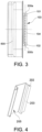
FIG. 3 is a structural schematic view of a battery matched with a terminal component in the battery apparatus according to an embodiment of the disclosure. -
FIG. 4 is a structural schematic view of a busbar in the battery apparatus according to an embodiment of the disclosure. -
FIG. 5 is a structural schematic view of a variation example of the busbar in the battery apparatus according to an embodiment of the disclosure. -
FIG. 6 is an exploded view of the busbars and insulating films in the battery apparatus according to an embodiment of the disclosure. -
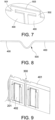
FIG. 7 is a local enlargement view of the portion B inFIG. 6 . -
FIG. 8 is a structural schematic view of a variation example of a buffer structure according to an embodiment of the disclosure. -
FIG. 9 is a structural schematic view of the busbars matched with the insulating films in the battery apparatus according to an embodiment of the disclosure. -
FIG. 10 is an exploded view of a variation example of the busbars and the insulating films in the battery apparatus according to an embodiment of the disclosure. -
FIG. 11 is a local schematic view of the structure of a variation example of the battery apparatus according to an embodiment of the disclosure. - The technical solutions in the exemplary embodiments of the disclosure will be described clearly and explicitly in conjunction with the drawings in the exemplary embodiments of the disclosure. The description proposed herein is just the exemplary embodiments for the purpose of illustrations only, not intended to limit the scope of the disclosure, so it should be understood that and various modifications and variations could be made thereto without departing from the scope of the disclosure.
- In the description of the present disclosure, unless otherwise specifically defined and limited, the terms "first", "second" and the like are only used for illustrative purposes and are not to be construed as expressing or implying a relative importance. The term "plurality" is two or more. The term "and/or" includes any and all combinations of one or more of the associated listed items.
- In particular, a reference to "the" object or "a" and "an" object is intended to denote also one of a possible plurality of such objects. Unless otherwise defined or described, the terms "connect", "fix" should be broadly interpreted, for example, the term "connect" can be "fixedly connect", "detachably connect", "integrally connect", "electrically connect" or "signal connect". The term "connect" also can be "directly connect" or "indirectly connect via a medium". For the persons skilled in the art, the specific meanings of the abovementioned terms in the present disclosure can be understood according to the specific situation.
- Further, in the description of the present disclosure, it should be understood that spatially relative terms, such as "above", "below" "inside", "outside" and the like, are described based on orientations illustrated in the figures, but are not intended to limit the exemplary embodiments of the present disclosure.
- In the context, it should also be understood that when an element or features is provided "outside" or "inside" of another element(s), it can be directly provided "outside" or "inside" of the other element, or be indirectly provided "outside" or "inside" of the another element(s) by an intermediate element.
- With reference to
FIG. 1 to FIG. 11 , the present embodiment provides a battery apparatus including aterminal component 100 and abusbar 200. At least one of theterminal component 100 and thebusbar 200 is provided with a welding identification portion, and the welding identification portion includes twonotches 300 opposite to each other. - In the battery apparatus provided by this embodiment, by arranging the welding identification portion on the
terminal component 100, by arranging the welding identification portion on thebusbar 200, or by arranging welding identification portions on both theterminal component 100 as well as thebusbar 200, the positioning accuracy of welding is improved. The welding identification portion includes twoopposite notches 300, and the twonotches 300 may define a welding region between theterminal component 100 and thebusbar 200. To be specific, the twonotches 300 may define the center of the welding region between theterminal component 100 and thebusbar 200, so that the positioning accuracy of welding between theterminal component 100 and thebusbar 200 is improved. - In an embodiment, the battery apparatus further includes a
battery 600, and theterminal component 100 is connected to thebattery 600. - In an embodiment, the
terminal component 100 includes aterminal 103 and an insulating member. Theterminal 103 includes afirst welding surface 104, at least a portion of the insulating member is located at two ends of thefirst welding surface 104, and the welding identification portion is disposed on the insulating member. Thebusbar 200 is provided with a relief space to expose the welding identification portion on the insulating member. - Exemplarily, with reference to
FIG. 3 , the welding region may be formed by thefirst welding surface 104 of theterminal 103. The contour of thefirst welding surface 104 is generally rectangular. Theterminal 103 has two opposite long sides and two opposite short sides, and the length of the long sides is greater than the length of the short sides. The two short sides are individually named as a first short side and a second short side. One of the long sides is connected to a large surface of thebattery 600, and the two short sides are both perpendicular to the large surface of thebattery 600, where the large surface of thebattery 600 refers to the side surface of the battery with the largest area. - In some embodiments, the insulating member and the
terminal 103 are injection-molded. The insulating member includes a first insulatingportion 101 and a secondinsulating portion 102. The firstinsulating portion 101 is located on the first short side, the secondinsulating portion 102 is located on the second short side, and the firstinsulating portion 101 and the secondinsulating portion 102 are opposite to each other. - The welding identification portion is arranged on the insulating member, and to be specific, the welding identification portion is provided on the first
insulating portion 101 and the secondinsulating portion 102. In order to ensure that thebusbar 200 may not block the welding identification portion during welding, afirst relief space 202 is provided on thebusbar 200 to expose the welding identification portion on the insulating member. - Exemplarily, with reference to
FIG. 1 and FIG. 2 , flanges are formed on both sides of thebusbar 200, and the flangesform welding ends 201 of thebusbar 200. The number ofwelding ends 201 is two, and the twowelding ends 201 are configured to be connected to the positive and negative electrodes of twoadjacent batteries 600. - The
first relief space 202 is a concave portion provided on the flange, and exemplarily, the concave portion is a right-angle notch. - It should be noted that the form of the relief space is not limited to the above, as long as the welding identification portion on the insulating member is exposed through the relief space.
- In an embodiment, the two
opposite notches 300 are axisymmetrically arranged. To be specific, the twoopposite notches 300 are axisymmetrically arranged with respect to the center line (the double-dotted line inFIG. 3 ) of theterminal component 100 perpendicular to the large surface of thebattery 600 as the axis of symmetry. - Exemplarily, the
notches 300 are of an axisymmetric structure, the axis of symmetry is the center line of thenotches 300, and the intersection of the axis of symmetry and the edge of thenotches 300 is the midpoint of thenotches 300. - In an embodiment, the two
opposite notches 300 are located at two ends of thefirst welding surface 104. - With reference to
FIG. 3 , the twoopposite notches 300 are individually named as afirst notch 300a and asecond notch 300b, thefirst notch 300a is disposed on the firstinsulating portion 101, and thesecond notch 300b is disposed on the secondinsulating portion 102. - In an embodiment, a connecting line between midpoints of the two
opposite notches 300 is a welding reference line. - To be specific, the connecting line between the midpoint of the
first notch 300a and the midpoint of thesecond notch 300b is the welding reference line. With reference toFIG. 3 , the dotted line represents the welding reference line. - Exemplarily, both the
first notch 300a and thesecond notch 300b are V-shaped notches. Each V-shaped notch has a tip, and the tip is the midpoint of the V-shaped notch. The tips of the two V-shaped notches are facing each other, and the connecting line between the tips of the two V-shaped notches is the welding reference line. It should be noted that the welding reference line is a virtual straight line. - When the
busbar 200 and the terminal 103 are welded by the welding equipment, the welding equipment may recognize the welding reference line. Further, the welding torch swings on both sides of the reference line, so that the accuracy of welding is ensured. - It should be noted that the welding equipment is in the related art, and its structure and working principle is not to be described herein in detail.
- In an embodiment, the welding reference line overlaps a center line of a welding surface of the
terminal component 100. - With reference to
FIG. 3 , the dashed-dotted line represents the center line of thefirst welding surface 104 of theterminal component 100, and in order to ensure the clarity of the illustration, the dashed line inFIG. 3 is thickened. The dotted line overlaps the dashed line. When the welding trajectory of the welding torch oscillates on both sides of the welding reference line, it is ensured that the welding trajectory is located on both sides of the center line of thefirst welding surface 104. In this way, thebusbar 200 is prevented from being welded onto the insulating member of theterminal component 100. - In an embodiment, the
busbar 200 has asecond welding surface 203, and a contour of thesecond welding surface 203 overlaps a contour of thefirst welding surface 104. - The
busbar 200 has afirst surface 204 and asecond surface 205 opposite to each other. To be specific, each weldingend 201 of thebusbar 200 has a surface facing away from the battery and a surface facing the battery. Herein, the surface of thewelding end 201 facing away from the battery is a portion of thefirst surface 204 of thebusbar 200, and the surface of thewelding end 201 facing the battery is a portion of thesecond surface 205 of thebusbar 200. - The
second welding surface 203 is the surface of thewelding end 201 of thebusbar 200 facing the battery. That is, thesecond welding surface 203 is adhered to thefirst welding surface 104 and is fixed by welding. The contour of thesecond welding surface 203 substantially overlaps the contour of thefirst welding surface 104, an in this way, it is ensured that thesecond welding surface 203 is aligned with thefirst welding surface 104, and precise welding may thus be easily performed. - It should be noted that, the contour of the
second welding surface 203 overlapping the contour of thefirst welding surface 104 means that the contour of thesecond welding surface 203 and the contour of thefirst welding surface 104 substantially overlap. - In an embodiment, the first relief space is formed by the welding identification portion disposed on the
busbar 200. That is, both the insulating member of theterminal component 100 and thebusbar 200 are provided with welding identification portions. - Exemplarily, the welding identification portion on the
busbar 200 overlaps the welding identification portion on the insulating member. To be specific, the welding identification portion on thebusbar 200 also includes two V-shaped notches. The two V-shaped notches are opposite to each other and are arranged at both ends of the flanges, and the V-shaped notches on the flanges correspond to the V-shaped notches on the insulating member one by one. - It should be noted that the welding identification portion on the
busbar 200 and the welding identification portion on the insulating member may also partially overlap. Exemplarily, the projections of the tips of the V-shaped notches on the flanges overlap the tips of the V-shaped notches on the insulating member corresponding to their positions on the first welding surface, or the projections of the tips of the V-shaped notches on the flanges on the first welding surface is located outside the V-shaped notches on the insulating member. The included angle between the two side walls of each V-shaped notch on the flange is not less than the included angle between the two side walls of each V-shaped notch on the insulating member. - In some embodiments, the welding identification portion may also be arranged only on the
busbar 200. With reference toFIG. 5 , the welding identification portion on thebusbar 200 also includes twonotches 300, and the twonotches 300 are opposite to each other and are arranged at both ends of the flange. Both the notches are V-shaped notches. - It should be noted that the shape of the two
notches 300 is not limited to be V-shaped, as long as the connecting line between the twonotches 300 may be easily recognized by the welding equipment. For instance, the shape of the twonotches 300 may also be U-shaped, trapezoidal, or rectangular. - In an embodiment, a plurality of
busbars 200 are provided, and insulatingfilms 400 are provided on outer surfaces of the plurality ofbusbars 200. Each of the insulatingfilms 400 is provided with a second relief space, and the second relief space corresponds to the welding region to expose the welding region. The insulatingfilms 400 on twoadjacent busbars 200 are connected through abuffer structure 500. - In order to facilitate welding and further improve the welding efficiency, an insulating
film 400 is provided on the outer surface of eachbusbar 200, and the insulatingfilms 400 on twoadjacent busbars 200 are connected as a whole through thebuffer structure 500 to form a wire harness assembly. - Exemplarily, with reference to
FIG. 6 , the second relief space may be arelief hole 403, and therelief hole 403 corresponds to the welding ends 201, so that the welding region on the welding ends 201 is exposed, and the welding ends 201 may be easily welded and fixed onto theterminal 103 of the battery. - It should be noted that each second relief space is not limited to the
relief hole 403, but may also be an open second relief space. For instance, the insulatingfilm 400 includes two sub-film segments, a gap is provided between the two sub-film segments in the length direction of thebusbar 200, and the space between the two sub-film segments is the second relief space. As long as it can be ensured that the welding region on the welding ends 201 of thebusbar 200 is exposed to the outside of the insulatingfilm 400. - Since the
buffer structure 500 may improve the buffer strength between thebusbars 200, tearing of the insulatingfilms 400 caused by the stress concentration between thebusbars 200 may be prevented from occurring as much as possible during assembly or use. - In some embodiments, the insulating
films 400 are bonded and fixed to thebusbars 200, so that the fixing strength of thebusbars 200 may be ensured, and the deviation of thebusbars 200 from the welding positions is prevented from occurring. - In an embodiment, the
buffer structure 500 and the insulatingfilm 400 are integrally formed. To be specific, thebuffer structure 500 is a portion of the insulatingfilm 400. In this way, the overall mechanical strength and buffering performance of the insulatingfilm 400 are improved, the tearing of the insulatingfilm 400 caused by the stress concentration between thebusbars 200 is prevented from occurring, and the service life of the wire harness assembly is prolonged. - The
buffer structure 500 and the insulatingfilm 400 are integrally formed, and thebusbars 200 may thus be integrated to form a wire harness assembly, which is convenient for assembly. - In an embodiment, each
buffer structure 500 includes an elastic member, gaps are provided between at least portions of thebuffer structure 500 and the insulatingfilms 400, or thebuffer structure 500 is a curved structure located between twoadjacent busbars 200. - In some embodiments, the
buffer structures 500 includes the elastic members. Exemplarily, thebuffer structures 500 are elastic films. Eachbuffer structure 500 may be connected between two adjacent insulatingfilms 400 or may be connected across the top ends or bottom ends of the two adjacent insulatingfilms 400. Alternatively, onebuffer structure 500 is connected across the top ends of two adjacent insulatingfilms 400, and onebuffer structure 500 is also connected across the bottom ends of the two adjacent insulatingfilms 400. When thebuffer structure 500 is connected across the top or bottom ends of two adjacent insulatingfilms 400, a gap is provided between the two adjacent insulatingfilms 400, and thebuffer structure 500 is connected to the two adjacent insulatingfilms 400 across the gap, so as to ensure that thebuffer structure 500 may be elastically deformed. - In an embodiment, with reference to
FIG. 8 , thebuffer structure 500 is a curved structure located between two adjacent insulatingfilms 400. - The two adjacent insulating
films 400 are integrally formed with the curved structure, that is, the curved structure is a portion of the insulatingfilms 400. After thebusbar 200 is welded and fixed to theterminal 103 of the battery, the curved structure is located between twoadjacent busbars 200. - Exemplarily, since two
notches 300 are arranged opposite to each other at two ends of thefirst welding surface 104 of the terminal 103, the connecting line between the twoopposite notches 300 is a welding reference line. When thebusbar 200 is welded onto theterminal 103 of the battery, the welding equipment may recognize the abovementioned welding reference line and oscillate on both sides of the welding reference line, and precise welding is thus achieved. After the welding is completed, the curved structure is located between twoadjacent busbars 200, so that the stress concentration between thebusbars 200 may be relieved or eliminated during subsequent use (e.g., when the battery swells), and the risk of tearing of the insulatingfilms 400 is effectively reduced. - In some embodiments, gaps are provided between at least portions of the
buffer structure 500 and the insulatingfilms 400. - To be specific, a gap is provided between two adjacent insulating
films 400, that is, a gap is provided between two sidewalls of two adjacent insulatingfilms 400 that are close to each other. Gaps being provided between at least portions of thebuffer structure 500 and the insulatingfilms 400 ensures that a buffer space is provided between the first film segment and the second film segment. - Gaps may be provided between at least portions of the
buffer structure 500 and the top ends of the insulatingfilms 400 or the sidewalls of the insulatingfilms 400. Herein, with reference toFIG. 6 andFIG. 11 , the top and bottom ends of the insulatingfilms 400 refer to the edges of the insulatingfilms 400 parallel to the arrow direction X, and the sidewalls of the insulatingfilms 400 refer to the sides of the insulatingfilms 400 that are perpendicular to the top and bottom ends thereof. - Exemplarily, each the
buffer structure 500 includes afirst connection segment 501, asecond connection segment 502, and athird connection segment 503. Thefirst connection segment 501 is connected to one of the insulatingfilms 400, thesecond connection segment 502 is connected to another insulatingfilm 400, and thethird connection segment 503 is connected between thefirst connection segment 501 and thesecond connection segment 502, so that thebuffer structure 500 is formed into a zigzag structure. - Exemplarily, the number of
buffer structures 500 is two, and the twobuffer structures 500 are formed integrally with the insulatingfilms 400. One of thebuffer structures 500 is connected above two adjacent insulatingfilms 400, and theother buffer structure 500 is connected below two adjacent insulatingfilms 400. - The following description will be given by taking the
buffer structure 500 connected above two adjacent insulatingfilms 400 as an example. - To be specific, with reference to
FIG. 7 , thefirst connection segment 501 is integrally formed with the top end of one of the insulatingfilms 400, thesecond connection segment 502 is integrally formed with the top end of another insulatingfilm 400, and thethird connection segment 503 is connected between thefirst connection segment 501 and thesecond connection segment 502, so that thebuffer structure 500 is formed into a zigzag structure. Herein, gaps are provided between thethird connection segment 503 and the top ends of two adjacent insulatingfilms 400, and a gap is also provided between the two adjacent insulatingfilms 400. When twoadjacent busbars 200 tend to move away from each other, at least thefirst connection segment 501 and thesecond connection segment 502 are deformed in the stacking direction of the batteries, and a buffering effect is thus provided. In this way, the tearing of the insulatingfilms 400 caused by the stress concentration between thebusbars 200 is prevented from occurring, and the service life of the wire harness assembly is prolonged. - In an embodiment, the
first connection segment 501, thesecond connection segment 502, and thethird connection segment 503 are integrally formed. To be specific, thefirst connection segment 501, thesecond connection segment 502, and thethird connection segment 503 are integrally formed with the insulatingfilms 400. In this way, production and processing may be easily performed, and the overall structural strength and buffering performance of the wire harness assembly may be improved. - It should be noted that the
buffer structure 500 may also be an S-shaped structure or a Z-shaped structure. The S-shaped structure and the Z-shaped structure may be connected in a gap between two adjacent insulatingfilms 400. - It should be noted that the
buffer structure 500 is not limited to the above several forms, and other forms of thebuffer structure 500 may also be selected according to actual needs. - In some embodiments, each insulating
film 400 includes a firstinsulating film 401 and a secondinsulating film 402, the first insulating film is located on thefirst surface 204 of thebusbar 200, and the secondinsulating film 402 is located on thesecond surface 205 of thebusbar 200. - With reference to
FIG. 4 ,FIG. 9 , andFIG. 10 , the first insulatingfilm 401 is adhered to at least a portion of thefirst surface 204 of thebusbar 200, and the secondinsulating film 402 is adhered to at least a portion of thesecond surface 205 of thebusbar 200. In this way, the fixing strength of the insulatingfilm 400 to thebusbar 200 may be enhanced, and the problem of inaccurate welding and positioning caused by the loosening of thebusbar 200 may be prevented from occurring. - The second relief space includes a first through
hole 4011 arranged on the first insulatingfilm 401 and a second throughhole 4021 arranged on the secondinsulating film 402. To be specific, the first throughhole 4011 on the first insulatingfilm 401 may expose at least a portion of the surface of thewelding end 201 facing away from the battery, and the second throughhole 4021 on the secondinsulating film 402 may expose at least a portion of the surface of thewelding end 201 facing the battery. In this way, it is convenient to use welding equipment to weld and fix thewelding end 201 on theterminal 103 of the battery. That is, it is convenient to use welding to weld the welding region between theterminal component 100 and thebusbar 200. - It should be understood that the first through
hole 4011 and the second throughhole 4021 together form the second relief space. - In some embodiments, with reference to
FIG. 10 , the number ofbuffer structures 500 is two, and the twobuffer structures 500 are formed integrally with the first insulatingfilm 401. - In an embodiment, first insulating
film 401 is connected to the secondinsulating film 402 through hot pressing. - The first
insulating film 401 and the secondinsulating film 402 are connected by a hot pressing process, so that thebusbar 200 is fixed between the first insulatingfilm 401 and the secondinsulating film 402. Herein, the hot pressing process is the related art, and description thereof is not provided in detail herein. - It should be noted that the first insulating
film 401 and the secondinsulating film 402 may also be integrally formed, as long as thebusbar 200 may be fixed and thewelding end 201 of thebusbar 200 may be welded and fixed to theterminal 103 of the battery. - Other embodiments of the disclosure will be apparent to those skilled in the art from consideration of the specification and practice of the disclosure disclosed herein. The disclosure is intended to cover any variations, uses or adaptations of the disclosure. These variations, uses, or adaptations follow the general principles of the disclosure and include common general knowledge or conventional technical means in the art that are not disclosed in the present disclosure.
Claims (11)
- A battery apparatus, comprising a terminal component (100) and a busbar (200), wherein at least one of the terminal component (100) and the busbar (200) is provided with a welding identification portion, and the welding identification portion comprises two notches (300) opposite to each other.
- The battery apparatus according to claim 1, wherein the two opposite notches (300) are axisymmetrically arranged.
- The battery apparatus according to claim 1, wherein the terminal component (100) comprises a terminal (103) and an insulating member, the terminal (103) comprises a first welding surface (104), at least a portion of the insulating member is located at two ends of the first welding surface (104), the welding identification portion is disposed on the insulating member, and the busbar (200) is provided with a first relief space (202) to expose the welding identification portion on the insulating member.
- The battery apparatus according to claim 3, wherein the two opposite notches (300) are located at two ends of the first welding surface (104).
- The battery apparatus according to claim 3, wherein the busbar (200) has a second welding surface (203), and a contour of the second welding surface (203) overlaps a contour of the first welding surface (104).
- The battery apparatus according to claim 3, wherein the first relief space (202) is formed by the welding identification portion disposed on the busbar (200).
- The battery apparatus according to claim 1, wherein a connecting line between midpoints of the two opposite notches (300) is a welding reference line.
- The battery apparatus according to claim 7, wherein the welding reference line overlaps a center line of a welding surface of the terminal component (100).
- The battery apparatus according to any one of claims 1-8, wherein both the two notches (300) are V-shaped notches.
- The battery apparatus according to any one of claims 1-8, wherein a plurality of busbars (200) are provided, insulating films (400) are provided on outer surfaces of the plurality of busbars (200), each of the insulating films (400) is provided with a second relief space, the second relief space corresponds to welding ends of the busbar (200) to expose at least portions of the welding ends, and the insulating films on two adjacent busbars (200) are connected through a buffer structure (500).
- The battery apparatus according to claim 10, wherein each buffer structure (500) comprises an elastic member, gaps are provided between at least portions of the buffer structure (500) and the insulating films (400), or the buffer structure (500) is a curved structure located between two adjacent busbars (200).
Applications Claiming Priority (1)
| Application Number | Priority Date | Filing Date | Title |
|---|---|---|---|
| CN202210534851.9A CN114914636A (en) | 2022-05-17 | 2022-05-17 | Battery pack |
Publications (2)
| Publication Number | Publication Date |
|---|---|
| EP4290671A2 true EP4290671A2 (en) | 2023-12-13 |
| EP4290671A3 EP4290671A3 (en) | 2024-06-12 |
Family
ID=82768656
Family Applications (1)
| Application Number | Title | Priority Date | Filing Date |
|---|---|---|---|
| EP22202379.8A Pending EP4290671A3 (en) | 2022-05-17 | 2022-10-19 | Battery apparatus |
Country Status (3)
| Country | Link |
|---|---|
| US (1) | US12469933B2 (en) |
| EP (1) | EP4290671A3 (en) |
| CN (1) | CN114914636A (en) |
Families Citing this family (1)
| Publication number | Priority date | Publication date | Assignee | Title |
|---|---|---|---|---|
| CN116053672A (en) * | 2023-01-13 | 2023-05-02 | 中创新航科技股份有限公司 | Battery, manufacturing method thereof, and battery device |
Family Cites Families (7)
| Publication number | Priority date | Publication date | Assignee | Title |
|---|---|---|---|---|
| US10199626B2 (en) * | 2017-04-28 | 2019-02-05 | Nio Usa, Inc. | Spring loaded busbar for laser welding operation |
| CN206820036U (en) * | 2017-05-19 | 2017-12-29 | 福州华鹰重工机械有限公司 | A kind of outer cover unit of battery pack, modular unit and battery bag |
| CN110911594B (en) | 2018-09-14 | 2024-09-06 | 宁德时代新能源科技股份有限公司 | Battery module and its busbar component and busbar assembly |
| WO2020235279A1 (en) | 2019-05-22 | 2020-11-26 | 三洋電機株式会社 | Bus bar plate |
| CN210744017U (en) * | 2019-10-21 | 2020-06-12 | 宁德时代新能源科技股份有限公司 | Wire harness isolation board assembly, battery module, battery pack and device |
| CN216413212U (en) | 2021-12-01 | 2022-04-29 | 宁德时代新能源科技股份有限公司 | Busbar assembly, battery and power consumption device |
| CN217306697U (en) * | 2022-05-17 | 2022-08-26 | 中创新航科技股份有限公司 | Battery pack |
-
2022
- 2022-05-17 CN CN202210534851.9A patent/CN114914636A/en active Pending
- 2022-10-18 US US17/967,900 patent/US12469933B2/en active Active
- 2022-10-19 EP EP22202379.8A patent/EP4290671A3/en active Pending
Also Published As
| Publication number | Publication date |
|---|---|
| CN114914636A (en) | 2022-08-16 |
| US20230378617A1 (en) | 2023-11-23 |
| EP4290671A3 (en) | 2024-06-12 |
| US12469933B2 (en) | 2025-11-11 |
Similar Documents
| Publication | Publication Date | Title |
|---|---|---|
| EP2528143B1 (en) | Power storage element provided with a current collector, and method of manufacturing current collector | |
| KR101818631B1 (en) | Battery and method of manufacturing same | |
| KR101887242B1 (en) | Electric storage device and spacer | |
| JP2016129125A (en) | Power storage device | |
| EP4290671A2 (en) | Battery apparatus | |
| CN117766955A (en) | Secondary battery | |
| CN217306697U (en) | Battery pack | |
| KR20230012419A (en) | Terminal component and method for manufacturing the same | |
| JP4146665B2 (en) | Sealed secondary battery | |
| US20250226542A1 (en) | Battery pack | |
| EP4030537B1 (en) | Secondary battery and manufacturing method therefor, battery module, and apparatus | |
| CN108292732A (en) | Battery | |
| EP3598530A1 (en) | Connection member for connecting to a busbar of a battery, battery | |
| CN217306688U (en) | Wire harness assembly and battery pack | |
| JPH06215754A (en) | Battery pack | |
| CN220574982U (en) | Ultrasonic welding equipment | |
| JPH09213298A (en) | Storage batteries and electrode plates for storage batteries | |
| US20230019424A1 (en) | Horn, terminal component, and secondary battery | |
| EP4492561A1 (en) | Battery, and method for manufacturing battery | |
| JPH11176413A (en) | Battery current collector | |
| JPH11167912A (en) | Battery pack | |
| JP2003346903A (en) | Battery | |
| JP2018152224A (en) | Battery pack | |
| CN212810293U (en) | Jumper wire structure for bridge rectifier and rectifier | |
| EP3531478A1 (en) | Current blocking structure applied to pouch type secondary battery |
Legal Events
| Date | Code | Title | Description |
|---|---|---|---|
| PUAI | Public reference made under article 153(3) epc to a published international application that has entered the european phase |
Free format text: ORIGINAL CODE: 0009012 |
|
| STAA | Information on the status of an ep patent application or granted ep patent |
Free format text: STATUS: REQUEST FOR EXAMINATION WAS MADE |
|
| 17P | Request for examination filed |
Effective date: 20221019 |
|
| AK | Designated contracting states |
Kind code of ref document: A2 Designated state(s): AL AT BE BG CH CY CZ DE DK EE ES FI FR GB GR HR HU IE IS IT LI LT LU LV MC ME MK MT NL NO PL PT RO RS SE SI SK SM TR |
|
| PUAL | Search report despatched |
Free format text: ORIGINAL CODE: 0009013 |
|
| AK | Designated contracting states |
Kind code of ref document: A3 Designated state(s): AL AT BE BG CH CY CZ DE DK EE ES FI FR GB GR HR HU IE IS IT LI LT LU LV MC ME MK MT NL NO PL PT RO RS SE SI SK SM TR |
|
| RIC1 | Information provided on ipc code assigned before grant |
Ipc: H01M 50/502 20210101AFI20240506BHEP |